EP2897121B1 - Interferenzunterdrückungsvorrichtung und -verfahren - Google Patents
Interferenzunterdrückungsvorrichtung und -verfahren Download PDFInfo
- Publication number
- EP2897121B1 EP2897121B1 EP13883347.0A EP13883347A EP2897121B1 EP 2897121 B1 EP2897121 B1 EP 2897121B1 EP 13883347 A EP13883347 A EP 13883347A EP 2897121 B1 EP2897121 B1 EP 2897121B1
- Authority
- EP
- European Patent Office
- Prior art keywords
- interference prevention
- interference
- connection wire
- module
- prevention material
- Prior art date
- Legal status (The legal status is an assumption and is not a legal conclusion. Google has not performed a legal analysis and makes no representation as to the accuracy of the status listed.)
- Active
Links
Images


Classifications
-
- H—ELECTRICITY
- H01—ELECTRIC ELEMENTS
- H01B—CABLES; CONDUCTORS; INSULATORS; SELECTION OF MATERIALS FOR THEIR CONDUCTIVE, INSULATING OR DIELECTRIC PROPERTIES
- H01B11/00—Communication cables or conductors
- H01B11/18—Coaxial cables; Analogous cables having more than one inner conductor within a common outer conductor
-
- H—ELECTRICITY
- H05—ELECTRIC TECHNIQUES NOT OTHERWISE PROVIDED FOR
- H05K—PRINTED CIRCUITS; CASINGS OR CONSTRUCTIONAL DETAILS OF ELECTRIC APPARATUS; MANUFACTURE OF ASSEMBLAGES OF ELECTRICAL COMPONENTS
- H05K9/00—Screening of apparatus or components against electric or magnetic fields
- H05K9/0073—Shielding materials
- H05K9/0098—Shielding materials for shielding electrical cables
-
- H—ELECTRICITY
- H05—ELECTRIC TECHNIQUES NOT OTHERWISE PROVIDED FOR
- H05K—PRINTED CIRCUITS; CASINGS OR CONSTRUCTIONAL DETAILS OF ELECTRIC APPARATUS; MANUFACTURE OF ASSEMBLAGES OF ELECTRICAL COMPONENTS
- H05K9/00—Screening of apparatus or components against electric or magnetic fields
- H05K9/0064—Earth or grounding circuit
Definitions
- the present invention relates to the field of electronic technologies, and in particular, to an interference prevention apparatus and method.
- US 2011/0266050 A1 relates to a cable bundling structure.
- the structure comprises a cable with a plurality of conductor units extending in an extension direction and arranged together to form a bundled arrangement.
- the bundled arrangement forms a wrapped section.
- the structure comprises at least one helical wrap member which wraps around the wrapped section of the target cable to bundle the conductor units of the wrapped section together to form the bundled arrangement.
- the structure comprises the helical wrap member having at least one section of wrapping turns, which is made in a one-piece form having a predetermined wrap width, a predetermined helix angle, and a predetermined wrap diameter and extending a predetermined length in a wrapping direction.
- the helical wrap member helically wraps around the target cable in such a way that the helical wrap member is set in slidable engagement with the target cable and serves as an external protection for the cable.
- MARMOR S "circulation des depends dans les masses mais", TOUTE L-ELECTRONIQUE, no. 376, 1 April 1973 (1973-04-01), pages 89-93, XP001452612 examines the application of grounding coax cables, assembly of chassis on a common metal plate and functionality of hardened frames.
- Embodiments of the present invention are defined by the claims.
- An interference prevention apparatus and method are provided, which can effectively reduce electromagnetic radiation interference generated in a circuit at a low cost.
- an interference prevention apparatus including an interference prevention module and a control module, where
- the interference prevention apparatus further includes a connector connecting the interference prevention module and the control module, where
- the interference prevention material is an interference blocking material
- the at least one first connection wire is wrapped by the interference prevention material
- a length of the interference prevention material is less than a length of the at least one first connection wire.
- the interference blocking material includes at least one of the following materials: copper foil, aluminum foil, silver foil, a conductive fabric, or a shielding coating.
- the interference prevention material is adhered to a set position of the at least one first connection wire.
- the interference prevention material is an electrically conductive double-sided adhesive tape.
- an interference prevention method including:
- the receiving a working signal sent by a control apparatus is specifically:
- the interference prevention material is an interference blocking material
- the at least one first connection wire is wrapped by the interference prevention material
- a length of the interference prevention material is less than a length of the at least one first connection wire.
- the interference blocking material includes at least one of the following materials: copper foil, aluminum foil, silver foil, a conductive fabric, or a shielding coating.
- the interference prevention material is adhered to a set position of the at least one first connection wire.
- the interference prevention material is an electrically conductive double-sided adhesive tape.
- a connection wire between a control module and an interference prevention module is divided by using an interference prevention material, which reduces a loop area of a return current signal and can effectively reduce electromagnetic radiation interference generated in a circuit at a low cost.
- FIG. 1 is a schematic diagram of electromagnetic radiation interference generated in a circuit.
- a control module 1 is connected to a first component 3 by using a connector 2, and the control module 1 provides a control signal and a data signal for the first component 3, so as to control the first component to work.
- the first component 3 may be an LCD, and the control module 1 controls the LCD to perform display.
- electromagnetic interference radiation 6 generated by a return current signal 5 between the first component 3 and the connector 2 is great.
- electromagnetic radiation includes differential-mode radiation and common-mode radiation.
- the differential-mode radiation is analyzed by using a current loop model, and calculation formulas of radiated electromagnetic fields in a near field region and a far field region are as follows:
- I 1 and h are loop currents; A 1 and A 2 are loop areas; D 1 and D 2 are distances from observation points to loops; Zo 1 and Zo 2 are impedance in free space; ⁇ 1 and ⁇ 2 are wavelengths corresponding to current frequencies; H 1 and E 1 are respectively a magnetic field strength and an electric field strength of the near field region of the differential-mode radiation; and H 2 and E 2 are respectively electric field strengths of the near field region and the far field region of the differential-mode radiation.
- I 3 and I 4 are loop currents; L 3 and L 4 are lengths of conducting wires; D 3 and D 4 are distances from observation points to loops; Zo 3 and Zo 4 are impedance in free space; ⁇ 3 and ⁇ 4 are wavelengths corresponding to current frequencies; H 3 and E 3 are respectively a magnetic field strength and an electric field strength of the near field region of the common-mode radiation; H 4 and E 4 are respectively a magnetic field strength and an electric field strength of the far field region of the common-mode radiation.
- the differential-mode radiation of the near field region and the far field region may be reduced by reducing a loop current, a wavelength, or a loop area; and the common-mode radiation of the near field region and the far field region may also be reduced by reducing a loop current, a wavelength, or a length of a conducting wire.
- the two methods of reducing a loop current and a wavelength there are limitations on the two methods of reducing a loop current and a wavelength.
- FIG. 2 is a structural diagram of an interference prevention apparatus according to an embodiment of the present invention.
- an interference prevention apparatus 20 includes: a control module 1 and an interference prevention module 9.
- the control module 1 is configured to send a working signal to the interference prevention module 9, where the working signal may be a control signal or a data signal or both.
- the interference prevention module 9 is configured to receive the working signal, and control a working state of a first component 3 in the interference prevention module 9 according to the working signal, and the first component 3 and the control module 1 may be connected by using one or more connection wires 4.
- the interference prevention module 9 is further configured to send a return current signal to the control module 1.
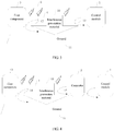
- FIG. 3 is a schematic diagram of a principle of performing electromagnetic interference radiation prevention by an interference prevention apparatus according to an embodiment of the present invention.
- a control module 1 sends a control signal or a data signal or both to an interference prevention module 9; the interference prevention module 9 receives the control signal or the data signal or both, and controls a working state of a first component 3. For example, according to the control signal, the interference prevention module 9 controls enabling or disabling of the first component 3, and controls output of the data signal on the first component 3, and so on.
- the interference prevention module 9 includes the first component 3, a connection wire 4, and an interference prevention material 10, the connection wire 4 is divided into at least two segments by using the interference prevention material 10, and the interference prevention material 10 is connected to ground 11.
- a return current signal is shunted to two current return loops 12 and 13, and a return current signal in the current return loop 12 flows to the control module 1 through the interference prevention material 10 and the ground 11, and a return current signal in the current return loop 13 flows to the control module 1 through the ground 11.
- areas of the current return loops 12 and 13 in this embodiment are separately reduced, and according to the foregoing formulas, electromagnetic radiation interference generated by the return current signal is reduced.
- FIG. 4 is a schematic diagram of a principle of performing electromagnetic interference radiation prevention by an interference prevention apparatus according to another embodiment of the present invention. As shown in FIG. 4 , differences from FIG. 3 lie in that: a first component 3 in the interference prevention apparatus is connected to a control module 1 by using a connector 2, and the control module 1 sends a control signal or data signal or both to the first component 3 by using the connector 2; a connection wire 4 between the first component 3 and the connector 2 is divided into at least two segments by an interference prevention material 10, and the interference prevention material 10 is connected to ground 11; and a return current signal is shunted to at least two current return loops 14 and 15, and a return current signal in the current return loop 14 flows to the control module 1 through the interference prevention material 10 and the ground 11, and a return current signal in the current return loop 15 flows to the control module 1 through the ground 11.
- the interference prevention material may be an interference blocking material
- the interference blocking material includes: any one of copper foil, aluminum foil, silver foil, a conductive fabric, and a shielding coating.
- FIG. 5 which is a schematic diagram of performing interference prevention processing on an interference prevention apparatus, one small segment or multiple small segments of all connection wires 4 are wrapped by an interference blocking material 10, where a length of the interference blocking material is less than a length of the connection wires 4, and a first component 3 is inserted into the connector 2 shown in FIG. 4 by using a connection wire edge connector 16.
- the interference blocking material 10 is grounded.
- a connection wire is wrapped and divided by using an interference blocking material, which not only reduces an area of a current return loop so as to reduce electromagnetic radiation interference generated by a return current signal; in addition, the interference blocking material may also play a role of further reducing the electromagnetic radiation interference; and the interference blocking material only needs to wrap one small segment or multiple small segments of the connection wire, so interference prevention costs are low.
- the interference prevention material may be an electrically conductive double-sided adhesive tape.
- one side of the electrically conductive double-sided adhesive tape is adhered to a set position of all connection wires 4 that are bound together, and the other side is adhered to the ground 11, thereby dividing the connection wires 4, and the signal of the current return loop 12 or 14 flows to the control module 1 through the electrically conductive double-sided adhesive tape and the ground.
- Using the electrically conductive double-sided adhesive tape to prevent interference can effectively reduce the electromagnetic radiation interference, and in addition, operations are simple, and interference prevention costs are low.
- ground in the embodiment of the present invention should not be understood as limited to board ground, structural ground, or the like, but should be ground in a broad sense.
- a grounding manner is not limited to the implementation manner mentioned in this embodiment either.
- a connection wire between a control module and an interference prevention module is divided by using an interference prevention material, which reduces a loop area of a return current signal, and can effectively reduce electromagnetic radiation interference generated in a circuit at a low cost.
- FIG. 6 is a method flowchart of an interference prevention method according to an embodiment of the present invention. The method includes the following steps:
- connection wires In electrical and electronic devices, generally, there are one or multiple control apparatuses that control working of each component, and these components are connected to the control apparatus by using connection wires. Because the control apparatus is generally relatively far away from these components, there is larger external interference radiation space on the connection wires, and a return current signal searches for a path with lower impedance by itself to return to a source, that is, the control apparatus, which causes failure in controlling a current return path and causes a larger area of a current return loop. Therefore, electromagnetic interference radiation generated by return current signals between these components and the control apparatus is great.
- the working signal sent by the control apparatus is received, and the working signal may be a control signal or a data signal or both.
- Step S102 Control a working state of a first component according to the working signal, where the first component is connected to the control apparatus by using at least one first connection wire, and the at least one first connection wire is divided into at least two segments by an interference prevention material, and the interference prevention material is connected to ground.
- a working state of a working component is controlled according to the received working signal. For example, according to the control signal, enabling or disabling of the first component is controlled, and output of the data signal on the first component is controlled.
- the working component and the control apparatus are connected by using one or more connection wires, the connection wire is divided into at least two segments by using the interference prevention material; the interference prevention material is connected to the ground.
- Step S103 Send a return current signal to the control apparatus, where the return current signal flows to the control apparatus through the interference prevention material.
- the return current signal is sent to the control apparatus, and the return current signal is shunted to at least two current return loops by the interference prevention material, and a return current signal in a current return loop flows to the control apparatus through the interference prevention material and the ground.
- step S101 is specifically as follows:
- the interference prevention material may be an interference blocking material
- the interference blocking material includes: any one of copper foil, aluminum foil, silver foil, a conductive fabric, or a shielding coating.
- FIG. 5 which is a schematic diagram of performing interference prevention processing on an interference prevention apparatus, one small segment or multiple small segments of all connection wires 4 are wrapped by an interference blocking material 10, where a length of the interference blocking material is less than a length of the connection wires 4, and a first component 3 is inserted into the connector 2 shown in FIG. 4 by using a connection wire edge connector 16.
- the interference blocking material 10 is grounded.
- a connection wire is wrapped and divided by using an interference blocking material, which not only reduces an area of a current return loop so as to reduce electromagnetic radiation interference generated by a return current signal; in addition, the interference blocking material may also play a role of further reducing the electromagnetic radiation interference; and the interference blocking material only needs to wrap one small segment or multiple small segments of the connection wire, so interference prevention costs are low.
- the interference prevention material may be an electrically conductive double-sided adhesive tape.
- one side of the electrically conductive double-sided adhesive tape is adhered to a set position of all connection wires 4 that are bound together, and the other side is adhered to the ground 11, thereby dividing the connection wires 4, and the signal of the current return loop 12 or 14 flows to the control module 1 through the electrically conductive double-sided adhesive tape and the ground.
- Using the electrically conductive double-sided adhesive tape to prevent interference can effectively reduce the electromagnetic radiation interference, and in addition, operations are simple, and interference prevention costs are low.
- ground in the embodiment of the present invention should not be understood as limited to board ground, structural ground, or the like, but should be ground in a broad sense.
- a grounding manner is not limited to the implementation manner mentioned in this embodiment either.
- a connection wire between a control module and an interference prevention module is divided by using an interference prevention material, which reduces a loop area of a return current signal, and can effectively reduce electromagnetic radiation interference generated in a circuit at a low cost.
Landscapes
- Engineering & Computer Science (AREA)
- Microelectronics & Electronic Packaging (AREA)
- Shielding Devices Or Components To Electric Or Magnetic Fields (AREA)
- Devices For Indicating Variable Information By Combining Individual Elements (AREA)
- Cable Transmission Systems, Equalization Of Radio And Reduction Of Echo (AREA)
- Patch Boards (AREA)
Claims (6)
- Störungsverhinderungsvorrichtung (20), die ein Störungsverhinderungsmodul (9) und ein Steuermodul (1) umfasst, wobei
das Steuermodul (1) ausgelegt ist zum Senden eines Arbeitssignals zu dem Störungsverhinderungsmodul (9);
das Störungsverhinderungsmodul (9) ausgelegt ist zum Empfangen des Arbeitssignals und Steuern eines Arbeitszustands einer ersten Komponente (3) gemäß dem Arbeitssignal, wobei die erste Komponente (3) durch Verwendung mindestens einer ersten Verbindungsleitung (4) mit dem Steuermodul (1) verbunden ist, die mindestens eine erste Verbindungsleitung (4) durch ein Störungsverhinderungsmaterial (10) in mindestens zwei Segmente aufgeteilt ist und
das Störungsverhinderungsmaterial (10) mit Masse (11) verbunden ist; und
das Störungsverhinderungsmodul (9) ferner ausgelegt ist zum Senden eines Rückstromsignals zu dem Steuermodul (1), wobei das Rückstromsignal durch das Störungsverhinderungsmaterial (10) zu dem Steuermodul (1) fließt, wobei das Störungsverhinderungsmaterial an eine festgesetzte Position der mindestens einen ersten Verbindungsleitung geklebt ist und das Störungsverhinderungsmaterial ein elektrisch leitfähiges doppelseitiges Klebeband ist. - Störungsverhinderungsvorrichtung (20) nach Anspruch 1, die ferner einen Verbinder (2) umfasst, der das Störungsverhinderungsmodul (9) und das Steuermodul (1) verbindet, wobei
der Verbinder (2) ausgelegt ist zum Empfangen des Arbeitssignals und Senden des Arbeitssignals zu dem Störungsverhinderungsmodul (9). - Störungsverhinderungsvorrichtung (20) nach Anspruch 1 oder 2, wobei das Störungsverhinderungsmaterial (10) ein Störungsblockierungsmaterial ist, die mindestens eine erste Verbindungsleitung (4) von dem Störungsverhinderungsmaterial (10) umwickelt ist und eine Länge des Störungsverhinderungsmaterials (10) geringer als eine Länge der mindestens einen ersten Verbindungsleitung (4) ist.
- Störungsverhinderungsverfahren, umfassend:Empfangen (S101) eines durch eine Steuervorrichtung (1) gesendeten Arbeitssignals;Steuern (S102) eines Arbeitszustands einer ersten Komponente (3) gemäß dem Arbeitssignal, wobei die erste Komponente (3) durch Verwendung mindestens einer ersten Verbindungsleitung (4) mit der Steuervorrichtung (1) verbunden ist, die mindestens eine erste Verbindungsleitung (4) durch ein Störungsverhinderungsmaterial (10) in mindestens zwei Segmente aufgeteilt wird und das Störungsverhinderungsmaterial (10) mit Masse (11) verbunden ist; undSenden (S103) eines Rückstromsignals zu der Steuervorrichtung (1), wobei das Rückstromsignal durch das Störungsverhinderungsmaterial (10) zu der Steuervorrichtung (1) fließt, wobeidas Störungsverhinderungsmaterial an eine festgesetzte Position der mindestens einen ersten Verbindungsleitung (4) geklebt wird und das Störungsverhinderungsmaterial (10) ein elektrisch leitfähiges doppelseitiges Klebeband ist.
- Störungsverhinderungsverfahren nach Anspruch 4, wobei das Empfangen eines durch eine Steuervorrichtung (1) gesendeten Arbeitssignals spezifisch
das Empfangen des Arbeitssignals, das durch die Steuervorrichtung (1) gesendet wird, durch einen Verbinder (2) ist. - Störungsverhinderungsverfahren nach Anspruch 4 oder 5, wobei das Störungsverhinderungsmaterial (10) ein Störungsblockierungsmaterial ist, die mindestens eine erste Verbindungsleitung (4) von dem Störungsverhinderungsmaterial (10) umwickelt wird und eine Länge des Störungsverhinderungsmaterials (10) geringer als eine Länge der mindestens einen ersten Verbindungsleitung (4) ist.
Applications Claiming Priority (1)
| Application Number | Priority Date | Filing Date | Title |
|---|---|---|---|
| PCT/CN2013/088990 WO2015085488A1 (zh) | 2013-12-10 | 2013-12-10 | 一种防干扰装置及方法 |
Publications (4)
| Publication Number | Publication Date |
|---|---|
| EP2897121A1 EP2897121A1 (de) | 2015-07-22 |
| EP2897121A8 EP2897121A8 (de) | 2015-09-16 |
| EP2897121A4 EP2897121A4 (de) | 2016-08-03 |
| EP2897121B1 true EP2897121B1 (de) | 2017-10-18 |
Family
ID=51912391
Family Applications (1)
| Application Number | Title | Priority Date | Filing Date |
|---|---|---|---|
| EP13883347.0A Active EP2897121B1 (de) | 2013-12-10 | 2013-12-10 | Interferenzunterdrückungsvorrichtung und -verfahren |
Country Status (5)
| Country | Link |
|---|---|
| US (1) | US9324480B2 (de) |
| EP (1) | EP2897121B1 (de) |
| JP (1) | JP6085373B2 (de) |
| CN (1) | CN104170539B (de) |
| WO (1) | WO2015085488A1 (de) |
Families Citing this family (1)
| Publication number | Priority date | Publication date | Assignee | Title |
|---|---|---|---|---|
| CN118112360B (zh) * | 2024-04-28 | 2024-06-21 | 广东技术师范大学 | 一种电动汽车动态工况下电磁干扰测试系统及方法 |
Citations (1)
| Publication number | Priority date | Publication date | Assignee | Title |
|---|---|---|---|---|
| US20020155738A1 (en) * | 2000-08-18 | 2002-10-24 | Takashi Ohsawa | Shield cable method of manufacturing shield cable, and discharge lamp lighting device using shield cable |
Family Cites Families (13)
| Publication number | Priority date | Publication date | Assignee | Title |
|---|---|---|---|---|
| DE69110568T2 (de) * | 1990-07-31 | 1995-12-21 | Tandberg Data | Verfahren und Einrichtung zum Unterdrücken von elektrostatischem Entladungsrauschen für ein elektronisches Gerät. |
| JP2004258621A (ja) * | 2003-02-06 | 2004-09-16 | Hitachi Displays Ltd | プロジェクタ用液晶表示装置 |
| US6965072B2 (en) * | 2003-02-07 | 2005-11-15 | Nokia Corporation | Shielding arrangement |
| CN2833655Y (zh) * | 2005-11-22 | 2006-11-01 | 深圳市新深辉显示技术有限公司 | 液晶显示模组 |
| KR100909057B1 (ko) * | 2007-08-29 | 2009-07-23 | 엘지디스플레이 주식회사 | 액정 표시 장치의 데이터 구동 장치 및 방법 |
| JP2009222764A (ja) * | 2008-03-13 | 2009-10-01 | Hitachi Displays Ltd | 表示装置 |
| JP2010061954A (ja) * | 2008-09-03 | 2010-03-18 | Toyota Motor Corp | 車両用電力ケーブル、および車両用駆動装置 |
| CN101488330B (zh) * | 2008-12-19 | 2011-09-14 | 华为终端有限公司 | 一种实现液晶屏幕和主板连接的传输装置和电子设备 |
| TW201137898A (en) * | 2010-04-30 | 2011-11-01 | Adv Flexible Circuits Co Ltd | Cable bundling structure capable of relatively sliding to engage with cable |
| JP5923815B2 (ja) * | 2011-02-07 | 2016-05-25 | Nltテクノロジー株式会社 | 映像信号処理回路、該処理回路に用いられる映像信号処理方法、及び画像表示装置 |
| CN202425186U (zh) * | 2011-09-27 | 2012-09-05 | 京信通信系统(中国)有限公司 | 一种pcb板 |
| CN203039674U (zh) * | 2013-01-05 | 2013-07-03 | 广东欧珀移动通信有限公司 | 移动终端抗干扰电路 |
| JP6077865B2 (ja) * | 2013-01-23 | 2017-02-08 | 矢崎総業株式会社 | ノイズ低減シールドケーブル |
-
2013
- 2013-12-10 JP JP2015551960A patent/JP6085373B2/ja active Active
- 2013-12-10 WO PCT/CN2013/088990 patent/WO2015085488A1/zh not_active Ceased
- 2013-12-10 EP EP13883347.0A patent/EP2897121B1/de active Active
- 2013-12-10 CN CN201380005193.3A patent/CN104170539B/zh active Active
-
2014
- 2014-11-12 US US14/539,795 patent/US9324480B2/en active Active
Patent Citations (1)
| Publication number | Priority date | Publication date | Assignee | Title |
|---|---|---|---|---|
| US20020155738A1 (en) * | 2000-08-18 | 2002-10-24 | Takashi Ohsawa | Shield cable method of manufacturing shield cable, and discharge lamp lighting device using shield cable |
Also Published As
| Publication number | Publication date |
|---|---|
| EP2897121A4 (de) | 2016-08-03 |
| CN104170539A (zh) | 2014-11-26 |
| JP2016506084A (ja) | 2016-02-25 |
| EP2897121A8 (de) | 2015-09-16 |
| JP6085373B2 (ja) | 2017-02-22 |
| US20150162115A1 (en) | 2015-06-11 |
| WO2015085488A1 (zh) | 2015-06-18 |
| CN104170539B (zh) | 2017-03-15 |
| EP2897121A1 (de) | 2015-07-22 |
| US9324480B2 (en) | 2016-04-26 |
Similar Documents
| Publication | Publication Date | Title |
|---|---|---|
| US7999185B2 (en) | Transmission cable with spirally wrapped shielding | |
| JP7155107B2 (ja) | 回路モジュール、ネットワークモジュール、及び車載電子機器 | |
| US9072192B2 (en) | Composite flexible circuit planar cable | |
| CN205248409U (zh) | 高频传输线路 | |
| CN106463212A (zh) | 数据线缆 | |
| US8952250B2 (en) | Connection structure and connection method for suprressing radiation of common noise in a superimposed wiring member | |
| KR20200129341A (ko) | 플렉서블 케이블 | |
| JP2009181804A (ja) | シールド付き伝送線路 | |
| JP2009181804A5 (de) | ||
| US10217545B2 (en) | Cable structure | |
| RU2673059C2 (ru) | Система и способы конструирования подвешенной полоской структуры возбуждения антенны | |
| JP2014045016A (ja) | 通信ケーブル | |
| US9324480B2 (en) | Interference prevention apparatus and method | |
| US20160203887A1 (en) | Shielded electrical cable | |
| JP2014127889A (ja) | 回路基板およびこれを搭載した電子装置、回路基板の生産方法 | |
| US20220037057A1 (en) | Spiral shielding on a high speed cable | |
| WO2020187091A1 (zh) | Ffc线缆和电子设备 | |
| CN205176335U (zh) | 一种光模块 | |
| US9532442B2 (en) | Feed line structure, circuit board using same, and EMI noise reduction method | |
| US7539025B2 (en) | Method of reducing electromagnetic interference and circuit connection device using the same | |
| US8963366B2 (en) | System for power transmission | |
| JP2007311082A (ja) | ワイヤハーネス、およびワイヤハーネス搭載の携帯端末 | |
| JP6521857B2 (ja) | アンテナ装置 | |
| US11764476B2 (en) | Antenna device | |
| JP6389132B2 (ja) | 電子装置 |
Legal Events
| Date | Code | Title | Description |
|---|---|---|---|
| PUAI | Public reference made under article 153(3) epc to a published international application that has entered the european phase |
Free format text: ORIGINAL CODE: 0009012 |
|
| 17P | Request for examination filed |
Effective date: 20141104 |
|
| AK | Designated contracting states |
Kind code of ref document: A1 Designated state(s): AL AT BE BG CH CY CZ DE DK EE ES FI FR GB GR HR HU IE IS IT LI LT LU LV MC MK MT NL NO PL PT RO RS SE SI SK SM TR |
|
| AX | Request for extension of the european patent |
Extension state: BA ME |
|
| RIC1 | Information provided on ipc code assigned before grant |
Ipc: G09G 3/36 20060101AFI20150623BHEP |
|
| RIN1 | Information on inventor provided before grant (corrected) |
Inventor name: LIU, YUE Inventor name: AI, KE Inventor name: ZHANG, LIANMING |
|
| RIN1 | Information on inventor provided before grant (corrected) |
Inventor name: AI, KE Inventor name: LIU, YUE Inventor name: ZHANG, LIANMING |
|
| RIN1 | Information on inventor provided before grant (corrected) |
Inventor name: AI, KE Inventor name: ZHANG, LIANMING Inventor name: LIU, YUE |
|
| RA4 | Supplementary search report drawn up and despatched (corrected) |
Effective date: 20160701 |
|
| RIC1 | Information provided on ipc code assigned before grant |
Ipc: G09G 3/36 20060101AFI20160627BHEP Ipc: H05K 9/00 20060101ALI20160627BHEP |
|
| 17Q | First examination report despatched |
Effective date: 20161123 |
|
| DAX | Request for extension of the european patent (deleted) | ||
| REG | Reference to a national code |
Ref country code: DE Ref legal event code: R079 Ref document number: 602013028262 Country of ref document: DE Free format text: PREVIOUS MAIN CLASS: G09G0003000000 Ipc: H01B0011180000 |
|
| GRAP | Despatch of communication of intention to grant a patent |
Free format text: ORIGINAL CODE: EPIDOSNIGR1 |
|
| RIC1 | Information provided on ipc code assigned before grant |
Ipc: H01B 11/18 20060101AFI20170412BHEP |
|
| INTG | Intention to grant announced |
Effective date: 20170504 |
|
| GRAS | Grant fee paid |
Free format text: ORIGINAL CODE: EPIDOSNIGR3 |
|
| GRAA | (expected) grant |
Free format text: ORIGINAL CODE: 0009210 |
|
| AK | Designated contracting states |
Kind code of ref document: B1 Designated state(s): AL AT BE BG CH CY CZ DE DK EE ES FI FR GB GR HR HU IE IS IT LI LT LU LV MC MK MT NL NO PL PT RO RS SE SI SK SM TR |
|
| REG | Reference to a national code |
Ref country code: GB Ref legal event code: FG4D |
|
| REG | Reference to a national code |
Ref country code: CH Ref legal event code: EP |
|
| REG | Reference to a national code |
Ref country code: FR Ref legal event code: PLFP Year of fee payment: 5 |
|
| REG | Reference to a national code |
Ref country code: AT Ref legal event code: REF Ref document number: 938597 Country of ref document: AT Kind code of ref document: T Effective date: 20171115 Ref country code: IE Ref legal event code: FG4D |
|
| RAP2 | Party data changed (patent owner data changed or rights of a patent transferred) |
Owner name: HUAWEI DEVICE CO., LTD. |
|
| REG | Reference to a national code |
Ref country code: DE Ref legal event code: R096 Ref document number: 602013028262 Country of ref document: DE |
|
| REG | Reference to a national code |
Ref country code: NL Ref legal event code: MP Effective date: 20171018 |
|
| REG | Reference to a national code |
Ref country code: LT Ref legal event code: MG4D |
|
| REG | Reference to a national code |
Ref country code: AT Ref legal event code: MK05 Ref document number: 938597 Country of ref document: AT Kind code of ref document: T Effective date: 20171018 |
|
| PG25 | Lapsed in a contracting state [announced via postgrant information from national office to epo] |
Ref country code: NL Free format text: LAPSE BECAUSE OF FAILURE TO SUBMIT A TRANSLATION OF THE DESCRIPTION OR TO PAY THE FEE WITHIN THE PRESCRIBED TIME-LIMIT Effective date: 20171018 |
|
| PG25 | Lapsed in a contracting state [announced via postgrant information from national office to epo] |
Ref country code: SE Free format text: LAPSE BECAUSE OF FAILURE TO SUBMIT A TRANSLATION OF THE DESCRIPTION OR TO PAY THE FEE WITHIN THE PRESCRIBED TIME-LIMIT Effective date: 20171018 Ref country code: LT Free format text: LAPSE BECAUSE OF FAILURE TO SUBMIT A TRANSLATION OF THE DESCRIPTION OR TO PAY THE FEE WITHIN THE PRESCRIBED TIME-LIMIT Effective date: 20171018 Ref country code: FI Free format text: LAPSE BECAUSE OF FAILURE TO SUBMIT A TRANSLATION OF THE DESCRIPTION OR TO PAY THE FEE WITHIN THE PRESCRIBED TIME-LIMIT Effective date: 20171018 Ref country code: NO Free format text: LAPSE BECAUSE OF FAILURE TO SUBMIT A TRANSLATION OF THE DESCRIPTION OR TO PAY THE FEE WITHIN THE PRESCRIBED TIME-LIMIT Effective date: 20180118 Ref country code: ES Free format text: LAPSE BECAUSE OF FAILURE TO SUBMIT A TRANSLATION OF THE DESCRIPTION OR TO PAY THE FEE WITHIN THE PRESCRIBED TIME-LIMIT Effective date: 20171018 |
|
| PG25 | Lapsed in a contracting state [announced via postgrant information from national office to epo] |
Ref country code: AT Free format text: LAPSE BECAUSE OF FAILURE TO SUBMIT A TRANSLATION OF THE DESCRIPTION OR TO PAY THE FEE WITHIN THE PRESCRIBED TIME-LIMIT Effective date: 20171018 Ref country code: HR Free format text: LAPSE BECAUSE OF FAILURE TO SUBMIT A TRANSLATION OF THE DESCRIPTION OR TO PAY THE FEE WITHIN THE PRESCRIBED TIME-LIMIT Effective date: 20171018 Ref country code: BG Free format text: LAPSE BECAUSE OF FAILURE TO SUBMIT A TRANSLATION OF THE DESCRIPTION OR TO PAY THE FEE WITHIN THE PRESCRIBED TIME-LIMIT Effective date: 20180118 Ref country code: LV Free format text: LAPSE BECAUSE OF FAILURE TO SUBMIT A TRANSLATION OF THE DESCRIPTION OR TO PAY THE FEE WITHIN THE PRESCRIBED TIME-LIMIT Effective date: 20171018 Ref country code: RS Free format text: LAPSE BECAUSE OF FAILURE TO SUBMIT A TRANSLATION OF THE DESCRIPTION OR TO PAY THE FEE WITHIN THE PRESCRIBED TIME-LIMIT Effective date: 20171018 Ref country code: IS Free format text: LAPSE BECAUSE OF FAILURE TO SUBMIT A TRANSLATION OF THE DESCRIPTION OR TO PAY THE FEE WITHIN THE PRESCRIBED TIME-LIMIT Effective date: 20180218 Ref country code: GR Free format text: LAPSE BECAUSE OF FAILURE TO SUBMIT A TRANSLATION OF THE DESCRIPTION OR TO PAY THE FEE WITHIN THE PRESCRIBED TIME-LIMIT Effective date: 20180119 |
|
| REG | Reference to a national code |
Ref country code: DE Ref legal event code: R097 Ref document number: 602013028262 Country of ref document: DE |
|
| PG25 | Lapsed in a contracting state [announced via postgrant information from national office to epo] |
Ref country code: DK Free format text: LAPSE BECAUSE OF FAILURE TO SUBMIT A TRANSLATION OF THE DESCRIPTION OR TO PAY THE FEE WITHIN THE PRESCRIBED TIME-LIMIT Effective date: 20171018 Ref country code: EE Free format text: LAPSE BECAUSE OF FAILURE TO SUBMIT A TRANSLATION OF THE DESCRIPTION OR TO PAY THE FEE WITHIN THE PRESCRIBED TIME-LIMIT Effective date: 20171018 Ref country code: SK Free format text: LAPSE BECAUSE OF FAILURE TO SUBMIT A TRANSLATION OF THE DESCRIPTION OR TO PAY THE FEE WITHIN THE PRESCRIBED TIME-LIMIT Effective date: 20171018 Ref country code: CZ Free format text: LAPSE BECAUSE OF FAILURE TO SUBMIT A TRANSLATION OF THE DESCRIPTION OR TO PAY THE FEE WITHIN THE PRESCRIBED TIME-LIMIT Effective date: 20171018 |
|
| REG | Reference to a national code |
Ref country code: CH Ref legal event code: PL |
|
| PLBE | No opposition filed within time limit |
Free format text: ORIGINAL CODE: 0009261 |
|
| STAA | Information on the status of an ep patent application or granted ep patent |
Free format text: STATUS: NO OPPOSITION FILED WITHIN TIME LIMIT |
|
| PG25 | Lapsed in a contracting state [announced via postgrant information from national office to epo] |
Ref country code: PL Free format text: LAPSE BECAUSE OF FAILURE TO SUBMIT A TRANSLATION OF THE DESCRIPTION OR TO PAY THE FEE WITHIN THE PRESCRIBED TIME-LIMIT Effective date: 20171018 Ref country code: IT Free format text: LAPSE BECAUSE OF FAILURE TO SUBMIT A TRANSLATION OF THE DESCRIPTION OR TO PAY THE FEE WITHIN THE PRESCRIBED TIME-LIMIT Effective date: 20171018 Ref country code: SM Free format text: LAPSE BECAUSE OF FAILURE TO SUBMIT A TRANSLATION OF THE DESCRIPTION OR TO PAY THE FEE WITHIN THE PRESCRIBED TIME-LIMIT Effective date: 20171018 Ref country code: RO Free format text: LAPSE BECAUSE OF FAILURE TO SUBMIT A TRANSLATION OF THE DESCRIPTION OR TO PAY THE FEE WITHIN THE PRESCRIBED TIME-LIMIT Effective date: 20171018 |
|
| REG | Reference to a national code |
Ref country code: IE Ref legal event code: MM4A |
|
| 26N | No opposition filed |
Effective date: 20180719 |
|
| PG25 | Lapsed in a contracting state [announced via postgrant information from national office to epo] |
Ref country code: LU Free format text: LAPSE BECAUSE OF NON-PAYMENT OF DUE FEES Effective date: 20171210 Ref country code: MT Free format text: LAPSE BECAUSE OF NON-PAYMENT OF DUE FEES Effective date: 20171210 |
|
| REG | Reference to a national code |
Ref country code: BE Ref legal event code: MM Effective date: 20171231 |
|
| PG25 | Lapsed in a contracting state [announced via postgrant information from national office to epo] |
Ref country code: IE Free format text: LAPSE BECAUSE OF NON-PAYMENT OF DUE FEES Effective date: 20171210 |
|
| PG25 | Lapsed in a contracting state [announced via postgrant information from national office to epo] |
Ref country code: SI Free format text: LAPSE BECAUSE OF FAILURE TO SUBMIT A TRANSLATION OF THE DESCRIPTION OR TO PAY THE FEE WITHIN THE PRESCRIBED TIME-LIMIT Effective date: 20171018 Ref country code: BE Free format text: LAPSE BECAUSE OF NON-PAYMENT OF DUE FEES Effective date: 20171231 Ref country code: CH Free format text: LAPSE BECAUSE OF NON-PAYMENT OF DUE FEES Effective date: 20171231 Ref country code: LI Free format text: LAPSE BECAUSE OF NON-PAYMENT OF DUE FEES Effective date: 20171231 |
|
| REG | Reference to a national code |
Ref country code: DE Ref legal event code: R081 Ref document number: 602013028262 Country of ref document: DE Owner name: HUAWEI DEVICE CO., LTD., DONGGUAN, CN Free format text: FORMER OWNER: HUAWEI DEVICE CO., LTD., SHENZHEN, GUANGDONG, CN |
|
| REG | Reference to a national code |
Ref country code: GB Ref legal event code: 732E Free format text: REGISTERED BETWEEN 20190124 AND 20190130 |
|
| PG25 | Lapsed in a contracting state [announced via postgrant information from national office to epo] |
Ref country code: HU Free format text: LAPSE BECAUSE OF FAILURE TO SUBMIT A TRANSLATION OF THE DESCRIPTION OR TO PAY THE FEE WITHIN THE PRESCRIBED TIME-LIMIT; INVALID AB INITIO Effective date: 20131210 Ref country code: MC Free format text: LAPSE BECAUSE OF FAILURE TO SUBMIT A TRANSLATION OF THE DESCRIPTION OR TO PAY THE FEE WITHIN THE PRESCRIBED TIME-LIMIT Effective date: 20171018 |
|
| PG25 | Lapsed in a contracting state [announced via postgrant information from national office to epo] |
Ref country code: CY Free format text: LAPSE BECAUSE OF FAILURE TO SUBMIT A TRANSLATION OF THE DESCRIPTION OR TO PAY THE FEE WITHIN THE PRESCRIBED TIME-LIMIT Effective date: 20171018 |
|
| PG25 | Lapsed in a contracting state [announced via postgrant information from national office to epo] |
Ref country code: MK Free format text: LAPSE BECAUSE OF FAILURE TO SUBMIT A TRANSLATION OF THE DESCRIPTION OR TO PAY THE FEE WITHIN THE PRESCRIBED TIME-LIMIT Effective date: 20171018 |
|
| PG25 | Lapsed in a contracting state [announced via postgrant information from national office to epo] |
Ref country code: TR Free format text: LAPSE BECAUSE OF FAILURE TO SUBMIT A TRANSLATION OF THE DESCRIPTION OR TO PAY THE FEE WITHIN THE PRESCRIBED TIME-LIMIT Effective date: 20171018 |
|
| PG25 | Lapsed in a contracting state [announced via postgrant information from national office to epo] |
Ref country code: PT Free format text: LAPSE BECAUSE OF FAILURE TO SUBMIT A TRANSLATION OF THE DESCRIPTION OR TO PAY THE FEE WITHIN THE PRESCRIBED TIME-LIMIT Effective date: 20171018 |
|
| PG25 | Lapsed in a contracting state [announced via postgrant information from national office to epo] |
Ref country code: AL Free format text: LAPSE BECAUSE OF FAILURE TO SUBMIT A TRANSLATION OF THE DESCRIPTION OR TO PAY THE FEE WITHIN THE PRESCRIBED TIME-LIMIT Effective date: 20171018 |
|
| P01 | Opt-out of the competence of the unified patent court (upc) registered |
Effective date: 20230510 |
|
| PGFP | Annual fee paid to national office [announced via postgrant information from national office to epo] |
Ref country code: DE Payment date: 20251104 Year of fee payment: 13 |
|
| PGFP | Annual fee paid to national office [announced via postgrant information from national office to epo] |
Ref country code: GB Payment date: 20251030 Year of fee payment: 13 |
|
| PGFP | Annual fee paid to national office [announced via postgrant information from national office to epo] |
Ref country code: FR Payment date: 20251110 Year of fee payment: 13 |