EP2895320B1 - Method of manufacturing truncated lenses - Google Patents
Method of manufacturing truncated lenses Download PDFInfo
- Publication number
- EP2895320B1 EP2895320B1 EP13837476.4A EP13837476A EP2895320B1 EP 2895320 B1 EP2895320 B1 EP 2895320B1 EP 13837476 A EP13837476 A EP 13837476A EP 2895320 B1 EP2895320 B1 EP 2895320B1
- Authority
- EP
- European Patent Office
- Prior art keywords
- tool
- replication
- passive optical
- precursor
- manufacturing
- Prior art date
- Legal status (The legal status is an assumption and is not a legal conclusion. Google has not performed a legal analysis and makes no representation as to the accuracy of the status listed.)
- Active
Links
Images


Classifications
-
- B—PERFORMING OPERATIONS; TRANSPORTING
- B29—WORKING OF PLASTICS; WORKING OF SUBSTANCES IN A PLASTIC STATE IN GENERAL
- B29D—PRODUCING PARTICULAR ARTICLES FROM PLASTICS OR FROM SUBSTANCES IN A PLASTIC STATE
- B29D11/00—Producing optical elements, e.g. lenses or prisms
- B29D11/00009—Production of simple or compound lenses
- B29D11/00278—Lenticular sheets
- B29D11/00307—Producing lens wafers
-
- B—PERFORMING OPERATIONS; TRANSPORTING
- B29—WORKING OF PLASTICS; WORKING OF SUBSTANCES IN A PLASTIC STATE IN GENERAL
- B29D—PRODUCING PARTICULAR ARTICLES FROM PLASTICS OR FROM SUBSTANCES IN A PLASTIC STATE
- B29D11/00—Producing optical elements, e.g. lenses or prisms
-
- G—PHYSICS
- G02—OPTICS
- G02B—OPTICAL ELEMENTS, SYSTEMS OR APPARATUS
- G02B3/00—Simple or compound lenses
- G02B3/0006—Arrays
- G02B3/0012—Arrays characterised by the manufacturing method
- G02B3/0031—Replication or moulding, e.g. hot embossing, UV-casting, injection moulding
-
- B—PERFORMING OPERATIONS; TRANSPORTING
- B29—WORKING OF PLASTICS; WORKING OF SUBSTANCES IN A PLASTIC STATE IN GENERAL
- B29C—SHAPING OR JOINING OF PLASTICS; SHAPING OF MATERIAL IN A PLASTIC STATE, NOT OTHERWISE PROVIDED FOR; AFTER-TREATMENT OF THE SHAPED PRODUCTS, e.g. REPAIRING
- B29C33/00—Moulds or cores; Details thereof or accessories therefor
- B29C33/38—Moulds or cores; Details thereof or accessories therefor characterised by the material or the manufacturing process
- B29C33/3842—Manufacturing moulds, e.g. shaping the mould surface by machining
-
- B—PERFORMING OPERATIONS; TRANSPORTING
- B29—WORKING OF PLASTICS; WORKING OF SUBSTANCES IN A PLASTIC STATE IN GENERAL
- B29D—PRODUCING PARTICULAR ARTICLES FROM PLASTICS OR FROM SUBSTANCES IN A PLASTIC STATE
- B29D11/00—Producing optical elements, e.g. lenses or prisms
- B29D11/00009—Production of simple or compound lenses
- B29D11/00365—Production of microlenses
-
- G—PHYSICS
- G02—OPTICS
- G02B—OPTICAL ELEMENTS, SYSTEMS OR APPARATUS
- G02B13/00—Optical objectives specially designed for the purposes specified below
- G02B13/001—Miniaturised objectives for electronic devices, e.g. portable telephones, webcams, PDAs, small digital cameras
- G02B13/0085—Miniaturised objectives for electronic devices, e.g. portable telephones, webcams, PDAs, small digital cameras employing wafer level optics
-
- G—PHYSICS
- G02—OPTICS
- G02B—OPTICAL ELEMENTS, SYSTEMS OR APPARATUS
- G02B3/00—Simple or compound lenses
- G02B3/0006—Arrays
- G02B3/0037—Arrays characterized by the distribution or form of lenses
- G02B3/0062—Stacked lens arrays, i.e. refractive surfaces arranged in at least two planes, without structurally separate optical elements in-between
-
- B—PERFORMING OPERATIONS; TRANSPORTING
- B29—WORKING OF PLASTICS; WORKING OF SUBSTANCES IN A PLASTIC STATE IN GENERAL
- B29C—SHAPING OR JOINING OF PLASTICS; SHAPING OF MATERIAL IN A PLASTIC STATE, NOT OTHERWISE PROVIDED FOR; AFTER-TREATMENT OF THE SHAPED PRODUCTS, e.g. REPAIRING
- B29C33/00—Moulds or cores; Details thereof or accessories therefor
- B29C33/0022—Multi-cavity moulds
-
- B—PERFORMING OPERATIONS; TRANSPORTING
- B29—WORKING OF PLASTICS; WORKING OF SUBSTANCES IN A PLASTIC STATE IN GENERAL
- B29K—INDEXING SCHEME ASSOCIATED WITH SUBCLASSES B29B, B29C OR B29D, RELATING TO MOULDING MATERIALS OR TO MATERIALS FOR MOULDS, REINFORCEMENTS, FILLERS OR PREFORMED PARTS, e.g. INSERTS
- B29K2995/00—Properties of moulding materials, reinforcements, fillers, preformed parts or moulds
- B29K2995/0037—Other properties
- B29K2995/0094—Geometrical properties
-
- B—PERFORMING OPERATIONS; TRANSPORTING
- B29—WORKING OF PLASTICS; WORKING OF SUBSTANCES IN A PLASTIC STATE IN GENERAL
- B29L—INDEXING SCHEME ASSOCIATED WITH SUBCLASS B29C, RELATING TO PARTICULAR ARTICLES
- B29L2011/00—Optical elements, e.g. lenses, prisms
- B29L2011/0016—Lenses
Definitions
- the invention relates to the field of optics, and in particular to micro optics and partially also micro-optoelectronics. More particularly, it relates to devices and more specifically optical devices or optical modules such as, e.g., usable in sensors, in cameras, and more specifically in multi-channel or computational cameras.
- the invention relates to a method for manufacturing a device comprising a set of at least two passive optical components according to claim 1.
- Active optical component A light sensing or a light emitting component. E.g., a photodiode, an image sensor, an LED, an OLED, a laser chip.
- An active optical component can be present as a bare die or in a package, i.e. as a packaged component.
- Passive optical component An optical component redirecting light by refraction and/or diffraction and/or (internal and/or external) reflection such as a lens, a prism, a mirror, or an optical system, wherein an optical system is a collection of such optical components possibly also comprising mechanical elements such as aperture stops, image screens, holders.
- Passive in “passive optical component” does not exclude the possibility to have electrically operated or actuated parts therein.
- Opto-electronic module A component in which at least one active and at least one passive optical component is comprised.
- Replication A technique by means of which a given structure or a negative thereof is reproduced. E.g., etching, embossing, imprinting, casting, molding.
- Wafer A substantially disk- or plate-like shaped item, its extension in one direction (z-direction or vertical direction) is small with respect to its extension in the other two directions (x- and y-directions or lateral directions).
- a wafer may have openings or holes, and a wafer may even be free of material in a predominant portion of its lateral area.
- a wafer may have any lateral shape, wherein round shapes and rectangular shapes are very common.
- a wafer may prevailingly be made of, e.g., a semiconductor material, a polymer material, a composite material comprising metals and polymers or polymers and glass materials.
- hardenable materials such as thermally or UV-curable polymers are interesting wafer materials in conjunction with the presented invention, but semiconductor materials, too.
- US 2006/0170810 A1 discloses methods for forming lens patterns by forming lenses on pre-formed lenses.
- WO 2009/023465 A2 discloses a way of placing lenses off-center on a semiconductor device, so as to have an optical axis of the lens coinciding with an optically active region which is placed off-center in the semiconductor device. It is suggested to manufacture such lenses using molding.
- JPS58171021(A) a method is described for manufacturing a lens with array structure (lens array) in which gaps between single lenses of the array-structured lens are avoided.
- a number of nearly hexagonal lens part masters with curved top faces are arranged and adhered to one another without any gap, so as to form a pattern to be used as a master wafer.
- the pattern is brought into press contact with clayey ceramic, so as to transfer the shape of the curved faces into the clayes ceramic.
- a mold of hard ceramic is obtained.
- a lens material e.g., melted plastic, is charged in the ceramic mold and cooled after press-contacting, so as to manufacture the desired lens with array structure in a molding process.
- US 2005/01801690 A1 describes a method for manufacturing a microlens array in a molding process.
- the mold for the microlens array is produced by alternating blast-grinding and etching, so as to create convexly protruding micro-lenses on which smaller convex sub-lenses are present.
- US 2006/0259546 A1 describes a process of manufacturing optical components in which a replication tool, a sub-master or a replica is manufactured using a structured element (for example a master) and a substrate.
- a structure of the structured element is replicated into liquid or plastically deformable material disposed at a first place on said substrate, then hardened to make it dimensionally stable, and then the structured element is removed. These replicating, hardening and removing steps are repeated for a second, third, etc. place on said substrate with the same structured element.
- the inventors have recognized that, for specific applications, it can be valuable to have passive optical components, such as lenses, or - more generally - optical structures, which have a peculiar shape such as unusal edges, e.g., a generally spherical plane-concave or plane-convex lens having a rectangular lens aperture or a lens aperture describing a circle from which a portion has been taken away.
- an aperture of a passive optical component or, more generally, an aperture of an optical structure can be defined to denote the optically relevant area of the respective passive optical component or optical structure.
- Said relevant area is an area in a plane perpendicular to an optical axis, wherein the optical axis usually is the optical axis of the passive optical component and optical structure, respectively.
- said plane can in particular be in many cases the lateral plane (as defined by a corresponding wafer), which certainly coincides with the (corresponding) plane defined by a wafer portion or substrate (or substrate member) on which the passive optical component or optical structure is present after separation of the wafer into a multitude of devices.
- the aperture of a transparent passive optical component or optical structure can, at least in a specific view, be defined as the area through which light can pass through the passive optical component or optical structure onto the wafer and said wafer portion, respectively.
- the aperture may be defined as that laterally defined area through which vertically directed light impinges on the passive optical component or optical structure.
- Such special passive optical components can be useful, e.g., in case two passive optical component have to be arranged very close to each other and more particularly wherein their optical axes need to be arranged particularly close to each other. Furthermore, it can be desirable to mass-produce such passive optical components or sets of passive optical components comprising one or more of the described specially shaped passive optical components.
- the described specially shaped passive optical components may find application; e.g., in such a way that each passive optical component of a set is assigned to exactly one of the optical channels and/or that each channel comprises a different one of the passive optical components of a set.
- the herein described ways of manufacturing may be applied for manufacturing corresponding passive optical components or sets of passive optical components, e.g., pairs of lenses, or devices such as proximity sensors comprising such passive optical components or sets of passive optical components.
- Envisaged applications include not only proximity sensors, but also any kind of optical devices and modules, opto-electronic modules and devices and also other sensors such as, e.g., ambient light sensors, array cameras, computational cameras and other multi-channel optical devices and apparatuses.
- an object of the invention is to provide new ways of manufacturing optical structures.
- the optical structures are passive optical components, and even more particularly lenses.
- the object of the invention is to provide new ways of manufacturing a set of at least two optical structures, in particular a multitude of such sets.
- Another object of the invention is to provide new ways of manufacturing devices, e.g., optical modules, opto-electronic modules, wafers, photographic devices, communication devices, comprising optical structures.
- Another object of the invention is to provide a way of manufacturing optical structures or sets of optical structures or other devices in a particularly efficient way.
- Another object of the invention is to provide the so-manufactured optical structures, sets of optical structures and devices themselves.
- Another object of the invention is to provide new optical structures, more particularly passive optical components having a specifically shaped aperture.
- optical structure comprises a passive optical component, more particularly exactly one passive optical component.
- the aperture shape of the passive optical components may be, e.g., triangular; rectangular; circular (or, more generally, elliptic) with a straight (or even curved) edge where a portion of material is removed; circular (or, more generally, elliptic) with two or more straight (or even curved) edges where one or more portions of material are removed; circular (or, more generally, elliptic) with two or more straight edges where one or more portions are removed, wherein the edges are mutually perpendicular or parallel; circular (or, more generally, elliptic) with an opening inside the circle (or, more generally ellipse), in particular wherein that opening is centered with respect to the circle (or, more generally, ellipse) and/or wherein that opening itself is circular (or, more generally, elliptic).
- the first example but also the other examples and these examples apply in particular to lenses (as passive optical components), more particularly to refractive lenses such as convex lenses (and more particularly plan-convex lenses) and concave lenses (and more particularly plan-concave lenses), but also to diffractive lenses and to diffractive- and-refractive lenses.
- the optical structures may be produced in any known way.
- the precursor optical structure using replication and more specifically embossing.
- a part or an object such as, e.g., a master, a precursor master, a tool, a precursor tool, a master wafer, a replication tool, a final replica, is described to be manufactured using replication, this can more specifically refer to its manufacture using embossing and even more specifically to its manufacture using embossing with flow control, cf.
- embossing with flow control can allow to obtain particularly precise results even in high-volume mass production. And, it is mainly envisaged to produce the precursor optical structures on wafer level and/or to carry out the removal of material on wafer level, usually both on wafer level.
- Punch cutting is likely to result in unsatisfactory edges of the passive optical components, at least for demanding applications and for sizes of typically envisaged passive optical components, which is laterally below 4 mm and more particularly below 2 mm, and vertically below 1 mm.
- Microtoming is a technique well known in microscopy and histology, wherein a sharp blade is used for separating or cutting off material. (Laser microtomes are considered as a kind of laser cutting.)
- Micro-machining and milling are well known techniques which can make possible precise and high (optical) quality results and a high throughput. The same applies (at usually even higher throughput) to water jet cutting, laser ablation and laser cutting and also to sawing.
- Laser cutting and sawing in particular sawing using a dicing saw, appear particularly suitable for envisaged wafer-level manufacture of high-quality products. Whereas sawing usually results in removal of material along straight lines only, laser cutting may be applied to achieve cutting lines of virtually any shape and any curvature. And for manufacturing passive optical components (e.g., lenses) with an inner edge, i.e. with material removed at an inner portion of the aperture, laser cutting as well as laser ablation are very well suitable.
- passive optical components e.g., lenses
- precursor optical structures are removed along a straight line passing a multitude of precursor optical structures, this may be accomplished, e.g., in one of the following two ways:
- the first case it may, as a first sub-case, be provided that the resulting structures are located all on one side of said straight line; or it may, as a second sub-case, be provided that a portion of the resulting structures is located on one side of said straight line and another portion of the resulting structures is located on the other side of said straight line.
- the precursor optical structures from which material is removed along said straight line are arranged along a straight line usually parallel to the before-addressed straight line.
- the precursor optical structures from which material is removed along said straight line are arranged to form two straight lines usually parallel to the before-addressed straight line. Applying the second sub-case, approximately twice as many resulting structures may be produced per time (or length of a line along which material is removed) compared to the first sub-case.
- the substrate wafer is divided or separated (into separate parts) by the process in which the material is removed from the precursor optical structures. But is also possible to provide that the substrate wafer is not divided or separated (into separate parts) by said process in which the material is removed from the precursor optical structures, wherein it is even possible to provide that no material is removed from the substrate wafer by the process in which the material is removed from the precursor optical structures.
- the third example (cf. below) may partially be closely related to the above second case. It is partially possible to produce similar structures, and it is partially possible to use identical processing steps and techniques.
- a resulting structure (resulting from the removal of material) may be identical with the passive optical component to be produced; or it may comprise the passive optical component to be produced and, in addition, additional material, in particular a surrounding portion at least partially (typically laterally) surrounding the passive optical component. This may in particular be the case when the precursor optical structure already comprises a main portion and, in addition, a surrounding portion at least partially surrounding the main portion.
- the main portion and the surrounding portion are manufactured in one and the same process, and that they are made of the same (replication) material and that they form a unitary part.
- the above-described removal of material from a precursor optical structure comprising a main portion and a surrounding portion in many cases comprises both, removing material from the surrounding portion and removing material from the main portion. But it may also be the case that material is removed merely from the surrounding portion, or that material is removed merely from the main portion.
- the latter can be the case, e.g., when material is removed solely from an inner portion of the main portion (thus creating an inner edge); the before-last mentioned case may be used, e.g., for producing a passive optical component which is surrounded to a smaller extent by the surrounding portion than was the case for the precursor optical structure, wherein this way, a modification of the passive optical component - such as for producing, by said removal of material, a specially shaped passive optical component - is not achieved, in contrast to the other described ways of carrying out the first example, by means of which this is possible.
- the first example not disclosing the invention comprises in particular the following methods and devices:
- a second non-limiting example not disclosing the invention relates to sets of at least two passive optical components each and to the manufacture of a set of at least two passive optical components, and more particularly to the manufacture of a multitude of such sets.
- One object of the second example is to provide a new way of manufacturing devices comprising at least two passive optical components, in particular in mass production. Another object of the second example is to provide miniaturized devices, in particular miniaturized optical modules.
- the positions of the passive optical components of the set are mutually fixed. It has been found that it can be, in certain applications, desirable to have two (or more) passive optical components arranged particularly close to each other, in particular to have them arranged such that optical axes of the passive optical components are particularly close to each other. Depending on the way of manufacture of the passive optical components, a standard way of proceeding may not allow to achieve a desired nearness of the passive optical components.
- the US 2013/0153772 A1 describes examples where such a set of tightly arranged passive optical components can be advantageous to have, namely in a two-channel device such as a proximity sensor.
- the second example comprises that the passive optical components of the set are - or at least one of them is - manufactured using replication, more particularly embossing, even more particularly embossing with flow control details of which have been explained above in conjunction with the first example.
- the second example comprises that at least one of the passive optical components of the set, in particular each of them, is comprised in an optical structure comprising said passive optical component as a main portion and, in addition, a surrounding portion at least partially surrounding the main portion.
- Such optical structures have already been described above in conjunction with the first example (cf. there for details).
- the second example comprises that the passive optical components of the set are - or at least one of them is - manufactured using replication.
- a master is a positive, i.e. it represents a structure to be finally obtained (referred to as final replica), e.g., a master lens or a master wafer, the latter comprising a multitude of structures each representing the structure to be finally obtained.
- a tool is a negative, i.e.
- a replication tool can be, in many cases throughout the present application, wafer-level replication tool.
- a recombination tool is used to replicate, in a multitude of replication steps, a set of one or more structures a multitude of times on a substrate; in this way, a master wafer may be obtained.
- a first sub-example of the second example relates to a tool (more specifically to a recombination tool or possibly also to a "final" replication tool) and its use, more specifically its use for manufacturing sets of two or more passive optical components, in particular where at least one of the passive optical components (in particular each of them) is a truncated passive optical component such as a plan-convex spherical lens with a non-circular lens aperture.
- the tool is obtained by removing material from a precursor tool (at its surface used for replication, referred to as replication surface).
- a logical interconnection between the proposed tool and its precursor tool is that by carrying out a replication step using the proposed tool, a passive optical component may be obtained which is obtainable by truncating a passive optical component obtainable by carrying out a replication step using the precursor tool.
- Particularly useful appear to be laser cutting and cutting using a blade. They are well controllable techniques allowing to create well-defined cutting surfaces in a predictable way.
- a first precursor tool and a second precursor tool are manufactured. Then, material is removed at least from the first precursor tool, usually also from the second precursor tool, and the two so-obtained tools are combined to become the sought tool (recombination tool or "final" replication tool), e.g., by mechanically fixing them with respect to each other such as by fixing them to a common holder or substrate.
- the so-obtained tools can in particular be fixed relative to each other in such a way that the respective edges face each other. Said produced edge may be, e.g., curved or, rather, straight.
- the finally obtained tool can allow to produce a set of two passive optical components (such as two lenses) in a single embossing step, in particular wherein the two passive optical components may be located particularly close to each other.
- the finally obtained tool is a recombination tool, it can be used for manufacturing, in N recombination steps (embossing steps), a master wafer comprising a multitude of N sets of shapes for two passive optical components, in particular wherein the two shapes for the passive optical components may be located particularly close to each other.
- the master wafer can be used for manufacturing, in a single embossing step, a (wafer-level) replication tool for hence manufacturing, in a single embossing step, a replica of N of said sets of passive optical components on one wafer which thereafter will usually be separated into N parts, each part usually comprising one set of said passive optical components.
- the finally obtained tool is a "final" replication tool, it can be used for manufacturing, in a single embossing step, a final replica, i.e. one set of passive optical components.
- This embossing may be carried out repeatedly on one wafer which thereafter will usually be separated into a multitude of parts, each part usually comprising one set of passive optical components.
- two or more, in particular all of the passive optical components of a set may, in general, be differently shaped; but they may, however, also be identically shaped.
- a precursor tool suitable for manufacturing a single passive optical component in one embossing step is manufactured and then, material is removed from that precursor tool.
- the so-obained tool is then used for manufacturing one or more sets of passive optical components (each set comprising two or more passive optical components). Two or more of the passive optical components of a set will thus be usually identically shaped, typically all of them.
- the tool is used at least twice, more particularly, it is applied in at least two successive embossing steps.
- the so-obtained tool can in particular be used for a first passive optical component of a set in a different rotational orientation than for a second passive optical component of the same set.
- Said rotational orientation refers to a rotation about a vertical axis, said axis usually coinciding with an axis along which a movement of the tool during embossing is accomplished. It can, in particular be advisable to harden, e.g., cure, the replication material between an embossing step for manufacturing a first passive optical component of a set and an embossing step for manufacturing a second passive optical component of a set.
- replication material of a first passive optical component of a set is hardened before applying replication material for a second passive optical component of a set.
- the sequence of steps may be selected as follows:
- the first and second rotational orientations may in particular be rotated 180° (e.g., ⁇ 15° or even ⁇ 5°) with respect to each other; e.g., in such a way that respective edges produced by removal of material face each other.
- N such sets shall be manufactured, one can, e.g., repeat the first four steps N times, thus manufacturing the first passive optical components of the N sets, and then repeat the second four steps N times, thus manufacturing the second passive optical components of the N sets. Or, the sequence of the eight steps can be repeated N times.
- the tool is a recombination tool, it may be used for manufacturing a master wafer comprising a multitude of N sets of M passive optical component in N times M embossing steps, in particular wherein the M passive optical components of a set may be (in particular at least pair-wise) located particularly close to each other.
- the master wafer may be used as described above (cf. the above-described first way), for manufacturing final replicas.
- the obtained tool is a (final) replication tool, it can be used for manufacturing, in M embossing steps, a replica of one set of M passive optical components.
- the embossing may be done repeatedly on one wafer which thereafter will usually be separated into a multitude of parts, each part usually comprising one set of passive optical components.
- a precursor tool suitable for manufacturing a set of two or more passive optical components in one embossing step is manufactured and then, material is removed from that precursor tool.
- the precursor tool may form - at least where it forms its replication surface - a unitary part.
- the so-obtained tool is then used for manufacturing one or more sets of passive optical components comprising two or more passive optical components each. It can be used for manufacturing a master wafer (by recombination), or for directly obtaining final replicas by replication, in particular by embossing.
- the obtained tool may furthermore be used in any way described above for the first way of carrying out the first sub-example.
- the precursor tool may, in general (and not limited to a specific way of carrying out the first sub-example of the second example be manufactured in any known way, but more specifically, it may be manufactured using replication using a master forming, at least in part, the shape of one set of passive optical components to be manufactured.
- a master may be manufactured, e.g., using milling, micro-machining or laser ablation.
- a master may in particular be of rotational symmetry, at least where it forms its replication surface.
- a master may be, at least where it forms its replication surface a unitary part, or at least a contiguous part. But, it is also possible to provide that the master is composed of two or more precursor masters, typically one per passive optical component to be comprised in a set.
- such precursor masters may be fixed with respect to each other, such as by fixing them on a common substrate or a common holder.
- Diamond turning can be, besides the above-mentioned techniques, a suitable choice for manufacturing a precursor master. It is possible to provide, in particular if the final replicas of a set shall be, at least in part, very close to each other, that material is removed from one or more precursor masters before forming the master, e.g., using one or more of laser cutting, sawing, microtoming, micro-machining.
- two precursor masters are manufactured, e.g., using diamond turning, each describing - at least in the region where it forms its respective replication surface - the shape of a convex spherical lens.
- Forming a flat surface a portion of each of the precursor masters is removed, e.g., by laser cutting, wherein that cut may cut through the spherical portion of the respective master.
- the precursor masters are attached to each other at their respective flat faces, or they are fixed to a (laterally extended) substrate, with no distance or with a non-zero distance between the flat surfaces.
- a precursor tool may be manufactured by replication (in particular by embossing) using a master
- the master e.g., master lens
- the master may be manufactured using diamond turning and/or other techniques, as mentioned else where in the description.
- the master may have - at least substantially (in the region where it forms its replication surface) - a rotational symmetry (with respect to a vertical axis).
- the master may comprise a main portion having an at least substantially spherical shape. And it may comprise a surrounding portion at least partially surrounding the main portion which may also have a rotational symmetry.
- the precursor tool might be manufactured otherwise, i.e. without use of a master, e.g., by one or more of diamond turning, micro-maching, milling, laser ablation.
- a second sub-example of the second example relates to a master and its use, more specifically its use for manufacturing sets of two or more passive optical components, in particular where at least one of the passive optical components (in particular each of them) is a truncated passive optical component.
- the master is obtained by adding material to a precursor master (at its replication surface). The added material will thus contribute to the master's replication surface.
- the presently described second sub-example is of particular interest for finally producing (sets of) passive optical components located particularly close to each other, it can also be valuable otherwise, e.g., for manufacturing single passive optical components, in particular truncated passive optical components such as truncated lenses.
- the added material usually forms a protruding portion of the master.
- the so-obtained master can then be used for manufacturing a tool which again can be used for either directly manufacturing the sought passive optical components (i.e. the final replicas), or rather for manufacturing a master wafer (by using the tool as replication tool).
- the master wafer can be used for manufacturing a replication tool, and the passive optical components to be finally manufactured, i.e. the final replicas, can then be obtained using the replication tool, for obtaining a multitude of passive optical components in a single embossing step.
- an empty volume portion in a manufactured tool or final replica can be ensured.
- this can correspond to the empty volume produced by removing material from a tool as described for the first sub-example of the second example.
- the precursor master may be manufactured, e.g., using diamond turning, wherein diamond turning, however, is suitable mainly for roationally symmetric bodies, i.e. for percursor masters having - at least where the replication surface is formed - rotational symmetry.
- diamond turning may be particularly suitable.
- Other techniques usable for manufacturing a precursor master are, e.g., micro-machining, milling, etching, laser ablation. These may be particularly suitable in case of the first way of proceeding described below.
- the precursor master may be composed of two or more precursor sub-masters, each describing, at least in part, a shape of one passive optical component and obtained using, e.g., diamond turning, possibly with a subsequent removal of material, and wherein the sub-precursor masters are fixed relative to each other, so as to form the precursor master.
- the master is used for manufacturing a tool for manufacturing, in a single replication step, a set of two or more passive optical components.
- a tool can then be proceeded with like with a tool as obtained like described for the first way of carrying out the first sub-example of the second example (cf. above).
- the master is used for manufacturing a tool for manufacturing, in a single replication step, a single passive optical component only.
- a tool can then be proceeded with like with a tool as obtained like described for the second way of carrying out the first sub-example of the second example (cf. above).
- a third sub-example of the second example relates to a master and its use for manufacturing sets of two or more passive optical components, in particular where at least one of the passive optical components (in particular each of them) is a truncated passive optical component.
- the master is, at least in the region where it forms its replication surface, unitary part, or at least a contiguous part.
- the master may be obtained using at least one of, e.g., micro-machining, milling, etching, laser ablation, in particular starting from an integrally formed body or processing in the described way an integrally formed body.
- the master can more precisely be shaped such that by means of a tool obtainable by replicating (in particular embossing) the master (in particular doing so only once), a master wafer and/or a final replica can be obtained without adding material to the tool or removing material from the tool in the region where the tool forms its replication surface.
- the master may, in particular, describe, where it forms its replication surface, at least in part, surfaces of each of said passive optical components of said set of passive optical components and, in addition, at least one protruding portion protruding therefrom. Said protruding portion may in particular be arranged between adjacent ones of the passive optical components.
- the master is used for manufacturing a tool by replication, in particular by embossing, it may be continued by manufacturing a master wafer using recombination (using embossing) using the tool (as recombination tool), and subsequently manufacturing a replication tool (using embossing) using the master wafer, and the final replicas are then manufactured using replication (again in particular embossing) with the replication tool, usually subsequently applying a separation step for singularizing the sets of passive optical components - e.g., it can be continued like in a way described elsewhere in the present patent application, e.g., for the second sub-example of the second example.
- At least one, in particular all of the passive optical components of a set are comprised in one optical structure each, such an optical structure comprising the respective passive optical component as a main portion and, in addition, a surrounding portion (laterally) at least partially surrounding the main portion.
- the surrounding portions of at least two of the optical structures of one set overlap or partially coincide, wherein the corresponding passive optical components may be overlapping or, rather be distinct.
- a fourth sub-example of the second example relates to a master and more particularly to its use for manufacturing sets of two or more passive optical components, in particular where at least one of the passive optical components (in particular each of them) is a truncated passive optical component.
- a further portion of the tool is manufactured, either using the same master, or using a second master which may be identically shaped as the other master or differently shaped, but usually substantially shaped like the other master. This may be accomplished analogously to what has been described above for using tools and the manufacture of final replicas or master wafers, for the case of carrying out the first sub-example in the the second way.
- the master may generally be shaped and composed, e.g., as descibed in the second or in the third sub-example above.
- the master may be obtained using at least one of, e.g., diamond turning, micro-machining, milling, etching, laser ablation, in particular starting from an integrally formed (ot at least contiguous) body or processing in the described way an integrally formed body. Material may be removed from a so-obtained precursor master and/or added thereto.
- the master forms (where it forms its replication surface), at least in part, the shape of one passive optical component of the set of passive optical components to be manufactured.
- the master is embossed into replication material applied to a substrate, which then is hardened before removing the master. Thus, a portion of the tool is manufactured.
- further replication material is applied to the substrate, and the same master or - in particular if not all passive optical components of the set shall be identically shaped - another master is embossed therein. Then, the further replication material is hardened and subsequently, the secondly applied master is removed.
- the second example which does not disclose the invention comprises in particular the following methods and devices:
- a third example not disclosing the invention as described herein relates to sets of at least two optical structures each and to the manufacture of a set of at least two optical structures, and more particularly to the manufacture of a multitude of such sets.
- each optical structure comprises a main portion comprising a passive optical component and, optionally, a surrounding portion surrounding the main portion. More particularly, it relates to ways of removing optical connections between optical structures of such a set, e.g., for avoiding undesired light paths, such as avoiding that light having entered a first of the optical structures of the set (and in particular its respective passive optical component) enters a second of the optical structures of the set (and in particular its respective passive optical component).
- One object of the third example is to provide a way of manufacturing optical modules with sets of two or more passive optical components for use in multi-channel optical devices in which the passive optical components of a set are distributed over two or more of the channels, in particular a way of manufacturing said optical modules in such a way that adjacent optical channels are optically well separated.
- Another object of the third example is to provide a way of manufacturing devices in which adjacent optical channels are well separated.
- Cross-talk between channels may be avoidable by removing material of one or both of the optical structures, more particularly by removing material between respective passive optical components.
- the third example can be useful in particular when applied to or in conjunction with sets of optical structures and sets of passive optical components, respectively, as they have been described for the first and/or in the second example.
- a processing according to the third example may be considered and/or used as a post-processing step, a processing applied for refining the objects and devices described for the first and/or second example.
- the optical structures are distant from each other, but so close that undesired propagation of light from a first to a second of the optical structures is possible (to an unacceptably high extent).
- Partially or fully removing material of one or two close-by, adj acent or even overlapping optical structures may effect a desired optical separation of the optical structures and, more particularly of the respective passive optical components. This can be particularly useful if the third example is applied to multi-channel optical devices, more particularly when passive optical components of one set are distributed among two or more corresponding optical channels.
- every set may comprise two optical structures each of which comprises a passive optical component and a surrounding portion surrounding the respective passive optical component, in particular wherein the two surrounding portions overlap in the region where the two passive optical components are closest to each other, and the two passive optical components are assigned to different optical channels of, e.g., a proximity sensor or an array camera.
- material is removed from both optical structures (more specifically from both surrounding portions), so as to suppress or at least (strongly) reduce an optical interconnection (through material of the optical structures) between the passive optical components of the set (and, finally, between the optical channels).
- an optical separation or at least an improved optical separation of the optical channels can be achievable.
- the removal of material is accomplished because shape or constitution of material to be removed (in particular in a region where acjacent optical structures are closest to each other, in particular overlapping) is not well-defined (or ill-defined), in particular in that said shape or constitution is not sufficiently well reproducible during the manufacture. Badly defined areas may lead to badly defined optical properties, and this usually is undesired to have.
- the removal of material can solve that problem by producing sufficiently well defined and reproducible conditions.
- said optical structures are present on one common substrate.
- That common substrate usually is a wafer.
- the substrate can in particular be a wafer as obtained in one of the ways described concerning the first and/or, more importantly, concerning the second example.
- sets of two or more optical structures each, each optical structure comprising a passive optical component can be manufatured by replicating, in particular embossing, a (wafer-level) replication tool, wherein the replication tool may have been obtained by replicating, in particular embossing a (wafer-level) master wafer, and said master wafer may have been obtained by recombination (using embossing) using a recombination tool obtained by replicating a master which again may have been manufactured, not by replication, but, e.g., by removing material from a body by diamond turning, laser ablation, micromachining, milling, or etching.
- Removing material optically interconnecting optical structures of a set may be accomplished particularly efficiently when carried out on wafer level. In particular, this can allow to remove material of a plurality of optical structures in a single processing step. Removing the material can in particular be accomplished along a line, more particularly such that material of optical structures of a plurality of sets is removed along said line.
- one or more of the following techniques may be used for the removal of material: sawing (in particular using a dicing saw), laser cutting, laser ablation, micro-machining, milling.
- sawing is mainly suitable for removing material also along straight lines.
- it would be generally possible to remove (also) material of the passive optical components themselves it is, in the presently described third example, usually envisaged to not change the shape of the passive optical components, but only of further material present between them such as material of surrounding portions.
- the optical structures are present on a (common) substrate, it can be particularly useful to not penetrate the substrate during said removal of material of the optical structures.
- the substrate can (continue to) function so as to ensure a precise alignment and relative positioning of the optical structures (and corresponding passive optical components) of a set.
- it can be provided, e.g., by adjusting manufacturing parameters accordingly, that the removal of the material is accomplished from that side of the substrate on which the optical structures are present and to a depth along a vertical coordinate of at most a maximum depth and at least a minimum depth; in particular, wherein said depth is zero at the surface of the substrate on which the optical structures are present and has positive values within the substrate (and, accordingly, negative values above the substrate where the optical structures are located).
- Corresponding maximum depths can be, e.g., 50 ⁇ m or, more particularly 20 ⁇ m, and corresponding minimum depths can be, e.g., -50 ⁇ m or, more particularly -20 ⁇ m.
- the more negative the depth the thicker the remaining material of the optical structure, which may still admit some amount undesired light propagation.
- the height of the blade of the dicing saw with respect to the surface of the substrate on which the optical structures are present may be adjusted (preset) to 0 ⁇ m or a value between -15 ⁇ m and 15 ⁇ m. Assuming a certain height (depth) tolerance (reproducibility) of the dicing saw amount to t ⁇ m, the finally produced depths will lie in a range of twice this tolerance centered about the preset depth.
- effects of a non-straight profile of the blade may add up - we shall, per default, consider the mean position between minimum and maximum position of the blade profile as a reference for the depth.
- this removal of material may also be considered or referred to as trenching, i.e. as producing a trench, more particularly a trench between neighboring optical structures of a set.
- the width (along a lateral direction, perpendicular to the extension of the line) across which material is removed typically ranges between 20 ⁇ m to 400 ⁇ m and more particularly between 40 ⁇ m to 200 ⁇ m.
- the third example which does not disclose the claimed invention comprises in particular the following methods:
- the advantages of the devices basically correspond to the advantages of corresponding methods, and, vice versa, the advantages of the methods basically correspond to the advantages of corresponding devices.
- said devices can be whatever object described above, not only what is explicitely referred above to as devices, e.g., also what is referred to above as master or tool.
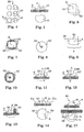
- Fig. 1 is a very schematic illustration of a way of manufacturing optical structures by replication, mainly for clarifying the used terminology.
- the partial images are vertical cross-sections. Where coordinates x, y, z are illustrated in any of the Figures, x and y denote lateral directions, whereas z denotes a vertical direction. Shapes illustrated in Fig. 1 are strongly schematized, and for replication processes discussed further below, specific shapes and details might be required, which are not drawn in Fig. 1 .
- a master M is provided, e.g., by diamond turning or micromachining. Replicating the master M results in a tool T.
- tool T is used as a recombination tool, creating, on a substrate S1 a multitude of replicas, such that a master wafer MW is obtained.
- Master wafer MW can also be referred to as sub-master or wafer-level master.
- a number of structures are formed on substrate S1, which may be distant from each other separated by a gap g, or (not shown) may overlap or partially coincide.
- the structures may comprise a main portion m each and a surrounding portion s surrounding the respective main portion.
- a replication tool R also referred to as wafer-level tool, is obtained, namely by replicating master wafer MW on a substrate S2.
- a replication tool R in a replication process then results in a wafer comprising a multitude of final replicas F on a substrate S3, wherein each of these may, as illustrated in Fig. 1 , comprise a main portion m and a surrounding portion s.
- the final replicas F can in particular be optical structures 50, e.g., wherein each of said main portions is a passive optical component and more particularly a lens such as a plane-convex refractive lens.
- the replication material r for the optical structures will, at least for transparent passive optical components, be a transparent one.
- separation takes place, e.g., using a dicing saw, so as to obtain separate optical structures 50 or separate sets of two or more optical structures.
- Dicing lines are denoted by d.
- the substrates S1, S2, S3 can be, e.g., blank wafers (e.g., glass or polymeric), wherein at least substrate S3 in this case would be a transparent wafer.
- substrates S1, S2, S3 can be, e.g., blank wafers (e.g., glass or polymeric), wherein at least substrate S3 in this case would be a transparent wafer.
- Substrates with transparent portions and one or more (non-transparent) blocking portions are described further below and, in more detail, in particular concerning their manufacture, in the before-mentioned US 2013/0153772 A1 to which it is hereby explicitely referred.
- Fig. 2 illustrates, in a top-view, a portion of a wafer for illustrating a wafer-level method for modifying optical structures 50.
- a multitude of precursor optical structures 5 having a circular aperture are present.
- material is removed from the precursor optical structures 5, thus effeecting a smaller aperture of these.
- the precursor optical strucures 5 may, e.g., be or comprise spherical lenses having a circular lens aperture (which may apply also to other illustrated cases).
- material 59 is removed from the precursor optical structures 5, such that the so-obtained lenses have a lens aperture describing a truncated circle, truncated along a straight line.
- Dicing along other dicing lines such as dicing lines d' may take place, too, for separating the optical structures.
- lines 99 along which material is removed are not lines in the mathematical sense having no width, but they have a width.
- a line 99 along which material is removed from the precursor optical structures 5 coincides with a dicing line d.
- This can be a very efficient process.
- the illustrated process is particularly efficient also for the reason that precursor optical structures present on both sides of line 99 are processed, in the illustrated case even simultaneously.
- Fig. 3 is an illustration, in a top-view, of another wafer-level method for modifying optical structures.
- removal of material of the precursor optical structures 5 does not coincide with cutting through the substrate (dicing), and line 99 along which material is removed from the precursor optical structures 5 does not coincide with dicing lines d or d'.
- the non-shaded portions of precursor optical structures 5 indicate the (aperture) shape of the so-obtained optical structures 50 such as, e.g., truncated lenses.
- Fig. 4 is another illustration, in a top view, of a wafer-level method for modifying optical structures.
- the line 99 is not a straight line, but it is curved. This may be accomplished, e.g., using laser cutting or laser ablation.
- the resulting optical structures 50 may thus have rather peculiar apertures.
- Fig. 5 illustrates an optical structure 50 obtainable in such a way (cf. Fig. 4 ), in two views; on top in a cross-sectional view and below in a(lateral) top view.
- the precursor optical structure may in this case have been a spherical plane-convex lens having an optical axis A coinciding with its axis or rotational symmetry.
- Figs. 6 and 7 illustrate optical structures 50 in a top view which are obtainable from precursor optical structures with circular aperture by removing material 59 therefrom along two and four lines, respectively.
- Fig. 8 illustrates an optical structure 50 obtainable from a precursor optical structure with an elliptic non-circular aperture by removing material 59 therefrom along two lines.
- Fig. 9 shows an example in which only an inner edge is produced, e.g., by point-wise removal of material.
- Material 59 is removed in the center of the initially purely circular aperture; thus, a hole is created in the optical structure.
- the aperture of the so-produced optical structure is ring-shaped. But also differently shaped openings can be produced.
- So-produced inner edges and inner edge surfaces may have various shapes. Techniques suitable for removing portions of material not creating an outer edge are, e.g., laser ablation, micro-machining, milling. These may be applied on wafer level.
- Fig. 10 illustrates an optical structure 50 obtainable from a precursor optical structure with a circular aperture by removing material 59 therefrom creating both, an inner and and outer edge.
- Fig. 11 illustrates an optical structure 50 in a cross-sectional view. It illustrates that a dicing line d along which material is removed from an (in this case plane-concave spherical) precursor optical structure may also leave a portion of the removed material 59 intact. Furthermore, it illustrates that on a substrate S, optical structures and in particular precursor optical structures may be present on both sides, cf. the dotted lines.
- Fig. 12 illustrates optical structures 50 and 50' in a cross-sectional view. These are obtainable simultaneously by dicing or cutting along line 99, starting from a precursor optical structure or passive optical component having a circular or elliptic aperture.
- Fig. 13 illustrates another optical structure 50 in a cross-sectional view.
- material 59 is removed from a precursor optical structure along a line 99 (drawn as a rectangle) without separating substrate S into distinct parts or, at least, without penetrating substrate S.
- Various techniques may accomplish such a task, e.g., micro-machining, laser ablation, sawing, milling.
- the dotted shape symbolizes the possibility to provide optical structures on both sides of substrate S.
- Fig. 14 illustrates an optical structure 50 in two views, cross-section on top, top view below.
- This optical structure 50 may be obtained by removing material (substantially) without removing material from the substrate S.
- the edge surface 5s is indicated.
- This edge surface 5s forms an outside surface of the optical structure 50, and it is in this case a perfectly vertical surface.
- the shape of the edge surface in a vertical cross-section can also be not perfectly straight, e.g., (somewhat) curved.
- Fig. 14 illustrates that it is possible to use substrates S comprising transparent portions t and non-transparent blocking portions b laterally surrounding the transparent portions. This may contribute to improved optical properties, e.g., by impeding undesired optical paths.
- Fig. 15 illustrates an optical device 1a comprising two optical structures 50, 50', in two views, cross-sectional view above, top view below.
- substrates S with transparent portions t and one or more non-transparent blocking portions b laterally surrounding the transparent portions.
- the removed material 59 is indicated, too.
- Edge surface 5s and the corresponding (line-shaped) edge 5e are also indicated.
- Such an optical device 1a may be used, e.g., in multi-channel optical devices such as in proximity sensors and array cameras. It is possible to provide that dicing takes place in a wafer stack. More details concerning such a way of manufacturing can be inferred from the before-mentioned US 2013/0153772 A1 , where this is explained by means of the example of a proximity sensor.
- Fig. 16 illustrates an optical device 1 comprising two optical devices 1a in a cross-sectional view.
- the optical devices 1a may be obtained, e.g., like described for Fig. 11 . These two are mounted, e.g., using pick-and-place, on a substrate S' which may, as illustrated in Fig. 16 , have transparent portions t' and one or more blocking portions b'.
- Fig. 17 is a illustration of a wafer-level-suitable method for modifying optical structures 50, in two views, cross-section on top, top view below.
- the precursor optical structure has in this case a main portion m laterally surrounded by a surrounding portion s.
- Main portion m forms a passive optical component, more particularly a lens.
- Such precursor optical structures may also be used in the other described embodiments in which case surrounding portions would have to be imagined to be present around the passive optical components formed by the illustrated precursor optical structures.
- removal of material 59 may take place along line 99 removing material of surrounding portion s only, leaving main portion m unchanged.
- This may be useful, e.g., when two passive optical components formed by neighboring optical structures (more particularly by their respective main portions) shall be very close to each other, while still ensuring well-defined optical properties.
- surrounding portions of neighboring precursor optical structures may overlap, and subsequently, the material in the overlap region is removed, e.g., for inhibiting the possibility of undesired light propagation through the surrounding portions.
- Fig. 18 very schematically illustrates, in a cross-sectional view, two precursor optical structures 5,5', one in solid lines, one in dotted lines, which are differently distanced from each other.
- the optical structures 5 each comprise a main portion m and a surrounding portion s, the main portion m substantially forming a passive optical component L, more particularly a planar-convex lens.
- a gap g is present between the optical structures 5,5'.
- a certain minum gap distance
- Fig. 18 In the middle third of Fig. 18 , is very schematically illustrated that one can have the surrounding portions overlapping or partially coinciding. This allows to have passive optical components L and their respective optical axes A, A' closer to each other, but usually at the cost of (optically) ill-defined conditions in that overlap region. Ways of remedying this problem by removing material of the optical structures and, more particularly, of the surrounding portions, have been described above, cf., e.g., Figs. 13 and 14 . Furthermore, farther below, ways of manufacturing sets of optical structures with overlap will be described.
- Fig. 18 In the lower third of Fig. 18 , is very schematically illustrated that one can also provide that the main portions overlapp or partially coincide. This allows to have passive optical components L and their respective optical axes A, A' even closer to each other, but again usually at the cost of (optically) ill-defined conditions in that overlap region. Ways of remedying this problem by removing material of the optical structures have been described above, cf., e.g., Figs. 13 and 14 , wherein usually, truncated passive optical components will be produced this way. It is furthermore referred to the farther below described ways of manufacturing sets of optical structures with overlap.
- Truncated optical structures and passive optical components have been described above along with ways of manufacturing the same, cf., e.g., Figs. 2 , 5, 6, 7, 13, 14 .
- Sets of truncated optical structures and passive optical components, respectively, have been described above as well as ways of manufacturing the same, cf., e.g., Figs. 15 and 16 . Further ways of manufacturing truncated optical structures and passive optical components and sets of these will be described farther below.
- Fig. 19 is a illustration of close-by optical structures 5, 5' comprising truncated passive optical components, in a cross-sectional view.
- optical structures 5, 5' with main portions and surrounding portions are illustrated.
- a gap g is provided between the optical structures 5 and 5'. Comparing this to the upper third of Fig. 18 , however clearly shows that a much smaller (lateral) distance between the axes A, A' (and between the two passive optical components) is readily obtained due to the truncated apertures.
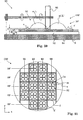
- Fig. 20 very schematically illustrates, in a cross-sectional view, a method for removing material of close-by optical structures 50, 50' of an optics wafer OW, using a dicing saw 90.
- Optics wafer OW can be a wafer with final replicas (cf. Fig. 1 ).
- Dicing saw 90 comprises a rotatable sawing blade or dicing blade 95, and a saw table or dicing chuck 94. Between optics wafer OW and sawing table 95, an intermediate layer 92 such as a dicing tape is present.
- the (adjustable) height of blade 95 is usually referenced with respect to the upper surface of sawing table 94, i.e. it is zero when blade 95 would slightly touch sawing table 94. In usual dicing, the so-referenced height is chosen to be (clearly) above zero (in order to protect the sawing table 94) and to be below the thickness of the intermediate layer 92. This way, it is ensured, in the common way of using a dicing saw, that the wafer to be diced is on the one hand indeed separated into distinct parts and that blade 95 on the other hand does not get into contact with sawing table 94.
- the height h is adjusted differently. It is preset to be larger than the thickness of the intermediate layer 92. Usually, it will be preset to a value within a narrow range (such as plus-minus 30 ⁇ m) around the sum H of the thicknesses of intermediate layer 92 and substrate S, in particular centered about this sum H of heights. The range is referenced as ⁇ in Fig. 20 .
- dicing saw 90 can be efficiently used for the above-described removal of material or separation of optical structures.
- Fig. 21 is a very schematic illustration of a wafer, more particularly of an optics wafer OW like the one illustrated in Fig. 20 , comprising a multitude of sets of optical structures 50, in a top view.
- optics wafer OW comprises a multitude of optical devices 1a comprising a set of four optical structures 50 each.
- each of the four optical structures 50 comprises a main portion m and a surrounding portion s, the latter overlapping.
- Such devices maybe used, e.g., in four-channel sensors such in optical modules for array cameras.
- References 99 and 99' indicate lines along which dicing saw action as described in conjunction with Fig. 20 may be applied. Dicing may subsequently take place along dicing lines d and d', for obtaining separate optical devices 1a.
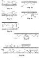
- Fig. 22 shows an optical structure 55 comprising a passive optical component L5, more particularly a spherical lens, in a cross-sectional view.
- a passive optical component L5 more particularly a spherical lens
- Such a (not-truncated) passive optical component L5 having a circular aperture is obtainable using embossing with flow control (cf. explanations further above in the present patent application) using a tool as illustrated in Fig. 23 which will be referred to as precursor tool Tp for reasons which become clear below.
- Fig. 24 shows an optical structure 5 comprising a passive optical component L, more particularly a truncated spherical lens, in a cross-sectional view.
- the lens aperture of lens L of Fig. 24 has a shape different from the one of lens L5 of Fig. 22 , cf. also the double-sided arrows.
- Such a truncated passive optical component L having an aperture describing a circle from which a portion is removed, is obtainable using embossing with flow control (cf. explanations further above in the present patent application) using a tool as the one illustrated in Fig. 25 .
- the surrounding portion s of optical structure 5 has a varied (non-circular) shape (due to the tool T lacking rotational symmetry).
- the tool T is lacking (at least in the appropriate position) a surface portion describing at least one surface of the passive optical component to be produced, more particularly there is no surface portion comprised in tool T which would describe the surface (edge surface) of the truncated passive optical component where the truncated portion of the passive optical component is.
- the tool T of Fig. 25 is obtainable from the precursor tool Tp of Fig. 23 by removing a portion 49 of material thereof, e.g., by laser cutting or sawing.
- Precursor tool Tp may be - where it forms its replication surface - rotationally symmetric and, e.g., manufactured using a corresponding master (cf. Fig. 1 ).
- a surface 46 referred to as flow-stop surface 46 is produced. As indicated in Fig. 25 , an angle ⁇ between this flow-stop surface 46 and the adjacent replication surface portion of tool T is clearly larger than 180°, usually still clearly above 230°. This can be helpful when using tool T in replication with flow control.
- Fig. 26 is an illustration of replication, in a cross-sectional view, for illustrating that replication material may be applied to either the tool T' or the substrate S' or to both, tool and substrate. Tool T' can then be moved towards substrate S' or vice versa, or both move towards the respective other before hardening in the final position.
- two tools of Fig. 25 may be combined on a common holder C, as illustrated in Fig. 27 , wherein the flow-stop surfaces may be inclined, in particular, as illustrated, by different angles ⁇ 1, ⁇ 2.
- all the "partial" tools combined on a common holder for manufacturing sets of passive optical components do not need to be identically shaped, e.g., in particular in case the passive optical components of the set are differently shaped.
- a set of, e.g., two truncated passive optical components such as of a pair of those illustrated in Fig. 24
- Fig. 39 is an illustration of such a way of manufacturing a master wafer MW, in a cross-sectional view.
- the upper portion illustrates that tool T is used for forming first lenses L1 of each set from replication material r applied to substrate S1.
- the lower portion of Fig. 28 illustrates that subsequently, i.e. after all first lenses L1 are produced in a multitude of embossing and hardening steps, the same tool T may be used, but rotated by 180° about a vertical axis, for producing second lenses L2 of the sets. Note that this may be accomplished in such a way that the surrounding portions s of the lenses overlap, cf. the region indicated by the dotted circle in the lower portion of Fig. 28 .
- a tool T for two or more passive optical components of a set may also be obtained from an integrally formed precursor tool, by removing material from such a precursor tool.
- a so-obtained tool may, e.g., look like the one of Fig. 27 , wherein the "partial" tools, i.e. the portions having replication surfaces for different passive optical components of a set, will usually not be distinct parts, but still form a unitary part. This may contribute to an increased alignment precision, in particular concerning mutual position and orientation of the passive optical components.
- the removal of material from the precursor tool may be accomplished using, e.g., milling, laser ablation, micro-machining, cutting using a blade.
- a precursor tool like that may be obtained using replication may be obtained using replication.
- a unitary master may be used allowing to obtain the precursor tool in one replication step.
- masters In the manufacture of truncated passive optical components or of sets of passive optical components, particular masters may be used, in particular such masters which are obtainable from a precursor master by adding material thereto.
- a master it may be desirable to manufacture a master from one or more precursor masters having a spherical surface each, in particular if passive optical components with spherical surfaces shall be manufactured.
- Such precursor masters may be manufactured using, e.g., diamond turning. Cutting off a portion of one or of each of such precursor masters and adding, e.g., a bar at the cut-off edge, at the surface where the material has been removed, can allow to obtain a suitable master.
- a rotationally symmetric replication surface of a precursor master can thus be modified so as to produce a no more rotationally symmetric replication surface of the master.
- Fig. 28 illustrates, in a cross-sectional view, a precursor master Mp.
- Fig. 29 illustrates the situation with material 42 removed from precursor master Mp. Then, material is added, for forming a protruding part 41 of master M.
- Fig. 29 shows an example for a master M comprising the cut-off precursor master with added material of protruding part 41.
- Protruding part 41 forms a surface 44 referred to as protrusion surface which forms an angle ⁇ with the adjacent portion of the replication surface. That angle ⁇ usually is smaller than 150° and rather smaller than 130°.
- Fig. 31 to 33 illustrate how another master M is obtained in a similar way as the one of Fig. 30 .
- the protruding portions 41 can allow to ensure the presence of an empty volume in a tool (or precursor tool) obtained using replication using the master.
- Such an empty volume may fulfill the same or at least similar functions as the space between the two partial tools in Fig. 27 .
- a master like the one of Fig. 30 or the one of Fig. 33 may, e.g., be used for a first and for a subsequent second embossing step in the manufacture of a tool for a set of two passive optical components, in particular wherein the tool is rotated 180° in the second step, like described for tools in conjunction with Fig. 39 .
- Such a multiple-times use of a master may also be accomplished with a master obtained in a different way, e.g., a master forming, at least where it forms its replication surface, a unitary or integrally formed part.
- a master M for two (or generally also even more) passive optical components can be made from two (or more) precursor masters, e.g., such as those of Figs. 28 and 31 .
- An example for such a master M composed of two cut masters plus added material (protruding portion 41) is illustrated in Fig. 34.
- a master M for two (or more passive optical components) as a unitary part (at least in the region where it forms its replication surface), e.g. using micro-machining.
- a master for one passive optical component only can be manufactured as well.
- optical structures and sets of optical structures and devices herein described may find various applications, e.g., in optical or opto-electric devices or modules, in particular in sensor and photographic applications, and especially in multi-channel devices such as array cameras or proximity sensors.
- Fig. 37 illustrates a device 1 which is a two-channel optical module, in a perspective view.
- this module is a proximity sensor or a module for a proximity sensor. But the principles apply, possibly with slight modifications, to many other kinds of modules and devices.
- Module 1 comprises an emission channel 20 from which light, e.g., infrared light can be emitted, and a detecting channel in which light, e.g., infrared light can be detected.
- Composed lenses 8a and 8b are present in channels 20 and 30, respectively, of which passive optical components or lens elements 52 and 53, respectively, are visible. They are comprised in an optics member O.
- a baffle member B On the upper side of optics member O, a baffle member B is arranged, and on the opposite side, a substrate P such as a printed circuit boards is present, which is spaced from optics member O by a spacer member 60.
- the module can be fully manufactured on wafer level, dicing being applied to a wafer stack comprising
- Fig. 38 illustrates a device 10 comprising a two-channel optical module 1 of Fig. 37 .
- Device 10 can be, e.g., a photographic device such as an array camera or a sensor device or a communication device such as a smart phone, or a hand-held electronic device.
- Device 10 comprises a printed circuit board 9 on which module 1 and further in particular electronic components such as an integrated circuit 81 functioning, e.g., as a control unit for module 1 are mounted.
- Module 1 is electrically interconnected with printed circuit board 9, e.g., via solder balls 7, thus providing also an electrical connection to component 81. Accordingly, an electronic circuit 70 is formed.
- a light emitter E such as an LED and a light detector D such as a photo diode are present on substrate P.
- each channel might comprise an image sensor (multi-pixel sensor).
- Composed lens 8a comprises two passive optical components or lens elements 52, 52' which are attached to opposite faces of a transparent portion t present in optics member O in form of a transparent element 6 such as a block of a transparent polymer.
- Composed lens 8b comprises two passive optical components or lens elements 53, 53' which are attached to opposite faces of another transparent portion t present in optics member O.
- hatched portions of the members P, 60, O, B are not transparent, not-hatched ones are transparent.
- openings 4 in spacer member 60 and of transparent regions 3 of baffle member B no solid material is present, but usually merely air or another gas or vacuum.
- Lens element 52' is a truncated passive optical component, and its optical axis A2' is shifted with respect to the optical axis A2 of lens element 52.
- Lens element 53 is a truncated passive optical component, and its optical axis A3 is shifted with respect to the optical axis A3' of lens element 53'.
Landscapes
- Physics & Mathematics (AREA)
- Engineering & Computer Science (AREA)
- Manufacturing & Machinery (AREA)
- General Physics & Mathematics (AREA)
- Optics & Photonics (AREA)
- Mechanical Engineering (AREA)
- Health & Medical Sciences (AREA)
- Ophthalmology & Optometry (AREA)
- Shaping Of Tube Ends By Bending Or Straightening (AREA)
- Eyeglasses (AREA)
- Lenses (AREA)
- Moulds For Moulding Plastics Or The Like (AREA)
Applications Claiming Priority (2)
| Application Number | Priority Date | Filing Date | Title |
|---|---|---|---|
| US201261699666P | 2012-09-11 | 2012-09-11 | |
| PCT/SG2013/000384 WO2014042591A1 (en) | 2012-09-11 | 2013-09-03 | Manufacture of truncated lenses, of pairs of truncated lenses and of corresponding devices |
Publications (3)
| Publication Number | Publication Date |
|---|---|
| EP2895320A1 EP2895320A1 (en) | 2015-07-22 |
| EP2895320A4 EP2895320A4 (en) | 2016-06-15 |
| EP2895320B1 true EP2895320B1 (en) | 2021-12-01 |
Family
ID=50278538
Family Applications (1)
| Application Number | Title | Priority Date | Filing Date |
|---|---|---|---|
| EP13837476.4A Active EP2895320B1 (en) | 2012-09-11 | 2013-09-03 | Method of manufacturing truncated lenses |
Country Status (8)
| Country | Link |
|---|---|
| US (1) | US10377094B2 (enExample) |
| EP (1) | EP2895320B1 (enExample) |
| JP (1) | JP2015534107A (enExample) |
| KR (1) | KR102086187B1 (enExample) |
| CN (3) | CN107479119A (enExample) |
| SG (2) | SG11201501695PA (enExample) |
| TW (2) | TWI648554B (enExample) |
| WO (1) | WO2014042591A1 (enExample) |
Families Citing this family (9)
| Publication number | Priority date | Publication date | Assignee | Title |
|---|---|---|---|---|
| US9169287B2 (en) | 2013-03-15 | 2015-10-27 | Massachusetts Institute Of Technology | Solid phase peptide synthesis processes and associated systems |
| CN106573460B (zh) | 2014-05-16 | 2019-11-29 | 新加坡恒立私人有限公司 | 装置、特别是光学装置的晶片级制造 |
| WO2015174929A1 (en) | 2014-05-16 | 2015-11-19 | Heptagon Micro Optics Pte. Ltd. | Manufacture of optical elements by replication and corresponding replication tools and optical devices |
| EP3349775B1 (en) * | 2015-09-17 | 2021-12-01 | Massachusetts Institute of Technology | Solid phase peptide synthesis methods and associated systems |
| NL2016689B1 (en) * | 2016-04-28 | 2017-11-20 | Anteryon Wafer Optics B V | Replication tool |
| JP2022083016A (ja) * | 2020-11-24 | 2022-06-03 | Agc株式会社 | 光学素子 |
| KR102607878B1 (ko) * | 2021-09-17 | 2023-11-30 | 현대모비스 주식회사 | 엘이디 모듈 및 이를 포함하는 차량 |
| US20240230965A9 (en) * | 2022-10-24 | 2024-07-11 | Viavi Solutions Inc. | Die including a non-rectangular shaped optical material and methods of manufacture |
| DE102023123813A1 (de) * | 2023-09-05 | 2025-03-06 | Valeo Detection Systems GmbH | Linse für ein optisches sensor-system sowie verfahren zur herstellung |
Family Cites Families (29)
| Publication number | Priority date | Publication date | Assignee | Title |
|---|---|---|---|---|
| US3270383A (en) * | 1963-06-24 | 1966-09-06 | Gen Motors Corp | Method of die casting |
| US4407766A (en) * | 1981-05-26 | 1983-10-04 | National Patent Development Corporation | Molds and procedure for producing truncated contact lenses |
| JPS58171021A (ja) * | 1982-03-31 | 1983-10-07 | Fujitsu Ltd | アレイ構造を有するレンズとその製造方法 |
| US5536455A (en) | 1994-01-03 | 1996-07-16 | Omron Corporation | Method of manufacturing lens array |
| US5759457A (en) * | 1995-02-24 | 1998-06-02 | Matsushita Electric Industrial Co., Ltd. | Method for manufacturing an optical element |
| JPH10123306A (ja) * | 1996-10-18 | 1998-05-15 | Nikon Corp | プラスチックレンズおよびその製造方法 |
| US7267846B2 (en) | 1999-11-01 | 2007-09-11 | Praful Doshi | Tinted lenses and methods of manufacture |
| WO2002016975A2 (en) * | 2000-08-21 | 2002-02-28 | Siwave, Inc. | Lens arrays and methods of making the lens array |
| US6739766B2 (en) * | 2001-12-17 | 2004-05-25 | Stratos International, Inc. | Lens array for use in parallel optics modules for fiber optics communications |
| EP1443344A1 (en) * | 2003-01-29 | 2004-08-04 | Heptagon Oy | Manufacturing micro-structured elements |
| EP1542074A1 (en) * | 2003-12-11 | 2005-06-15 | Heptagon OY | Manufacturing a replication tool, sub-master or replica |
| JP4380522B2 (ja) | 2004-02-06 | 2009-12-09 | 日本ビクター株式会社 | マイクロレンズアレイ用複製型の製造方法 |
| KR100693927B1 (ko) | 2005-02-03 | 2007-03-12 | 삼성전자주식회사 | 마이크로 렌즈 제조방법, 마이크로 렌즈 어레이 제조방법및 이미지 센서 제조방법 |
| US7880794B2 (en) | 2005-03-24 | 2011-02-01 | Panasonic Corporation | Imaging device including a plurality of lens elements and a imaging sensor |
| US20070216048A1 (en) * | 2006-03-20 | 2007-09-20 | Heptagon Oy | Manufacturing optical elements |
| US20100072640A1 (en) * | 2006-06-09 | 2010-03-25 | Heptagon Oy | Manufacturing a replication tool, sub-master or replica |
| US20080246171A1 (en) | 2006-09-27 | 2008-10-09 | Berckmiller Gregory L | Chilled injection molding during ophthalmic lens manufacture |
| EP2070636B1 (en) * | 2006-10-04 | 2015-08-05 | Hamamatsu Photonics K.K. | Laser processing method |
| US9153614B2 (en) | 2007-08-15 | 2015-10-06 | Micron Technology, Inc. | Method and apparatus for lens alignment for optically sensitive devices and systems implementing same |
| JP2009209012A (ja) * | 2008-03-05 | 2009-09-17 | Olympus Corp | 成形型および成形型の製造方法 |
| JP2009302483A (ja) * | 2008-06-17 | 2009-12-24 | Panasonic Corp | 固体撮像装置及びその製造方法 |
| US7916396B2 (en) * | 2008-06-27 | 2011-03-29 | Micron Technology, Inc. | Lens master devices, lens structures, imaging devices, and methods and apparatuses of making the same |
| KR101690643B1 (ko) * | 2008-12-05 | 2016-12-28 | 리퀴디아 테크놀로지스 인코포레이티드 | 패턴 재료 제조 방법 |
| CN101870151A (zh) * | 2009-04-27 | 2010-10-27 | 鸿富锦精密工业(深圳)有限公司 | 光学元件的制造方法及压印模具 |
| TW201109164A (en) * | 2009-09-11 | 2011-03-16 | E Pin Optical Industry Co Ltd | Stacked disk-shaped optical lens array, stacked lens module and their method of manufacturing thereof |
| JP5352392B2 (ja) | 2009-09-14 | 2013-11-27 | 富士フイルム株式会社 | ウェハレベルレンズアレイの製造方法、ウェハレベルレンズアレイ、レンズモジュール及び撮像ユニット |
| KR20120087904A (ko) | 2009-09-29 | 2012-08-07 | 코니카 미놀타 어드밴스드 레이어즈 인코포레이티드 | 렌즈 및 렌즈의 가공 방법 |
| JP2011249445A (ja) * | 2010-05-25 | 2011-12-08 | Fujifilm Corp | 固体撮像素子の製造方法 |
| CN201788296U (zh) * | 2010-08-06 | 2011-04-06 | 南通天鸿镭射科技有限公司 | 一种液晶平面显示器用增亮膜 |
-
2013
- 2013-09-03 CN CN201710789204.1A patent/CN107479119A/zh active Pending
- 2013-09-03 US US14/426,472 patent/US10377094B2/en active Active
- 2013-09-03 SG SG11201501695PA patent/SG11201501695PA/en unknown
- 2013-09-03 CN CN201710789221.5A patent/CN107490815B/zh active Active
- 2013-09-03 WO PCT/SG2013/000384 patent/WO2014042591A1/en not_active Ceased
- 2013-09-03 EP EP13837476.4A patent/EP2895320B1/en active Active
- 2013-09-03 SG SG10201701641RA patent/SG10201701641RA/en unknown
- 2013-09-03 JP JP2015531046A patent/JP2015534107A/ja active Pending
- 2013-09-03 KR KR1020157008344A patent/KR102086187B1/ko active Active
- 2013-09-03 CN CN201380058510.8A patent/CN104822517B/zh active Active
- 2013-09-05 TW TW106134759A patent/TWI648554B/zh active
- 2013-09-05 TW TW102131991A patent/TWI610088B/zh active
Non-Patent Citations (1)
| Title |
|---|
| None * |
Also Published As
| Publication number | Publication date |
|---|---|
| KR102086187B1 (ko) | 2020-03-06 |
| KR20150082193A (ko) | 2015-07-15 |
| CN104822517A (zh) | 2015-08-05 |
| TW201415072A (zh) | 2014-04-16 |
| CN107490815B (zh) | 2020-03-17 |
| JP2015534107A (ja) | 2015-11-26 |
| US10377094B2 (en) | 2019-08-13 |
| CN107490815A (zh) | 2017-12-19 |
| TWI648554B (zh) | 2019-01-21 |
| CN104822517B (zh) | 2017-10-03 |
| TWI610088B (zh) | 2018-01-01 |
| SG10201701641RA (en) | 2017-04-27 |
| TW201804206A (zh) | 2018-02-01 |
| EP2895320A4 (en) | 2016-06-15 |
| SG11201501695PA (en) | 2015-04-29 |
| EP2895320A1 (en) | 2015-07-22 |
| WO2014042591A1 (en) | 2014-03-20 |
| US20150217524A1 (en) | 2015-08-06 |
| CN107479119A (zh) | 2017-12-15 |
Similar Documents
| Publication | Publication Date | Title |
|---|---|---|
| EP2895320B1 (en) | Method of manufacturing truncated lenses | |
| EP2748854B1 (en) | Wafer-level fabrication of optical devices with front focal length correction | |
| KR101966478B1 (ko) | 수동 광학 부품을 제조하기 위한 방법 및 그것을 포함하는 장치 | |
| CN1947254A (zh) | 光电子器件上的微光学元件 | |
| JP6987907B2 (ja) | 装置の、特に光学装置のウェーハレベル方法 | |
| TWI557791B (zh) | 用於物體和對應半加工產品之晶圓平面製造的方法 | |
| CN108076671B (zh) | 包括直接粘附到衬底的间隔件的光学组件 | |
| EP2939053B1 (en) | Fabrication of optical elements | |
| US10403671B2 (en) | Wafer-level optical modules and methods for manufacturing the same | |
| HK1212044B (en) | Suspended lens systems and wafer-level methods for manufacturing the same | |
| HK1212044A1 (en) | Suspended lens systems and wafer-level methods for manufacturing the same |
Legal Events
| Date | Code | Title | Description |
|---|---|---|---|
| PUAI | Public reference made under article 153(3) epc to a published international application that has entered the european phase |
Free format text: ORIGINAL CODE: 0009012 |
|
| 17P | Request for examination filed |
Effective date: 20150304 |
|
| AK | Designated contracting states |
Kind code of ref document: A1 Designated state(s): AL AT BE BG CH CY CZ DE DK EE ES FI FR GB GR HR HU IE IS IT LI LT LU LV MC MK MT NL NO PL PT RO RS SE SI SK SM TR |
|
| AX | Request for extension of the european patent |
Extension state: BA ME |
|
| DAX | Request for extension of the european patent (deleted) | ||
| RA4 | Supplementary search report drawn up and despatched (corrected) |
Effective date: 20160517 |
|
| RIC1 | Information provided on ipc code assigned before grant |
Ipc: G02B 3/00 20060101ALI20160510BHEP Ipc: B29C 33/00 20060101ALI20160510BHEP Ipc: B29D 11/00 20060101AFI20160510BHEP |
|
| STAA | Information on the status of an ep patent application or granted ep patent |
Free format text: STATUS: EXAMINATION IS IN PROGRESS |
|
| 17Q | First examination report despatched |
Effective date: 20200422 |
|
| GRAP | Despatch of communication of intention to grant a patent |
Free format text: ORIGINAL CODE: EPIDOSNIGR1 |
|
| STAA | Information on the status of an ep patent application or granted ep patent |
Free format text: STATUS: GRANT OF PATENT IS INTENDED |
|
| INTG | Intention to grant announced |
Effective date: 20210618 |
|
| GRAS | Grant fee paid |
Free format text: ORIGINAL CODE: EPIDOSNIGR3 |
|
| GRAA | (expected) grant |
Free format text: ORIGINAL CODE: 0009210 |
|
| STAA | Information on the status of an ep patent application or granted ep patent |
Free format text: STATUS: THE PATENT HAS BEEN GRANTED |
|
| AK | Designated contracting states |
Kind code of ref document: B1 Designated state(s): AL AT BE BG CH CY CZ DE DK EE ES FI FR GB GR HR HU IE IS IT LI LT LU LV MC MK MT NL NO PL PT RO RS SE SI SK SM TR |
|
| REG | Reference to a national code |
Ref country code: GB Ref legal event code: FG4D |
|
| REG | Reference to a national code |
Ref country code: AT Ref legal event code: REF Ref document number: 1451358 Country of ref document: AT Kind code of ref document: T Effective date: 20211215 Ref country code: CH Ref legal event code: EP |
|
| REG | Reference to a national code |
Ref country code: IE Ref legal event code: FG4D |
|
| REG | Reference to a national code |
Ref country code: DE Ref legal event code: R096 Ref document number: 602013080287 Country of ref document: DE |
|
| REG | Reference to a national code |
Ref country code: LT Ref legal event code: MG9D |
|
| REG | Reference to a national code |
Ref country code: NL Ref legal event code: MP Effective date: 20211201 |
|
| REG | Reference to a national code |
Ref country code: AT Ref legal event code: MK05 Ref document number: 1451358 Country of ref document: AT Kind code of ref document: T Effective date: 20211201 |
|
| PG25 | Lapsed in a contracting state [announced via postgrant information from national office to epo] |
Ref country code: RS Free format text: LAPSE BECAUSE OF FAILURE TO SUBMIT A TRANSLATION OF THE DESCRIPTION OR TO PAY THE FEE WITHIN THE PRESCRIBED TIME-LIMIT Effective date: 20211201 Ref country code: LT Free format text: LAPSE BECAUSE OF FAILURE TO SUBMIT A TRANSLATION OF THE DESCRIPTION OR TO PAY THE FEE WITHIN THE PRESCRIBED TIME-LIMIT Effective date: 20211201 Ref country code: FI Free format text: LAPSE BECAUSE OF FAILURE TO SUBMIT A TRANSLATION OF THE DESCRIPTION OR TO PAY THE FEE WITHIN THE PRESCRIBED TIME-LIMIT Effective date: 20211201 Ref country code: BG Free format text: LAPSE BECAUSE OF FAILURE TO SUBMIT A TRANSLATION OF THE DESCRIPTION OR TO PAY THE FEE WITHIN THE PRESCRIBED TIME-LIMIT Effective date: 20220301 Ref country code: AT Free format text: LAPSE BECAUSE OF FAILURE TO SUBMIT A TRANSLATION OF THE DESCRIPTION OR TO PAY THE FEE WITHIN THE PRESCRIBED TIME-LIMIT Effective date: 20211201 |
|
| PG25 | Lapsed in a contracting state [announced via postgrant information from national office to epo] |
Ref country code: SE Free format text: LAPSE BECAUSE OF FAILURE TO SUBMIT A TRANSLATION OF THE DESCRIPTION OR TO PAY THE FEE WITHIN THE PRESCRIBED TIME-LIMIT Effective date: 20211201 Ref country code: PL Free format text: LAPSE BECAUSE OF FAILURE TO SUBMIT A TRANSLATION OF THE DESCRIPTION OR TO PAY THE FEE WITHIN THE PRESCRIBED TIME-LIMIT Effective date: 20211201 Ref country code: NO Free format text: LAPSE BECAUSE OF FAILURE TO SUBMIT A TRANSLATION OF THE DESCRIPTION OR TO PAY THE FEE WITHIN THE PRESCRIBED TIME-LIMIT Effective date: 20220301 Ref country code: LV Free format text: LAPSE BECAUSE OF FAILURE TO SUBMIT A TRANSLATION OF THE DESCRIPTION OR TO PAY THE FEE WITHIN THE PRESCRIBED TIME-LIMIT Effective date: 20211201 Ref country code: HR Free format text: LAPSE BECAUSE OF FAILURE TO SUBMIT A TRANSLATION OF THE DESCRIPTION OR TO PAY THE FEE WITHIN THE PRESCRIBED TIME-LIMIT Effective date: 20211201 Ref country code: GR Free format text: LAPSE BECAUSE OF FAILURE TO SUBMIT A TRANSLATION OF THE DESCRIPTION OR TO PAY THE FEE WITHIN THE PRESCRIBED TIME-LIMIT Effective date: 20220302 Ref country code: ES Free format text: LAPSE BECAUSE OF FAILURE TO SUBMIT A TRANSLATION OF THE DESCRIPTION OR TO PAY THE FEE WITHIN THE PRESCRIBED TIME-LIMIT Effective date: 20211201 |
|
| PG25 | Lapsed in a contracting state [announced via postgrant information from national office to epo] |
Ref country code: NL Free format text: LAPSE BECAUSE OF FAILURE TO SUBMIT A TRANSLATION OF THE DESCRIPTION OR TO PAY THE FEE WITHIN THE PRESCRIBED TIME-LIMIT Effective date: 20211201 |
|
| PG25 | Lapsed in a contracting state [announced via postgrant information from national office to epo] |
Ref country code: SM Free format text: LAPSE BECAUSE OF FAILURE TO SUBMIT A TRANSLATION OF THE DESCRIPTION OR TO PAY THE FEE WITHIN THE PRESCRIBED TIME-LIMIT Effective date: 20211201 Ref country code: SK Free format text: LAPSE BECAUSE OF FAILURE TO SUBMIT A TRANSLATION OF THE DESCRIPTION OR TO PAY THE FEE WITHIN THE PRESCRIBED TIME-LIMIT Effective date: 20211201 Ref country code: RO Free format text: LAPSE BECAUSE OF FAILURE TO SUBMIT A TRANSLATION OF THE DESCRIPTION OR TO PAY THE FEE WITHIN THE PRESCRIBED TIME-LIMIT Effective date: 20211201 Ref country code: PT Free format text: LAPSE BECAUSE OF FAILURE TO SUBMIT A TRANSLATION OF THE DESCRIPTION OR TO PAY THE FEE WITHIN THE PRESCRIBED TIME-LIMIT Effective date: 20220401 Ref country code: EE Free format text: LAPSE BECAUSE OF FAILURE TO SUBMIT A TRANSLATION OF THE DESCRIPTION OR TO PAY THE FEE WITHIN THE PRESCRIBED TIME-LIMIT Effective date: 20211201 Ref country code: CZ Free format text: LAPSE BECAUSE OF FAILURE TO SUBMIT A TRANSLATION OF THE DESCRIPTION OR TO PAY THE FEE WITHIN THE PRESCRIBED TIME-LIMIT Effective date: 20211201 |
|
| REG | Reference to a national code |
Ref country code: DE Ref legal event code: R097 Ref document number: 602013080287 Country of ref document: DE |
|
| PG25 | Lapsed in a contracting state [announced via postgrant information from national office to epo] |
Ref country code: IS Free format text: LAPSE BECAUSE OF FAILURE TO SUBMIT A TRANSLATION OF THE DESCRIPTION OR TO PAY THE FEE WITHIN THE PRESCRIBED TIME-LIMIT Effective date: 20220401 |
|
| PLBE | No opposition filed within time limit |
Free format text: ORIGINAL CODE: 0009261 |
|
| STAA | Information on the status of an ep patent application or granted ep patent |
Free format text: STATUS: NO OPPOSITION FILED WITHIN TIME LIMIT |
|
| PG25 | Lapsed in a contracting state [announced via postgrant information from national office to epo] |
Ref country code: DK Free format text: LAPSE BECAUSE OF FAILURE TO SUBMIT A TRANSLATION OF THE DESCRIPTION OR TO PAY THE FEE WITHIN THE PRESCRIBED TIME-LIMIT Effective date: 20211201 Ref country code: AL Free format text: LAPSE BECAUSE OF FAILURE TO SUBMIT A TRANSLATION OF THE DESCRIPTION OR TO PAY THE FEE WITHIN THE PRESCRIBED TIME-LIMIT Effective date: 20211201 |
|
| 26N | No opposition filed |
Effective date: 20220902 |
|
| PG25 | Lapsed in a contracting state [announced via postgrant information from national office to epo] |
Ref country code: SI Free format text: LAPSE BECAUSE OF FAILURE TO SUBMIT A TRANSLATION OF THE DESCRIPTION OR TO PAY THE FEE WITHIN THE PRESCRIBED TIME-LIMIT Effective date: 20211201 |
|
| PG25 | Lapsed in a contracting state [announced via postgrant information from national office to epo] |
Ref country code: MC Free format text: LAPSE BECAUSE OF FAILURE TO SUBMIT A TRANSLATION OF THE DESCRIPTION OR TO PAY THE FEE WITHIN THE PRESCRIBED TIME-LIMIT Effective date: 20211201 |
|
| REG | Reference to a national code |
Ref country code: CH Ref legal event code: PL |
|
| GBPC | Gb: european patent ceased through non-payment of renewal fee |
Effective date: 20220903 |
|
| REG | Reference to a national code |
Ref country code: BE Ref legal event code: MM Effective date: 20220930 |
|
| PG25 | Lapsed in a contracting state [announced via postgrant information from national office to epo] |
Ref country code: IT Free format text: LAPSE BECAUSE OF FAILURE TO SUBMIT A TRANSLATION OF THE DESCRIPTION OR TO PAY THE FEE WITHIN THE PRESCRIBED TIME-LIMIT Effective date: 20211201 |
|
| PG25 | Lapsed in a contracting state [announced via postgrant information from national office to epo] |
Ref country code: LU Free format text: LAPSE BECAUSE OF NON-PAYMENT OF DUE FEES Effective date: 20220903 |
|
| PG25 | Lapsed in a contracting state [announced via postgrant information from national office to epo] |
Ref country code: LI Free format text: LAPSE BECAUSE OF NON-PAYMENT OF DUE FEES Effective date: 20220930 Ref country code: IE Free format text: LAPSE BECAUSE OF NON-PAYMENT OF DUE FEES Effective date: 20220903 Ref country code: CH Free format text: LAPSE BECAUSE OF NON-PAYMENT OF DUE FEES Effective date: 20220930 |
|
| PG25 | Lapsed in a contracting state [announced via postgrant information from national office to epo] |
Ref country code: BE Free format text: LAPSE BECAUSE OF NON-PAYMENT OF DUE FEES Effective date: 20220930 |
|
| P01 | Opt-out of the competence of the unified patent court (upc) registered |
Effective date: 20230825 |
|
| PG25 | Lapsed in a contracting state [announced via postgrant information from national office to epo] |
Ref country code: GB Free format text: LAPSE BECAUSE OF NON-PAYMENT OF DUE FEES Effective date: 20220903 |
|
| PG25 | Lapsed in a contracting state [announced via postgrant information from national office to epo] |
Ref country code: HU Free format text: LAPSE BECAUSE OF FAILURE TO SUBMIT A TRANSLATION OF THE DESCRIPTION OR TO PAY THE FEE WITHIN THE PRESCRIBED TIME-LIMIT; INVALID AB INITIO Effective date: 20130903 |
|
| PG25 | Lapsed in a contracting state [announced via postgrant information from national office to epo] |
Ref country code: CY Free format text: LAPSE BECAUSE OF FAILURE TO SUBMIT A TRANSLATION OF THE DESCRIPTION OR TO PAY THE FEE WITHIN THE PRESCRIBED TIME-LIMIT Effective date: 20211201 |
|
| PG25 | Lapsed in a contracting state [announced via postgrant information from national office to epo] |
Ref country code: MK Free format text: LAPSE BECAUSE OF FAILURE TO SUBMIT A TRANSLATION OF THE DESCRIPTION OR TO PAY THE FEE WITHIN THE PRESCRIBED TIME-LIMIT Effective date: 20211201 |
|
| PG25 | Lapsed in a contracting state [announced via postgrant information from national office to epo] |
Ref country code: TR Free format text: LAPSE BECAUSE OF FAILURE TO SUBMIT A TRANSLATION OF THE DESCRIPTION OR TO PAY THE FEE WITHIN THE PRESCRIBED TIME-LIMIT Effective date: 20211201 |
|
| PG25 | Lapsed in a contracting state [announced via postgrant information from national office to epo] |
Ref country code: MT Free format text: LAPSE BECAUSE OF FAILURE TO SUBMIT A TRANSLATION OF THE DESCRIPTION OR TO PAY THE FEE WITHIN THE PRESCRIBED TIME-LIMIT Effective date: 20211201 |
|
| REG | Reference to a national code |
Ref country code: DE Ref legal event code: R082 Ref document number: 602013080287 Country of ref document: DE Representative=s name: LORENZ SEIDLER GOSSEL RECHTSANWAELTE PATENTANW, DE Ref country code: DE Ref legal event code: R081 Ref document number: 602013080287 Country of ref document: DE Owner name: FOCUSLIGHT SINGAPORE PTE. LTD., SG Free format text: FORMER OWNER: HEPTAGON MICRO OPTICS PTE. LTD., SINGAPORE, SG |
|
| PGFP | Annual fee paid to national office [announced via postgrant information from national office to epo] |
Ref country code: DE Payment date: 20250916 Year of fee payment: 13 |
|
| PGFP | Annual fee paid to national office [announced via postgrant information from national office to epo] |
Ref country code: FR Payment date: 20250929 Year of fee payment: 13 |