EP2871714B1 - Printed antenna and terminal device - Google Patents
Printed antenna and terminal device Download PDFInfo
- Publication number
- EP2871714B1 EP2871714B1 EP14814654.1A EP14814654A EP2871714B1 EP 2871714 B1 EP2871714 B1 EP 2871714B1 EP 14814654 A EP14814654 A EP 14814654A EP 2871714 B1 EP2871714 B1 EP 2871714B1
- Authority
- EP
- European Patent Office
- Prior art keywords
- antenna
- antenna pattern
- printed
- terminal device
- pattern
- Prior art date
- Legal status (The legal status is an assumption and is not a legal conclusion. Google has not performed a legal analysis and makes no representation as to the accuracy of the status listed.)
- Active
Links
- 238000003466 welding Methods 0.000 claims description 28
- 238000004891 communication Methods 0.000 claims description 17
- 239000003990 capacitor Substances 0.000 claims description 5
- 238000010586 diagram Methods 0.000 description 11
- 238000000034 method Methods 0.000 description 7
- 230000005855 radiation Effects 0.000 description 7
- 230000008878 coupling Effects 0.000 description 5
- 238000010168 coupling process Methods 0.000 description 5
- 238000005859 coupling reaction Methods 0.000 description 5
- 238000005516 engineering process Methods 0.000 description 5
- 230000010354 integration Effects 0.000 description 4
- 239000002184 metal Substances 0.000 description 2
- 238000013459 approach Methods 0.000 description 1
- 230000001419 dependent effect Effects 0.000 description 1
- 238000013461 design Methods 0.000 description 1
- 238000011161 development Methods 0.000 description 1
- 230000000694 effects Effects 0.000 description 1
- 230000007774 longterm Effects 0.000 description 1
- 238000010295 mobile communication Methods 0.000 description 1
- 230000003287 optical effect Effects 0.000 description 1
- 238000007639 printing Methods 0.000 description 1
- 238000012545 processing Methods 0.000 description 1
Images


Classifications
-
- H—ELECTRICITY
- H01—ELECTRIC ELEMENTS
- H01Q—ANTENNAS, i.e. RADIO AERIALS
- H01Q9/00—Electrically-short antennas having dimensions not more than twice the operating wavelength and consisting of conductive active radiating elements
- H01Q9/04—Resonant antennas
- H01Q9/0407—Substantially flat resonant element parallel to ground plane, e.g. patch antenna
-
- H—ELECTRICITY
- H01—ELECTRIC ELEMENTS
- H01Q—ANTENNAS, i.e. RADIO AERIALS
- H01Q1/00—Details of, or arrangements associated with, antennas
- H01Q1/36—Structural form of radiating elements, e.g. cone, spiral, umbrella; Particular materials used therewith
- H01Q1/38—Structural form of radiating elements, e.g. cone, spiral, umbrella; Particular materials used therewith formed by a conductive layer on an insulating support
-
- H—ELECTRICITY
- H01—ELECTRIC ELEMENTS
- H01Q—ANTENNAS, i.e. RADIO AERIALS
- H01Q5/00—Arrangements for simultaneous operation of antennas on two or more different wavebands, e.g. dual-band or multi-band arrangements
- H01Q5/30—Arrangements for providing operation on different wavebands
- H01Q5/307—Individual or coupled radiating elements, each element being fed in an unspecified way
- H01Q5/314—Individual or coupled radiating elements, each element being fed in an unspecified way using frequency dependent circuits or components, e.g. trap circuits or capacitors
- H01Q5/321—Individual or coupled radiating elements, each element being fed in an unspecified way using frequency dependent circuits or components, e.g. trap circuits or capacitors within a radiating element or between connected radiating elements
-
- H—ELECTRICITY
- H01—ELECTRIC ELEMENTS
- H01Q—ANTENNAS, i.e. RADIO AERIALS
- H01Q5/00—Arrangements for simultaneous operation of antennas on two or more different wavebands, e.g. dual-band or multi-band arrangements
- H01Q5/30—Arrangements for providing operation on different wavebands
- H01Q5/307—Individual or coupled radiating elements, each element being fed in an unspecified way
- H01Q5/342—Individual or coupled radiating elements, each element being fed in an unspecified way for different propagation modes
- H01Q5/357—Individual or coupled radiating elements, each element being fed in an unspecified way for different propagation modes using a single feed point
- H01Q5/364—Creating multiple current paths
- H01Q5/371—Branching current paths
Definitions
- the present invention relates to the field of wireless communications technologies, and in particular, to a printed antenna and a terminal device.
- LTE Long Term Evolution
- 3G 3rd Generation
- a conventional antenna cannot satisfy a requirement for a sufficient bandwidth.
- antenna efficiency (a ratio of power radiated by an antenna to active power input into the antenna, where a numerical value of the ratio is constantly less than 1) cannot be too low (at least greater than 35% at the frequency band of 698MHz to 960 MHz, and at least greater than 45% at the frequency band of 1710MHz to 2690 MHz).
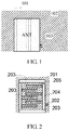
- FIG. 1 a structure of a terminal antenna is shown in FIG. 1 , where 101 is a PCB (Printed Circuit Board, printed circuit board), 102 is an antenna pattern, and 103 is a signal feed-in point.
- the signal feed-in point is a connection point of an antenna and a connection point of a radio frequency circuit to feed in or feed out a signal.
- a size of the antenna is further reduced by means of printing the antenna on the PCB, but the power of the antenna is low and the bandwidth is narrow.
- a radio frequency circuit with an antenna must implement double resonance of a high frequency and a low frequency by adding a matching circuit, which may increase a resonance point, but cannot improve efficiency of the antenna, and also restricts improvement of the bandwidth.
- an objective of the present invention is to provide a printed antenna and a terminal device, so that in a case in which an external device, such as an inductor or a capacitor, does not need to be connected to perform matching, a bandwidth of an antenna satisfies a requirement of a current LTE full frequency band, especially broadening a low frequency bandwidth of the antenna. Further, efficiency of the antenna at a high frequency band is improved. Therefore, the present invention provides a printed antenna with the features of claim 1 and a terminal device with the features of claim 3. Optional features are set out in the dependent claims.
- a bandwidth of a printed antenna satisfies a requirement of a current LTE full frequency band in a case in which a matching circuit does not need to be added, especially, a low frequency bandwidth of the antenna is broadened, which resolves a problem that a high frequency bandwidth is too broad, and meanwhile improves efficiency of the antenna at the full frequency band.
- the printed antenna is printed on a printed circuit board, which requires no or few matching devices, thereby effectively reducing costs.
- a printed antenna is used to perform communication.
- a matching circuit needs to be added to implement double resonance of a high frequency and a low frequency.
- a size of the antenna cannot be reduced, and further, a low frequency bandwidth of the printed antenna cannot satisfy an LTE communications requirement, which leads to low efficiency of the antenna.
- Embodiments of the present invention provide a printed antenna that can satisfy a requirement of a current LTE full frequency band.
- a low frequency bandwidth of the antenna is broadened, which resolves a problem that a high frequency bandwidth is too broad, and meanwhile improves efficiency of the antenna at the full frequency band.
- the printed antenna is printed on a printed circuit board, which requires no or few matching devices, thereby effectively reducing costs.
- FIG. 2 is a schematic structural diagram of a printed antenna according to an embodiment of the present invention.
- the printed antenna includes: a printed circuit board 201, an antenna pattern, and a signal feed-in point 202, where the antenna pattern is printed on a front surface of the printed circuit board 201.
- the antenna pattern includes: a first antenna pattern 203, a second antenna pattern 204, and a third antenna pattern 205.
- the signal feed-in point 202 is connected to the second antenna pattern 204.
- One end of a side, which is laid out along an edge of the printed circuit board 201, of the first antenna pattern 203 is connected to the second antenna pattern 204.
- the second antenna pattern 204 is vertically laid out in parallel to an edge of the printed circuit board 201, where the second antenna pattern 204 and the first antenna pattern 203 form a non-closed rectangular.
- the third antenna pattern 205 includes a first part 2051 and a second part 2052, where one end of the first part 2051 of the third antenna pattern 205 is connected to the first antenna pattern 203, and one end of the second part 2052 of the third antenna pattern 205 is connected to the second antenna pattern 204, and the first part 2051 and the second part 2052 are arranged in parallel in the non-closed rectangle.
- one side of the first antenna pattern 203 is laid out along an edge of the printed circuit board 201, and other sides of the antenna pattern 203 are laid out around a metal ground of the printed circuit board 201.
- the signal feed-in point 202 is connected to the second antenna pattern 204, and is disposed near the edge of the printed circuit board 201. Electromagnetic coupling is generated between the first antenna pattern 203 and the metal ground of the printed circuit board 201 and a low frequency band of an antenna radiation bandwidth is generated.
- a specific low frequency band may be 698 MHz to 960 MHz.
- a length of the first antenna pattern 203 may be set, and a width of a gap between the first antenna pattern 203 and the printed circuit board 201 may also be set.
- the second antenna pattern 204 is vertically laid out in parallel to the edge of the printed circuit board 201, and one end of the side, which is laid out along the edge of the printed circuit board 201, of the first antenna pattern 203 is connected to the second antenna pattern 204, where the second antenna pattern 204 and the first antenna pattern 203 form a non-closed rectangular.
- the second antenna pattern 204 generates a high frequency band of the antenna radiation bandwidth by means of radiation, and a specific high frequency band may be 2 GHz to 3 GHz.
- a length of the second antenna pattern 204 may be set, and a width of a gap between the second antenna pattern 204 and the printed circuit board 201 may also be set.
- the third antenna pattern 205 includes a first part 2051 and a second part 2052, where one end of the first part 2051 is connected to the first antenna pattern 203, and one end of the second part 2052 is connected to the second antenna pattern 204, and the first part 2051 and the second part 2052 are arranged in parallel in the non-closed rectangle.
- the first part 2051 and the second part 2052 which are alternately arranged in parallel, of the third antenna pattern 205 generate a high frequency band of the antenna radiation bandwidth, where specifically, the high frequency band may be 1.71 GHz to 2.17 GHz.
- a width, length, shape or quantity of the first part 2051 of the third antenna pattern 205 may be set to a fixed value, and a width, length, shape, or quantity of the second part 2052 of the third antenna pattern 205 may also be set to a fixed value.
- the printed antenna further includes a welding element, where the welding element includes at least one of the following: an inductor, a capacitor, a resistor, or the like.
- the welding element includes at least one of the following: an inductor, a capacitor, a resistor, or the like.
- One end of the first part 2051 of the third antenna pattern 205 is connected to the first antenna pattern 203 by using the welding element, and/or one end of the second part 2052 of the third antenna pattern 205 is connected to the second antenna pattern 204 by using the welding element.
- the third antenna pattern 205 includes a first part 2051 and a second part 2052.
- the first part 2051 of the third antenna pattern 205 includes at least two components, where the at least two components are connected by using the welding element, and the length of the first part 2051 of the third antenna pattern 205 may be adjusted by adding a welding element; and/or the second part 2052 of the third antenna pattern 205 includes at least two components, where the at least two components are connected by using the welding element, and the length of the second part 2052 of the third pattern 205 is adjusted by adding a welding element.
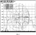
- FIG. 3 is a Smith chart of a printed antenna measured in an embodiment of the present invention, where the Smith chart is a polar coordinate chart of a reflection factor (represented by the symbol ⁇ ), and the reflection factor may be defined as a one-port scattering parameter, that is S11.
- the vertical coordinate is a reflection factor (S11)
- the horizontal coordinate is a frequency.
- Table 1 is antenna efficiency actually measured in this embodiment of the present invention. Efficiency, which is measured based on this embodiment of the present invention, of an antenna at low frequency band and at high frequency band respectively can be seen in Table 1.
- Table 1 Frequency Efficiency (%) Frequency Efficiency (%) Frequency Efficiency (%) 698 67.1 1790 53.2 2170 59.0 711 73.5 1810 57.7 2190 55.5 731 78.4 1830 58.5 2300 60.2 751 76.4 1850 58.7 2350 59.5 771 73.9 1870 59.6 2400 60.3 791 74.0 1890 60.6 2450 59.9 810 66.8 1910 61.2 2500 60.2 830 62.9 1930 61.7 2520 57.7 850 61.1 1950 65.1 2540 58.6 870 58.1 1970 63.5 2560 60.8 890 53.7 1990 61.9 2580 53.9 910 47.6 2010 60.1 2600 53.8 930 46.4 2030 60.1 2620 48.6 950 34.7 2050 57.4 2640 50.3
- measured antenna efficiency at a low frequency band (698 MHz to 950 MHz) is higher than 35%
- measured antenna efficiency at a high frequency band (1.71 GHz to 2.7 GHz) is higher than 45%.
- a printed antenna that can increase a bandwidth is designed.
- a first antenna pattern is connected to a second antenna pattern to form a non-closed rectangular, and a third antenna pattern is arranged in parallel in the non-closed rectangle, and is separately connected to the first antenna pattern and the second antenna pattern.
- the printed antenna can satisfy a requirement of a low frequency bandwidth of LTE communication (as low as 700 MHz), and efficiency of the printed antenna is effectively improved at a full frequency band.
- the printed antenna may implement a coverage of an LTE full frequency band with no or few matching devices, which facilitates integration of the printed antenna in a terminal product, so as to satisfy a requirement of product miniaturization, and effectively reduce costs.
- FIG. 4 is a schematic structural diagram of a printed antenna according to another embodiment of the present invention.
- the printed antenna includes: a printed circuit board 401, an antenna pattern, and a signal feed-in point 402, where the antenna pattern is printed on a front surface of the printed circuit board 401.
- the antenna pattern includes: a first antenna pattern 403, a second antenna pattern 404, a third antenna pattern 405, and a welding element 406.
- the signal feed-in point 402 is connected to the second antenna pattern 404.
- One end of a side, which is laid out along an edge of the printed circuit board 401, of the first antenna pattern 403 is connected to the second antenna pattern 404.
- the second antenna pattern 404 is vertically laid out in parallel to an edge of the printed circuit board 401, where the second antenna pattern 404 and the first antenna pattern 403 form a non-closed rectangular.
- the third antenna pattern 405 includes a first part 4051 and a second part 4052, where one end of the first part 4051 of the third antenna pattern 405 is connected to the first antenna pattern 403, and one end of the second part 4052 of the third antenna pattern 405 is connected to the second antenna pattern 404, and the first part 4051 and the second part 4052 are arranged in parallel in the non-closed rectangle.
- the welding element 406 includes at least one of the following: an inductor, a capacitor, a resistor, or the like.
- One end of the first part 4051 of the third antenna pattern 405 is connected to the first antenna pattern 403 by using the welding element 406, and/or one end of the second part 4052 of the third antenna pattern 405 is connected to the second antenna pattern 404 by using the welding element 406.
- a connection position between the first antenna pattern 403 and the first part 4051 of the third antenna pattern 405 may be adjusted, and a connection position between the second antenna pattern 404 and the second part 4052 of the third antenna pattern 405 may also be adjusted, and a high-frequency resonance point of the printed antenna may be adjusted, so as to selectively increase radiation power of some resonance frequencies.
- a printed antenna that can increase a bandwidth is designed.
- a first antenna pattern is connected to a second antenna pattern to form a non-closed rectangular, and a third antenna pattern is arranged in parallel in the non-closed rectangle, and is separately connected to the first antenna pattern and the second antenna pattern.
- the printed antenna can satisfy a requirement of a low frequency bandwidth of LTE communication (as low as 700 MHz), and efficiency of the printed antenna is effectively improved at a full frequency band.
- the antenna adjusts a length and a position of a first part and a second part of a third antenna pattern by using a welding element, and a high-frequency resonance point may be adjusted, so as to increase power of some frequencies.
- the printed antenna may implement a coverage of an LTE full frequency band with no or few matching devices, which facilities integration of the printed antenna in a terminal product, so as to satisfy a requirement of product miniaturization, and effectively reduce costs.
- FIG. 5 is a schematic structural diagram of a printed antenna according to still another embodiment of the present invention.
- the printed antenna includes a printed circuit board 501, an antenna pattern, and a signal feed-in point 502, where the antenna pattern is printed on a front surface of the printed circuit board 501.
- the antenna pattern includes: a first antenna pattern 503, a second antenna pattern 504, a third antenna pattern 505, and a welding element 506.
- the signal feed-in point 502 is connected to the second antenna pattern 504.
- One end of a side, which is laid out along an edge of the printed circuit board 501, of the first antenna pattern 503 is connected to the second antenna pattern 504.
- the second antenna pattern 504 is vertically laid out in parallel to an edge of the printed circuit board 501, where the second antenna pattern 504 and the first antenna pattern 503 form a non-closed rectangular.
- the third antenna pattern 505 includes a first part 5051 and a second part 5052, where one end of the first part 5051 of the third antenna pattern 505 is connected to the first antenna pattern 503, and one end of the second part 5052 of the third antenna pattern 505 is connected to the second antenna pattern 504, and the first part 5051 and the second part 5052 are arranged in parallel in the non-closed rectangle.
- the welding element 506 includes at least one of the following: an inductor, a capacitor, a resistor, or the like.
- One end of the first part 5051 of the third antenna pattern 505 is connected to the first antenna pattern 503 by using the welding element 506, and/or one end of the second part 5052 of the third antenna pattern 505 is connected to the second antenna pattern 504 by using the welding element 506.
- the first part 5051 of the third antenna pattern 505 includes a first component 50511 and a second component 50512, where the first component 50511 of the first part 5051 of the third antenna pattern 505 may be connected to the second component 50512 of the first part 5051 by using the welding element 506; and/or the second part 5052 of the third antenna pattern 505 includes a first component 50521 and a second component 50522, where the first component 50521 of the second part 5052 of the third antenna pattern 505 may be connected to the second component 50522 of the second part 5052 by using the welding element 506.
- the first part 5051 of the third antenna pattern 505 includes at least two components, where the at least two components are connected by using the welding element 506, so as to adjust a length of the first part 5051 of the third antenna pattern 505.
- the second part 5052 of the third antenna pattern 505 includes at least two components, where the at least two components are connected by using the welding element 506, so as to adjust a length of the second part 5052 of the third antenna pattern 505.
- a high-frequency resonance point of the printed antenna may be adjusted, so as to selectively increase radiation power of some resonance frequencies.
- a printed antenna that can increase a bandwidth.
- Three sides of a first antenna pattern and a second antenna pattern form a non-closed rectangular, and two parts of a third antenna pattern are alternately arranged in parallel, and are separately connected to the first antenna pattern and the second antenna pattern.
- the printed antenna can satisfy a requirement of a low frequency bandwidth of LTE communication (as low as 700 MHz), and efficiency of the printed antenna is effectively improved at a full frequency band.
- the antenna adjusts a position of a pattern, which is alternately arranged in parallel, of the third antenna pattern by using a welding element, and a high-frequency resonance point may be adjusted, so as to increase power of some frequencies.
- the printed antenna may implement a coverage of an LTE full frequency band with no or few matching devices, which facilitates integration of the printed antenna in a terminal product, so as to satisfy a requirement of product miniaturization, and effectively reduce costs.
- FIG. 6 is a schematic structural diagram of a terminal device according to an embodiment of the present invention. As shown in FIG. 6 , the terminal device 60 includes: at least one printed antenna 601 and a communications module 602.
- the printed antenna 601 includes a printed circuit board, an antenna pattern, and a signal feed-in point, where the antenna pattern is printed on a front surface of the printed circuit board, and the antenna pattern includes a first antenna pattern, a second antenna pattern, and a third antenna pattern; the signal feed-in point is connected to the second antenna pattern; one end of a side, which is laid out along an edge of the printed circuit board, of the first antenna pattern is connected to the second antenna pattern; the second antenna pattern is vertically laid out in parallel to an edge of the printed circuit board, where the second antenna pattern and the first antenna form a non-closed rectangular; and the third antenna pattern includes a first part and a second part, where one end of the first part of the third antenna pattern is connected to the first antenna pattern, and one end of the second part of the third antenna pattern is connected to the second antenna pattern, and the first part and the second part are arranged in parallel in the non-closed rectangle.
- the communications module 602 is configured to access a wireless network by using the printed antenna.
- FIG. 7 is a schematic structural diagram of a terminal device according to another embodiment of the present invention.
- the terminal device includes at least two printed antennas, where a first printed antenna 6011 is a primary antenna of the terminal device 60, and a second printed antenna 6012 is a secondary antenna of the terminal device 60; and the second printed antenna 6012 is a diversity antenna of the terminal device 60 and implements diversity reception of a signal together with the first printed antenna.
- the terminal device 60 may include at least one of the following: a data card, a wireless network interface card, a modem, a mobile phone, a portable computer that has a function of surfing the Internet, or a device that can perform wireless communication.
- the printed antenna 601 may also be configured to implement functions such as Bluetooth, WIFI (Wireless Fidelity), GPS (Global Positioning System).
- a printed antenna that can increase a bandwidth is designed.
- a first antenna pattern is connected to a second antenna pattern to form a non-closed rectangular, and a third antenna pattern is arranged in parallel in the non-closed rectangle, and is separately connected to the first antenna pattern and the second antenna pattern.
- the printed antenna can satisfy a requirement of a low frequency bandwidth of LTE communication (as low as 700 MHz), and efficiency of the printed antenna is effectively improved at a full frequency band.
- the antenna adjusts a position of a pattern, which is alternately arranged in parallel, of the third antenna pattern by using a welding element, and a high-frequency resonance point may be adjusted, so as to increase power of some frequencies.
- the printed antenna may implement a coverage of an LTE full frequency band with no or few matching devices, which facilitates integration of the printed antenna in a terminal product, so as to satisfy a requirement of product miniaturization, and effectively reduce costs.
- the disclosed server and method may be implemented in other manners.
- the described server embodiment is merely exemplary.
- the unit division is merely logical function division and may be other division in an actual implementation.
- a plurality of units or components may be combined or integrated into another system, or some features may be ignored or not performed.
- the displayed or discussed mutual couplings or direct couplings or communication connections may be implemented through some interfaces.
- the indirect couplings or communication connections between the apparatuses or units may be implemented in electronic, mechanical, or other forms.
- the units described as separate parts may or may not be physically separate, and parts displayed as units may or may not be physical units, may be located in one position, or may be distributed on a plurality of network units. A part or all of the units may be selected according to actual needs to achieve the objectives of the solutions of the embodiments of the present invention.
- functional units in the embodiments of the present invention may be integrated into one processing unit, or each of the units may exist alone physically, or two or more units are integrated into one unit.
- the program may be stored in a computer readable storage medium. When the program runs, the steps of the method embodiments are performed.
- the foregoing storage medium includes any medium that can store program code, such as a ROM, a RAM, a magnetic disk, or an optical disc.
Applications Claiming Priority (2)
| Application Number | Priority Date | Filing Date | Title |
|---|---|---|---|
| CN201310329288.2A CN104347926B (zh) | 2013-07-31 | 2013-07-31 | 一种印制天线和终端设备 |
| PCT/CN2014/082014 WO2015014200A1 (zh) | 2013-07-31 | 2014-07-11 | 一种印制天线和终端设备 |
Publications (3)
| Publication Number | Publication Date |
|---|---|
| EP2871714A1 EP2871714A1 (en) | 2015-05-13 |
| EP2871714A4 EP2871714A4 (en) | 2015-07-15 |
| EP2871714B1 true EP2871714B1 (en) | 2020-09-09 |
Family
ID=52430969
Family Applications (1)
| Application Number | Title | Priority Date | Filing Date |
|---|---|---|---|
| EP14814654.1A Active EP2871714B1 (en) | 2013-07-31 | 2014-07-11 | Printed antenna and terminal device |
Country Status (5)
| Country | Link |
|---|---|
| US (1) | US9847580B2 (zh) |
| EP (1) | EP2871714B1 (zh) |
| JP (1) | JP5970725B2 (zh) |
| CN (1) | CN104347926B (zh) |
| WO (1) | WO2015014200A1 (zh) |
Families Citing this family (6)
| Publication number | Priority date | Publication date | Assignee | Title |
|---|---|---|---|---|
| CN105990679B (zh) * | 2015-02-13 | 2019-03-05 | 鸿富锦精密工业(深圳)有限公司 | 电子装置 |
| JP6916985B2 (ja) * | 2017-01-25 | 2021-08-11 | 日立金属株式会社 | アンテナ装置 |
| KR102019354B1 (ko) * | 2017-11-03 | 2019-09-09 | 삼성전자주식회사 | 안테나 모듈 |
| CN109409484A (zh) * | 2018-10-19 | 2019-03-01 | 威海北洋光电信息技术股份公司 | 基于rfid的双圈切换层板式天线装置 |
| CN113497346B (zh) * | 2020-04-01 | 2022-08-12 | 海信集团有限公司 | 天线、无线通信模块及终端 |
| CN111857430B (zh) * | 2020-07-22 | 2024-01-30 | 京东方科技集团股份有限公司 | 显示面板和显示装置 |
Family Cites Families (24)
| Publication number | Priority date | Publication date | Assignee | Title |
|---|---|---|---|---|
| US3938161A (en) * | 1974-10-03 | 1976-02-10 | Ball Brothers Research Corporation | Microstrip antenna structure |
| JPH07193417A (ja) * | 1993-12-27 | 1995-07-28 | Central Glass Co Ltd | ガラスアンテナ |
| JP3107150B2 (ja) * | 1997-04-11 | 2000-11-06 | 日本電気株式会社 | 交差指状プリントアンテナ |
| WO2001024316A1 (fr) * | 1999-09-30 | 2001-04-05 | Murata Manufacturing Co., Ltd. | Antenne a montage en surface et dispositif de communication avec antenne a montage en surface |
| JP2003188637A (ja) * | 2001-12-20 | 2003-07-04 | Hitachi Cable Ltd | 平板多重アンテナおよび携帯端末 |
| JP2004236273A (ja) * | 2003-02-03 | 2004-08-19 | Matsushita Electric Ind Co Ltd | アンテナ |
| US7055754B2 (en) * | 2003-11-03 | 2006-06-06 | Avery Dennison Corporation | Self-compensating antennas for substrates having differing dielectric constant values |
| TW200512566A (en) * | 2003-09-19 | 2005-04-01 | Quanta Comp Inc | Concealed antenna used in a notebook |
| WO2005062422A1 (en) * | 2003-12-23 | 2005-07-07 | Macquarie University | Multi-band, broadband, fully-planar antennas |
| WO2008087780A1 (ja) * | 2007-01-19 | 2008-07-24 | Murata Manufacturing Co., Ltd. | アンテナ装置及び無線通信機 |
| CN101345337B (zh) * | 2007-07-11 | 2012-08-01 | 西北工业大学 | 一种新型的x波段双频微带天线 |
| WO2009028251A1 (ja) * | 2007-08-24 | 2009-03-05 | Murata Manufacturing Co., Ltd. | アンテナ装置及び無線通信機 |
| JP5777885B2 (ja) * | 2008-01-08 | 2015-09-09 | エース テクノロジーズ コーポレーション | 多重帯域内蔵型アンテナ |
| GB0805393D0 (en) * | 2008-03-26 | 2008-04-30 | Dockon Ltd | Improvements in and relating to antennas |
| KR100980218B1 (ko) * | 2008-03-31 | 2010-09-06 | 주식회사 에이스테크놀로지 | 다중 대역에 대한 임피던스 매칭을 지원하는 내장형 안테나 |
| CN101320837A (zh) * | 2008-07-17 | 2008-12-10 | 上海联能科技有限公司 | 基于复合左右手传输线的超宽带天线 |
| US7773033B2 (en) * | 2008-09-30 | 2010-08-10 | Raytheon Company | Multilayer metamaterial isolator |
| JP2011061638A (ja) * | 2009-09-11 | 2011-03-24 | Tdk Corp | アンテナ装置 |
| CN102763276B (zh) | 2010-02-16 | 2017-07-21 | 株式会社村田制作所 | 天线及无线通信装置 |
| JP2012019281A (ja) * | 2010-07-06 | 2012-01-26 | Toshiba Corp | アンテナ装置、及び無線装置 |
| CN201741807U (zh) * | 2010-07-12 | 2011-02-09 | 全一电子股份有限公司 | 可接收低频的平面双偶极天线 |
| CN102117966B (zh) * | 2011-03-17 | 2013-12-04 | 华为终端有限公司 | 一种印制天线 |
| CN102956960A (zh) * | 2011-08-16 | 2013-03-06 | 华硕电脑股份有限公司 | 天线模块 |
| CN202712428U (zh) * | 2012-03-01 | 2013-01-30 | 西安电子科技大学 | 一种小型超宽带天线 |
-
2013
- 2013-07-31 CN CN201310329288.2A patent/CN104347926B/zh active Active
-
2014
- 2014-07-11 WO PCT/CN2014/082014 patent/WO2015014200A1/zh active Application Filing
- 2014-07-11 EP EP14814654.1A patent/EP2871714B1/en active Active
- 2014-07-11 JP JP2015528870A patent/JP5970725B2/ja active Active
- 2014-12-22 US US14/579,897 patent/US9847580B2/en active Active
Non-Patent Citations (1)
| Title |
|---|
| None * |
Also Published As
| Publication number | Publication date |
|---|---|
| JP2015530809A (ja) | 2015-10-15 |
| US20150102978A1 (en) | 2015-04-16 |
| EP2871714A4 (en) | 2015-07-15 |
| EP2871714A1 (en) | 2015-05-13 |
| JP5970725B2 (ja) | 2016-08-17 |
| WO2015014200A1 (zh) | 2015-02-05 |
| US9847580B2 (en) | 2017-12-19 |
| CN104347926B (zh) | 2017-04-19 |
| CN104347926A (zh) | 2015-02-11 |
Similar Documents
| Publication | Publication Date | Title |
|---|---|---|
| EP2871714B1 (en) | Printed antenna and terminal device | |
| US10601117B2 (en) | Antenna and mobile terminal | |
| JP6118889B2 (ja) | 移動端末装置 | |
| TWI628867B (zh) | 天線組件及具有該天線組件的無線通訊裝置 | |
| US10218051B2 (en) | Antenna structure and wireless communication device using same | |
| US10177439B2 (en) | Antenna structure and wireless communication device using same | |
| CA2898060C (en) | Mobile wireless communications device with improved broadband antenna impedance matching | |
| JP2016082559A (ja) | アンテナ構造体及びこれを備える無線通信装置 | |
| EP2991363A1 (en) | Wireless communications device | |
| US20220278446A1 (en) | Antenna and electronic device | |
| EP3043418A1 (en) | Terminal having multimode antenna | |
| US10069193B2 (en) | Antenna and mobile terminal | |
| US9450287B2 (en) | Broadband antenna and wireless communication device employing same | |
| US10305169B2 (en) | Antenna apparatus and terminal | |
| CN104092004B (zh) | 天线结构 | |
| TWI571002B (zh) | 天線裝置及應用其之通訊裝置 | |
| EP3261178B1 (en) | Slot antenna | |
| US20140313097A1 (en) | Gps antenna, motherboard employing same, and wireless communication device employing motherboard | |
| CN103427861A (zh) | 通信装置 | |
| US11114746B2 (en) | Terminal | |
| CN105811081A (zh) | 天线结构及具有该天线结构的无线通信装置 |
Legal Events
| Date | Code | Title | Description |
|---|---|---|---|
| PUAI | Public reference made under article 153(3) epc to a published international application that has entered the european phase |
Free format text: ORIGINAL CODE: 0009012 |
|
| 17P | Request for examination filed |
Effective date: 20141229 |
|
| AK | Designated contracting states |
Kind code of ref document: A1 Designated state(s): AL AT BE BG CH CY CZ DE DK EE ES FI FR GB GR HR HU IE IS IT LI LT LU LV MC MK MT NL NO PL PT RO RS SE SI SK SM TR |
|
| AX | Request for extension of the european patent |
Extension state: BA ME |
|
| RA4 | Supplementary search report drawn up and despatched (corrected) |
Effective date: 20150615 |
|
| RIC1 | Information provided on ipc code assigned before grant |
Ipc: H01Q 9/04 20060101ALI20150609BHEP Ipc: H01Q 5/371 20150101ALI20150609BHEP Ipc: H01Q 1/38 20060101AFI20150609BHEP Ipc: H01Q 5/321 20150101ALI20150609BHEP |
|
| DAX | Request for extension of the european patent (deleted) | ||
| RAP1 | Party data changed (applicant data changed or rights of an application transferred) |
Owner name: HUAWEI DEVICE (SHENZHEN) CO., LTD. |
|
| RAP1 | Party data changed (applicant data changed or rights of an application transferred) |
Owner name: HUAWEI DEVICE CO., LTD. |
|
| STAA | Information on the status of an ep patent application or granted ep patent |
Free format text: STATUS: EXAMINATION IS IN PROGRESS |
|
| 17Q | First examination report despatched |
Effective date: 20190624 |
|
| GRAP | Despatch of communication of intention to grant a patent |
Free format text: ORIGINAL CODE: EPIDOSNIGR1 |
|
| STAA | Information on the status of an ep patent application or granted ep patent |
Free format text: STATUS: GRANT OF PATENT IS INTENDED |
|
| INTG | Intention to grant announced |
Effective date: 20200325 |
|
| GRAS | Grant fee paid |
Free format text: ORIGINAL CODE: EPIDOSNIGR3 |
|
| GRAA | (expected) grant |
Free format text: ORIGINAL CODE: 0009210 |
|
| STAA | Information on the status of an ep patent application or granted ep patent |
Free format text: STATUS: THE PATENT HAS BEEN GRANTED |
|
| AK | Designated contracting states |
Kind code of ref document: B1 Designated state(s): AL AT BE BG CH CY CZ DE DK EE ES FI FR GB GR HR HU IE IS IT LI LT LU LV MC MK MT NL NO PL PT RO RS SE SI SK SM TR |
|
| REG | Reference to a national code |
Ref country code: GB Ref legal event code: FG4D |
|
| REG | Reference to a national code |
Ref country code: AT Ref legal event code: REF Ref document number: 1312711 Country of ref document: AT Kind code of ref document: T Effective date: 20200915 Ref country code: CH Ref legal event code: EP |
|
| REG | Reference to a national code |
Ref country code: DE Ref legal event code: R096 Ref document number: 602014070049 Country of ref document: DE |
|
| REG | Reference to a national code |
Ref country code: IE Ref legal event code: FG4D |
|
| REG | Reference to a national code |
Ref country code: NL Ref legal event code: FP |
|
| REG | Reference to a national code |
Ref country code: LT Ref legal event code: MG4D |
|
| PG25 | Lapsed in a contracting state [announced via postgrant information from national office to epo] |
Ref country code: LT Free format text: LAPSE BECAUSE OF FAILURE TO SUBMIT A TRANSLATION OF THE DESCRIPTION OR TO PAY THE FEE WITHIN THE PRESCRIBED TIME-LIMIT Effective date: 20200909 Ref country code: HR Free format text: LAPSE BECAUSE OF FAILURE TO SUBMIT A TRANSLATION OF THE DESCRIPTION OR TO PAY THE FEE WITHIN THE PRESCRIBED TIME-LIMIT Effective date: 20200909 Ref country code: NO Free format text: LAPSE BECAUSE OF FAILURE TO SUBMIT A TRANSLATION OF THE DESCRIPTION OR TO PAY THE FEE WITHIN THE PRESCRIBED TIME-LIMIT Effective date: 20201209 Ref country code: SE Free format text: LAPSE BECAUSE OF FAILURE TO SUBMIT A TRANSLATION OF THE DESCRIPTION OR TO PAY THE FEE WITHIN THE PRESCRIBED TIME-LIMIT Effective date: 20200909 Ref country code: FI Free format text: LAPSE BECAUSE OF FAILURE TO SUBMIT A TRANSLATION OF THE DESCRIPTION OR TO PAY THE FEE WITHIN THE PRESCRIBED TIME-LIMIT Effective date: 20200909 Ref country code: GR Free format text: LAPSE BECAUSE OF FAILURE TO SUBMIT A TRANSLATION OF THE DESCRIPTION OR TO PAY THE FEE WITHIN THE PRESCRIBED TIME-LIMIT Effective date: 20201210 Ref country code: BG Free format text: LAPSE BECAUSE OF FAILURE TO SUBMIT A TRANSLATION OF THE DESCRIPTION OR TO PAY THE FEE WITHIN THE PRESCRIBED TIME-LIMIT Effective date: 20201209 |
|
| REG | Reference to a national code |
Ref country code: AT Ref legal event code: MK05 Ref document number: 1312711 Country of ref document: AT Kind code of ref document: T Effective date: 20200909 |
|
| PG25 | Lapsed in a contracting state [announced via postgrant information from national office to epo] |
Ref country code: PL Free format text: LAPSE BECAUSE OF FAILURE TO SUBMIT A TRANSLATION OF THE DESCRIPTION OR TO PAY THE FEE WITHIN THE PRESCRIBED TIME-LIMIT Effective date: 20200909 Ref country code: LV Free format text: LAPSE BECAUSE OF FAILURE TO SUBMIT A TRANSLATION OF THE DESCRIPTION OR TO PAY THE FEE WITHIN THE PRESCRIBED TIME-LIMIT Effective date: 20200909 Ref country code: RS Free format text: LAPSE BECAUSE OF FAILURE TO SUBMIT A TRANSLATION OF THE DESCRIPTION OR TO PAY THE FEE WITHIN THE PRESCRIBED TIME-LIMIT Effective date: 20200909 |
|
| PG25 | Lapsed in a contracting state [announced via postgrant information from national office to epo] |
Ref country code: CZ Free format text: LAPSE BECAUSE OF FAILURE TO SUBMIT A TRANSLATION OF THE DESCRIPTION OR TO PAY THE FEE WITHIN THE PRESCRIBED TIME-LIMIT Effective date: 20200909 Ref country code: PT Free format text: LAPSE BECAUSE OF FAILURE TO SUBMIT A TRANSLATION OF THE DESCRIPTION OR TO PAY THE FEE WITHIN THE PRESCRIBED TIME-LIMIT Effective date: 20210111 Ref country code: EE Free format text: LAPSE BECAUSE OF FAILURE TO SUBMIT A TRANSLATION OF THE DESCRIPTION OR TO PAY THE FEE WITHIN THE PRESCRIBED TIME-LIMIT Effective date: 20200909 Ref country code: SM Free format text: LAPSE BECAUSE OF FAILURE TO SUBMIT A TRANSLATION OF THE DESCRIPTION OR TO PAY THE FEE WITHIN THE PRESCRIBED TIME-LIMIT Effective date: 20200909 Ref country code: RO Free format text: LAPSE BECAUSE OF FAILURE TO SUBMIT A TRANSLATION OF THE DESCRIPTION OR TO PAY THE FEE WITHIN THE PRESCRIBED TIME-LIMIT Effective date: 20200909 |
|
| PG25 | Lapsed in a contracting state [announced via postgrant information from national office to epo] |
Ref country code: ES Free format text: LAPSE BECAUSE OF FAILURE TO SUBMIT A TRANSLATION OF THE DESCRIPTION OR TO PAY THE FEE WITHIN THE PRESCRIBED TIME-LIMIT Effective date: 20200909 Ref country code: AT Free format text: LAPSE BECAUSE OF FAILURE TO SUBMIT A TRANSLATION OF THE DESCRIPTION OR TO PAY THE FEE WITHIN THE PRESCRIBED TIME-LIMIT Effective date: 20200909 Ref country code: AL Free format text: LAPSE BECAUSE OF FAILURE TO SUBMIT A TRANSLATION OF THE DESCRIPTION OR TO PAY THE FEE WITHIN THE PRESCRIBED TIME-LIMIT Effective date: 20200909 Ref country code: IS Free format text: LAPSE BECAUSE OF FAILURE TO SUBMIT A TRANSLATION OF THE DESCRIPTION OR TO PAY THE FEE WITHIN THE PRESCRIBED TIME-LIMIT Effective date: 20210109 |
|
| REG | Reference to a national code |
Ref country code: DE Ref legal event code: R097 Ref document number: 602014070049 Country of ref document: DE |
|
| PG25 | Lapsed in a contracting state [announced via postgrant information from national office to epo] |
Ref country code: SK Free format text: LAPSE BECAUSE OF FAILURE TO SUBMIT A TRANSLATION OF THE DESCRIPTION OR TO PAY THE FEE WITHIN THE PRESCRIBED TIME-LIMIT Effective date: 20200909 |
|
| PLBE | No opposition filed within time limit |
Free format text: ORIGINAL CODE: 0009261 |
|
| STAA | Information on the status of an ep patent application or granted ep patent |
Free format text: STATUS: NO OPPOSITION FILED WITHIN TIME LIMIT |
|
| 26N | No opposition filed |
Effective date: 20210610 |
|
| PG25 | Lapsed in a contracting state [announced via postgrant information from national office to epo] |
Ref country code: SI Free format text: LAPSE BECAUSE OF FAILURE TO SUBMIT A TRANSLATION OF THE DESCRIPTION OR TO PAY THE FEE WITHIN THE PRESCRIBED TIME-LIMIT Effective date: 20200909 Ref country code: DK Free format text: LAPSE BECAUSE OF FAILURE TO SUBMIT A TRANSLATION OF THE DESCRIPTION OR TO PAY THE FEE WITHIN THE PRESCRIBED TIME-LIMIT Effective date: 20200909 |
|
| PG25 | Lapsed in a contracting state [announced via postgrant information from national office to epo] |
Ref country code: IT Free format text: LAPSE BECAUSE OF FAILURE TO SUBMIT A TRANSLATION OF THE DESCRIPTION OR TO PAY THE FEE WITHIN THE PRESCRIBED TIME-LIMIT Effective date: 20200909 |
|
| REG | Reference to a national code |
Ref country code: CH Ref legal event code: PL |
|
| PG25 | Lapsed in a contracting state [announced via postgrant information from national office to epo] |
Ref country code: MC Free format text: LAPSE BECAUSE OF FAILURE TO SUBMIT A TRANSLATION OF THE DESCRIPTION OR TO PAY THE FEE WITHIN THE PRESCRIBED TIME-LIMIT Effective date: 20200909 |
|
| REG | Reference to a national code |
Ref country code: BE Ref legal event code: MM Effective date: 20210731 |
|
| PG25 | Lapsed in a contracting state [announced via postgrant information from national office to epo] |
Ref country code: LI Free format text: LAPSE BECAUSE OF NON-PAYMENT OF DUE FEES Effective date: 20210731 Ref country code: CH Free format text: LAPSE BECAUSE OF NON-PAYMENT OF DUE FEES Effective date: 20210731 |
|
| PG25 | Lapsed in a contracting state [announced via postgrant information from national office to epo] |
Ref country code: LU Free format text: LAPSE BECAUSE OF NON-PAYMENT OF DUE FEES Effective date: 20210711 |
|
| PG25 | Lapsed in a contracting state [announced via postgrant information from national office to epo] |
Ref country code: IE Free format text: LAPSE BECAUSE OF NON-PAYMENT OF DUE FEES Effective date: 20210711 Ref country code: BE Free format text: LAPSE BECAUSE OF NON-PAYMENT OF DUE FEES Effective date: 20210731 |
|
| PG25 | Lapsed in a contracting state [announced via postgrant information from national office to epo] |
Ref country code: HU Free format text: LAPSE BECAUSE OF FAILURE TO SUBMIT A TRANSLATION OF THE DESCRIPTION OR TO PAY THE FEE WITHIN THE PRESCRIBED TIME-LIMIT; INVALID AB INITIO Effective date: 20140711 |
|
| PG25 | Lapsed in a contracting state [announced via postgrant information from national office to epo] |
Ref country code: CY Free format text: LAPSE BECAUSE OF FAILURE TO SUBMIT A TRANSLATION OF THE DESCRIPTION OR TO PAY THE FEE WITHIN THE PRESCRIBED TIME-LIMIT Effective date: 20200909 |
|
| PGFP | Annual fee paid to national office [announced via postgrant information from national office to epo] |
Ref country code: NL Payment date: 20230614 Year of fee payment: 10 Ref country code: FR Payment date: 20230620 Year of fee payment: 10 |
|
| PGFP | Annual fee paid to national office [announced via postgrant information from national office to epo] |
Ref country code: GB Payment date: 20230601 Year of fee payment: 10 |
|
| PGFP | Annual fee paid to national office [announced via postgrant information from national office to epo] |
Ref country code: DE Payment date: 20230531 Year of fee payment: 10 |
|
| PG25 | Lapsed in a contracting state [announced via postgrant information from national office to epo] |
Ref country code: MK Free format text: LAPSE BECAUSE OF FAILURE TO SUBMIT A TRANSLATION OF THE DESCRIPTION OR TO PAY THE FEE WITHIN THE PRESCRIBED TIME-LIMIT Effective date: 20200909 |