EP2870632B1 - Dispositifs diodes radiales esaki à nanofil et procédés associés - Google Patents
Dispositifs diodes radiales esaki à nanofil et procédés associés Download PDFInfo
- Publication number
- EP2870632B1 EP2870632B1 EP13813238.6A EP13813238A EP2870632B1 EP 2870632 B1 EP2870632 B1 EP 2870632B1 EP 13813238 A EP13813238 A EP 13813238A EP 2870632 B1 EP2870632 B1 EP 2870632B1
- Authority
- EP
- European Patent Office
- Prior art keywords
- core
- shell
- nanowire
- semiconductor
- junction
- Prior art date
- Legal status (The legal status is an assumption and is not a legal conclusion. Google has not performed a legal analysis and makes no representation as to the accuracy of the status listed.)
- Not-in-force
Links
- 239000002070 nanowire Substances 0.000 title claims description 123
- 238000000034 method Methods 0.000 title claims description 15
- 239000004065 semiconductor Substances 0.000 claims description 78
- 230000005641 tunneling Effects 0.000 claims description 48
- 239000000463 material Substances 0.000 claims description 32
- 239000000969 carrier Substances 0.000 claims description 23
- 239000000758 substrate Substances 0.000 claims description 20
- 230000004888 barrier function Effects 0.000 claims description 19
- 230000005684 electric field Effects 0.000 claims description 16
- 230000005669 field effect Effects 0.000 claims description 10
- 239000012777 electrically insulating material Substances 0.000 claims description 6
- 230000008859 change Effects 0.000 claims description 2
- 239000011162 core material Substances 0.000 claims 18
- 239000011257 shell material Substances 0.000 claims 16
- 239000010410 layer Substances 0.000 description 55
- 210000004027 cell Anatomy 0.000 description 25
- 229910000673 Indium arsenide Inorganic materials 0.000 description 18
- RPQDHPTXJYYUPQ-UHFFFAOYSA-N indium arsenide Chemical compound [In]#[As] RPQDHPTXJYYUPQ-UHFFFAOYSA-N 0.000 description 17
- 229910005542 GaSb Inorganic materials 0.000 description 14
- 238000004088 simulation Methods 0.000 description 9
- 230000000873 masking effect Effects 0.000 description 8
- 230000008901 benefit Effects 0.000 description 6
- VYPSYNLAJGMNEJ-UHFFFAOYSA-N Silicium dioxide Chemical compound O=[Si]=O VYPSYNLAJGMNEJ-UHFFFAOYSA-N 0.000 description 4
- 230000015572 biosynthetic process Effects 0.000 description 4
- 230000000694 effects Effects 0.000 description 4
- 229910052751 metal Inorganic materials 0.000 description 4
- 239000002184 metal Substances 0.000 description 4
- 239000002086 nanomaterial Substances 0.000 description 4
- 230000008569 process Effects 0.000 description 4
- 229910001218 Gallium arsenide Inorganic materials 0.000 description 3
- 229910000530 Gallium indium arsenide Inorganic materials 0.000 description 3
- 230000000903 blocking effect Effects 0.000 description 3
- 239000003054 catalyst Substances 0.000 description 3
- 150000001875 compounds Chemical class 0.000 description 3
- 239000002245 particle Substances 0.000 description 3
- 230000005855 radiation Effects 0.000 description 3
- 229910052710 silicon Inorganic materials 0.000 description 3
- 239000010703 silicon Substances 0.000 description 3
- 229910052581 Si3N4 Inorganic materials 0.000 description 2
- XLOMVQKBTHCTTD-UHFFFAOYSA-N Zinc monoxide Chemical compound [Zn]=O XLOMVQKBTHCTTD-UHFFFAOYSA-N 0.000 description 2
- 229910052782 aluminium Inorganic materials 0.000 description 2
- 239000011248 coating agent Substances 0.000 description 2
- 238000000576 coating method Methods 0.000 description 2
- 230000001419 dependent effect Effects 0.000 description 2
- 238000000609 electron-beam lithography Methods 0.000 description 2
- 230000005284 excitation Effects 0.000 description 2
- 239000011229 interlayer Substances 0.000 description 2
- 238000004519 manufacturing process Methods 0.000 description 2
- 230000007246 mechanism Effects 0.000 description 2
- 239000000203 mixture Substances 0.000 description 2
- 238000001020 plasma etching Methods 0.000 description 2
- HQVNEWCFYHHQES-UHFFFAOYSA-N silicon nitride Chemical compound N12[Si]34N5[Si]62N3[Si]51N64 HQVNEWCFYHHQES-UHFFFAOYSA-N 0.000 description 2
- 229910004613 CdTe Inorganic materials 0.000 description 1
- 208000012868 Overgrowth Diseases 0.000 description 1
- 229910004205 SiNX Inorganic materials 0.000 description 1
- 229910000577 Silicon-germanium Inorganic materials 0.000 description 1
- 229910045601 alloy Inorganic materials 0.000 description 1
- 239000000956 alloy Substances 0.000 description 1
- 238000000231 atomic layer deposition Methods 0.000 description 1
- 239000000919 ceramic Substances 0.000 description 1
- 239000002800 charge carrier Substances 0.000 description 1
- 238000004871 chemical beam epitaxy Methods 0.000 description 1
- 229910052681 coesite Inorganic materials 0.000 description 1
- 230000000052 comparative effect Effects 0.000 description 1
- -1 conductive (e.g. Substances 0.000 description 1
- 239000004020 conductor Substances 0.000 description 1
- 229910052802 copper Inorganic materials 0.000 description 1
- 229910052906 cristobalite Inorganic materials 0.000 description 1
- 230000007547 defect Effects 0.000 description 1
- 238000010586 diagram Methods 0.000 description 1
- 239000003989 dielectric material Substances 0.000 description 1
- 238000005530 etching Methods 0.000 description 1
- 229910052732 germanium Inorganic materials 0.000 description 1
- GNPVGFCGXDBREM-UHFFFAOYSA-N germanium atom Chemical compound [Ge] GNPVGFCGXDBREM-UHFFFAOYSA-N 0.000 description 1
- 239000011521 glass Substances 0.000 description 1
- 229910000449 hafnium oxide Inorganic materials 0.000 description 1
- WIHZLLGSGQNAGK-UHFFFAOYSA-N hafnium(4+);oxygen(2-) Chemical compound [O-2].[O-2].[Hf+4] WIHZLLGSGQNAGK-UHFFFAOYSA-N 0.000 description 1
- 125000005842 heteroatom Chemical group 0.000 description 1
- 230000036039 immunity Effects 0.000 description 1
- 239000012535 impurity Substances 0.000 description 1
- AMGQUBHHOARCQH-UHFFFAOYSA-N indium;oxotin Chemical compound [In].[Sn]=O AMGQUBHHOARCQH-UHFFFAOYSA-N 0.000 description 1
- 230000010354 integration Effects 0.000 description 1
- 210000004692 intercellular junction Anatomy 0.000 description 1
- 230000004048 modification Effects 0.000 description 1
- 238000012986 modification Methods 0.000 description 1
- 238000001127 nanoimprint lithography Methods 0.000 description 1
- 239000002073 nanorod Substances 0.000 description 1
- 239000002071 nanotube Substances 0.000 description 1
- TWNQGVIAIRXVLR-UHFFFAOYSA-N oxo(oxoalumanyloxy)alumane Chemical compound O=[Al]O[Al]=O TWNQGVIAIRXVLR-UHFFFAOYSA-N 0.000 description 1
- BPUBBGLMJRNUCC-UHFFFAOYSA-N oxygen(2-);tantalum(5+) Chemical compound [O-2].[O-2].[O-2].[O-2].[O-2].[Ta+5].[Ta+5] BPUBBGLMJRNUCC-UHFFFAOYSA-N 0.000 description 1
- 238000000206 photolithography Methods 0.000 description 1
- 239000004033 plastic Substances 0.000 description 1
- 238000013139 quantization Methods 0.000 description 1
- 239000010453 quartz Substances 0.000 description 1
- 238000000926 separation method Methods 0.000 description 1
- 239000000377 silicon dioxide Substances 0.000 description 1
- 229910052814 silicon oxide Inorganic materials 0.000 description 1
- 229910052709 silver Inorganic materials 0.000 description 1
- 239000007787 solid Substances 0.000 description 1
- 229910052682 stishovite Inorganic materials 0.000 description 1
- 239000002344 surface layer Substances 0.000 description 1
- 229910001936 tantalum oxide Inorganic materials 0.000 description 1
- 229910052719 titanium Inorganic materials 0.000 description 1
- 229910052905 tridymite Inorganic materials 0.000 description 1
- 238000000927 vapour-phase epitaxy Methods 0.000 description 1
- 238000003631 wet chemical etching Methods 0.000 description 1
- 239000011787 zinc oxide Substances 0.000 description 1
Images


Classifications
-
- H—ELECTRICITY
- H01—ELECTRIC ELEMENTS
- H01L—SEMICONDUCTOR DEVICES NOT COVERED BY CLASS H10
- H01L27/00—Devices consisting of a plurality of semiconductor or other solid-state components formed in or on a common substrate
- H01L27/02—Devices consisting of a plurality of semiconductor or other solid-state components formed in or on a common substrate including semiconductor components specially adapted for rectifying, oscillating, amplifying or switching and having potential barriers; including integrated passive circuit elements having potential barriers
- H01L27/04—Devices consisting of a plurality of semiconductor or other solid-state components formed in or on a common substrate including semiconductor components specially adapted for rectifying, oscillating, amplifying or switching and having potential barriers; including integrated passive circuit elements having potential barriers the substrate being a semiconductor body
- H01L27/06—Devices consisting of a plurality of semiconductor or other solid-state components formed in or on a common substrate including semiconductor components specially adapted for rectifying, oscillating, amplifying or switching and having potential barriers; including integrated passive circuit elements having potential barriers the substrate being a semiconductor body including a plurality of individual components in a non-repetitive configuration
- H01L27/0611—Devices consisting of a plurality of semiconductor or other solid-state components formed in or on a common substrate including semiconductor components specially adapted for rectifying, oscillating, amplifying or switching and having potential barriers; including integrated passive circuit elements having potential barriers the substrate being a semiconductor body including a plurality of individual components in a non-repetitive configuration integrated circuits having a two-dimensional layout of components without a common active region
- H01L27/0617—Devices consisting of a plurality of semiconductor or other solid-state components formed in or on a common substrate including semiconductor components specially adapted for rectifying, oscillating, amplifying or switching and having potential barriers; including integrated passive circuit elements having potential barriers the substrate being a semiconductor body including a plurality of individual components in a non-repetitive configuration integrated circuits having a two-dimensional layout of components without a common active region comprising components of the field-effect type
- H01L27/0629—Devices consisting of a plurality of semiconductor or other solid-state components formed in or on a common substrate including semiconductor components specially adapted for rectifying, oscillating, amplifying or switching and having potential barriers; including integrated passive circuit elements having potential barriers the substrate being a semiconductor body including a plurality of individual components in a non-repetitive configuration integrated circuits having a two-dimensional layout of components without a common active region comprising components of the field-effect type in combination with diodes, or resistors, or capacitors
-
- B—PERFORMING OPERATIONS; TRANSPORTING
- B82—NANOTECHNOLOGY
- B82Y—SPECIFIC USES OR APPLICATIONS OF NANOSTRUCTURES; MEASUREMENT OR ANALYSIS OF NANOSTRUCTURES; MANUFACTURE OR TREATMENT OF NANOSTRUCTURES
- B82Y10/00—Nanotechnology for information processing, storage or transmission, e.g. quantum computing or single electron logic
-
- H—ELECTRICITY
- H01—ELECTRIC ELEMENTS
- H01L—SEMICONDUCTOR DEVICES NOT COVERED BY CLASS H10
- H01L29/00—Semiconductor devices specially adapted for rectifying, amplifying, oscillating or switching and having potential barriers; Capacitors or resistors having potential barriers, e.g. a PN-junction depletion layer or carrier concentration layer; Details of semiconductor bodies or of electrodes thereof ; Multistep manufacturing processes therefor
- H01L29/02—Semiconductor bodies ; Multistep manufacturing processes therefor
- H01L29/06—Semiconductor bodies ; Multistep manufacturing processes therefor characterised by their shape; characterised by the shapes, relative sizes, or dispositions of the semiconductor regions ; characterised by the concentration or distribution of impurities within semiconductor regions
- H01L29/0657—Semiconductor bodies ; Multistep manufacturing processes therefor characterised by their shape; characterised by the shapes, relative sizes, or dispositions of the semiconductor regions ; characterised by the concentration or distribution of impurities within semiconductor regions characterised by the shape of the body
- H01L29/0665—Semiconductor bodies ; Multistep manufacturing processes therefor characterised by their shape; characterised by the shapes, relative sizes, or dispositions of the semiconductor regions ; characterised by the concentration or distribution of impurities within semiconductor regions characterised by the shape of the body the shape of the body defining a nanostructure
- H01L29/0669—Nanowires or nanotubes
- H01L29/0676—Nanowires or nanotubes oriented perpendicular or at an angle to a substrate
-
- H—ELECTRICITY
- H01—ELECTRIC ELEMENTS
- H01L—SEMICONDUCTOR DEVICES NOT COVERED BY CLASS H10
- H01L29/00—Semiconductor devices specially adapted for rectifying, amplifying, oscillating or switching and having potential barriers; Capacitors or resistors having potential barriers, e.g. a PN-junction depletion layer or carrier concentration layer; Details of semiconductor bodies or of electrodes thereof ; Multistep manufacturing processes therefor
- H01L29/02—Semiconductor bodies ; Multistep manufacturing processes therefor
- H01L29/06—Semiconductor bodies ; Multistep manufacturing processes therefor characterised by their shape; characterised by the shapes, relative sizes, or dispositions of the semiconductor regions ; characterised by the concentration or distribution of impurities within semiconductor regions
- H01L29/0657—Semiconductor bodies ; Multistep manufacturing processes therefor characterised by their shape; characterised by the shapes, relative sizes, or dispositions of the semiconductor regions ; characterised by the concentration or distribution of impurities within semiconductor regions characterised by the shape of the body
- H01L29/0665—Semiconductor bodies ; Multistep manufacturing processes therefor characterised by their shape; characterised by the shapes, relative sizes, or dispositions of the semiconductor regions ; characterised by the concentration or distribution of impurities within semiconductor regions characterised by the shape of the body the shape of the body defining a nanostructure
- H01L29/0669—Nanowires or nanotubes
- H01L29/068—Nanowires or nanotubes comprising a junction
-
- H—ELECTRICITY
- H01—ELECTRIC ELEMENTS
- H01L—SEMICONDUCTOR DEVICES NOT COVERED BY CLASS H10
- H01L29/00—Semiconductor devices specially adapted for rectifying, amplifying, oscillating or switching and having potential barriers; Capacitors or resistors having potential barriers, e.g. a PN-junction depletion layer or carrier concentration layer; Details of semiconductor bodies or of electrodes thereof ; Multistep manufacturing processes therefor
- H01L29/02—Semiconductor bodies ; Multistep manufacturing processes therefor
- H01L29/12—Semiconductor bodies ; Multistep manufacturing processes therefor characterised by the materials of which they are formed
- H01L29/122—Single quantum well structures
-
- H—ELECTRICITY
- H01—ELECTRIC ELEMENTS
- H01L—SEMICONDUCTOR DEVICES NOT COVERED BY CLASS H10
- H01L29/00—Semiconductor devices specially adapted for rectifying, amplifying, oscillating or switching and having potential barriers; Capacitors or resistors having potential barriers, e.g. a PN-junction depletion layer or carrier concentration layer; Details of semiconductor bodies or of electrodes thereof ; Multistep manufacturing processes therefor
- H01L29/02—Semiconductor bodies ; Multistep manufacturing processes therefor
- H01L29/12—Semiconductor bodies ; Multistep manufacturing processes therefor characterised by the materials of which they are formed
- H01L29/20—Semiconductor bodies ; Multistep manufacturing processes therefor characterised by the materials of which they are formed including, apart from doping materials or other impurities, only AIIIBV compounds
- H01L29/201—Semiconductor bodies ; Multistep manufacturing processes therefor characterised by the materials of which they are formed including, apart from doping materials or other impurities, only AIIIBV compounds including two or more compounds, e.g. alloys
- H01L29/205—Semiconductor bodies ; Multistep manufacturing processes therefor characterised by the materials of which they are formed including, apart from doping materials or other impurities, only AIIIBV compounds including two or more compounds, e.g. alloys in different semiconductor regions, e.g. heterojunctions
-
- H—ELECTRICITY
- H01—ELECTRIC ELEMENTS
- H01L—SEMICONDUCTOR DEVICES NOT COVERED BY CLASS H10
- H01L29/00—Semiconductor devices specially adapted for rectifying, amplifying, oscillating or switching and having potential barriers; Capacitors or resistors having potential barriers, e.g. a PN-junction depletion layer or carrier concentration layer; Details of semiconductor bodies or of electrodes thereof ; Multistep manufacturing processes therefor
- H01L29/66—Types of semiconductor device ; Multistep manufacturing processes therefor
- H01L29/66977—Quantum effect devices, e.g. using quantum reflection, diffraction or interference effects, i.e. Bragg- or Aharonov-Bohm effects
-
- H—ELECTRICITY
- H01—ELECTRIC ELEMENTS
- H01L—SEMICONDUCTOR DEVICES NOT COVERED BY CLASS H10
- H01L29/00—Semiconductor devices specially adapted for rectifying, amplifying, oscillating or switching and having potential barriers; Capacitors or resistors having potential barriers, e.g. a PN-junction depletion layer or carrier concentration layer; Details of semiconductor bodies or of electrodes thereof ; Multistep manufacturing processes therefor
- H01L29/66—Types of semiconductor device ; Multistep manufacturing processes therefor
- H01L29/68—Types of semiconductor device ; Multistep manufacturing processes therefor controllable by only the electric current supplied, or only the electric potential applied, to an electrode which does not carry the current to be rectified, amplified or switched
- H01L29/70—Bipolar devices
- H01L29/72—Transistor-type devices, i.e. able to continuously respond to applied control signals
- H01L29/739—Transistor-type devices, i.e. able to continuously respond to applied control signals controlled by field-effect, e.g. bipolar static induction transistors [BSIT]
- H01L29/7391—Gated diode structures
-
- H—ELECTRICITY
- H01—ELECTRIC ELEMENTS
- H01L—SEMICONDUCTOR DEVICES NOT COVERED BY CLASS H10
- H01L29/00—Semiconductor devices specially adapted for rectifying, amplifying, oscillating or switching and having potential barriers; Capacitors or resistors having potential barriers, e.g. a PN-junction depletion layer or carrier concentration layer; Details of semiconductor bodies or of electrodes thereof ; Multistep manufacturing processes therefor
- H01L29/66—Types of semiconductor device ; Multistep manufacturing processes therefor
- H01L29/68—Types of semiconductor device ; Multistep manufacturing processes therefor controllable by only the electric current supplied, or only the electric potential applied, to an electrode which does not carry the current to be rectified, amplified or switched
- H01L29/76—Unipolar devices, e.g. field effect transistors
- H01L29/772—Field effect transistors
- H01L29/78—Field effect transistors with field effect produced by an insulated gate
- H01L29/786—Thin film transistors, i.e. transistors with a channel being at least partly a thin film
- H01L29/78642—Vertical transistors
-
- H—ELECTRICITY
- H01—ELECTRIC ELEMENTS
- H01L—SEMICONDUCTOR DEVICES NOT COVERED BY CLASS H10
- H01L29/00—Semiconductor devices specially adapted for rectifying, amplifying, oscillating or switching and having potential barriers; Capacitors or resistors having potential barriers, e.g. a PN-junction depletion layer or carrier concentration layer; Details of semiconductor bodies or of electrodes thereof ; Multistep manufacturing processes therefor
- H01L29/66—Types of semiconductor device ; Multistep manufacturing processes therefor
- H01L29/86—Types of semiconductor device ; Multistep manufacturing processes therefor controllable only by variation of the electric current supplied, or only the electric potential applied, to one or more of the electrodes carrying the current to be rectified, amplified, oscillated or switched
- H01L29/861—Diodes
- H01L29/88—Tunnel-effect diodes
- H01L29/885—Esaki diodes
-
- H—ELECTRICITY
- H01—ELECTRIC ELEMENTS
- H01L—SEMICONDUCTOR DEVICES NOT COVERED BY CLASS H10
- H01L31/00—Semiconductor devices sensitive to infrared radiation, light, electromagnetic radiation of shorter wavelength or corpuscular radiation and specially adapted either for the conversion of the energy of such radiation into electrical energy or for the control of electrical energy by such radiation; Processes or apparatus specially adapted for the manufacture or treatment thereof or of parts thereof; Details thereof
- H01L31/0248—Semiconductor devices sensitive to infrared radiation, light, electromagnetic radiation of shorter wavelength or corpuscular radiation and specially adapted either for the conversion of the energy of such radiation into electrical energy or for the control of electrical energy by such radiation; Processes or apparatus specially adapted for the manufacture or treatment thereof or of parts thereof; Details thereof characterised by their semiconductor bodies
- H01L31/0352—Semiconductor devices sensitive to infrared radiation, light, electromagnetic radiation of shorter wavelength or corpuscular radiation and specially adapted either for the conversion of the energy of such radiation into electrical energy or for the control of electrical energy by such radiation; Processes or apparatus specially adapted for the manufacture or treatment thereof or of parts thereof; Details thereof characterised by their semiconductor bodies characterised by their shape or by the shapes, relative sizes or disposition of the semiconductor regions
- H01L31/035209—Semiconductor devices sensitive to infrared radiation, light, electromagnetic radiation of shorter wavelength or corpuscular radiation and specially adapted either for the conversion of the energy of such radiation into electrical energy or for the control of electrical energy by such radiation; Processes or apparatus specially adapted for the manufacture or treatment thereof or of parts thereof; Details thereof characterised by their semiconductor bodies characterised by their shape or by the shapes, relative sizes or disposition of the semiconductor regions comprising a quantum structures
- H01L31/035227—Semiconductor devices sensitive to infrared radiation, light, electromagnetic radiation of shorter wavelength or corpuscular radiation and specially adapted either for the conversion of the energy of such radiation into electrical energy or for the control of electrical energy by such radiation; Processes or apparatus specially adapted for the manufacture or treatment thereof or of parts thereof; Details thereof characterised by their semiconductor bodies characterised by their shape or by the shapes, relative sizes or disposition of the semiconductor regions comprising a quantum structures the quantum structure being quantum wires, or nanorods
-
- H—ELECTRICITY
- H01—ELECTRIC ELEMENTS
- H01L—SEMICONDUCTOR DEVICES NOT COVERED BY CLASS H10
- H01L31/00—Semiconductor devices sensitive to infrared radiation, light, electromagnetic radiation of shorter wavelength or corpuscular radiation and specially adapted either for the conversion of the energy of such radiation into electrical energy or for the control of electrical energy by such radiation; Processes or apparatus specially adapted for the manufacture or treatment thereof or of parts thereof; Details thereof
- H01L31/04—Semiconductor devices sensitive to infrared radiation, light, electromagnetic radiation of shorter wavelength or corpuscular radiation and specially adapted either for the conversion of the energy of such radiation into electrical energy or for the control of electrical energy by such radiation; Processes or apparatus specially adapted for the manufacture or treatment thereof or of parts thereof; Details thereof adapted as photovoltaic [PV] conversion devices
- H01L31/06—Semiconductor devices sensitive to infrared radiation, light, electromagnetic radiation of shorter wavelength or corpuscular radiation and specially adapted either for the conversion of the energy of such radiation into electrical energy or for the control of electrical energy by such radiation; Processes or apparatus specially adapted for the manufacture or treatment thereof or of parts thereof; Details thereof adapted as photovoltaic [PV] conversion devices characterised by potential barriers
- H01L31/068—Semiconductor devices sensitive to infrared radiation, light, electromagnetic radiation of shorter wavelength or corpuscular radiation and specially adapted either for the conversion of the energy of such radiation into electrical energy or for the control of electrical energy by such radiation; Processes or apparatus specially adapted for the manufacture or treatment thereof or of parts thereof; Details thereof adapted as photovoltaic [PV] conversion devices characterised by potential barriers the potential barriers being only of the PN homojunction type, e.g. bulk silicon PN homojunction solar cells or thin film polycrystalline silicon PN homojunction solar cells
- H01L31/0687—Multiple junction or tandem solar cells
-
- H—ELECTRICITY
- H01—ELECTRIC ELEMENTS
- H01L—SEMICONDUCTOR DEVICES NOT COVERED BY CLASS H10
- H01L29/00—Semiconductor devices specially adapted for rectifying, amplifying, oscillating or switching and having potential barriers; Capacitors or resistors having potential barriers, e.g. a PN-junction depletion layer or carrier concentration layer; Details of semiconductor bodies or of electrodes thereof ; Multistep manufacturing processes therefor
- H01L29/40—Electrodes ; Multistep manufacturing processes therefor
- H01L29/43—Electrodes ; Multistep manufacturing processes therefor characterised by the materials of which they are formed
- H01L29/49—Metal-insulator-semiconductor electrodes, e.g. gates of MOSFET
- H01L29/51—Insulating materials associated therewith
- H01L29/517—Insulating materials associated therewith the insulating material comprising a metallic compound, e.g. metal oxide, metal silicate
-
- Y—GENERAL TAGGING OF NEW TECHNOLOGICAL DEVELOPMENTS; GENERAL TAGGING OF CROSS-SECTIONAL TECHNOLOGIES SPANNING OVER SEVERAL SECTIONS OF THE IPC; TECHNICAL SUBJECTS COVERED BY FORMER USPC CROSS-REFERENCE ART COLLECTIONS [XRACs] AND DIGESTS
- Y02—TECHNOLOGIES OR APPLICATIONS FOR MITIGATION OR ADAPTATION AGAINST CLIMATE CHANGE
- Y02E—REDUCTION OF GREENHOUSE GAS [GHG] EMISSIONS, RELATED TO ENERGY GENERATION, TRANSMISSION OR DISTRIBUTION
- Y02E10/00—Energy generation through renewable energy sources
- Y02E10/50—Photovoltaic [PV] energy
- Y02E10/544—Solar cells from Group III-V materials
-
- Y—GENERAL TAGGING OF NEW TECHNOLOGICAL DEVELOPMENTS; GENERAL TAGGING OF CROSS-SECTIONAL TECHNOLOGIES SPANNING OVER SEVERAL SECTIONS OF THE IPC; TECHNICAL SUBJECTS COVERED BY FORMER USPC CROSS-REFERENCE ART COLLECTIONS [XRACs] AND DIGESTS
- Y02—TECHNOLOGIES OR APPLICATIONS FOR MITIGATION OR ADAPTATION AGAINST CLIMATE CHANGE
- Y02E—REDUCTION OF GREENHOUSE GAS [GHG] EMISSIONS, RELATED TO ENERGY GENERATION, TRANSMISSION OR DISTRIBUTION
- Y02E10/00—Energy generation through renewable energy sources
- Y02E10/50—Photovoltaic [PV] energy
- Y02E10/547—Monocrystalline silicon PV cells
Definitions
- Tunnel or tunneling field effect transistors in the form of gated Esaki diodes (e.g., gated diodes having a negative resistance characteristics and/or operating in the reverse or Zener direction) are currently considered for digital applications operating at V DD ⁇ 0.3V.
- the main merit of these transistors is the possibility to reduce the off current at reduced gate swing using the steep slope where the transistors operate below the thermal limit of kT/q.
- the transistor operation relies on a band pass effect where the drive current is obtained based on tunneling across the bandgap (e.g., electrons tunneling from the conduction band of the n-type semiconductor material into a valence band of an adjacent p-type semiconductor material of a pn junction) that is controlled via the transistor gate.
- the off-current is reduced by the limited number of available states as the band gap is blocking direct tunneling of the carriers.
- the main figures of merit for the tunnel transistor include the drive current, that is the current-level in the on-state, inverse sub-threshold slope (or sub-threshold swing) as well as the off-state current that defines how accurately the transistor may be turned off.
- the off-state is generally not an issue for a TFET since the off-state current is dictated by the reverse leakage current of the pn junction.
- Part of the problem is related to the requirement of accurate alignment of the gate electrode with the pn-junction, where misalignment will reduce the gate effect and lower the electric field across the junction.
- the Esaki diodes preferably are fabricated in materials with small effective mass to increase the tunneling current and that heterostructures preferably are used to increase the drive current, one example being InAs/GaSb. Further problems are the effect of the D it that will increase the slope and in particular for hetero structure devices it is challenging to identify and to process high- ⁇ dielectrics which are compatible with different semiconductor materials.
- WO2008079077 provides a semiconductor device comprising a semiconductor nanoelement (100) and a volume element (105) arranged in epitaxial connection to each other.
- the semiconductor device is electrically connectable with the volume element (105) and the nanoelement (100) electrically connected in series.
- the volume element (105) is at least partly doped to provide a high charge carrier concentration into the nanoelement (100) and a low access resistance in an electrical connection to the volume element (105).
- WO2011049529 discloses a tunnel diode and a method for manufacturing thereof.
- the tunnel diode comprises a p-doped semiconductor region and an n-doped semiconductor region forming a pn-junction at least partly within a nanowire.
- the nanowire is made of one or more compound semiconductor materials forming a homojunction or a heterojunction tunnel diode.
- EP1892769 is directed to photovoltaic devices (e.g., solar cells) comprising elongated nanostructures coated with a thin conformal coating.
- a conformal coating provides a substantially continuous charge separating junction.
- Such devices can comprise a p-n junction, a p-i-n junction (with a thin intrinsic tunneling layer in between the p and n layers), and/or a heterojunction.
- the elongated nanostructures are active photovoltaic (PV) elements in the photovoltaic device.
- EP2472585 discloses a tunnel field effect transistor which is capable of operating at a low subthreshold and is able to be manufactured easily.
- the tunnel field effect transistor includes a group IV semiconductor substrate having a (111) surface and doped so as to have a first conductivity type, a group III-V compound semiconductor nanowire arranged on the (111) surface and containing a first region connected to the (111) surface and a second region doped so as to have a second conductivity type, a source electrode connected to the group IV semiconductor substrate; a drain electrode connected to the second region, and a gate electrode for applying an electric field to an interface between the (111) surface and the group III-V compound semiconductor nanowire, or an interface between the first region and the second region.
- the invention concerns a device comprising a gated tunnel field effect transistor according to claim 1, as well as a method of operating such a device according to claim 8.
- a device comprises a radial nanowire Esaki diode, where the radial nanowire comprises a semiconductor core of a first conductivity type and a semiconductor shell of a second conductivity type different from the first conductivity type.
- the device comprises a gated Esaki diode (e.g., TFET) which includes a radial semiconductor nanowire.
- TFET gated Esaki diode
- the tunneling current between oppositely doped core and shell of the radial semiconductor nanowire flows substantially parallel to an electrical field provided by a gate electrode to the radial semiconductor nanowire.
- the device comprises a multi-junction solar cell which includes a planar solar cell and the radial nanowire Esaki diode.
- nanowires are to be interpreted as having nanometer dimensions in their width and diameter and typically having an elongated shape.
- Such structures are commonly also referred to as nanowhiskers, nanorods, nanotubes, one-dimensional nanoelements, etc.
- the nanowire is an essentially rod-shaped semiconductor structure with a diameter less than 1 micron, such as 500 nm or less and a length up to several microns.
- the nanowire is at its base connected to a substrate, which may include epitaxial semiconductor layers below the nanowire.
- nanowires may be grown without the use of a particle as a catalyst.
- the nanowire protrudes through an opening in a growth mask, such as a mask made of silicon nitride or another insulating layer.
- the nanowire is grown by first providing a growth mask over a substrate and producing openings in the growth mask.
- the openings are preferably well controlled, both in regards to their diameter and their relative positioning.
- the openings are approximately 100 nm in diameter and pitched 0.5-5 ⁇ m apart.
- the openings define the position and the diameter of the nanowires to be produced.
- the semiconductor nanowire core is then grown by a CVD based process.
- a radial semiconductor shell can then be formed around the core.
- nanowires and nanostructures are also included.
- Nanowires are not homogeneous along the radial direction (or width direction for nanowires having a non-circular cross section when viewed from the top) thereof.
- the nanometer dimensions enable not only growth on substrates that are not lattice matched to the nanowire material, but also heterostructures can be provided in the nanowire.
- the heterostructure(s) includes a core of a semiconductor material of different constitution than the adjacent shell part or parts of the nanowire.
- the material of the shell heterostructure segment(s) may be of different composition and/or doping than the core.
- the heterojunction can either be abrupt or graded.
- One embodiment of the present invention provides a nanowire TFET device (e.g., gated Esaki diode) where the tunneling current flows in the radial direction of the nanowire structure and where a wrap gate is used to control the current flow, such that the gate electric field is substantially parallel to the tunneling current flow.
- the tunneling current between the n-type and the p-type portions of the nanowire diode flows substantially parallel (e.g., within 0-20 degrees of parallel) to the major substrate surface supporting the nanowire and/or substantially perpendicular (e.g., within 20 degrees of perpendicular) to the surface of the gate electrode which faces the nanowire and the gate insulating layer located between the nanowire and the gate electrode. This allows the modulation of the potential as well as the electric field at the same time, both contributing to the current across the p-n or pi-n junction of the diode.
- the tunneling current in the radial tunneling field-effect transistor is modulated between two segments of the nanowire with different majority carriers, such as a p-type core and a n-type shell or vice versa.
- a maximum tunneling transport efficiency is attained when transport through thermal excitation of carriers is minimized and the carrier transport is dominated by a direct tunneling mechanism.
- the proposed device will emphasize the tunneling contribution and limit other contributions, such as thermally excited carriers and diffusive transport under biased conditions.
- the ratio between the aforementioned contributions can be further enhanced by a barrier, introduced between reservoirs of carriers in the source and drain.
- the barrier or "plug” may comprise of a high bandgap semiconductor or a graded semiconductor and serves the purpose of minimizing the leakage currents perpendicular to the applied electric field from the gate, the gate positioned so that the dominating tunneling current is parallel to the electric field applied by the gate.
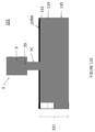
- FIGS 1A-1C illustrate a TFET according to one embodiment of the invention.
- the nanowire preferably includes a broken or staggered gap p-n junction such as an (Al)GaSb/InAs(Sb) radial heterostructure surrounded by a high-k gate dielectric and a wrap gate.
- the nanowire 1 is grown on an n-type source region 3, such as an n-type InAs layer on a substrate and/or an n-type doped InAs region in a substrate.
- the nanowire includes an n-type InAsSb nanowire stem and radial shell portion 5 in contact with the source region and a p-type AlGaSb nanowire upper core portion 7.
- a gate insulating layer such as a high-k dielectric layer (e.g., hafnium oxide, aluminum oxide, tantalum oxide, etc.) 9 surrounds the shell 5.
- a gate electrode 11 is located adjacent to the gate insulating layer 9, such that the gate insulating layer 9 is sandwiched between the gate electrode 11 and the nanowire shell 5.
- the gate electrode 11 is a hollow cylinder shaped wrap gate which completely surrounds the gate insulating layer 9 as shown in Figure 1A .
- the gate electrode 11 may be located adjacent to one or more portions of the gate insulating layer rather than completely surrounding the gate insulating layer.
- a p-type GaSb drain region 13 is located in contact with the core 7 at the upper part of the nanowire 1.
- Source and drain electrodes contact the respective source 3 and drain 13 regions. If desired, the separate source 3 and/or drain 13 regions outside the nanowire 1 may be omitted and the source and drain electrodes may directly contact respective regions 5 and 7 of the nanowire 1 which would function as the respective source and drain regions of the TFET. Furthermore, the position of the n-type and p-type regions may be reversed in the diode and any other suitable semiconductor materials may be used instead of the ones described above.
- the nanowire core comprises an n-type InAsSb core surrounded by a p-type (Al)GaSb shell. In this embodiment, not only is the doping type reversed, but also the corresponding material.
- any other suitable materials may be used for the core and the shell, exemplified but not limited by GaAsSb, GaInAs, InP and/or InPAs.
- the material choice in the core/shell heterostructure provides that the band alignment of the materials is staggered with either or both the conduction and valence band discontinuities ( ⁇ Ec, ⁇ Ev) being between 0.5 and 1.5 Eg, where Eg is the band gap energy (e.g., in units of eV).
- ⁇ Ec, ⁇ Ev the conduction and valence band discontinuities
- band structure engineering may be accomplished by scaling the core/shell dimensions into the quantum regime which allows for precise control of the band alignment.
- carrier transport may be controlled by the discrete energy levels formed in a confined semiconductor allowing for a high selectivity of carriers available for transport. The above considerations may be used for any and/or all of the embodiment devices described herein.
- the electric field 15 from the gate electrode 11 is oriented along the direction of the tunneling current 17 between regions 5 and 7.
- the tunneling current 17 direction between the n-type 5 and the p-type 7 portions of the nanowire diode is substantially parallel to the major substrate surface 3a supporting the nanowire and/or is substantially perpendicular to the surface 11a of the gate electrode 11 which faces the nanowire 1 and the gate insulating layer 9.
- flows in the opposite directions i.e., core to shell versus shell to core
- the InAsSb layer 5 is made sufficiently thin that a quantum well is formed between the gate insulating layer 9 and the core 7. This may allow the transistor to operate in the quantum capacitance limit. In other words, the potential in the InAsSb layer 5 is modulated by the potential from the surrounding gate electrode 11.
- the shell layer 5 is sufficiently thin to form quantized states in the quantum well that effectively increase the energy of the carriers.
- the quantization energy is larger than the energy difference between the conduction and valence band edges in a broken gap heterostructure. This effectively introduces an energy separation between the lowest energy states in the n- and p-side, respectively, acting as a tunneling barrier even for materials combination that have a broken gap band alignment.
- the core is made sufficiently thin to form quantized states that in a similar way increase the energy.
- both the InAs(Sb) layer 5 and the (Al)GaSb layer 7 are sufficiently thin (for example below 20 nm in total thickness, such as 2-15 nm in total thickness) to minimize the tunnel distance and thereby increasing the tunnel current.
- a graded doping profile can be present in the core 7, from a low doping at the interface to the stem 5A to a higher doping towards the drain 13, in order to maintain a uniform voltage drop, and in turn, a uniform tunneling current across the entire tunneling area (the interface between the shell 5 and the core 7).
- the doping is graded in the vertical direction in the device, where the doping concentration is lower in the bottom part than in the top part of the device.
- the device shown in Figure 1B can be fabricated according to the following method. First, an InAs(Sb) nanowire stem 5A is grown on the source region 3. Then, an axial (Al)GaSb heterostructure (i.e., upper nanowire core portion) 7 is grown on the stem 5A. The bottom part of the resulting nanowire (e.g., the stem 5A portion) is then subsequently protected by forming a masking layer 9A, such an electrically insulating layer (e.g., SiN x , HSQ, SiO 2 , etc). A shell 5 of InAs(Sb) is then grown on the nanowire, covering the outside of the nanowire except for bottom portion where the stem 5A is protected by the masking layer 9A.
- a masking layer 9A such an electrically insulating layer (e.g., SiN x , HSQ, SiO 2 , etc).
- a shell 5 of InAs(Sb) is then grown on the nanowire, covering the outside of
- the gate insulating layer 9 and the wrap gate electrode 11 are then formed around the radial nanowire.
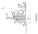
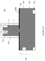
- Figure 2 illustrates an alternative embodiment of a radial nanowire TFET.
- the device comprises at least one nanowire 1 comprising a nanowire core 7 grown on a substrate and at least a first shell layer 5 arranged on the core 7 and at least partly surrounding the nanowire core 5, to provide a radial heterostructure nanowire.
- the core 7 and the shell 5 are preferably made of opposite conductivity type (e.g., if the core 7 is p-type, then the shell 5 is n-type and vice-versa) semiconductor material to form a pn junction.
- an optional intrinsic shell layer may be located between the core 7 and the shell 5 to form a pin junction.
- a gate insulating layer 9 is located around the shell 5 and a gate electrode 11 is located adjacent to the gate insulating layer 9, such as wrapping around the gate insulating layer 9.
- the core 7 (e.g., n-type core) of the radial nanowire 1 may be located in contact with the same conductivity type semiconductor source region 3 (e.g., n-type region) in the substrate.
- a source electrode 19 may be located in contact with region 3 and a drain electrode 21 may be located in contact with the shell 5.
- an optional semiconductor drain region 13 e.g., another shell layer or a quasi-bulk bulb
- the same conductivity type e.g., p-type
- An optional interlayer insulating layer may separate the gate electrode 9 from the source and drain electrodes 19, 21. It should be noted that the barrier "plug" region 7B described below and/or the graded core doping described above may also be added to the device of Figure 2 if desired.
- One non-limiting advantage of the embodiments of the present invention is that the electric field is oriented along the direction of the tunneling current and that the transistor does not necessarily rely on the field effect or depletion.
- a further advantage is that the high-k material 9 will only be in contact with one semiconductor material (e.g., region 5) which simplifies the material integration.
- the gated diode does not require any critical alignment to any heterostructure.
- Another advantage is that the current density may be high and the transistor is formed in a three dimensional array.
- the device does not require as aggressive diameter scaling as an axial device, as the critical dimension is set by the lateral overgrowth on the side facets.
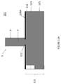
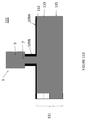
- Figure 3 is a simulation plot of drain current (drain to source current) versus gate voltage (gate to source voltage) for radial and axial TFETs.
- Figures 4 and 5 are simulation plots of drain current (drain to source current) versus gate voltage (gate to source voltage) for respective axial and radial TFETs.
- Figures 6-7 are dimensional plots of a radial TFET of the embodiments of the invention and Figures 8-9 are dimensional plots of an axial TFET of a comparative example. The non-local tunneling rate is shown in Figure 7 in the radial nanowire shell and near the p-n junction in the axial nanowire in Figure 9 .
- Figures 10A and 10B are side cross sectional views of a right side portion of a simulated TFET containing an axial and radial nanowire, respectively, that were used for the respective simulations in Figures 4, 6, 7 and 5, 8, 9 respectively. In other words, Figures 10A and 10B only show the right side of the nanowire to the right of the vertical axis of symmetry.
- the simulated conventional axial nanowire shown in Figure 10A contains a lower p-type semiconductor axial portion 8 over a source region 3 and an upper n-type semiconductor axial portion 6.
- a high-k oxide gate insulating layer 9 surrounds both portions 6, 8 of the nanowire and a wrap gate electrode 11 is located in contact with the gate insulating layer 9 adjacent to the upper portion 6 of the nanowire.
- a drain region 13 is located over portion 6. Portions 6 and 8 form a pn junction of the TFET.
- the nanowire radius is 25 nm
- portion 6 comprises n-type InAs having a donor doping concentration, N D , of 10 17 cm -3
- portion 8 comprises p-type (Al)GaSb having an acceptor doping concentration, N A , of 10 18 cm -3
- the simulated inventive radial nanowire shown in Figure 10B contains a core 7 comprising a lower p-type semiconductor portion 7A over a source region 3 and an upper lightly doped n-type semiconductor portion (e.g., a barrier portion) 7B.
- a heavily doped n-type shell 5 is located around the core 7, such that the shell 5 wraps around the upper portion 7B and at least a top part of the lower portion 7A to form the pn junction of the TFET.
- a high-k oxide gate insulating layer 9 surrounds the shell 5 and a wrap gate electrode 11 is located in contact with the gate insulating layer 9 adjacent to the shell 5.
- An interlayer insulating layer 10 (which can be the same or different form the masking layer 9A shown in Figure 1C ) separates the gate electrode 11 and the shell 5 from the source region 3.
- a drain region 13 is located over portion 6.
- the nanowire core 7 radius is 25 nm, and the nanowire shell 5 radius is 10 nm, such that the entire semiconductor nanowire has a radius of 35 nm.
- the shell 5 comprises n-type InAs having a donor doping concentration, N D , of 10 17 cm -3
- the lower core portion 7A comprises p-type (Al)GaSb having an acceptor doping concentration, N A , of 10 18 cm -3 .
- the upper core portion 7B is optional and comprises n-type InP having a donor doping concentration, N D , of 10 16 cm -3 .
- the barrier portion 7B is provided to keep the TFET current flowing between the core 7A and the shell 5 of the nanowire, this is generally in the horizontal (e.g., radial) direction, along the gate field, where the vertical direction is along the axis of the nanowire core.
- portion 7B can be made of the same semiconductor material as the shell 5 but with lower doping concentration than the shell 5.
- portion 7B may be made of an electrically insulating material or of a different semiconductor material than the shell 5.
- barrier portion 7B has a higher bandgap than both the shell 5 and core portion 7A.
- barrier portion 7B has a higher bandgap than the shell 5 and lower doping level than the core portion 7A.
- the barrier portion 7B in addition to having a larger band gap than the core portion 7A and the shell 5, should have a sufficiently high offset at both the conduction and valence band edge, so that the barrier may efficiently suppress the leakage current.
- the barrier portion 7B may comprise lightly doped, intrinsic, semi-insulating semiconductor material having a doping concentration of 10 16 cm -3 or lower (e.g., unavoidable impurity level to 10 16 cm -3 ) or it may comprise an electrically insulating material.
- Portion 7B may be referred to as a "plug" in the radial nanowire device.
- the nanowire core 7 comprises a first (e.g., lower) semiconductor portion 7A of the first (e.g., p) conductivity type having a first (e.g., high) doping concentration and a second (e.g., upper) portion 7B located in the core adjacent to (e.g., over) the first portion 7A.
- the shell 5 is made of a second (e.g., n) conductivity type semiconductor.
- the upper portion 7B comprises an electrically insulating material or a semiconductor material having a second doping concentration lower than that of lower portion 7A and of the shell 5.
- the lower portion 7A of the core electrically contacts a semiconductor source region 3 of the first (e.g., p) conductivity type and the shell electrically contacts a drain region 13 of the second conductivity type.
- the shell 5 is located adjacent to the upper portion 7B of the core and at least partially overlaps the lower portion 7A of the core to form a pn junction 20.
- the gate electrode 11 at least partially overlaps the pn junction.
- the p-side electrode (not shown for clarity) electrically contacts the source 3 while the n-side electrode (not shown for clarity) electrically contacts the drain region 13.
- the conductivity types e.g., p and n
- FIG 10C illustrates one embodiment of the structure of the device schematically illustrated in Figure 10B .
- the radial tunneling field-effect transistor or gated Esaki diode includes a radial semiconductor nanowire.
- the tunneling current is modulated in the nanowire between a shell 5, and a core 7, which have opposite majority carriers, such as a p-type core and a n-type shell or vice versa.
- the core/shell may be grown on top of a stem 5A of a semiconductor with the same conductivity type as the shell 5, e.g. an n-type stem of InAs would for example be suitable for an n-InAs shell.
- the core 7 would include a blocking barrier 7B for the axial leakage current between the stem 5A and the core portion 7A.
- the blocking barrier 7B may be implemented in the form of a high bandgap semiconductor segment, or as a graded doping profile, which could continue into portion 7A, and in the same material as the core portion 7A.
- the introduction of a barrier segment 7B would fill the purpose of increasing the radial-to-axial tunneling current ratio as described above.
- the source 3 and drain 13 electrodes would be formed to the stem segment 5A of the nanowire and to the core portion 7A.
- Selective etching of the shell 5, on a part of the core/shell segment, at the opposite end of the nanowire, as seen from the stem 5A, would allow for electrode formation directly to the core portion 7A. Passing a current between the stem 5A and/or the shell 5 and the core portion 7A would result in a tunneling current, where the active tunneling interface would be located at the junction between the core portion 7A and shell 5.
- the nanowire would be clad in an isolator such as a high-k dielectric or oxide 9, possibly deposited by atomic layer deposition for conformal coverage.
- the third electrode (the gate) 11 would apply an electric field in parallel to tunneling current between core portion 7A and shell 5.
- the device described above provides a radial tunneling field-effect transistor where the dominating tunneling current is modulated between two segments of the nanowire with different majority carriers, such as e.g. a p-type GaSb core 7 and a n-type InAs shell 5 or vice versa.
- the device provides a radial tunneling contribution to the current and limits the contribution from thermally excited carriers and diffusive transport under biased conditions.
- a barrier 7B introduced between the reservoirs of carriers in the source and drain, where the source 3 can be a n-type InAs buffer layer in series with a n-type InAs nanowire stem 5A connected to a n-type InAs shell 5, and the drain can be all or part of a p-type GaSb core 7A connected to a metal electrode 13.
- the barrier or "plug” 7B may comprise of a high bandgap semiconductor, such as GaAs or InP, or a graded semiconductor and minimizes the leakage currents perpendicular to an applied electric field from the gate, where the gate is positioned so that the dominating tunneling current is parallel to the electric field applied by the gate, i.e., radial tunneling.
- a high bandgap semiconductor such as GaAs or InP
- a graded semiconductor minimizes the leakage currents perpendicular to an applied electric field from the gate, where the gate is positioned so that the dominating tunneling current is parallel to the electric field applied by the gate, i.e., radial tunneling.
- underlap means that the gate electrode 11 does not reach the (Al)GaSb lower portion 8 of the nanowire by the noted amount in the Figure (i.e., the gate electrode is located above the pn junction). Overlap means that the gate electrode 11 reaches down over the (Al)GaSb lower portion 8 of the nanowire by the noted amount in Figure 4 (i.e., the gate electrode extends below the pn junction).
- underlap means that the gate electrode 11 does not reach the end (i.e., the bottom) of the InAs shell 5, while overlap means that the gate electrode 11 reaches below the InAs shell 5.
- the device shown in Figure 10B is a preferred embodiment. This structure provides the following advantages compared to the prior art.
- the upper nanowire "plug" portion 7B blocks the usual large lateral generation of tunnel carriers (parallel to the applied source-drain field).
- the shell 5 with the drain contact 13 together with the GaSb core portion 7A provides a very steep, radial pn junction (broken or staggered gap alignment) depending on core diameter and shell thickness, doping levels, and material composition (e.g., amount of Sb and Al).
- the wrap gate 11 forces a field perpendicular to the pn-junction so that the total electric field across the junction (source-drain and gate field) is essentially perpendicular to the pn-junction.
- the parallel part of the field comprises the source-drain potential.
- the almost stepwise change in Fermi level across the junction induced in this way allows a sub-thermal tunnel generation of carriers that provides a sub-60 mV/dec. sub-threshold swing and a high tunnel current.
- solar cell 101 includes a planar pn or pin junction solar cell 131 portion and a radial Esaki diode 1 portion upstanding on the planar solar cell 131 upper surface 132.
- the longitudinal axis of the diode 1 may extend perpendicular to the upper surface 132 of the planar solar cell 131.
- the planar solar cell may comprise a first region (e.g., upper region or layer) 133 of a first conductivity type (e.g., n-type) and a second region (e.g., lower region or layer) 135 of a second conductivity type (e.g., p-type). Regions 133 and 135 form a pn junction. If desired, an intrinsic layer may be located between regions 133 and 135 to form a pin junction.
- the second region 135 may comprise a doped semiconductor substrate, a doped region in the semiconductor substrate or a doped semiconductor layer formed over a semiconductor, conductive (e.g., metal) or insulating (e.g., ceramic, plastic, glass, quartz, etc.) substrate (not shown for clarity).
- the first region 133 may comprise a doped region in the semiconductor substrate or a doped semiconductor layer formed over the second region 135.
- Regions 133 and 135 may comprise any type of semiconductor, such as an inorganic semiconductor, for example Group IV (e.g., silicon, germanium, SiGe, etc.), Group III-V (e.g., GaAs, InP, etc.) or Group II-VI (e.g., CdTe, etc.) semiconductor.
- region 133 may be n-type silicon and region 135 may be p-type silicon.
- the upper surface 132 of the planar solar cell 131 may comprise an electrically insulating masking layer 109A, such as silicon nitride, silicon oxide, etc.
- layer 109A is transparent to solar radiation, especially of wavelengths above the wavelengths absorbed in the solar cell junction formed by the core 7 and the shell 5.
- the nanowire 1 protrudes through an opening 111 in the masking layer 109A.
- the nanowire 1 core 7 may be grown on semiconductor region 133 exposed through the opening 111 without using a catalyst as described above. Alternatively, the nanowire 1 core 7 may be first grown on the upper surface 132 of region 133 using a metal catalyst particle, or via selective area growth, followed by the formation of the masking layer 109A around the nanowire core and then the growth of the shell 5 around the exposed core 7, as also described above.
- the nanowire core 7 and the first region 133 of the planar solar cell 131 contact each other and have the same conductivity type (e.g., n-type).
- the shell 5 and the second region 135 of the planar solar cell 131 do not contact each other and have the same conductivity type (e.g., p-type) different from that of the core 7 and the first region 133.
- the structure shown in Figure 11A forms two pn junctions of a multi-junction planar/nanowire hybrid solar cell, where the nanowire junction is preferably III/V semiconductor based and the substrate (e.g., planar solar cell) junction is Si based.
- the core and shell regions may comprise III-V materials, such as GaAs/InP for example.
- the radial nanowire Esaki diode is a "circumventing" (e.g., circumferential) heterostructure Esaki diode utilizing heavily doped n++/p++ core/shell region and a band gap heterostructure discontinuity for improved performance.
- the Esaki band pass polarity inversion is advantageous in retaining band energy from carriers excited in the high energy bandgap nanowire solar cell. This also provides the advantage for matching Esaki diode area to the junction excitation volumes, in order to facilitate critical current matching between the junctions. This is especially advantageous over using axial nanowire Esaki diodes.
- Figure 11B illustrates another embodiment of the multi-junction solar cell 101 in which the shell 5 comprises a bulb or a quasi-bulk region at the top part of the core 7. If desired, an additional masking layer 109B may be formed between the shell 5 and the first masking layer 109A.
- Figure 11C illustrates another embodiment multi-junction solar cell 101 in which the core 7 comprises a heterostructure containing lower 7C and upper 7D regions composed of different III-V semiconductor materials, and/or different doping levels, of the first conductivity type, of special value for the gated TFET applications described above.
- Figure 11D illustrates the connection of the n-side electrode 141 and p-side electrode 143 to the solar cell 101.
- an additional shell layer, bulk or quasi-bulk region 113 of the first conductivity type e.g., n-type
- the shell 5 of the second conductivity type e.g., p-type
- the radial sequence in the nanowire will consist of (in this version): n++/p++/p/i/n/n+ regions, where the first n++/p++ junction constitutes the Esaki tunnel diode, the p/i/n diode is the active, large band-gap solar cell, and the n+ layer is for providing the contact surface layer of the nanowire solar cell.
- Electrode 141 is then formed in contact with region 113. If the nanowire side of the solar cell 101 will be exposed to solar radiation, then electrode 141 is made of an electrically conductive material that is substantially transparent to solar radiation, such as a transparent conductive oxide (TCO), for example, indium tin oxide, zinc oxide, etc.
- TCO transparent conductive oxide
- the p-side electrode 143 is formed in contact with region 135 of the planar solar cell 131. Electrode 143 may be made of any suitable metal, such as Al, Cu, Ti, Ag, etc. and their alloys.
- the Esaki diode forms the "third junction" of the multi-junction solar cell 101, switching the polarity of the carriers in order to put the planar and the radial junctions in series without any metallic contact that would divert, or spill the "local entropy" that the bandgap height retains for the carriers.
- the conductivity type of the semiconductor regions may be reversed.
- one nanowire 1 is illustrated, it should be understood that a large number (e.g., plurality) of nanowires are formed on the planar solar cell 131, in such a way that (virtually) all photons are trapped by the wire array such that the substrate pn-junction is only exposed to photons that passed through the nanowire pn-junction with the higher band-gap.
- Figures 12A and 12B illustrate temperature dependent characteristics of an Esaki diode according to an embodiment of the invention.
- Figure 12A is a plot of current versus voltage as a function of temperature and
- PVCR peak-to-valley current ratio
- the plot includes a dip (i.e., valley) in current as a function of voltage, at all measured temperatures between 4.2K and 295K. This is characteristic of a negative differential resistance and Esaki tunneling diode behavior.
- Figure 12B illustrates that the PVCR is above 10 for all measured temperatures of 295K and lower (e.g., a PVCR of above 10, such as 11 to 14, at about room temperature of 295K), and the PVCR is above 100, such as 101 to 105 at lower temperatures (e.g., below 60K, such as at 4.2-30K).
- a PVCR of above 10 such as 11 to 14, at about room temperature of 295K
- the PVCR is above 100, such as 101 to 105 at lower temperatures (e.g., below 60K, such as at 4.2-30K).
- the diode comprises a n-type, heavily sulfur-doped InP core and a heavily Zn-doped InGaAs shell.
- This material combination may be used for the core and the shell, exemplified but not limited by GaAsSb, GaInAs, InP, and/or InPAs, in any and/or all embodiment devices described above.
- band structure engineering may be accomplished by scaling the core/shell dimensions into the quantum regime which allows for precise control of the band alignment.
- carrier transport may be controlled by the discrete energy levels formed in a confined semiconductor allowing for a high selectivity of carriers available for transport.
Landscapes
- Engineering & Computer Science (AREA)
- Power Engineering (AREA)
- Microelectronics & Electronic Packaging (AREA)
- Physics & Mathematics (AREA)
- Condensed Matter Physics & Semiconductors (AREA)
- General Physics & Mathematics (AREA)
- Computer Hardware Design (AREA)
- Ceramic Engineering (AREA)
- Chemical & Material Sciences (AREA)
- Nanotechnology (AREA)
- Crystallography & Structural Chemistry (AREA)
- Materials Engineering (AREA)
- Electromagnetism (AREA)
- Life Sciences & Earth Sciences (AREA)
- Mathematical Physics (AREA)
- Theoretical Computer Science (AREA)
- Sustainable Development (AREA)
- Sustainable Energy (AREA)
- Thin Film Transistor (AREA)
- Photovoltaic Devices (AREA)
- Insulated Gate Type Field-Effect Transistor (AREA)
- Junction Field-Effect Transistors (AREA)
Claims (7)
- Dispositif comprenant un transistor à effet de champ à effet tunnel (TFET) à grille comportant une diode Esaki à nanofil radial à grille, dans lequel le nanofil radial vertical (7, 5) comprend une âme semi-conductrice (7A, 7B) d'un premier type de conductivité, une coque semi-conductrice (5) d'un second type de conductivité différent du premier type de conductivité, une couche isolante de grille (9) autour de la coque, et une électrode de grille (11) située adjacente à la couche isolante de grille.
- Dispositif selon la revendication 1, le dispositif étant structuré de telle sorte qu'en service le sens du courant d'effet tunnel entre l'âme et la coque soit sensiblement parallèle à une surface principale d'un substrat supportant le nanofil et soit sensiblement perpendiculaire à une surface de l'électrode de grille qui fait face au nanofil et à la couche isolante de grille, et dans lequel le sens du courant à effet tunnel entre l'âme et la coque est sensiblement parallèle à un sens de champ électrique de grille.
- Dispositif selon la revendication 2, dans lequel :l'âme de nanofil comprend une partie semi-conductrice inférieure (7A) du premier type de conductivité ayant une première concentration de dopage et une partie supérieure (7B) située pardessus la partie inférieure ;la partie supérieure comprend un matériau électriquement isolant (figure 10C) ou un semi-conducteur (figure 10B) ayant une seconde concentration de dopage inférieure à la première concentration de dopage de la partie inférieure etinférieure à une concentration de dopage de la coque ;la partie inférieure de l'âme (7A) fait contact électriquement avec une région de source semi-conductrice (3) du premier type de conductivité et la coque (5) fait contact électriquement avec une région de drain (13) du second type de conductivité ;la coque (5) est située adjacente à la partie supérieure (7B) de l'âme et chevauche au moins partiellement la partie inférieure (7A) de l'âme pour former une jonction pn etl'électrode de grille chevauche au moins partiellement la jonction pn.
- Dispositif selon la revendication 2, dans lequel :un puits quantique est formé dans la coque entre la couche isolante de grille et l'âme.
- Dispositif selon la revendication 2, comprenant en outre une région barrière située entre l'âme et au moins l'une d'une région de source et d'une région de drain du TFET, dans lequel :le matériau de la région barrière a une bande interdite supérieure à celle à la fois du matériau d'âme semi-conductrice et du matériau de coque semi-conductrice ; etla région barrière comprend un matériau électriquement isolant ou un matériau semi-conducteur légèrement dopé, intrinsèque ou semi-isolant ayant une concentration de dopage de 1016 cm-3 ou inférieure.
- Procédé d'exploitation d'un transistor à effet de champ à effet tunnel (TFET) à grille comportant une diode Esaki à grille comprenant un nanofil semi-conducteur radial vertical (7, 5) comprenant une âme semi-conductrice (7) d'un premier type de conductivité, une coque semi-conductrice (5) d'un second type de conductivité différent du premier type de conductivité, une couche isolante de grille (9) située autour de la coque, et une électrode de grille (11) située adjacente à la couche isolante de grille, dans lequel un courant d'effet tunnel entre l'âme et la coque dopées de manière opposée du nanofil semi-conducteur radial s'écoule sensiblement parallèlement à un champ électrique fourni par l'électrode de grille au nanofil semi-conducteur radial.
- Procédé selon la revendication 8, dans lequel le courant d'effet tunnel entre l'âme et la coque s'écoule sensiblement parallèlement à une surface principale d'un substrat supportant le nanofil. l'âme de nanofil comprend une partie semi-conductrice inférieure (7A) du premier type de conductivité ayant une première concentration de dopage et une partie supérieure (7B) située pardessus la partie inférieure ;
la partie supérieure comprend un matériau électriquement isolant ou un matériau semi-conducteur ayant une seconde concentration de dopage inférieure à la première concentration de dopage de la partie inférieure et inférieure à une concentration de dopage de la coque ;
la partie inférieure de l'âme fait contact électriquement avec une région de source semi-conductrice (3) du premier type de conductivité et la coque fait contact électriquement avec une région de drain du second type de conductivité ;
la coque (5) est située adjacente à la partie supérieure de l'âme et chevauche au moins partiellement la partie inférieure de l'âme pour former une jonction pn ;
l'électrode de grille (11) chevauche au moins partiellement la jonction pn ;
la partie supérieure de l'âme (7B) bloque une génération latérale importante de porteurs d'effet tunnel parallèles à un champ source-drain appliqué ;
l'électrode de grille fournit un champ perpendiculaire à la jonction pn de telle sorte qu'un champ électrique total en travers de la jonction pn comprenant une source-drain et un champ de grille soit essentiellement perpendiculaire à la jonction pn ;
le niveau de Fermi est sensiblement constant des deux côtés de la jonction pn ; et
un changement induit sensiblement par pas du niveau de Fermi en travers de la jonction pn fournit une génération de porteurs par effet tunnel sous-thermique qui produit une pente sous le seuil inférieure à 60 mV/dec.
Applications Claiming Priority (2)
| Application Number | Priority Date | Filing Date | Title |
|---|---|---|---|
| US201261668777P | 2012-07-06 | 2012-07-06 | |
| PCT/IB2013/001856 WO2014006503A2 (fr) | 2012-07-06 | 2013-07-05 | Dispositifs diodes esaki à nanofil radial et procédés associés |
Publications (3)
| Publication Number | Publication Date |
|---|---|
| EP2870632A2 EP2870632A2 (fr) | 2015-05-13 |
| EP2870632A4 EP2870632A4 (fr) | 2016-03-09 |
| EP2870632B1 true EP2870632B1 (fr) | 2016-10-26 |
Family
ID=49882532
Family Applications (1)
| Application Number | Title | Priority Date | Filing Date |
|---|---|---|---|
| EP13813238.6A Not-in-force EP2870632B1 (fr) | 2012-07-06 | 2013-07-05 | Dispositifs diodes radiales esaki à nanofil et procédés associés |
Country Status (6)
| Country | Link |
|---|---|
| US (1) | US10090292B2 (fr) |
| EP (1) | EP2870632B1 (fr) |
| JP (1) | JP6290199B2 (fr) |
| KR (1) | KR20150036229A (fr) |
| CN (1) | CN104603952B (fr) |
| WO (1) | WO2014006503A2 (fr) |
Families Citing this family (15)
| Publication number | Priority date | Publication date | Assignee | Title |
|---|---|---|---|---|
| US8916927B2 (en) * | 2012-07-19 | 2014-12-23 | Taiwan Semiconductor Manufacturing | Vertical tunnel field effect transistor (FET) |
| SE1530097A1 (en) * | 2015-06-22 | 2016-12-23 | Method for Vertical Gate-Last Process | |
| US9748379B2 (en) * | 2015-06-25 | 2017-08-29 | Taiwan Semiconductor Manufacturing Co., Ltd. | Double exponential mechanism controlled transistor |
| US10381489B2 (en) * | 2015-09-30 | 2019-08-13 | National University Corporation Hokkaido University | Tunnel field effect trasnsistor |
| JP6730598B2 (ja) * | 2016-07-19 | 2020-07-29 | 富士通株式会社 | 半導体装置 |
| JP6741943B2 (ja) * | 2016-08-31 | 2020-08-19 | 富士通株式会社 | 半導体装置及びその製造方法 |
| US10475673B2 (en) * | 2016-09-28 | 2019-11-12 | Stmicroelectronics S.R.L. | Apparatus for manufacturing a silicon carbide wafer |
| JP6631458B2 (ja) * | 2016-09-29 | 2020-01-15 | 富士通株式会社 | 電子デバイス及びその製造方法 |
| US10325993B2 (en) * | 2017-09-28 | 2019-06-18 | Taiwan Semiconductor Manufacturing Co., Ltd. | Gate all around device and fabrication thereof |
| US10868157B2 (en) * | 2018-09-26 | 2020-12-15 | Taiwan Semiconductor Manufacturing Co., Ltd. | Gated metal-insulator-semiconductor (MIS) tunnel diode having negative transconductance |
| US11309177B2 (en) | 2018-11-06 | 2022-04-19 | Stmicroelectronics S.R.L. | Apparatus and method for manufacturing a wafer |
| JP7371366B2 (ja) * | 2019-06-27 | 2023-10-31 | 富士通株式会社 | 半導体デバイス、及びこれを用いた無線受信器 |
| IT201900015416A1 (it) | 2019-09-03 | 2021-03-03 | St Microelectronics Srl | Apparecchio per la crescita di una fetta di materiale semiconduttore, in particolare di carburo di silicio, e procedimento di fabbricazione associato |
| WO2021210095A1 (fr) | 2020-04-15 | 2021-10-21 | 富士通株式会社 | Dispositif à semi-conducteur, système de calcul de réservoir et procédé de fabrication de dispositif à semi-conducteur |
| JP7176700B2 (ja) * | 2020-07-31 | 2022-11-22 | セイコーエプソン株式会社 | 発光装置およびプロジェクター |
Family Cites Families (14)
| Publication number | Priority date | Publication date | Assignee | Title |
|---|---|---|---|---|
| US7335908B2 (en) | 2002-07-08 | 2008-02-26 | Qunano Ab | Nanostructures and methods for manufacturing the same |
| JP5255437B2 (ja) | 2005-06-16 | 2013-08-07 | クナノ アーベー | 半導体ナノワイヤトランジスタ |
| US20070052012A1 (en) * | 2005-08-24 | 2007-03-08 | Micron Technology, Inc. | Vertical tunneling nano-wire transistor |
| EP1892769A2 (fr) * | 2006-08-25 | 2008-02-27 | General Electric Company | Dispositifs photovoltaïques à nanofils à jonction conforme unique |
| US7893476B2 (en) * | 2006-09-15 | 2011-02-22 | Imec | Tunnel effect transistors based on silicon nanowires |
| US8049203B2 (en) * | 2006-12-22 | 2011-11-01 | Qunano Ab | Nanoelectronic structure and method of producing such |
| WO2008079077A2 (fr) * | 2006-12-22 | 2008-07-03 | Qunano Ab | Structure nanoélectronique et procédé de production associé |
| US7977568B2 (en) | 2007-01-11 | 2011-07-12 | General Electric Company | Multilayered film-nanowire composite, bifacial, and tandem solar cells |
| CA2674448A1 (fr) | 2007-01-12 | 2008-07-17 | Qunano Ab | Nanofils de nitrure et leur procede de fabrication |
| WO2008156421A2 (fr) | 2007-06-19 | 2008-12-24 | Qunano Ab | Structure de cellule solaire à nanofil |
| KR20100137566A (ko) | 2008-04-15 | 2010-12-30 | 큐나노 에이비 | 나노와이어 랩 게이트 디바이스들 |
| WO2010120233A2 (fr) * | 2009-04-15 | 2010-10-21 | Sol Voltaics Ab | Cellule photovoltaïque multi-jonction avec nanofils |
| JP5652827B2 (ja) * | 2009-09-30 | 2015-01-14 | 国立大学法人北海道大学 | トンネル電界効果トランジスタおよびその製造方法 |
| EP2491595A4 (fr) | 2009-10-22 | 2014-03-19 | Sol Voltaics Ab | Diode à effet tunnel à nanocâble et procédé de fabrication de celle-ci |
-
2013
- 2013-07-05 EP EP13813238.6A patent/EP2870632B1/fr not_active Not-in-force
- 2013-07-05 WO PCT/IB2013/001856 patent/WO2014006503A2/fr active Application Filing
- 2013-07-05 US US14/407,007 patent/US10090292B2/en not_active Expired - Fee Related
- 2013-07-05 KR KR20157002218A patent/KR20150036229A/ko not_active Application Discontinuation
- 2013-07-05 JP JP2015519381A patent/JP6290199B2/ja not_active Expired - Fee Related
- 2013-07-05 CN CN201380036099.4A patent/CN104603952B/zh not_active Expired - Fee Related
Non-Patent Citations (1)
| Title |
|---|
| None * |
Also Published As
| Publication number | Publication date |
|---|---|
| JP2015529006A (ja) | 2015-10-01 |
| US20150171076A1 (en) | 2015-06-18 |
| US10090292B2 (en) | 2018-10-02 |
| EP2870632A2 (fr) | 2015-05-13 |
| CN104603952A (zh) | 2015-05-06 |
| EP2870632A4 (fr) | 2016-03-09 |
| WO2014006503A2 (fr) | 2014-01-09 |
| WO2014006503A3 (fr) | 2014-03-13 |
| KR20150036229A (ko) | 2015-04-07 |
| CN104603952B (zh) | 2017-07-21 |
| JP6290199B2 (ja) | 2018-03-07 |
Similar Documents
| Publication | Publication Date | Title |
|---|---|---|
| EP2870632B1 (fr) | Dispositifs diodes radiales esaki à nanofil et procédés associés | |
| US9096429B2 (en) | Nanoelectronic structure and method of producing such | |
| US8692301B2 (en) | Nanostructured photodiode | |
| US9136363B2 (en) | Compound tunneling field effect transistor integrated on silicon substrate and method for fabricating the same | |
| JP6600918B2 (ja) | トンネル電界効果トランジスタ | |
| US20130264544A1 (en) | Nanowire field-effect device with multiple gates | |
| US20120199187A1 (en) | Nanowire tunnel diode and method for making the same | |
| KR20100137566A (ko) | 나노와이어 랩 게이트 디바이스들 | |
| US9312377B2 (en) | Semiconductor devices and methods of manufacturing the same | |
| TWI630719B (zh) | 磊晶再成長之異質結構奈米線側向穿隧場效電晶體 | |
| KR101458566B1 (ko) | 정류소자 및 그의 제조 방법 | |
| WO2023182099A1 (fr) | Transistor à effet de champ et élément de commutation |
Legal Events
| Date | Code | Title | Description |
|---|---|---|---|
| PUAI | Public reference made under article 153(3) epc to a published international application that has entered the european phase |
Free format text: ORIGINAL CODE: 0009012 |
|
| 17P | Request for examination filed |
Effective date: 20150129 |
|
| AK | Designated contracting states |
Kind code of ref document: A2 Designated state(s): AL AT BE BG CH CY CZ DE DK EE ES FI FR GB GR HR HU IE IS IT LI LT LU LV MC MK MT NL NO PL PT RO RS SE SI SK SM TR |
|
| AX | Request for extension of the european patent |
Extension state: BA ME |
|
| DAX | Request for extension of the european patent (deleted) | ||
| A4 | Supplementary search report drawn up and despatched |
Effective date: 20160204 |
|
| RIC1 | Information provided on ipc code assigned before grant |
Ipc: H01L 29/06 20060101ALI20160129BHEP Ipc: B82Y 10/00 20110101ALI20160129BHEP Ipc: H01L 29/739 20060101ALI20160129BHEP Ipc: H01L 31/0693 20120101ALI20160129BHEP Ipc: H01L 29/885 20060101AFI20160129BHEP Ipc: H01L 29/78 20060101ALI20160129BHEP |
|
| RIC1 | Information provided on ipc code assigned before grant |
Ipc: H01L 29/06 20060101ALI20160630BHEP Ipc: H01L 29/885 20060101AFI20160630BHEP Ipc: B82Y 10/00 20110101ALI20160630BHEP Ipc: H01L 31/06 20120101ALI20160630BHEP Ipc: H01L 27/06 20060101ALI20160630BHEP Ipc: H01L 29/739 20060101ALI20160630BHEP Ipc: H01L 29/78 20060101ALI20160630BHEP |
|
| GRAP | Despatch of communication of intention to grant a patent |
Free format text: ORIGINAL CODE: EPIDOSNIGR1 |
|
| RIC1 | Information provided on ipc code assigned before grant |
Ipc: H01L 29/78 20060101ALI20160712BHEP Ipc: H01L 29/885 20060101AFI20160712BHEP Ipc: H01L 29/06 20060101ALI20160712BHEP Ipc: H01L 31/06 20120101ALI20160712BHEP Ipc: H01L 29/739 20060101ALI20160712BHEP Ipc: H01L 31/0352 20060101ALI20160712BHEP Ipc: B82Y 10/00 20110101ALI20160712BHEP |
|
| INTG | Intention to grant announced |
Effective date: 20160805 |
|
| RIN1 | Information on inventor provided before grant (corrected) |
Inventor name: THELANDER, CLAES Inventor name: DEY, ANIL Inventor name: WERNERSSON, LARS-ERIK Inventor name: SAMUELSON, LARS Inventor name: LIND, ERIK Inventor name: BJOERK, MIKAEL Inventor name: OHLSSON, JONAS |
|
| GRAS | Grant fee paid |
Free format text: ORIGINAL CODE: EPIDOSNIGR3 |
|
| GRAA | (expected) grant |
Free format text: ORIGINAL CODE: 0009210 |
|
| AK | Designated contracting states |
Kind code of ref document: B1 Designated state(s): AL AT BE BG CH CY CZ DE DK EE ES FI FR GB GR HR HU IE IS IT LI LT LU LV MC MK MT NL NO PL PT RO RS SE SI SK SM TR |
|
| REG | Reference to a national code |
Ref country code: GB Ref legal event code: FG4D |
|
| REG | Reference to a national code |
Ref country code: CH Ref legal event code: EP |
|
| REG | Reference to a national code |
Ref country code: AT Ref legal event code: REF Ref document number: 840569 Country of ref document: AT Kind code of ref document: T Effective date: 20161115 |
|
| REG | Reference to a national code |
Ref country code: IE Ref legal event code: FG4D |
|
| REG | Reference to a national code |
Ref country code: DE Ref legal event code: R096 Ref document number: 602013013333 Country of ref document: DE |
|
| REG | Reference to a national code |
Ref country code: LT Ref legal event code: MG4D |
|
| PG25 | Lapsed in a contracting state [announced via postgrant information from national office to epo] |
Ref country code: LV Free format text: LAPSE BECAUSE OF FAILURE TO SUBMIT A TRANSLATION OF THE DESCRIPTION OR TO PAY THE FEE WITHIN THE PRESCRIBED TIME-LIMIT Effective date: 20161026 |
|
| REG | Reference to a national code |
Ref country code: NL Ref legal event code: MP Effective date: 20161026 |
|
| REG | Reference to a national code |
Ref country code: AT Ref legal event code: MK05 Ref document number: 840569 Country of ref document: AT Kind code of ref document: T Effective date: 20161026 |
|
| PG25 | Lapsed in a contracting state [announced via postgrant information from national office to epo] |
Ref country code: SE Free format text: LAPSE BECAUSE OF FAILURE TO SUBMIT A TRANSLATION OF THE DESCRIPTION OR TO PAY THE FEE WITHIN THE PRESCRIBED TIME-LIMIT Effective date: 20161026 Ref country code: GR Free format text: LAPSE BECAUSE OF FAILURE TO SUBMIT A TRANSLATION OF THE DESCRIPTION OR TO PAY THE FEE WITHIN THE PRESCRIBED TIME-LIMIT Effective date: 20170127 Ref country code: LT Free format text: LAPSE BECAUSE OF FAILURE TO SUBMIT A TRANSLATION OF THE DESCRIPTION OR TO PAY THE FEE WITHIN THE PRESCRIBED TIME-LIMIT Effective date: 20161026 Ref country code: NO Free format text: LAPSE BECAUSE OF FAILURE TO SUBMIT A TRANSLATION OF THE DESCRIPTION OR TO PAY THE FEE WITHIN THE PRESCRIBED TIME-LIMIT Effective date: 20170126 |
|
| PG25 | Lapsed in a contracting state [announced via postgrant information from national office to epo] |
Ref country code: AT Free format text: LAPSE BECAUSE OF FAILURE TO SUBMIT A TRANSLATION OF THE DESCRIPTION OR TO PAY THE FEE WITHIN THE PRESCRIBED TIME-LIMIT Effective date: 20161026 Ref country code: HR Free format text: LAPSE BECAUSE OF FAILURE TO SUBMIT A TRANSLATION OF THE DESCRIPTION OR TO PAY THE FEE WITHIN THE PRESCRIBED TIME-LIMIT Effective date: 20161026 Ref country code: ES Free format text: LAPSE BECAUSE OF FAILURE TO SUBMIT A TRANSLATION OF THE DESCRIPTION OR TO PAY THE FEE WITHIN THE PRESCRIBED TIME-LIMIT Effective date: 20161026 Ref country code: NL Free format text: LAPSE BECAUSE OF FAILURE TO SUBMIT A TRANSLATION OF THE DESCRIPTION OR TO PAY THE FEE WITHIN THE PRESCRIBED TIME-LIMIT Effective date: 20161026 Ref country code: RS Free format text: LAPSE BECAUSE OF FAILURE TO SUBMIT A TRANSLATION OF THE DESCRIPTION OR TO PAY THE FEE WITHIN THE PRESCRIBED TIME-LIMIT Effective date: 20161026 Ref country code: FI Free format text: LAPSE BECAUSE OF FAILURE TO SUBMIT A TRANSLATION OF THE DESCRIPTION OR TO PAY THE FEE WITHIN THE PRESCRIBED TIME-LIMIT Effective date: 20161026 Ref country code: PT Free format text: LAPSE BECAUSE OF FAILURE TO SUBMIT A TRANSLATION OF THE DESCRIPTION OR TO PAY THE FEE WITHIN THE PRESCRIBED TIME-LIMIT Effective date: 20170227 Ref country code: BE Free format text: LAPSE BECAUSE OF FAILURE TO SUBMIT A TRANSLATION OF THE DESCRIPTION OR TO PAY THE FEE WITHIN THE PRESCRIBED TIME-LIMIT Effective date: 20161026 Ref country code: IS Free format text: LAPSE BECAUSE OF FAILURE TO SUBMIT A TRANSLATION OF THE DESCRIPTION OR TO PAY THE FEE WITHIN THE PRESCRIBED TIME-LIMIT Effective date: 20170226 Ref country code: PL Free format text: LAPSE BECAUSE OF FAILURE TO SUBMIT A TRANSLATION OF THE DESCRIPTION OR TO PAY THE FEE WITHIN THE PRESCRIBED TIME-LIMIT Effective date: 20161026 |
|
| REG | Reference to a national code |
Ref country code: DE Ref legal event code: R097 Ref document number: 602013013333 Country of ref document: DE |
|
| PG25 | Lapsed in a contracting state [announced via postgrant information from national office to epo] |
Ref country code: EE Free format text: LAPSE BECAUSE OF FAILURE TO SUBMIT A TRANSLATION OF THE DESCRIPTION OR TO PAY THE FEE WITHIN THE PRESCRIBED TIME-LIMIT Effective date: 20161026 Ref country code: RO Free format text: LAPSE BECAUSE OF FAILURE TO SUBMIT A TRANSLATION OF THE DESCRIPTION OR TO PAY THE FEE WITHIN THE PRESCRIBED TIME-LIMIT Effective date: 20161026 Ref country code: CZ Free format text: LAPSE BECAUSE OF FAILURE TO SUBMIT A TRANSLATION OF THE DESCRIPTION OR TO PAY THE FEE WITHIN THE PRESCRIBED TIME-LIMIT Effective date: 20161026 Ref country code: DK Free format text: LAPSE BECAUSE OF FAILURE TO SUBMIT A TRANSLATION OF THE DESCRIPTION OR TO PAY THE FEE WITHIN THE PRESCRIBED TIME-LIMIT Effective date: 20161026 Ref country code: SK Free format text: LAPSE BECAUSE OF FAILURE TO SUBMIT A TRANSLATION OF THE DESCRIPTION OR TO PAY THE FEE WITHIN THE PRESCRIBED TIME-LIMIT Effective date: 20161026 |
|
| PG25 | Lapsed in a contracting state [announced via postgrant information from national office to epo] |
Ref country code: IT Free format text: LAPSE BECAUSE OF FAILURE TO SUBMIT A TRANSLATION OF THE DESCRIPTION OR TO PAY THE FEE WITHIN THE PRESCRIBED TIME-LIMIT Effective date: 20161026 Ref country code: BG Free format text: LAPSE BECAUSE OF FAILURE TO SUBMIT A TRANSLATION OF THE DESCRIPTION OR TO PAY THE FEE WITHIN THE PRESCRIBED TIME-LIMIT Effective date: 20170126 Ref country code: SM Free format text: LAPSE BECAUSE OF FAILURE TO SUBMIT A TRANSLATION OF THE DESCRIPTION OR TO PAY THE FEE WITHIN THE PRESCRIBED TIME-LIMIT Effective date: 20161026 |
|
| PLBE | No opposition filed within time limit |
Free format text: ORIGINAL CODE: 0009261 |
|
| STAA | Information on the status of an ep patent application or granted ep patent |
Free format text: STATUS: NO OPPOSITION FILED WITHIN TIME LIMIT |
|
| 26N | No opposition filed |
Effective date: 20170727 |
|
| PG25 | Lapsed in a contracting state [announced via postgrant information from national office to epo] |
Ref country code: SI Free format text: LAPSE BECAUSE OF FAILURE TO SUBMIT A TRANSLATION OF THE DESCRIPTION OR TO PAY THE FEE WITHIN THE PRESCRIBED TIME-LIMIT Effective date: 20161026 |
|
| REG | Reference to a national code |
Ref country code: DE Ref legal event code: R119 Ref document number: 602013013333 Country of ref document: DE |
|
| REG | Reference to a national code |
Ref country code: CH Ref legal event code: PL |
|
| GBPC | Gb: european patent ceased through non-payment of renewal fee |
Effective date: 20170705 |
|
| REG | Reference to a national code |
Ref country code: IE Ref legal event code: MM4A |
|
| REG | Reference to a national code |
Ref country code: FR Ref legal event code: ST Effective date: 20180330 |
|
| PG25 | Lapsed in a contracting state [announced via postgrant information from national office to epo] |
Ref country code: CH Free format text: LAPSE BECAUSE OF NON-PAYMENT OF DUE FEES Effective date: 20170731 Ref country code: LI Free format text: LAPSE BECAUSE OF NON-PAYMENT OF DUE FEES Effective date: 20170731 Ref country code: DE Free format text: LAPSE BECAUSE OF NON-PAYMENT OF DUE FEES Effective date: 20180201 Ref country code: IE Free format text: LAPSE BECAUSE OF NON-PAYMENT OF DUE FEES Effective date: 20170705 Ref country code: GB Free format text: LAPSE BECAUSE OF NON-PAYMENT OF DUE FEES Effective date: 20170705 |
|
| PG25 | Lapsed in a contracting state [announced via postgrant information from national office to epo] |
Ref country code: FR Free format text: LAPSE BECAUSE OF NON-PAYMENT OF DUE FEES Effective date: 20170731 |
|
| PG25 | Lapsed in a contracting state [announced via postgrant information from national office to epo] |
Ref country code: LU Free format text: LAPSE BECAUSE OF NON-PAYMENT OF DUE FEES Effective date: 20170705 |
|
| PG25 | Lapsed in a contracting state [announced via postgrant information from national office to epo] |
Ref country code: MT Free format text: LAPSE BECAUSE OF NON-PAYMENT OF DUE FEES Effective date: 20170705 |
|
| PG25 | Lapsed in a contracting state [announced via postgrant information from national office to epo] |
Ref country code: MC Free format text: LAPSE BECAUSE OF FAILURE TO SUBMIT A TRANSLATION OF THE DESCRIPTION OR TO PAY THE FEE WITHIN THE PRESCRIBED TIME-LIMIT Effective date: 20161026 Ref country code: HU Free format text: LAPSE BECAUSE OF FAILURE TO SUBMIT A TRANSLATION OF THE DESCRIPTION OR TO PAY THE FEE WITHIN THE PRESCRIBED TIME-LIMIT; INVALID AB INITIO Effective date: 20130705 |
|
| PG25 | Lapsed in a contracting state [announced via postgrant information from national office to epo] |
Ref country code: CY Free format text: LAPSE BECAUSE OF FAILURE TO SUBMIT A TRANSLATION OF THE DESCRIPTION OR TO PAY THE FEE WITHIN THE PRESCRIBED TIME-LIMIT Effective date: 20161026 |
|
| PG25 | Lapsed in a contracting state [announced via postgrant information from national office to epo] |
Ref country code: MK Free format text: LAPSE BECAUSE OF FAILURE TO SUBMIT A TRANSLATION OF THE DESCRIPTION OR TO PAY THE FEE WITHIN THE PRESCRIBED TIME-LIMIT Effective date: 20161026 |
|
| PG25 | Lapsed in a contracting state [announced via postgrant information from national office to epo] |
Ref country code: TR Free format text: LAPSE BECAUSE OF FAILURE TO SUBMIT A TRANSLATION OF THE DESCRIPTION OR TO PAY THE FEE WITHIN THE PRESCRIBED TIME-LIMIT Effective date: 20161026 |
|
| PG25 | Lapsed in a contracting state [announced via postgrant information from national office to epo] |
Ref country code: AL Free format text: LAPSE BECAUSE OF FAILURE TO SUBMIT A TRANSLATION OF THE DESCRIPTION OR TO PAY THE FEE WITHIN THE PRESCRIBED TIME-LIMIT Effective date: 20161026 |