EP2870512B1 - Procédé de traitement d'une surface d'un ressort spiral horloger et ressort spiral obtenu par un tel procédé - Google Patents
Procédé de traitement d'une surface d'un ressort spiral horloger et ressort spiral obtenu par un tel procédé Download PDFInfo
- Publication number
- EP2870512B1 EP2870512B1 EP13734432.1A EP13734432A EP2870512B1 EP 2870512 B1 EP2870512 B1 EP 2870512B1 EP 13734432 A EP13734432 A EP 13734432A EP 2870512 B1 EP2870512 B1 EP 2870512B1
- Authority
- EP
- European Patent Office
- Prior art keywords
- layer
- oxide
- hairspring
- thickness
- timepiece
- Prior art date
- Legal status (The legal status is an assumption and is not a legal conclusion. Google has not performed a legal analysis and makes no representation as to the accuracy of the status listed.)
- Active
Links
Images


Classifications
-
- G—PHYSICS
- G04—HOROLOGY
- G04B—MECHANICALLY-DRIVEN CLOCKS OR WATCHES; MECHANICAL PARTS OF CLOCKS OR WATCHES IN GENERAL; TIME PIECES USING THE POSITION OF THE SUN, MOON OR STARS
- G04B17/00—Mechanisms for stabilising frequency
- G04B17/04—Oscillators acting by spring tension
- G04B17/06—Oscillators with hairsprings, e.g. balance
- G04B17/066—Manufacture of the spiral spring
-
- C—CHEMISTRY; METALLURGY
- C23—COATING METALLIC MATERIAL; COATING MATERIAL WITH METALLIC MATERIAL; CHEMICAL SURFACE TREATMENT; DIFFUSION TREATMENT OF METALLIC MATERIAL; COATING BY VACUUM EVAPORATION, BY SPUTTERING, BY ION IMPLANTATION OR BY CHEMICAL VAPOUR DEPOSITION, IN GENERAL; INHIBITING CORROSION OF METALLIC MATERIAL OR INCRUSTATION IN GENERAL
- C23C—COATING METALLIC MATERIAL; COATING MATERIAL WITH METALLIC MATERIAL; SURFACE TREATMENT OF METALLIC MATERIAL BY DIFFUSION INTO THE SURFACE, BY CHEMICAL CONVERSION OR SUBSTITUTION; COATING BY VACUUM EVAPORATION, BY SPUTTERING, BY ION IMPLANTATION OR BY CHEMICAL VAPOUR DEPOSITION, IN GENERAL
- C23C16/00—Chemical coating by decomposition of gaseous compounds, without leaving reaction products of surface material in the coating, i.e. chemical vapour deposition [CVD] processes
- C23C16/22—Chemical coating by decomposition of gaseous compounds, without leaving reaction products of surface material in the coating, i.e. chemical vapour deposition [CVD] processes characterised by the deposition of inorganic material, other than metallic material
- C23C16/30—Deposition of compounds, mixtures or solid solutions, e.g. borides, carbides, nitrides
- C23C16/32—Carbides
-
- C—CHEMISTRY; METALLURGY
- C23—COATING METALLIC MATERIAL; COATING MATERIAL WITH METALLIC MATERIAL; CHEMICAL SURFACE TREATMENT; DIFFUSION TREATMENT OF METALLIC MATERIAL; COATING BY VACUUM EVAPORATION, BY SPUTTERING, BY ION IMPLANTATION OR BY CHEMICAL VAPOUR DEPOSITION, IN GENERAL; INHIBITING CORROSION OF METALLIC MATERIAL OR INCRUSTATION IN GENERAL
- C23C—COATING METALLIC MATERIAL; COATING MATERIAL WITH METALLIC MATERIAL; SURFACE TREATMENT OF METALLIC MATERIAL BY DIFFUSION INTO THE SURFACE, BY CHEMICAL CONVERSION OR SUBSTITUTION; COATING BY VACUUM EVAPORATION, BY SPUTTERING, BY ION IMPLANTATION OR BY CHEMICAL VAPOUR DEPOSITION, IN GENERAL
- C23C16/00—Chemical coating by decomposition of gaseous compounds, without leaving reaction products of surface material in the coating, i.e. chemical vapour deposition [CVD] processes
- C23C16/22—Chemical coating by decomposition of gaseous compounds, without leaving reaction products of surface material in the coating, i.e. chemical vapour deposition [CVD] processes characterised by the deposition of inorganic material, other than metallic material
- C23C16/30—Deposition of compounds, mixtures or solid solutions, e.g. borides, carbides, nitrides
- C23C16/34—Nitrides
-
- C—CHEMISTRY; METALLURGY
- C23—COATING METALLIC MATERIAL; COATING MATERIAL WITH METALLIC MATERIAL; CHEMICAL SURFACE TREATMENT; DIFFUSION TREATMENT OF METALLIC MATERIAL; COATING BY VACUUM EVAPORATION, BY SPUTTERING, BY ION IMPLANTATION OR BY CHEMICAL VAPOUR DEPOSITION, IN GENERAL; INHIBITING CORROSION OF METALLIC MATERIAL OR INCRUSTATION IN GENERAL
- C23C—COATING METALLIC MATERIAL; COATING MATERIAL WITH METALLIC MATERIAL; SURFACE TREATMENT OF METALLIC MATERIAL BY DIFFUSION INTO THE SURFACE, BY CHEMICAL CONVERSION OR SUBSTITUTION; COATING BY VACUUM EVAPORATION, BY SPUTTERING, BY ION IMPLANTATION OR BY CHEMICAL VAPOUR DEPOSITION, IN GENERAL
- C23C16/00—Chemical coating by decomposition of gaseous compounds, without leaving reaction products of surface material in the coating, i.e. chemical vapour deposition [CVD] processes
- C23C16/22—Chemical coating by decomposition of gaseous compounds, without leaving reaction products of surface material in the coating, i.e. chemical vapour deposition [CVD] processes characterised by the deposition of inorganic material, other than metallic material
- C23C16/30—Deposition of compounds, mixtures or solid solutions, e.g. borides, carbides, nitrides
- C23C16/40—Oxides
-
- C—CHEMISTRY; METALLURGY
- C23—COATING METALLIC MATERIAL; COATING MATERIAL WITH METALLIC MATERIAL; CHEMICAL SURFACE TREATMENT; DIFFUSION TREATMENT OF METALLIC MATERIAL; COATING BY VACUUM EVAPORATION, BY SPUTTERING, BY ION IMPLANTATION OR BY CHEMICAL VAPOUR DEPOSITION, IN GENERAL; INHIBITING CORROSION OF METALLIC MATERIAL OR INCRUSTATION IN GENERAL
- C23C—COATING METALLIC MATERIAL; COATING MATERIAL WITH METALLIC MATERIAL; SURFACE TREATMENT OF METALLIC MATERIAL BY DIFFUSION INTO THE SURFACE, BY CHEMICAL CONVERSION OR SUBSTITUTION; COATING BY VACUUM EVAPORATION, BY SPUTTERING, BY ION IMPLANTATION OR BY CHEMICAL VAPOUR DEPOSITION, IN GENERAL
- C23C16/00—Chemical coating by decomposition of gaseous compounds, without leaving reaction products of surface material in the coating, i.e. chemical vapour deposition [CVD] processes
- C23C16/44—Chemical coating by decomposition of gaseous compounds, without leaving reaction products of surface material in the coating, i.e. chemical vapour deposition [CVD] processes characterised by the method of coating
- C23C16/455—Chemical coating by decomposition of gaseous compounds, without leaving reaction products of surface material in the coating, i.e. chemical vapour deposition [CVD] processes characterised by the method of coating characterised by the method used for introducing gases into reaction chamber or for modifying gas flows in reaction chamber
- C23C16/45523—Pulsed gas flow or change of composition over time
- C23C16/45525—Atomic layer deposition [ALD]
-
- Y—GENERAL TAGGING OF NEW TECHNOLOGICAL DEVELOPMENTS; GENERAL TAGGING OF CROSS-SECTIONAL TECHNOLOGIES SPANNING OVER SEVERAL SECTIONS OF THE IPC; TECHNICAL SUBJECTS COVERED BY FORMER USPC CROSS-REFERENCE ART COLLECTIONS [XRACs] AND DIGESTS
- Y10—TECHNICAL SUBJECTS COVERED BY FORMER USPC
- Y10T—TECHNICAL SUBJECTS COVERED BY FORMER US CLASSIFICATION
- Y10T428/00—Stock material or miscellaneous articles
- Y10T428/24—Structurally defined web or sheet [e.g., overall dimension, etc.]
- Y10T428/24942—Structurally defined web or sheet [e.g., overall dimension, etc.] including components having same physical characteristic in differing degree
Definitions
- the invention relates to a method for treating a surface of a watch spiral spring, in particular a self-compensating spiral. It also relates to a watch spiral spring, obtained by such a method. It relates in particular to such a watch spiral spring itself. Finally, it relates to a watch movement or a timepiece, in particular a watch, comprising such a watch spiral spring.
- a hairspring to solve a problem completely different from that of the invention, namely that of the frequency stability of the oscillator or of the hairspring-balance resonator when the temperature varies, which implies being able to precisely control the thermoelastic coefficient of the hairspring.
- a coating composed of a layer of silicon dioxide and a layer of germanium dioxide on a silicon core is provided.
- the core and the coating have thermoelastic coefficients of opposite signs.
- the coating has a positive thermoelastic coefficient.
- no indication is given as to the process or technique for obtaining such coatings.
- the document US2003/224201 is interested in the decoration of a component, in particular a watch exterior component, and is not interested in the mechanical behavior of a watch component subjected to mechanical constraints.
- the aim of the invention is to provide a method for surface treatment of a watch spiral spring making it possible to overcome the drawbacks mentioned above and to improve the methods known from the prior art.
- the invention proposes a method for surface treatment of a watch spiral spring making it possible to overcome the drawbacks mentioned above and to improve the methods known from the prior art. surface for improving the performance of a watch balance spring, in particular for increasing the frequency stability of a balance-spring oscillator equipped with such a spring over time.
- a treatment method according to the invention is defined by claim 1.
- a watch spiral spring according to the invention is defined by claim 6.
- the watch component is a watch hairspring.
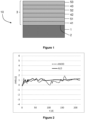
- the surface 2 of a base 1 (or a substrate) of a watch component 10 (shown in FIG. figure 1 ), in particular, according to the invention the surface of a base of a spiral spring is treated.
- the base of the watch component can be made of NbZr alloy.
- a first layer 41 of a first oxide is deposited, for example the oxide Al 2 O 3
- a second layer 51 of a second oxide is deposited, for example the oxide TiO 2 .
- phases are repeated successively, in particular 2 or 3 or 4 phases, each including the first step and the second
- a multilayer coating 3 or a coating composed of several alternating layers 41, 51, 42, 52, 43, 53 of the oxides Al 2 O 3 and TiO 2 is obtained.
- This coating is shown in figure 1 .
- this coating completely covers the surface of the watch component.
- This coating also has the particularity of being perceived as a deep blue color.
- ALD Advanced Layer Deposition
- One or more springs 1 to be treated are arranged on metal supports (for example stainless steel or aluminum) or on plastic supports resistant to the temperature required for deposition (maximum 200 ° C) and suitable for working under vacuum.
- plastic supports are for example made of PEEK (polyetheretherketone) or PPS (Polyphenylene sulphide). The supports that hold the balance spring or balance springs are then placed inside an ALD reactor.
- the hairspring or hairsprings are alternately exposed to chemical precursors.
- the deposition is preferably carried out under a continuous flow of nitrogen N 2 , for example approximately 20 sccm (standard cubic centimeter per minute) and/or for example under a pressure of approximately 20 Pa.
- N 2 nitrogen
- the substrate i.e. in particular the hairsprings
- TMA trimethylaluminium
- H 2 O water
- the spirals are exposed sequentially or alternately to Tetrakis(dimethylamido)titanium (TDMAT) and water (H 2 O) vapors to form (by successive partial layers) a layer of TiO 2 oxide with a deposition rate of 0.045 nm per exposure cycle.
- TDMAT Tetrakis(dimethylamido)titanium
- H 2 O water
- the base pressure in the chamber, reached when no precursor or gas flow is present, may depend on the characteristics of the vacuum chamber and pumps and may, for example, be less than or equal to 0.1 Torr ( ⁇ 20 Pa), preferably less than 0.01 Torr ( ⁇ 2 Pa).
- the pressure in the chamber reached under nitrogen flow is typically 20 Pa, with a working window between 10 Pa and 50 Pa.
- the pressure may depend on the deposition chamber, the nature and the surface of the components to be coated.
- Deposits such as those shown in the figure 1 were carried out at 100, 120, 140, 200 and 280°C. From a walking stability point of view, deposits made between 100°C and 280°C are satisfactory, because they allow adequate stabilization of the walking.
- the temperature of 280°C is high: it presents a risk of degradation of the chemical precursors used. A deposition temperature between 100°C and 200°C therefore seems to constitute a good compromise.
- an ALD (Atomic Layer Deposition) deposition technology is used to deposit the first and second layers, i.e. a specific thin-film deposition technique that makes it possible to obtain layers and multilayers of nanometric thickness on a wide variety of substrates.
- a deposition chamber or ALD reactor makes it possible to achieve a base pressure of less than 20 Pa, more preferably less than 2 Pa (with the units generally used by those skilled in the art, the pressure is preferably less than or equal to 0.01 Torr).
- a deposition "cycle” thus involves the introduction of a first precursor into the chamber in gaseous form for a given time, at a given flow rate (generally controlled by the duration of gas introduction or duration of the "pulse” and by the vapor pressure of the gas, itself controlled by the temperature).
- this first precursor is for example TMA (trimethylaluminum), carried by a carrier gas which is generally dinitrogen.
- TMA trimethylaluminum
- a small part of the first precursor is deposited on the surface of the substrate (and the walls of the chamber) and reacts chemically with the -OH - endings present on the surface to be coated, while the balance is evacuated by vacuum pumps.
- a second precursor is then introduced, for example water in the form of water vapor, which will react with the first precursor adsorbed on the surface to form alumina.
- the thickness of the layer formed during a deposition cycle will depend on the material deposited, and is typically 0.11 nm for Al 2 O 3 . The cycles are then repeated until the desired layer thickness is obtained for the given material.
- Multilayers are made by modifying the nature of the precursors, and in particular the nature of the first precursor.
- TDMAT Tetrakis(dimethylamido)titanium
- water water
- TiO 2 is thus obtained at a rate of typically 0.044 nm per cycle.
- other precursors it is possible to obtain other oxides such as ZrO 2 , HfO 2 or ZnO for example.
- An oxide layer for example a native oxide layer, generally has -OH terminations on the surface that facilitate deposition.
- the surface can be oxidized before deposition or the order of introduction of the precursors can be reversed.
- the doses of precursors introduced into the chamber depend on the characteristics of the deposition chamber, the nature and the surface of the parts to be coated.
- the pressure reached under nitrogen flow, which can be continuous or not, is typically 20 Pa, with a working window generally located between 10 and 50 Pa, and will also depend on the deposition chamber.
- the ALD deposition process thus makes it possible to deposit ceramic layers (oxides, nitrides and carbides) of very low thickness, extremely uniform and perfectly controlled at the subnanometric scale. This makes it possible to coat three-dimensional surfaces that are irregular and very complex from a geometric point of view that would be difficult to coat using other thin-film deposition technologies.
- a spiral spring had a coating obtained by layers made by deposits using ALD technology also on the parts of the spiral in contact with the support. Furthermore, the quality (uniformity of thickness and color) on these parts does not differ from that of the parts of the spiral directly exposed. This has the effect of greatly facilitating the production of the supports and the implementation of the treatment process, and to minimize the handling to be carried out on the components to be treated or coated. If this were not the case, it would have been necessary to avoid any contact between the surfaces to be coated and the support. The constraints of implementing the process would therefore have been significantly greater.
- FIG. 2 illustrates the changes in the average rate of watch movements over time, for two batches of movements. Both batches of movements are equipped with NbZr alloy hairsprings.
- a first batch has anodized hairsprings, for example treated using the process in the document EP1039352 .
- the evolutions of the rate of these movements are represented by a curve referenced "ANOD”.
- a second batch presents hairsprings treated according to the first method of execution of the treatment process.
- the evolutions of the rate of these movements are represented by a curve referenced "ALD”.
- a slight drift is observed during the first days of operation, of less than 1 second per day.
- the rate is then completely stable over time over the duration of the test.
- the results obtained with hairsprings treated according to the invention are entirely comparable to those obtained with hairsprings treated by anodization according to the document EP1039352 .
- the first layer and/or the second layer may have a nanometric thickness, i.e. a thickness of a few nanometers, for example less than 100 nm, in particular less than 60 nm, more particularly less than 20 nm.
- the thickness of the first layer is between 2 nm and 15 nm, preferably between 3 nm and 12 nm and/or the thickness of the second layer is between 2 nm and 15 nm, preferably between 3 nm and 12 nm.
- the total thickness of the coating 3 is preferably chosen between 10 and 300 nm, more preferably chosen between 10 nm and 150 nm, even more preferably between 10 nm and 80 nm, in order to be able to guarantee the efficiency of the deposition and not to degrade the properties of the component and/or the deposit.
- the maximum thickness is set to minimize the risk of coating cracking due to residual stresses created at the substrate-coating interface during deposition. This is important for components such as watch hairsprings that are subjected to mechanical stress in tension/compression or bending. In addition, the thinner the coating deposited, the less the mechanical properties of the hairsprings are modified.
- the thickness of the oxide layer is relatively unimportant in achieving good operating stability, so that this thickness can also be chosen according to the desired colour.
- this thickness can also be chosen according to the desired colour.
- FIG 3 illustrates the range of colours that can be obtained by selecting a first thickness of the first layers of Al 2 O 3 oxide and a second thickness of the second layers of TiO 2 oxide, in the case of the implementation of the method for producing a coating including the superposition of 6 alternating layers of oxides on a watch component comprising a base or a substrate made of NbZr alloy. All the layers of Al 2 O 3 have the same thickness ⁇ (Al 2 O 3 ). All the layers of TiO 2 have the same thickness ⁇ (TiO 2 ).
- FIG 4 illustrates the range of colors that can be obtained by selecting the same thickness for the first layers of oxide Al 2 O 3 and for the second layers of TiO 2 oxide, in the case of the implementation of the method for producing a coating including the superposition of 6 alternating layers of oxides on a watch component comprising a base or a substrate made of NbZr alloy. All the layers of Al 2 O 3 and all the layers of TiO 2 have the same thickness ⁇ .
- the thickness of the different layers can also be varied from one layer to another and from one material to another, without any technical effect discernible a priori (apart from the apparent color of the coating). If one wishes to obtain a blue-colored coating of the type comprising n double layers (Al 2 O 3
- TiO 2 ) with n between 3 and 5, an optimization leads to solutions close to those exposed above with n 3 and a thickness of each layer of 11 nm. One can also reduce the thickness of each layer to 8.5 nm or 9 nm and remain in a close color as can be seen in the figure 4 .
- the formation of the coating modifies the elastic properties of the hairspring, by reducing the apparent elastic thermal coefficient of the hairspring (by approximately 5ppm/°C for hairsprings referenced "ALD" at the figure 2 , which corresponds to a decrease in the thermal coefficient of the spiral balance oscillator of approximately 0.2 s/d/°C) and by increasing the torque. It is therefore necessary to take these differences into account when calculating the shape of the spiral and the various treatments carried out during the manufacture of the spiral, so as to obtain the elastic thermal coefficient and the torque sought after the deposition of the coating by implementing the method which is the subject of the invention.
- FIG 5 illustrates the range of colours that can be obtained by selecting a first thickness of the first layers of Al 2 O 3 oxide and a second thickness of the second layers of ZrO 2 oxide, in the case of the implementation of the method for producing a coating including the superposition of 6 alternating layers of oxides on a watch component comprising a base or a substrate made of NbZr alloy. All the layers of Al 2 O 3 have the same thickness ⁇ (Al 2 O 3 ). All the layers of ZrO 2 have the same thickness ⁇ (ZrO 2 ).
- paramagnetic alloys with suitable properties for producing watch hairsprings, in particular self-compensating hairsprings, i.e. with an adequate value of the elastic thermal coefficient. Mention is thus made of the paramagnetic alloy Nb-Zr containing between 5% and 25% by weight of Zr and at least 500 ppm by weight of a doping agent formed at least in part of oxygen; or paramagnetic alloys based on Nb, Ta, V; or alloys based on at least one element of the group Nb, V, Ta and one element of the group Ti, Zr, Hf, such as for example Nb-Hf alloys with low proportions of Hf (in particular between 2 and 4% at).
- the method is therefore applied to a substrate made of NbZr type alloy or of an alloy based on Nb or Ta or V or of an alloy based on at least one element of the group Nb, V, Ta and one element of the group Ti, Zr, Hf, such as for example Nb-Hf alloys with low proportions of Hf (in particular between 2 and 4% at).
- Ferromagnetic alloys based on iron, nickel or cobalt are frequently used for the manufacture of hairsprings (e.g. "Nivarox" alloys of the FeNiCr type).
- Deposition tests have been carried out on such hairsprings: the deposition and the resulting running stability are quite satisfactory with a 6-layer coating structure of the [(Al 2 O 3
- the resulting color of the layer was a pale blue in this case, and can be optimized if desired as shown in figure 6 .
- FIG. 6 illustrates the range of colours that can be obtained by selecting a first thickness of the first layers of Al 2 O 3 oxide and a second thickness of the second layers of TiO 2 oxide, in the case of the implementation of the process making it possible to produce a coating including the superposition of 6 alternating layers of oxides on a component watchmaker comprising a base or substrate made of FeNiCr alloy.
- All the layers of Al 2 O 3 have the same thickness ⁇ (Al 2 O 3 ).
- All the layers of TiO 2 have the same thickness ⁇ (TiO 2 ).
- the process is therefore applied to a substrate made of FeNiCr type alloy.
- the patent EP1422436 describes the production of silicon Si watch hairsprings with a deposit of silicon oxide SiO 2 on the periphery to achieve thermal compensation.
- the SiO 2 oxide layer covering the silicon can have a thickness of approximately 3 ⁇ m.
- TiO 2 ) n also makes it possible to obtain good stability of the rate over time.
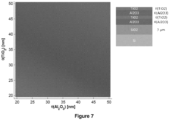
- the color can also be adjusted with the thickness and materials of the layers as illustrated in figure 7 .
- FIG 7 illustrates the range of colors that can be obtained by selecting a first thickness of the first layers of Al 2 O 3 oxide and a second thickness of the second layers of TiO 2 oxide, in the case of the implementation of the method for producing a coating including the superposition of 4 alternating layers of oxides on a watch component comprising a base or a substrate made of Si coated with a layer of silicon oxide.
- All the layers of Al 2 O 3 have the same thickness ⁇ (Al 2 O 3 ).
- All the layers of TiO 2 have the same thickness ⁇ (TiO 2 ). Satisfactory layers have thus been obtained with alternating layers of 45 nm of Al 2 O 3 and 50 nm of TiO 2 .
- the process is therefore applied to a silicon substrate or silicon substrate coated with a silicon oxide.
- the different oxide layers may have different thicknesses, in particular the different oxide layers of the same nature may have different thicknesses.
- hairspring means the hairspring alone or the hairspring and its flange and/or its ferrule.
- the invention also relates to a watch spiral spring, obtained by the method.
- the invention therefore relates to such a component itself, as defined in claim 6.
- the component comprises a base 10 and a coating 3 including a first layer 4 of a first oxide and a second layer 51 of a second oxide.
- the first layer and/or the second layer may have a nanometric thickness, i.e. a thickness of less than 100 nm.
- the first layer and/or the second layer can be deposited by an ALD deposit type procedure.
- the first oxide can be ZrO 2 or TiO 2 or HfO 2 or ZnO or preferably Al 2 O 3 . Other oxides can also be used.
- the second oxide may be different from the first oxide and may be Al 2 O 3 or ZrO 2 or HfO 2 or ZnO or preferably TiO 2 .
- the base of the watch component may be made of an alloy of the NbZr type or of silicon or of silicon coated with SiO 2 or of an alloy of the FeNiCr type.
- the base of the watch component is however not limited to these materials, but may also be made of other suitable materials, such as diamond or quartz.
- the base of the watch component can be made of an alloy based on Nb, Ta or V.
- the coating comprises several superpositions, in particular 2 or 3 or 4 superpositions, each including a first layer and a second layer.
- the layers can each completely cover the base of the watch component.
- the first and second layers are of different chemical natures.
- the first oxide, and/or the second oxide, and/or the combination of the first oxide and the second oxide in the form of a first layer and a second layer advantageously have a negative thermoelastic coefficient.
- the base on the one hand and at least one of the layers on the other hand have thermoelastic coefficients of opposite signs.
- NbZr hairsprings with layers according to the invention show a lower thermoelastic coefficient than that of hairsprings from the same production batch without an additional layer (thermal coefficient difference of the hairspring balance oscillator of -0.2 s/d/°C).
- thermoelastic coefficient of Si/SiO2 hairsprings with layers according to the invention is very significantly lower than that of hairsprings from the same production batch without an additional layer (thermal coefficient difference of the hairspring balance oscillator of -0.9 s/d/°C). In both cases, this implies that the thermoelastic coefficient of the first and/or second oxide is strongly negative, of the same sign as that of silicon for example.
- thermoelastic coefficient can be estimated at approximately -500 ppm/°C. It is therefore necessary to take into account the materials and thicknesses of the different layers when calculating the shape of the hairspring and the various treatments carried out during the manufacture of the hairspring, in order to obtain an elastic thermal coefficient and a hairspring torque suitable for the production of a balance-hairspring oscillator or resonator with the right frequency and thermocompensation properties.
- the first layer 41 is made of a first nitride and/or the second layer 51 is made of a second nitride. It follows that the first and second layers can be oxides or nitrides or respectively an oxide and a nitride or respectively a nitride and an oxide.
- the first nitride can be AlTiCN or AIN or TiN, but other nitrides can also be used.
- the second nitride is different from the first nitride and can be AlTiCN or AIN or TiN.
- the first or second carbide can be for example AlTiCN.
- the invention also relates to a movement comprising a watch component as defined above.
- the invention also relates to a timepiece, in particular a watch, comprising a movement as defined above or a watch component as defined above.
Landscapes
- Chemical & Material Sciences (AREA)
- Engineering & Computer Science (AREA)
- Mechanical Engineering (AREA)
- Chemical Kinetics & Catalysis (AREA)
- General Chemical & Material Sciences (AREA)
- Materials Engineering (AREA)
- Metallurgy (AREA)
- Organic Chemistry (AREA)
- Inorganic Chemistry (AREA)
- Manufacturing & Machinery (AREA)
- Physics & Mathematics (AREA)
- General Physics & Mathematics (AREA)
- Physical Vapour Deposition (AREA)
- Other Surface Treatments For Metallic Materials (AREA)
- Springs (AREA)
Priority Applications (2)
| Application Number | Priority Date | Filing Date | Title |
|---|---|---|---|
| EP24194470.1A EP4439193A3 (fr) | 2012-07-06 | 2013-07-08 | Procédé de traitement d'une surface d'un composant horloger et composant horloger obtenu par un tel procédé |
| EP13734432.1A EP2870512B1 (fr) | 2012-07-06 | 2013-07-08 | Procédé de traitement d'une surface d'un ressort spiral horloger et ressort spiral obtenu par un tel procédé |
Applications Claiming Priority (3)
| Application Number | Priority Date | Filing Date | Title |
|---|---|---|---|
| EP12175240 | 2012-07-06 | ||
| EP13734432.1A EP2870512B1 (fr) | 2012-07-06 | 2013-07-08 | Procédé de traitement d'une surface d'un ressort spiral horloger et ressort spiral obtenu par un tel procédé |
| PCT/EP2013/064413 WO2014006229A1 (fr) | 2012-07-06 | 2013-07-08 | Procédé de traitement d'une surface d'un composant horloger et composant horloger obtenu par un tel procédé |
Related Child Applications (1)
| Application Number | Title | Priority Date | Filing Date |
|---|---|---|---|
| EP24194470.1A Division EP4439193A3 (fr) | 2012-07-06 | 2013-07-08 | Procédé de traitement d'une surface d'un composant horloger et composant horloger obtenu par un tel procédé |
Publications (2)
| Publication Number | Publication Date |
|---|---|
| EP2870512A1 EP2870512A1 (fr) | 2015-05-13 |
| EP2870512B1 true EP2870512B1 (fr) | 2024-09-11 |
Family
ID=48747586
Family Applications (2)
| Application Number | Title | Priority Date | Filing Date |
|---|---|---|---|
| EP13734432.1A Active EP2870512B1 (fr) | 2012-07-06 | 2013-07-08 | Procédé de traitement d'une surface d'un ressort spiral horloger et ressort spiral obtenu par un tel procédé |
| EP24194470.1A Pending EP4439193A3 (fr) | 2012-07-06 | 2013-07-08 | Procédé de traitement d'une surface d'un composant horloger et composant horloger obtenu par un tel procédé |
Family Applications After (1)
| Application Number | Title | Priority Date | Filing Date |
|---|---|---|---|
| EP24194470.1A Pending EP4439193A3 (fr) | 2012-07-06 | 2013-07-08 | Procédé de traitement d'une surface d'un composant horloger et composant horloger obtenu par un tel procédé |
Country Status (5)
| Country | Link |
|---|---|
| US (2) | US10372083B2 (enExample) |
| EP (2) | EP2870512B1 (enExample) |
| JP (2) | JP6407146B2 (enExample) |
| CN (1) | CN104583880B (enExample) |
| WO (1) | WO2014006229A1 (enExample) |
Families Citing this family (18)
| Publication number | Priority date | Publication date | Assignee | Title |
|---|---|---|---|---|
| EP3002638B1 (fr) * | 2014-09-08 | 2021-08-18 | Richemont International S.A. | Procédé de fabrication d'un ressort spiral thermocompensé |
| CH711218B1 (fr) * | 2015-06-16 | 2019-06-14 | Nivarox Sa | Procédé de fabrication d'un composant horloger. |
| EP3106928A1 (fr) * | 2015-06-16 | 2016-12-21 | Nivarox-FAR S.A. | Procédé de fabrication comportant une étape de décolletage modifiée |
| US20170285573A1 (en) * | 2016-11-30 | 2017-10-05 | Firehouse Horology, Inc. | Crystalline Compounds for Use in Mechanical Watches and Methods of Manufacture Thereof |
| EP3422116B1 (fr) * | 2017-06-26 | 2020-11-04 | Nivarox-FAR S.A. | Ressort spiral d'horlogerie |
| EP3456859A1 (en) * | 2017-09-13 | 2019-03-20 | Rolex Sa | Protective coating for a complex watch component |
| EP3608728B1 (fr) | 2018-08-08 | 2022-02-16 | Nivarox-FAR S.A. | Spiral thermocompensé coloré et son procédé de fabrication |
| JP6908064B2 (ja) * | 2019-03-14 | 2021-07-21 | セイコーエプソン株式会社 | 時計用部品、時計用ムーブメントおよび時計 |
| EP3736638B1 (fr) * | 2019-05-07 | 2021-12-01 | Nivarox-FAR S.A. | Procede de fabrication d'un ressort spiral pour mouvement d'horlogerie |
| EP3736639B1 (fr) * | 2019-05-07 | 2024-07-03 | Nivarox-FAR S.A. | Procede de fabrication d'un ressort spiral pour mouvement d'horlogerie |
| EP3798739B1 (fr) * | 2019-09-24 | 2025-07-02 | Rolex Sa | Composant horloger |
| EP3839644B1 (fr) * | 2019-12-20 | 2026-01-28 | Nivarox-FAR S.A. | Composant horloger flexible, notamment pour mecanisme oscillateur, et mouvement d'horlogerie comportant un tel composant |
| EP3954802A1 (fr) * | 2020-08-11 | 2022-02-16 | Omega SA | Composant noir decore de pierres et son procede de fabrication |
| EP3968097B1 (fr) * | 2020-09-09 | 2025-03-26 | Nivarox-FAR S.A. | Ensemble horloger et son procédé de fabrication |
| EP4001458B1 (fr) * | 2020-11-17 | 2024-10-16 | The Swatch Group Research and Development Ltd | Procede de depot d'un revetement sur un composant horloger et composant horloger revetu par un tel procede |
| US12493265B2 (en) * | 2022-03-14 | 2025-12-09 | Seiko Watch Kabushiki Kaisha (trading as Seiko Watch Corporation) | Hairspring, timepiece movement, and timepiece |
| EP4520717A1 (fr) * | 2023-09-05 | 2025-03-12 | Patek Philippe SA Genève | Procédé de fabrication d'un composant horloger en matériau sans déformation plastique, notamment en silicium |
| EP4759963A1 (fr) | 2024-12-16 | 2026-06-17 | Richemont International Sa | Composant horloger avec couche fonctionnelle |
Citations (1)
| Publication number | Priority date | Publication date | Assignee | Title |
|---|---|---|---|---|
| US20030224201A1 (en) * | 2002-01-16 | 2003-12-04 | Atsushi Kawakami | Surface processing method for decorative articles, a decorative article, and a timepiece |
Family Cites Families (15)
| Publication number | Priority date | Publication date | Assignee | Title |
|---|---|---|---|---|
| DE69710445T2 (de) | 1997-06-20 | 2002-10-10 | Manufacture Des Montres Rolex S.A., Biel/Bienne | Selbstkompensierende Spiralfeder für mechanische Uhrwerkunruhspiralfederoszillator und Verfahren zu deren Herstellung |
| DE69911913T2 (de) | 1999-03-26 | 2004-09-09 | Rolex Sa | Selbstkompensierende Spiralfeder für Uhrwerkspiralfederunruh und Verfahren zur Behandlung derselben |
| DE1258786T1 (de) | 2001-05-18 | 2003-08-14 | Rolex S.A., Genf/Geneve | Selbstkompensierende Feder für einen mechanischen Oszillator vom Unruh-Spiralfeder-Typ |
| JP3960227B2 (ja) * | 2002-01-16 | 2007-08-15 | セイコーエプソン株式会社 | 装飾品の表面処理方法、装飾品および時計 |
| ATE307990T1 (de) | 2002-11-25 | 2005-11-15 | Suisse Electronique Microtech | Spiraluhrwerkfeder und verfahren zu deren herstellung |
| JP4073848B2 (ja) * | 2003-09-01 | 2008-04-09 | シチズンホールディングス株式会社 | 装飾品およびその製造方法 |
| JP5328577B2 (ja) * | 2008-09-08 | 2013-10-30 | シチズン時計株式会社 | 装飾品およびその製造方法 |
| DE202010018420U1 (de) * | 2009-02-06 | 2016-06-22 | Damasko Gmbh | Mechanisches Schwingsystem für eine Uhr und Unruhfeder für eine Uhr |
| EP2273324A1 (fr) | 2009-07-06 | 2011-01-12 | ETA SA Manufacture Horlogère Suisse | Procédé de fabrication d'une pièce en relief décorée |
| CH702353A2 (fr) | 2009-12-15 | 2011-06-15 | Swatch Group Res & Dev Ltd | Résonateur thermocompensé au moins aux premier et second ordres. |
| EP2337221A1 (fr) * | 2009-12-15 | 2011-06-22 | The Swatch Group Research and Development Ltd. | Résonateur thermocompensé au moins aux premier et second ordres |
| US20120314546A1 (en) | 2010-02-17 | 2012-12-13 | Brewer Donald R | Timepiece with twist restricted flexible display |
| US20110236654A1 (en) | 2010-03-26 | 2011-09-29 | Wen-Kuang Hsu | Method of surface treatment and surface treated article provied by the same |
| CN102947764B (zh) * | 2010-06-23 | 2015-09-16 | 西铁城控股株式会社 | 钟表用显示板 |
| EP2597536A1 (fr) * | 2011-11-25 | 2013-05-29 | CSEM Centre Suisse d'Electronique et de Microtechnique SA - Recherche et Développement | Ressort spiral amélioré et procédé de fabrication dudit ressort spiral |
-
2013
- 2013-07-08 WO PCT/EP2013/064413 patent/WO2014006229A1/fr not_active Ceased
- 2013-07-08 US US14/412,845 patent/US10372083B2/en active Active
- 2013-07-08 EP EP13734432.1A patent/EP2870512B1/fr active Active
- 2013-07-08 CN CN201380036217.1A patent/CN104583880B/zh active Active
- 2013-07-08 JP JP2015519249A patent/JP6407146B2/ja active Active
- 2013-07-08 EP EP24194470.1A patent/EP4439193A3/fr active Pending
-
2018
- 2018-07-12 JP JP2018131997A patent/JP6550176B2/ja active Active
-
2019
- 2019-05-21 US US16/418,023 patent/US11914328B2/en active Active
Patent Citations (1)
| Publication number | Priority date | Publication date | Assignee | Title |
|---|---|---|---|---|
| US20030224201A1 (en) * | 2002-01-16 | 2003-12-04 | Atsushi Kawakami | Surface processing method for decorative articles, a decorative article, and a timepiece |
Also Published As
| Publication number | Publication date |
|---|---|
| JP2018173425A (ja) | 2018-11-08 |
| EP4439193A2 (fr) | 2024-10-02 |
| CN104583880B (zh) | 2018-07-13 |
| JP6407146B2 (ja) | 2018-10-17 |
| EP4439193A3 (fr) | 2024-12-18 |
| EP2870512A1 (fr) | 2015-05-13 |
| JP2015522152A (ja) | 2015-08-03 |
| US11914328B2 (en) | 2024-02-27 |
| CN104583880A (zh) | 2015-04-29 |
| US10372083B2 (en) | 2019-08-06 |
| US20190271947A1 (en) | 2019-09-05 |
| WO2014006229A1 (fr) | 2014-01-09 |
| JP6550176B2 (ja) | 2019-07-24 |
| US20150185701A1 (en) | 2015-07-02 |
Similar Documents
| Publication | Publication Date | Title |
|---|---|---|
| EP4439193A2 (fr) | Procédé de traitement d'une surface d'un composant horloger et composant horloger obtenu par un tel procédé | |
| CN108126681B (zh) | 用于增强二氧化钛(TiO2)涂层的光催化活性的成核层 | |
| RU2660878C2 (ru) | Алмазное покрытие и способ его осаждения | |
| EP3502785B1 (fr) | Ressort spiral pour mouvement d'horlogerie et son procédé de fabrication | |
| EP2392689A1 (fr) | Article décoratif avec revêtement rouge et procédé | |
| EP3592879A1 (fr) | Materiau comprenant une couche mince d'un alliage comportant du titane et de l'or et procede d'obtention d'un tel materiau | |
| WO2015140261A1 (fr) | Procédé de dépôt en phase gazeuse | |
| CH714139A2 (fr) | Revêtement protecteur pour composant horloger complexe. | |
| EP1636399A1 (fr) | Revetement pour une piece mecanique comprenant au moins une couche externe de carbone amorphe hydrogene et une couche de carbure de silicium hydrogene en contact avec la piece, et procede de depot d'un tel revetement | |
| TWI688113B (zh) | 用於光學元件增強之濕潤層 | |
| CH714492A2 (fr) | Ressort spiral pour mouvement d'horlogerie et son procédé de fabrication. | |
| Kim et al. | Uniform color coating of multilayered TiO2/Al2O3 films by atomic layer deposition | |
| CH708413B1 (fr) | Substrat comprenant un revêtement de diamant et procédé de dépôt d'un tel revêtement. | |
| WO2025068217A1 (fr) | Composant de rappel élastique pour mouvement horloger | |
| WO2009083673A1 (fr) | Procede de realisation de revetement en carbone amorphe hydrogene | |
| FR3059340B1 (fr) | Procede de depot de couche de chalcogenure sur un substrat | |
| CH714491A2 (fr) | Ressort spiral pour mouvement d'horlogerie et son procédé de fabrication. | |
| CH711501A2 (fr) | Procédé de fabrication d'une pièce micromécanique horlogère et ladite pièce micromécanique horlogère. | |
| EP4726478A1 (fr) | Revêtement mince de décoration à teinte noir en tialc | |
| CN117604489A (zh) | 一种低频率漂移率铷原子钟的复合薄膜结构及其制备方法 | |
| EP4485088A1 (fr) | Procédé de retrait d'un matériau céramique | |
| CH718082A2 (fr) | Procédé de fabrication d'un élément élastique pour un système micromécanique. | |
| CH719817B1 (fr) | Article irisé et son procédé de fabrication | |
| WO2021255286A1 (fr) | Procédé de réalisation d'une couche sur certaines surfaces seulement d'une structure | |
| CH720939A1 (fr) | Procédé de fabrication d'un composant horloger comportant une couche métallique de décoration revêtue par une couche de protection céramique transparente |
Legal Events
| Date | Code | Title | Description |
|---|---|---|---|
| PUAI | Public reference made under article 153(3) epc to a published international application that has entered the european phase |
Free format text: ORIGINAL CODE: 0009012 |
|
| 17P | Request for examination filed |
Effective date: 20150112 |
|
| AK | Designated contracting states |
Kind code of ref document: A1 Designated state(s): AL AT BE BG CH CY CZ DE DK EE ES FI FR GB GR HR HU IE IS IT LI LT LU LV MC MK MT NL NO PL PT RO RS SE SI SK SM TR |
|
| AX | Request for extension of the european patent |
Extension state: BA ME |
|
| DAX | Request for extension of the european patent (deleted) | ||
| STAA | Information on the status of an ep patent application or granted ep patent |
Free format text: STATUS: EXAMINATION IS IN PROGRESS |
|
| 17Q | First examination report despatched |
Effective date: 20200724 |
|
| P01 | Opt-out of the competence of the unified patent court (upc) registered |
Effective date: 20230530 |
|
| GRAP | Despatch of communication of intention to grant a patent |
Free format text: ORIGINAL CODE: EPIDOSNIGR1 |
|
| STAA | Information on the status of an ep patent application or granted ep patent |
Free format text: STATUS: GRANT OF PATENT IS INTENDED |
|
| INTG | Intention to grant announced |
Effective date: 20240405 |
|
| RIN1 | Information on inventor provided before grant (corrected) |
Inventor name: TOBENAS BORRON, SUSANA DEL CARMEN |
|
| GRAS | Grant fee paid |
Free format text: ORIGINAL CODE: EPIDOSNIGR3 |
|
| GRAA | (expected) grant |
Free format text: ORIGINAL CODE: 0009210 |
|
| STAA | Information on the status of an ep patent application or granted ep patent |
Free format text: STATUS: THE PATENT HAS BEEN GRANTED |
|
| AK | Designated contracting states |
Kind code of ref document: B1 Designated state(s): AL AT BE BG CH CY CZ DE DK EE ES FI FR GB GR HR HU IE IS IT LI LT LU LV MC MK MT NL NO PL PT RO RS SE SI SK SM TR |
|
| REG | Reference to a national code |
Ref country code: GB Ref legal event code: FG4D Free format text: NOT ENGLISH |
|
| REG | Reference to a national code |
Ref country code: CH Ref legal event code: EP |
|
| REG | Reference to a national code |
Ref country code: DE Ref legal event code: R096 Ref document number: 602013086075 Country of ref document: DE |
|
| REG | Reference to a national code |
Ref country code: IE Ref legal event code: FG4D Free format text: LANGUAGE OF EP DOCUMENT: FRENCH |
|
| REG | Reference to a national code |
Ref country code: LT Ref legal event code: MG9D |
|
| PG25 | Lapsed in a contracting state [announced via postgrant information from national office to epo] |
Ref country code: NO Free format text: LAPSE BECAUSE OF FAILURE TO SUBMIT A TRANSLATION OF THE DESCRIPTION OR TO PAY THE FEE WITHIN THE PRESCRIBED TIME-LIMIT Effective date: 20241211 |
|
| REG | Reference to a national code |
Ref country code: NL Ref legal event code: MP Effective date: 20240911 |
|
| PG25 | Lapsed in a contracting state [announced via postgrant information from national office to epo] |
Ref country code: GR Free format text: LAPSE BECAUSE OF FAILURE TO SUBMIT A TRANSLATION OF THE DESCRIPTION OR TO PAY THE FEE WITHIN THE PRESCRIBED TIME-LIMIT Effective date: 20241212 Ref country code: FI Free format text: LAPSE BECAUSE OF FAILURE TO SUBMIT A TRANSLATION OF THE DESCRIPTION OR TO PAY THE FEE WITHIN THE PRESCRIBED TIME-LIMIT Effective date: 20240911 |
|
| PG25 | Lapsed in a contracting state [announced via postgrant information from national office to epo] |
Ref country code: BG Free format text: LAPSE BECAUSE OF FAILURE TO SUBMIT A TRANSLATION OF THE DESCRIPTION OR TO PAY THE FEE WITHIN THE PRESCRIBED TIME-LIMIT Effective date: 20240911 |
|
| PG25 | Lapsed in a contracting state [announced via postgrant information from national office to epo] |
Ref country code: LV Free format text: LAPSE BECAUSE OF FAILURE TO SUBMIT A TRANSLATION OF THE DESCRIPTION OR TO PAY THE FEE WITHIN THE PRESCRIBED TIME-LIMIT Effective date: 20240911 |
|
| PG25 | Lapsed in a contracting state [announced via postgrant information from national office to epo] |
Ref country code: HR Free format text: LAPSE BECAUSE OF FAILURE TO SUBMIT A TRANSLATION OF THE DESCRIPTION OR TO PAY THE FEE WITHIN THE PRESCRIBED TIME-LIMIT Effective date: 20240911 |
|
| PG25 | Lapsed in a contracting state [announced via postgrant information from national office to epo] |
Ref country code: ES Free format text: LAPSE BECAUSE OF FAILURE TO SUBMIT A TRANSLATION OF THE DESCRIPTION OR TO PAY THE FEE WITHIN THE PRESCRIBED TIME-LIMIT Effective date: 20240911 Ref country code: RS Free format text: LAPSE BECAUSE OF FAILURE TO SUBMIT A TRANSLATION OF THE DESCRIPTION OR TO PAY THE FEE WITHIN THE PRESCRIBED TIME-LIMIT Effective date: 20241211 |
|
| PG25 | Lapsed in a contracting state [announced via postgrant information from national office to epo] |
Ref country code: RS Free format text: LAPSE BECAUSE OF FAILURE TO SUBMIT A TRANSLATION OF THE DESCRIPTION OR TO PAY THE FEE WITHIN THE PRESCRIBED TIME-LIMIT Effective date: 20241211 Ref country code: NO Free format text: LAPSE BECAUSE OF FAILURE TO SUBMIT A TRANSLATION OF THE DESCRIPTION OR TO PAY THE FEE WITHIN THE PRESCRIBED TIME-LIMIT Effective date: 20241211 Ref country code: LV Free format text: LAPSE BECAUSE OF FAILURE TO SUBMIT A TRANSLATION OF THE DESCRIPTION OR TO PAY THE FEE WITHIN THE PRESCRIBED TIME-LIMIT Effective date: 20240911 Ref country code: HR Free format text: LAPSE BECAUSE OF FAILURE TO SUBMIT A TRANSLATION OF THE DESCRIPTION OR TO PAY THE FEE WITHIN THE PRESCRIBED TIME-LIMIT Effective date: 20240911 Ref country code: GR Free format text: LAPSE BECAUSE OF FAILURE TO SUBMIT A TRANSLATION OF THE DESCRIPTION OR TO PAY THE FEE WITHIN THE PRESCRIBED TIME-LIMIT Effective date: 20241212 Ref country code: FI Free format text: LAPSE BECAUSE OF FAILURE TO SUBMIT A TRANSLATION OF THE DESCRIPTION OR TO PAY THE FEE WITHIN THE PRESCRIBED TIME-LIMIT Effective date: 20240911 Ref country code: ES Free format text: LAPSE BECAUSE OF FAILURE TO SUBMIT A TRANSLATION OF THE DESCRIPTION OR TO PAY THE FEE WITHIN THE PRESCRIBED TIME-LIMIT Effective date: 20240911 Ref country code: BG Free format text: LAPSE BECAUSE OF FAILURE TO SUBMIT A TRANSLATION OF THE DESCRIPTION OR TO PAY THE FEE WITHIN THE PRESCRIBED TIME-LIMIT Effective date: 20240911 |
|
| REG | Reference to a national code |
Ref country code: AT Ref legal event code: MK05 Ref document number: 1723218 Country of ref document: AT Kind code of ref document: T Effective date: 20240911 |
|
| PG25 | Lapsed in a contracting state [announced via postgrant information from national office to epo] |
Ref country code: NL Free format text: LAPSE BECAUSE OF FAILURE TO SUBMIT A TRANSLATION OF THE DESCRIPTION OR TO PAY THE FEE WITHIN THE PRESCRIBED TIME-LIMIT Effective date: 20240911 |
|
| PG25 | Lapsed in a contracting state [announced via postgrant information from national office to epo] |
Ref country code: IS Free format text: LAPSE BECAUSE OF FAILURE TO SUBMIT A TRANSLATION OF THE DESCRIPTION OR TO PAY THE FEE WITHIN THE PRESCRIBED TIME-LIMIT Effective date: 20250111 Ref country code: PT Free format text: LAPSE BECAUSE OF FAILURE TO SUBMIT A TRANSLATION OF THE DESCRIPTION OR TO PAY THE FEE WITHIN THE PRESCRIBED TIME-LIMIT Effective date: 20250113 |
|
| PG25 | Lapsed in a contracting state [announced via postgrant information from national office to epo] |
Ref country code: SM Free format text: LAPSE BECAUSE OF FAILURE TO SUBMIT A TRANSLATION OF THE DESCRIPTION OR TO PAY THE FEE WITHIN THE PRESCRIBED TIME-LIMIT Effective date: 20240911 Ref country code: RO Free format text: LAPSE BECAUSE OF FAILURE TO SUBMIT A TRANSLATION OF THE DESCRIPTION OR TO PAY THE FEE WITHIN THE PRESCRIBED TIME-LIMIT Effective date: 20240911 |
|
| PG25 | Lapsed in a contracting state [announced via postgrant information from national office to epo] |
Ref country code: EE Free format text: LAPSE BECAUSE OF FAILURE TO SUBMIT A TRANSLATION OF THE DESCRIPTION OR TO PAY THE FEE WITHIN THE PRESCRIBED TIME-LIMIT Effective date: 20240911 Ref country code: AT Free format text: LAPSE BECAUSE OF FAILURE TO SUBMIT A TRANSLATION OF THE DESCRIPTION OR TO PAY THE FEE WITHIN THE PRESCRIBED TIME-LIMIT Effective date: 20240911 |
|
| PG25 | Lapsed in a contracting state [announced via postgrant information from national office to epo] |
Ref country code: PL Free format text: LAPSE BECAUSE OF FAILURE TO SUBMIT A TRANSLATION OF THE DESCRIPTION OR TO PAY THE FEE WITHIN THE PRESCRIBED TIME-LIMIT Effective date: 20240911 Ref country code: CZ Free format text: LAPSE BECAUSE OF FAILURE TO SUBMIT A TRANSLATION OF THE DESCRIPTION OR TO PAY THE FEE WITHIN THE PRESCRIBED TIME-LIMIT Effective date: 20240911 |
|
| PG25 | Lapsed in a contracting state [announced via postgrant information from national office to epo] |
Ref country code: SK Free format text: LAPSE BECAUSE OF FAILURE TO SUBMIT A TRANSLATION OF THE DESCRIPTION OR TO PAY THE FEE WITHIN THE PRESCRIBED TIME-LIMIT Effective date: 20240911 Ref country code: IT Free format text: LAPSE BECAUSE OF FAILURE TO SUBMIT A TRANSLATION OF THE DESCRIPTION OR TO PAY THE FEE WITHIN THE PRESCRIBED TIME-LIMIT Effective date: 20240911 |
|
| REG | Reference to a national code |
Ref country code: DE Ref legal event code: R097 Ref document number: 602013086075 Country of ref document: DE |
|
| PG25 | Lapsed in a contracting state [announced via postgrant information from national office to epo] |
Ref country code: DK Free format text: LAPSE BECAUSE OF FAILURE TO SUBMIT A TRANSLATION OF THE DESCRIPTION OR TO PAY THE FEE WITHIN THE PRESCRIBED TIME-LIMIT Effective date: 20240911 |
|
| PLBE | No opposition filed within time limit |
Free format text: ORIGINAL CODE: 0009261 |
|
| STAA | Information on the status of an ep patent application or granted ep patent |
Free format text: STATUS: NO OPPOSITION FILED WITHIN TIME LIMIT |
|
| 26N | No opposition filed |
Effective date: 20250612 |
|
| PG25 | Lapsed in a contracting state [announced via postgrant information from national office to epo] |
Ref country code: SE Free format text: LAPSE BECAUSE OF FAILURE TO SUBMIT A TRANSLATION OF THE DESCRIPTION OR TO PAY THE FEE WITHIN THE PRESCRIBED TIME-LIMIT Effective date: 20240911 |
|
| PGFP | Annual fee paid to national office [announced via postgrant information from national office to epo] |
Ref country code: DE Payment date: 20250711 Year of fee payment: 13 |
|
| PGFP | Annual fee paid to national office [announced via postgrant information from national office to epo] |
Ref country code: GB Payment date: 20250723 Year of fee payment: 13 |
|
| PGFP | Annual fee paid to national office [announced via postgrant information from national office to epo] |
Ref country code: FR Payment date: 20250730 Year of fee payment: 13 |
|
| PGFP | Annual fee paid to national office [announced via postgrant information from national office to epo] |
Ref country code: CH Payment date: 20250801 Year of fee payment: 13 |
|
| PG25 | Lapsed in a contracting state [announced via postgrant information from national office to epo] |
Ref country code: LU Free format text: LAPSE BECAUSE OF NON-PAYMENT OF DUE FEES Effective date: 20250708 |
|
| REG | Reference to a national code |
Ref country code: BE Ref legal event code: MM Effective date: 20250731 |
|
| PG25 | Lapsed in a contracting state [announced via postgrant information from national office to epo] |
Ref country code: BE Free format text: LAPSE BECAUSE OF NON-PAYMENT OF DUE FEES Effective date: 20250731 |
|
| PG25 | Lapsed in a contracting state [announced via postgrant information from national office to epo] |
Ref country code: LT Free format text: LAPSE BECAUSE OF FAILURE TO SUBMIT A TRANSLATION OF THE DESCRIPTION OR TO PAY THE FEE WITHIN THE PRESCRIBED TIME-LIMIT Effective date: 20240911 |
|
| PG25 | Lapsed in a contracting state [announced via postgrant information from national office to epo] |
Ref country code: IE Free format text: LAPSE BECAUSE OF NON-PAYMENT OF DUE FEES Effective date: 20250708 |
|
| PG25 | Lapsed in a contracting state [announced via postgrant information from national office to epo] |
Ref country code: MC Free format text: LAPSE BECAUSE OF FAILURE TO SUBMIT A TRANSLATION OF THE DESCRIPTION OR TO PAY THE FEE WITHIN THE PRESCRIBED TIME-LIMIT Effective date: 20240911 |
|
| REG | Reference to a national code |
Ref country code: CH Ref legal event code: U11 Free format text: ST27 STATUS EVENT CODE: U-0-0-U10-U11 (AS PROVIDED BY THE NATIONAL OFFICE) Effective date: 20260801 |
|
| PG25 | Lapsed in a contracting state [announced via postgrant information from national office to epo] |
Ref country code: CY Free format text: LAPSE BECAUSE OF FAILURE TO SUBMIT A TRANSLATION OF THE DESCRIPTION OR TO PAY THE FEE WITHIN THE PRESCRIBED TIME-LIMIT Effective date: 20240911 |