EP2868776B1 - Electronic component metal material and manufacturing method thereof, and connector terminal, connector and electronic component using said electronic component metal material - Google Patents
Electronic component metal material and manufacturing method thereof, and connector terminal, connector and electronic component using said electronic component metal material Download PDFInfo
- Publication number
- EP2868776B1 EP2868776B1 EP13809664.9A EP13809664A EP2868776B1 EP 2868776 B1 EP2868776 B1 EP 2868776B1 EP 13809664 A EP13809664 A EP 13809664A EP 2868776 B1 EP2868776 B1 EP 2868776B1
- Authority
- EP
- European Patent Office
- Prior art keywords
- metallic material
- electronic components
- layer
- outermost layer
- components according
- Prior art date
- Legal status (The legal status is an assumption and is not a legal conclusion. Google has not performed a legal analysis and makes no representation as to the accuracy of the status listed.)
- Active
Links
Images


Classifications
-
- C—CHEMISTRY; METALLURGY
- C25—ELECTROLYTIC OR ELECTROPHORETIC PROCESSES; APPARATUS THEREFOR
- C25D—PROCESSES FOR THE ELECTROLYTIC OR ELECTROPHORETIC PRODUCTION OF COATINGS; ELECTROFORMING; APPARATUS THEREFOR
- C25D5/00—Electroplating characterised by the process; Pretreatment or after-treatment of workpieces
- C25D5/60—Electroplating characterised by the structure or texture of the layers
- C25D5/605—Surface topography of the layers, e.g. rough, dendritic or nodular layers
- C25D5/611—Smooth layers
-
- B—PERFORMING OPERATIONS; TRANSPORTING
- B32—LAYERED PRODUCTS
- B32B—LAYERED PRODUCTS, i.e. PRODUCTS BUILT-UP OF STRATA OF FLAT OR NON-FLAT, e.g. CELLULAR OR HONEYCOMB, FORM
- B32B15/00—Layered products comprising a layer of metal
- B32B15/01—Layered products comprising a layer of metal all layers being exclusively metallic
-
- C—CHEMISTRY; METALLURGY
- C22—METALLURGY; FERROUS OR NON-FERROUS ALLOYS; TREATMENT OF ALLOYS OR NON-FERROUS METALS
- C22C—ALLOYS
- C22C13/00—Alloys based on tin
-
- C—CHEMISTRY; METALLURGY
- C22—METALLURGY; FERROUS OR NON-FERROUS ALLOYS; TREATMENT OF ALLOYS OR NON-FERROUS METALS
- C22C—ALLOYS
- C22C5/00—Alloys based on noble metals
- C22C5/06—Alloys based on silver
-
- C—CHEMISTRY; METALLURGY
- C23—COATING METALLIC MATERIAL; COATING MATERIAL WITH METALLIC MATERIAL; CHEMICAL SURFACE TREATMENT; DIFFUSION TREATMENT OF METALLIC MATERIAL; COATING BY VACUUM EVAPORATION, BY SPUTTERING, BY ION IMPLANTATION OR BY CHEMICAL VAPOUR DEPOSITION, IN GENERAL; INHIBITING CORROSION OF METALLIC MATERIAL OR INCRUSTATION IN GENERAL
- C23C—COATING METALLIC MATERIAL; COATING MATERIAL WITH METALLIC MATERIAL; SURFACE TREATMENT OF METALLIC MATERIAL BY DIFFUSION INTO THE SURFACE, BY CHEMICAL CONVERSION OR SUBSTITUTION; COATING BY VACUUM EVAPORATION, BY SPUTTERING, BY ION IMPLANTATION OR BY CHEMICAL VAPOUR DEPOSITION, IN GENERAL
- C23C18/00—Chemical coating by decomposition of either liquid compounds or solutions of the coating forming compounds, without leaving reaction products of surface material in the coating; Contact plating
- C23C18/16—Chemical coating by decomposition of either liquid compounds or solutions of the coating forming compounds, without leaving reaction products of surface material in the coating; Contact plating by reduction or substitution, e.g. electroless plating
- C23C18/18—Pretreatment of the material to be coated
- C23C18/1851—Pretreatment of the material to be coated of surfaces of non-metallic or semiconducting in organic material
- C23C18/1872—Pretreatment of the material to be coated of surfaces of non-metallic or semiconducting in organic material by chemical pretreatment
- C23C18/1875—Pretreatment of the material to be coated of surfaces of non-metallic or semiconducting in organic material by chemical pretreatment only one step pretreatment
- C23C18/1882—Use of organic or inorganic compounds other than metals, e.g. activation, sensitisation with polymers
-
- C—CHEMISTRY; METALLURGY
- C23—COATING METALLIC MATERIAL; COATING MATERIAL WITH METALLIC MATERIAL; CHEMICAL SURFACE TREATMENT; DIFFUSION TREATMENT OF METALLIC MATERIAL; COATING BY VACUUM EVAPORATION, BY SPUTTERING, BY ION IMPLANTATION OR BY CHEMICAL VAPOUR DEPOSITION, IN GENERAL; INHIBITING CORROSION OF METALLIC MATERIAL OR INCRUSTATION IN GENERAL
- C23C—COATING METALLIC MATERIAL; COATING MATERIAL WITH METALLIC MATERIAL; SURFACE TREATMENT OF METALLIC MATERIAL BY DIFFUSION INTO THE SURFACE, BY CHEMICAL CONVERSION OR SUBSTITUTION; COATING BY VACUUM EVAPORATION, BY SPUTTERING, BY ION IMPLANTATION OR BY CHEMICAL VAPOUR DEPOSITION, IN GENERAL
- C23C28/00—Coating for obtaining at least two superposed coatings either by methods not provided for in a single one of groups C23C2/00 - C23C26/00 or by combinations of methods provided for in subclasses C23C and C25C or C25D
- C23C28/02—Coating for obtaining at least two superposed coatings either by methods not provided for in a single one of groups C23C2/00 - C23C26/00 or by combinations of methods provided for in subclasses C23C and C25C or C25D only coatings only including layers of metallic material
- C23C28/021—Coating for obtaining at least two superposed coatings either by methods not provided for in a single one of groups C23C2/00 - C23C26/00 or by combinations of methods provided for in subclasses C23C and C25C or C25D only coatings only including layers of metallic material including at least one metal alloy layer
-
- C—CHEMISTRY; METALLURGY
- C23—COATING METALLIC MATERIAL; COATING MATERIAL WITH METALLIC MATERIAL; CHEMICAL SURFACE TREATMENT; DIFFUSION TREATMENT OF METALLIC MATERIAL; COATING BY VACUUM EVAPORATION, BY SPUTTERING, BY ION IMPLANTATION OR BY CHEMICAL VAPOUR DEPOSITION, IN GENERAL; INHIBITING CORROSION OF METALLIC MATERIAL OR INCRUSTATION IN GENERAL
- C23C—COATING METALLIC MATERIAL; COATING MATERIAL WITH METALLIC MATERIAL; SURFACE TREATMENT OF METALLIC MATERIAL BY DIFFUSION INTO THE SURFACE, BY CHEMICAL CONVERSION OR SUBSTITUTION; COATING BY VACUUM EVAPORATION, BY SPUTTERING, BY ION IMPLANTATION OR BY CHEMICAL VAPOUR DEPOSITION, IN GENERAL
- C23C28/00—Coating for obtaining at least two superposed coatings either by methods not provided for in a single one of groups C23C2/00 - C23C26/00 or by combinations of methods provided for in subclasses C23C and C25C or C25D
- C23C28/30—Coatings combining at least one metallic layer and at least one inorganic non-metallic layer
- C23C28/32—Coatings combining at least one metallic layer and at least one inorganic non-metallic layer including at least one pure metallic layer
- C23C28/321—Coatings combining at least one metallic layer and at least one inorganic non-metallic layer including at least one pure metallic layer with at least one metal alloy layer
-
- C—CHEMISTRY; METALLURGY
- C23—COATING METALLIC MATERIAL; COATING MATERIAL WITH METALLIC MATERIAL; CHEMICAL SURFACE TREATMENT; DIFFUSION TREATMENT OF METALLIC MATERIAL; COATING BY VACUUM EVAPORATION, BY SPUTTERING, BY ION IMPLANTATION OR BY CHEMICAL VAPOUR DEPOSITION, IN GENERAL; INHIBITING CORROSION OF METALLIC MATERIAL OR INCRUSTATION IN GENERAL
- C23C—COATING METALLIC MATERIAL; COATING MATERIAL WITH METALLIC MATERIAL; SURFACE TREATMENT OF METALLIC MATERIAL BY DIFFUSION INTO THE SURFACE, BY CHEMICAL CONVERSION OR SUBSTITUTION; COATING BY VACUUM EVAPORATION, BY SPUTTERING, BY ION IMPLANTATION OR BY CHEMICAL VAPOUR DEPOSITION, IN GENERAL
- C23C28/00—Coating for obtaining at least two superposed coatings either by methods not provided for in a single one of groups C23C2/00 - C23C26/00 or by combinations of methods provided for in subclasses C23C and C25C or C25D
- C23C28/30—Coatings combining at least one metallic layer and at least one inorganic non-metallic layer
- C23C28/34—Coatings combining at least one metallic layer and at least one inorganic non-metallic layer including at least one inorganic non-metallic material layer, e.g. metal carbide, nitride, boride, silicide layer and their mixtures, enamels, phosphates and sulphates
-
- C—CHEMISTRY; METALLURGY
- C25—ELECTROLYTIC OR ELECTROPHORETIC PROCESSES; APPARATUS THEREFOR
- C25D—PROCESSES FOR THE ELECTROLYTIC OR ELECTROPHORETIC PRODUCTION OF COATINGS; ELECTROFORMING; APPARATUS THEREFOR
- C25D5/00—Electroplating characterised by the process; Pretreatment or after-treatment of workpieces
- C25D5/10—Electroplating with more than one layer of the same or of different metals
-
- C—CHEMISTRY; METALLURGY
- C25—ELECTROLYTIC OR ELECTROPHORETIC PROCESSES; APPARATUS THEREFOR
- C25D—PROCESSES FOR THE ELECTROLYTIC OR ELECTROPHORETIC PRODUCTION OF COATINGS; ELECTROFORMING; APPARATUS THEREFOR
- C25D5/00—Electroplating characterised by the process; Pretreatment or after-treatment of workpieces
- C25D5/48—After-treatment of electroplated surfaces
- C25D5/50—After-treatment of electroplated surfaces by heat-treatment
- C25D5/505—After-treatment of electroplated surfaces by heat-treatment of electroplated tin coatings, e.g. by melting
-
- C—CHEMISTRY; METALLURGY
- C25—ELECTROLYTIC OR ELECTROPHORETIC PROCESSES; APPARATUS THEREFOR
- C25D—PROCESSES FOR THE ELECTROLYTIC OR ELECTROPHORETIC PRODUCTION OF COATINGS; ELECTROFORMING; APPARATUS THEREFOR
- C25D5/00—Electroplating characterised by the process; Pretreatment or after-treatment of workpieces
- C25D5/627—Electroplating characterised by the visual appearance of the layers, e.g. colour, brightness or mat appearance
-
- C—CHEMISTRY; METALLURGY
- C25—ELECTROLYTIC OR ELECTROPHORETIC PROCESSES; APPARATUS THEREFOR
- C25D—PROCESSES FOR THE ELECTROLYTIC OR ELECTROPHORETIC PRODUCTION OF COATINGS; ELECTROFORMING; APPARATUS THEREFOR
- C25D7/00—Electroplating characterised by the article coated
-
- C—CHEMISTRY; METALLURGY
- C25—ELECTROLYTIC OR ELECTROPHORETIC PROCESSES; APPARATUS THEREFOR
- C25D—PROCESSES FOR THE ELECTROLYTIC OR ELECTROPHORETIC PRODUCTION OF COATINGS; ELECTROFORMING; APPARATUS THEREFOR
- C25D9/00—Electrolytic coating other than with metals
- C25D9/02—Electrolytic coating other than with metals with organic materials
-
- C—CHEMISTRY; METALLURGY
- C25—ELECTROLYTIC OR ELECTROPHORETIC PROCESSES; APPARATUS THEREFOR
- C25D—PROCESSES FOR THE ELECTROLYTIC OR ELECTROPHORETIC PRODUCTION OF COATINGS; ELECTROFORMING; APPARATUS THEREFOR
- C25D9/00—Electrolytic coating other than with metals
- C25D9/04—Electrolytic coating other than with metals with inorganic materials
- C25D9/06—Electrolytic coating other than with metals with inorganic materials by anodic processes
-
- H—ELECTRICITY
- H01—ELECTRIC ELEMENTS
- H01B—CABLES; CONDUCTORS; INSULATORS; SELECTION OF MATERIALS FOR THEIR CONDUCTIVE, INSULATING OR DIELECTRIC PROPERTIES
- H01B1/00—Conductors or conductive bodies characterised by the conductive materials; Selection of materials as conductors
- H01B1/02—Conductors or conductive bodies characterised by the conductive materials; Selection of materials as conductors mainly consisting of metals or alloys
-
- H—ELECTRICITY
- H01—ELECTRIC ELEMENTS
- H01B—CABLES; CONDUCTORS; INSULATORS; SELECTION OF MATERIALS FOR THEIR CONDUCTIVE, INSULATING OR DIELECTRIC PROPERTIES
- H01B5/00—Non-insulated conductors or conductive bodies characterised by their form
- H01B5/02—Single bars, rods, wires, or strips
-
- H—ELECTRICITY
- H01—ELECTRIC ELEMENTS
- H01R—ELECTRICALLY-CONDUCTIVE CONNECTIONS; STRUCTURAL ASSOCIATIONS OF A PLURALITY OF MUTUALLY-INSULATED ELECTRICAL CONNECTING ELEMENTS; COUPLING DEVICES; CURRENT COLLECTORS
- H01R12/00—Structural associations of a plurality of mutually-insulated electrical connecting elements, specially adapted for printed circuits, e.g. printed circuit boards [PCB], flat or ribbon cables, or like generally planar structures, e.g. terminal strips, terminal blocks; Coupling devices specially adapted for printed circuits, flat or ribbon cables, or like generally planar structures; Terminals specially adapted for contact with, or insertion into, printed circuits, flat or ribbon cables, or like generally planar structures
- H01R12/70—Coupling devices
- H01R12/71—Coupling devices for rigid printing circuits or like structures
- H01R12/712—Coupling devices for rigid printing circuits or like structures co-operating with the surface of the printed circuit or with a coupling device exclusively provided on the surface of the printed circuit
- H01R12/716—Coupling device provided on the PCB
-
- H—ELECTRICITY
- H01—ELECTRIC ELEMENTS
- H01R—ELECTRICALLY-CONDUCTIVE CONNECTIONS; STRUCTURAL ASSOCIATIONS OF A PLURALITY OF MUTUALLY-INSULATED ELECTRICAL CONNECTING ELEMENTS; COUPLING DEVICES; CURRENT COLLECTORS
- H01R13/00—Details of coupling devices of the kinds covered by groups H01R12/70 or H01R24/00 - H01R33/00
- H01R13/02—Contact members
- H01R13/03—Contact members characterised by the material, e.g. plating, or coating materials
-
- H—ELECTRICITY
- H05—ELECTRIC TECHNIQUES NOT OTHERWISE PROVIDED FOR
- H05K—PRINTED CIRCUITS; CASINGS OR CONSTRUCTIONAL DETAILS OF ELECTRIC APPARATUS; MANUFACTURE OF ASSEMBLAGES OF ELECTRICAL COMPONENTS
- H05K1/00—Printed circuits
- H05K1/18—Printed circuits structurally associated with non-printed electric components
- H05K1/182—Printed circuits structurally associated with non-printed electric components associated with components mounted in the printed circuit board, e.g. insert mounted components [IMC]
- H05K1/184—Components including terminals inserted in holes through the printed circuit board and connected to printed contacts on the walls of the holes or at the edges thereof or protruding over or into the holes
-
- C—CHEMISTRY; METALLURGY
- C23—COATING METALLIC MATERIAL; COATING MATERIAL WITH METALLIC MATERIAL; CHEMICAL SURFACE TREATMENT; DIFFUSION TREATMENT OF METALLIC MATERIAL; COATING BY VACUUM EVAPORATION, BY SPUTTERING, BY ION IMPLANTATION OR BY CHEMICAL VAPOUR DEPOSITION, IN GENERAL; INHIBITING CORROSION OF METALLIC MATERIAL OR INCRUSTATION IN GENERAL
- C23C—COATING METALLIC MATERIAL; COATING MATERIAL WITH METALLIC MATERIAL; SURFACE TREATMENT OF METALLIC MATERIAL BY DIFFUSION INTO THE SURFACE, BY CHEMICAL CONVERSION OR SUBSTITUTION; COATING BY VACUUM EVAPORATION, BY SPUTTERING, BY ION IMPLANTATION OR BY CHEMICAL VAPOUR DEPOSITION, IN GENERAL
- C23C18/00—Chemical coating by decomposition of either liquid compounds or solutions of the coating forming compounds, without leaving reaction products of surface material in the coating; Contact plating
- C23C18/16—Chemical coating by decomposition of either liquid compounds or solutions of the coating forming compounds, without leaving reaction products of surface material in the coating; Contact plating by reduction or substitution, e.g. electroless plating
- C23C18/1601—Process or apparatus
- C23C18/1633—Process of electroless plating
- C23C18/1646—Characteristics of the product obtained
- C23C18/165—Multilayered product
- C23C18/1651—Two or more layers only obtained by electroless plating
-
- C—CHEMISTRY; METALLURGY
- C25—ELECTROLYTIC OR ELECTROPHORETIC PROCESSES; APPARATUS THEREFOR
- C25D—PROCESSES FOR THE ELECTROLYTIC OR ELECTROPHORETIC PRODUCTION OF COATINGS; ELECTROFORMING; APPARATUS THEREFOR
- C25D11/00—Electrolytic coating by surface reaction, i.e. forming conversion layers
- C25D11/36—Phosphatising
-
- C—CHEMISTRY; METALLURGY
- C25—ELECTROLYTIC OR ELECTROPHORETIC PROCESSES; APPARATUS THEREFOR
- C25D—PROCESSES FOR THE ELECTROLYTIC OR ELECTROPHORETIC PRODUCTION OF COATINGS; ELECTROFORMING; APPARATUS THEREFOR
- C25D3/00—Electroplating: Baths therefor
- C25D3/02—Electroplating: Baths therefor from solutions
- C25D3/12—Electroplating: Baths therefor from solutions of nickel or cobalt
- C25D3/14—Electroplating: Baths therefor from solutions of nickel or cobalt from baths containing acetylenic or heterocyclic compounds
- C25D3/18—Heterocyclic compounds
-
- C—CHEMISTRY; METALLURGY
- C25—ELECTROLYTIC OR ELECTROPHORETIC PROCESSES; APPARATUS THEREFOR
- C25D—PROCESSES FOR THE ELECTROLYTIC OR ELECTROPHORETIC PRODUCTION OF COATINGS; ELECTROFORMING; APPARATUS THEREFOR
- C25D3/00—Electroplating: Baths therefor
- C25D3/02—Electroplating: Baths therefor from solutions
- C25D3/30—Electroplating: Baths therefor from solutions of tin
-
- C—CHEMISTRY; METALLURGY
- C25—ELECTROLYTIC OR ELECTROPHORETIC PROCESSES; APPARATUS THEREFOR
- C25D—PROCESSES FOR THE ELECTROLYTIC OR ELECTROPHORETIC PRODUCTION OF COATINGS; ELECTROFORMING; APPARATUS THEREFOR
- C25D3/00—Electroplating: Baths therefor
- C25D3/02—Electroplating: Baths therefor from solutions
- C25D3/38—Electroplating: Baths therefor from solutions of copper
-
- C—CHEMISTRY; METALLURGY
- C25—ELECTROLYTIC OR ELECTROPHORETIC PROCESSES; APPARATUS THEREFOR
- C25D—PROCESSES FOR THE ELECTROLYTIC OR ELECTROPHORETIC PRODUCTION OF COATINGS; ELECTROFORMING; APPARATUS THEREFOR
- C25D3/00—Electroplating: Baths therefor
- C25D3/02—Electroplating: Baths therefor from solutions
- C25D3/46—Electroplating: Baths therefor from solutions of silver
-
- Y—GENERAL TAGGING OF NEW TECHNOLOGICAL DEVELOPMENTS; GENERAL TAGGING OF CROSS-SECTIONAL TECHNOLOGIES SPANNING OVER SEVERAL SECTIONS OF THE IPC; TECHNICAL SUBJECTS COVERED BY FORMER USPC CROSS-REFERENCE ART COLLECTIONS [XRACs] AND DIGESTS
- Y10—TECHNICAL SUBJECTS COVERED BY FORMER USPC
- Y10T—TECHNICAL SUBJECTS COVERED BY FORMER US CLASSIFICATION
- Y10T428/00—Stock material or miscellaneous articles
- Y10T428/12—All metal or with adjacent metals
- Y10T428/12493—Composite; i.e., plural, adjacent, spatially distinct metal components [e.g., layers, joint, etc.]
- Y10T428/12681—Ga-, In-, Tl- or Group VA metal-base component
-
- Y—GENERAL TAGGING OF NEW TECHNOLOGICAL DEVELOPMENTS; GENERAL TAGGING OF CROSS-SECTIONAL TECHNOLOGIES SPANNING OVER SEVERAL SECTIONS OF THE IPC; TECHNICAL SUBJECTS COVERED BY FORMER USPC CROSS-REFERENCE ART COLLECTIONS [XRACs] AND DIGESTS
- Y10—TECHNICAL SUBJECTS COVERED BY FORMER USPC
- Y10T—TECHNICAL SUBJECTS COVERED BY FORMER US CLASSIFICATION
- Y10T428/00—Stock material or miscellaneous articles
- Y10T428/12—All metal or with adjacent metals
- Y10T428/12493—Composite; i.e., plural, adjacent, spatially distinct metal components [e.g., layers, joint, etc.]
- Y10T428/12708—Sn-base component
- Y10T428/12715—Next to Group IB metal-base component
Definitions
- the present invention relates to a metallic material for electronic components and a method for producing the same, and connector terminals, connectors and electronic components using the same.
- Patent Literature 1 discloses an electrical contact material including a contact base material, a ground layer composed of Ni or Co, or an alloy of both of Co and Ni and formed on the surface of the contact base material, and an Ag-Sn alloy layer formed on the surface of the ground layer, wherein the average concentration of Sn in the Ag-Sn alloy layer is less than 10 mass%, and the concentration of Sn in the Ag-Sn alloy layer is varied with a concentration gradient so as to increase from the interface with the ground layer toward the surface layer portion of the Ag-Sn alloy layer.
- an electrical contact material excellent in wear resistance, corrosion resistance and processability is described, and the electrical contact material is described to be able to be produced with an extremely low cost.
- Patent Literature 2 discloses a material for electric/electronic components wherein on the surface of a substrate having a surface composed of Cu or a Cu alloy, through the intermediary of an intermediate layer composed of a Ni layer or a Ni alloy layer, a surface layer composed of a Sn layer or a Sn alloy layer is formed, each of these layers containing an Ag 3 Sn ( ⁇ phase) compound and having a thickness of 0.5 to 20 ⁇ m.
- an object of the invention described in Patent Literature 2 is to provide a material for electrical/electronic components, wherein the surface layer is lower in melting point than Sn, excellent in solderability, and free from the occurrence of whisker; the joint strength of the junction formed after soldering is high and at the same time the temporal degradation of the joint strength at high temperatures is hardly caused, and hence the material is suitable for a lead material; even when the material is used in a high-temperature environment, the increase of the contact resistance is suppressed, the material does not cause the degradation of the connection reliability with the counterpart member, and hence the material is suitable as a contact material, the object also including the provision of a method for producing the above-described material, and the provision of electrical/electronic components using the above-described material.
- Patent Literature 3 discloses a covering material including a base material having electrically conductive property and a covering layer formed on the base material, wherein the covering layer includes an intermetallic compound of Sn and a precious metal at least on the surface side thereof.
- Patent Literature 3 describes an object thereof is to provide a covering material being low in contact resistance, having a low friction coefficient so as to be effective in reduction of insertion force, being excellent in oxidation resistance and having stable properties over a long period of time, and a method for producing the covering material.
- Patent Literature 1 has not revealed the relation to the recently required reduction of the insertion force and the relation to the occurrence and nonoccurrence of the whiskers.
- the average concentration of Sn in the Ag-Sn alloy layer is less than 10 mass%, and the proportion of Ag in the Ag-Sn alloy layer is considerably large, and hence the gas corrosion resistance against the gases such as chlorine gas, sulfurous acid gas and hydrogen sulfide is not sufficient according to the evaluation performed by the present inventors.
- a surface layer which is formed of a Sn layer or a Sn-alloy layer including an Ag 3 Sn ( ⁇ -phase) compound and having a thickness of 0.5 to 20 ⁇ m, and according to the evaluation performed by the present inventors, this surface layer thickness has resulted in the occurrence of areas incapable of sufficiently reducing the insertion force.
- the content of the Ag 3 Sn ( ⁇ -phase) of the surface layer formed of a Sn layer or a Sn-alloy layer is also described to be 0.5 to 5% by mass in terms of Ag, the proportion of Sn in the surface layer formed of a Sn layer or a Sn-alloy layer is large, the thickness of the surface layer formed of a Sn layer or a Sn-alloy layer, and hence, according to the evaluation performed by the present inventors, whiskers occurred and the fine sliding wear resistance was not sufficient. The heat resistance and the solder wettability were also not sufficient.
- the covering layer includes an intermetallic compound of Sn and a precious metal
- the thickness of the intermetallic compound (Ag 3 Sn) of Sn and a precious metal is preferably set at 1 ⁇ m or more and 3 ⁇ m or less. According to the evaluation performed by the present inventors, this thickness was found to be unable to sufficiently decrease the insertion force.
- the present invention has been achieved in order to solve the above-described problems, and an object of the present invention is to provide metallic materials for electronic components, having low degree of whisker formation, low adhesive wear property and high durability, and connector terminals, connectors and electronic components using such metallic materials.
- the adhesive wear means the wear phenomenon made to occur due to the shear, caused by frictional movement, of the adhesive portions constituting the real contact area between solid objects. With the increase of the adhesive wear, the insertion force is increased when a male terminal and a female terminal are joined together.
- a metallic material for electronic components having low degree of whisker formation, low adhesive wear property and high durability can be prepared by disposing a lower layer, an intermediate layer and an upper layer on a base material, by using predetermined metals for the lower layer, the intermediate layer and the upper layer, respectively, and by assigning predetermined thickness values and predetermined compositions to the lower, intermediate and upper layers, respectively.
- an aspect of the present invention perfected on the basis of the above-described discovery is a metallic material for electronic components having low degree of whisker formation, low adhesive wear property and high durability, the metallic material for electronic components comprising: a base material; a lower layer formed on the base material, the lower layer being constituted with one or two or more selected from a constituent element group A, namely, the group consisting of Ni, Cr, Mn, Fe, Co and Cu; an intermediate layer formed on the lower layer, the intermediate layer being constituted with one or two or more selected from a constituent element group B, namely, the group consisting of Ag, Au, Pt, Pd, Ru, Rh, Os and Ir; an upper layer formed on the intermediate layer, the upper layer being constituted with an alloy composed of one or two or more selected from the constituent element group B, namely, the group consisting of Ag, Au, Pt, Pd, Ru, Rh, Os and Ir and one or two selected from a constituent element group C, namely, the group consisting of Sn and In; and
- the minimum thickness ( ⁇ m) of the outermost layer is 50% or more of the thickness ( ⁇ m) of the outermost layer.
- the maximum value ( ⁇ m) of the elevation differences between the adjacent hills and valleys in the profile of the interface between the outermost layer and the upper layer is 50% or less of the thickness ( ⁇ m) of the outermost layer.
- the upper layer includes the metal(s) of the constituent element group C in a content of 10 to 50 at%.
- a ⁇ (zeta)-phase being a Sn-Ag alloy including Sn in a content of 11.8 to 22.9 at% is present.
- an ⁇ (epsilon)-phase being Ag 3 Sn is present in the upper layer.
- a ⁇ (zeta)-phase being a Sn-Ag alloy including Sn in a content of 11.8 to 22.9 at% and an ⁇ (epsilon)-phase being Ag 3 Sn are present.
- the ⁇ (epsilon)-phase being Ag 3 Sn and ⁇ -Sn being a Sn single phase are present.
- the ⁇ (zeta)-phase being a Sn-Ag alloy including Sn in a content of 11.8 to 22.9 at%
- the ⁇ (epsilon)-phase being Ag 3 Sn and ⁇ -Sn being a Sn single phase are present.
- the thickness of the outermost layer is less than 0.20 ⁇ m.
- the thickness of the upper layer is 0.05 ⁇ m or more.
- the thickness of the intermediate layer is 0.05 ⁇ m or more and less than 0.30 ⁇ m.
- C, S and O are each included in a content of 2 at% or less.
- the indentation hardness of the surface of the outermost layer namely, the hardness obtained by hitting a dent on the surface of the outermost layer with a load of 10 mN on the basis of a nanoindentation hardness test is 1000 MPa or more.
- the indentation hardness measured from the surface of the outermost layer namely, the hardness obtained by hitting a dent on the surface of the outermost layer with a load of 10 mN on the basis of a nanoindentation hardness test is 10000 MPa or less.
- the arithmetic mean height (Ra) of the surface of the outermost layer is 0.3 ⁇ m or less.
- the maximum height (Rz) of the surface of the outermost layer is 3 ⁇ m or less.
- the outermost layer, the upper layer, the intermediate layer and the lower layer are formed, by forming a film of one or two or more selected from the constituent element group A on the base material, then forming a film of one or two selected from the constituent element group B, then forming a film of one or two or more selected from the constituent element group C, and by diffusion of the respective selected elements of the constituent element group B and the constituent element group C.
- the diffusion is performed by heat treatment.
- the heat treatment is performed at a temperature equal to higher than the melting point(s) of the metal(s) of the constituent element group C, an alloy layer of one or two or more selected from the constituent element group B and one or two selected from the constituent element group C are formed.
- the content of the metal(s) of the constituent element group A is 50% by mass or more in terms of the total content of Ni, Cr, Mn, Fe, Co and Cu, and one or two or more selected from the group consisting of B, P, Sn and Zn are further included.
- the content of the metal(s) of the constituent element group B is 50% by mass or more in terms of the total content of Ag, Au, Pt, Pd, Ru, Rh, Os and Ir, and the rest alloy component is composed of one or two or more selected from the group consisting of Bi, Cd, Co, Cu, Fe, In, Mn, Mo, Ni, Pb, Sb, Se, Sn, W, Tl and Zn.
- the content of the metal(s) of the constituent element group C is 50% by mass or more in terms of the total content of Sn and In, and the rest alloy component is composed of one or two or more selected from the group consisting of Ag, As, Au, Bi, Cd, Co, Cr, Cu, Fe, Mn, Mo, Ni, Pb, Sb, W and Zn.
- the Vickers hardness of the cross section of the lower layer is Hv 300 or more.
- the indentation hardness of the cross section of the lower layer namely, the hardness obtained by hitting a dent on the cross section of the lower layer with a load of 10 mN on the basis of a nanoindentation hardness test is 1500 MPa or more.
- the Vickers hardness of the cross section of the lower layer is Hv 1000 or less.
- the indentation hardness of the cross section of the lower layer namely, the hardness obtained by hitting a dent on the cross section of the lower layer with a load of 10 mN on the basis of a nanoindentation hardness test is 10000 MPa or less.
- P is deposited on the surface of the outermost layer, and the deposition amount of P is 1 ⁇ 10 -11 to 4 ⁇ 10 -8 mol/cm 2 .
- N is further deposited on the surface of the outermost layer, and the deposition amount of N is 2 ⁇ 10 -12 to 8 ⁇ 10 -9 mol/cm 2 .
- Another aspect of the present invention is a method for producing the metallic material for electronic components, the metallic material comprising: a base material; a lower layer formed on the base material, the lower layer being constituted with one or two or more selected from a constituent element group A, namely, the group consisting of Ni, Cr, Mn, Fe, Co and Cu; an intermediate layer formed on the lower layer, the intermediate layer being constituted with one or two or more selected a constituent element group B, namely, the group consisting of Ag, Au, Pt, Pd, Ru, Rh, Os and Ir; an upper layer formed on the intermediate layer, the upper layer being constituted with an alloy composed of one or two or more selected from the constituent element group B, namely, the group consisting of Ag, Au, Pt, Pd, Ru, Rh, Os and Ir and one or two selected from a constituent element group C, namely, the group consisting of Sn and In; and an outermost layer formed on the upper layer, the upper layer being constituted with one or two selected from the constituent element group C,
- the surface treatment with the phosphoric acid ester-based solution is performed by applying the phosphoric acid ester-based solution to the outermost layer.
- the surface treatment with the phosphoric acid ester-based solution is performed by conducting an electrolysis by immersing the metallic material after the formation of the outermost layer in the phosphoric acid ester-based solution and using as the anode the metallic material after the formation of the outermost layer.
- the present invention is, in yet another aspect thereof, a connector terminal using, in the contact portion thereof, the metallic material for electronic components of the present invention.
- the present invention is, in yet another aspect thereof, a connector using the connector terminal of the present invention.
- the present invention is, in yet another aspect thereof, an FFC terminal using, in the contact portion thereof, the metallic material for electronic components of the present invention.
- the present invention is, in yet another aspect thereof, an FPC terminal using, in the contact portion thereof, the metallic material for electronic components of the present invention.
- the present invention is, in yet another aspect thereof, an FFC using the FFC terminal of the present invention.
- the present invention is, in yet another aspect thereof, an FPC using the FPC terminal of the present invention.
- the present invention is, in yet another aspect thereof, an electronic component using, in the electrode thereof for external connection, the metallic material for electronic components of the present invention.
- the present invention is, in yet another aspect thereof, an electronic component using the metallic material for electronic components of the present invention, in a push-in type terminal thereof for fixing a board connection portion to a board by pushing the board connection portion into the through hole formed in the board, wherein a female terminal connection portion and the board connection portion are provided respectively on one side and the other side of a mounting portion to be attached to a housing.
- metallic materials for electronic components having low degree of whisker formation, low adhesive wear property and high durability, and connector terminals, connectors and electronic components using such metallic materials.
- the metallic material 10 for electronic components includes a base material 11, an lower layer 12 formed on the base material 11, an intermediate layer 13 formed on the lower layer 12, an upper layer 14 formed on the intermediate layer 13 and an outermost layer 15 formed on the upper layer 14.
- the base material 11 include, without being particularly limited to: metal base materials such as copper and copper alloys, Fe-based materials, stainless steel, titanium and titanium alloys and aluminum and aluminum alloys.
- the base material 11 may be formed by combining a metal base material with a resin layer.
- Examples of the base material formed by combining a metal base material with a resin layer include the electrode portions in FPC and FFC base materials.
- the outermost layer 15 is required to be constituted with one or two selected from a constituent element group C, namely, the group consisting of Sn and In.
- Sn and In are oxidizable metals, but are characterized by being relatively soft among metals. Accordingly, even when an oxide film is formed on the surface of Sn or In, for example at the time of joining together a male terminal and a female terminal by using a metallic material for electronic components as a contact material, the oxide film is easily scraped to result in contact between metals, and hence a low contact resistance is obtained.
- Sn and In are excellent in the gas corrosion resistance against the gases such as chlorine gas, sulfurous acid gas and hydrogen sulfide gas; for example, when Ag poor in gas corrosion resistance is used for the intermediate layer 13, Ni poor in gas corrosion resistance is used for the lower layer 12, and copper or a copper alloy poor in gas corrosion resistance is used for the base material 11, Sn and In have an effect to improve the gas corrosion resistance of the metallic material for electronic components.
- Sn and In Sn is preferable because In is severely regulated on the basis of the technical guidelines for the prevention of health impairment prescribed by the Ordinance of Ministry of Health, Labour and Welfare.
- the thickness of the outermost layer 15 is required to be 0.005 ⁇ m or more and less than 0.30 ⁇ m.
- the thickness of the outermost layer 15 is less than 0.005 ⁇ m, for example, in the case where the metal of the constituent element group B is Ag, the gas corrosion resistance is poor, and there occurs a problem that the exterior appearance is discolored when a gas corrosion test is performed.
- the thickness of the outermost layer 15 is 0.30 ⁇ m or more, the adhesive wear of Sn or In is increased, the insertion force is increased, and there occurs a problem that whiskers tend to occur.
- the fine sliding wear resistance is also poor, and fine sliding increases the contact resistance.
- the thickness of the outermost layer 15 is preferably less than 0.20 ⁇ m.
- the upper layer 14 is required to be constituted with an alloy composed of one or two or more selected from the constituent element group B, namely, the group consisting of Ag, Au, Pt, Pd, Ru, Rh, Os and Ir and one or two selected from the constituent element group C, namely, the group consisting of Sn and In.
- the metal(s) of the group consisting of Ag, Au, Pt, Pd, Ru, Rh, Os and Ir forms a compound(s) with Sn or In, and hence the formation of the oxide film of Sn or In is suppressed, and the solder wettability is improved.
- Ag Au, Pt, Pd, Ru, Rh, Os and Ir
- Ag is more desirable from the viewpoint of electrical conductivity. Ag is high in electrical conductivity. For example, when Ag is used for high-frequency wave signals, impedance resistance is made low due to the skin effect.
- the thickness of the upper layer 14 is required to be less than 0.50 ⁇ m.
- the thickness of the upper layer 14 is 0.50 ⁇ m or more, the thin film lubrication effect due to the hard base material 11 or the hard lower layer 12 is degraded and the adhesive wear is increased. The mechanical durability is also degraded and scraping of plating tends to occur.
- the thickness of the upper layer 14 is preferably 0.05 ⁇ m or more. When the thickness of the upper layer is less than 0.05 ⁇ m, for example, in the case where metal of the constituent element group B is Ag, the gas corrosion resistance is poor, and sometimes the exterior appearance is discolored when a gas corrosion test is performed.
- the upper layer 14 preferably includes the metal(s) of the constituent element group C in a content of 10 to 50 at%.
- the content of the metal(s) of the constituent element group C is less than 10 at%, for example, in the case where the metal of the constituent element group B is Ag, the gas corrosion resistance is poor, and sometimes the exterior appearance is discolored when a gas corrosion test is performed.
- the content of the metal(s) of the constituent element group C exceeds 50 at%, the proportion of the metal(s) of the constituent element group C in the upper layer 14 is large, and hence the adhesive wear is increased and whiskers also tend to occur. Moreover, the fine sliding wear resistance is sometimes poor.
- the ⁇ (zeta)-phase being a Sn-Ag alloy including Sn in a content of 11.8 to 22.9 at% is preferably present.
- the gas corrosion resistance is improved, and the exterior appearance is hardly discolored even when the gas corrosion test is performed.
- the ⁇ (zeta)-phase and the ⁇ (epsilon)-phase being Ag 3 Sn are preferably present.
- the coating becomes harder and the adhesive wear is decreased.
- the increase of the proportion of Sn in the upper layer 14 improves the gas corrosion resistance.
- the coating becomes further harder and the adhesive wear is decreased as compared with the case where the ⁇ (zeta)-phase and the ⁇ (epsilon)-phase being Ag 3 Sn are present in the upper layer 14.
- the more increase of the proportion of Sn in the upper layer 14 also improves the gas corrosion resistance.
- the presence of the ⁇ (epsilon)-phase being Ag 3 Sn and the ⁇ -Sn being a Sn single phase in the upper layer 14 is preferable.
- the gas corrosion resistance is improved with a further increase of the proportion of Sn in the upper layer as compared with the case where only the ⁇ (epsilon)-phase is present in the upper layer 14.
- the ⁇ (zeta)-phase being a Sn-Ag alloy including Sn in a content of 11.8 to 22.9 at%
- the ⁇ (epsilon)-phase being Ag 3 Sn and ⁇ -Sn being a Sn single phase
- the gas corrosion resistance is improved, the exterior appearance is hardly discolored even when a gas corrosion test is performed, and the adhesive wear is decreased.
- the constitution concerned is created by a diffusion process and involves no structure in an equilibrium state.
- the intermediate layer 13 constituted with one or two or more selected from the constituent element group B, namely, the group consisting of Ag, Au, Pt, Pd, Ru, Rh, Os and Ir is required to be formed in a thickness of 0.01 ⁇ m or more and less than 0.50 ⁇ m.
- Ag, Au, Pt, Pd, Ru, Rh, Os and Ir are characterized by comparatively having heat resistance among metals. Accordingly, these metals suppress the diffusion of the composition of the base material 11 or the lower layer 12 to the side of the upper layer 14, and improve the heat resistance.
- Ag, Au, Pt, Pd, Ru, Rh, Os and Ir Ag is more desirable from the viewpoint of electrical conductivity. Ag is high in electrical conductivity. For example, when Ag is used for high-frequency wave signals, impedance resistance is made low due to the skin effect.
- the thickness of the intermediate layer 13 is required to be 0.01 ⁇ m or more and less than 0.50 ⁇ m.
- the thickness of the intermediate layer 13 is preferably 0.05 ⁇ m or more and less than 0.30 ⁇ m.
- the minimum thickness ( ⁇ m) of the outermost layer 15 is preferably 50% or more of the thickness ( ⁇ m) of the outermost layer 15.
- the minimum thickness of the outermost layer 15 is less than 50% of the thickness of the outermost layer 15, the surface roughness of the outermost layer is rough, and for example, in the case where the metal of the constituent element group B is Ag, the gas corrosion resistance is poor, and sometimes the exterior appearance is discolored when a gas corrosion test is performed.
- the spot for grasping the relation between the thickness of the outermost layer and the minimum thickness of the outermost layer is the average cross section of the portion exhibiting the effect of the coating of the present invention.
- the spot refers to the portion normally subjected to film formation processing in the normal surface profile (oil pits, etch pits, scratches, dents, and other surface defects are not included) of the material, in the portion concerned. Needless to say, the spot excludes the deformed potions or the like due to the press processing before and after the film formation.
- the maximum value ( ⁇ m) of the elevation differences between the adjacent hills and valleys in the profile of the interface between the outermost layer 15 and the upper layer 14 preferably accounts for 50% or less of the thickness ( ⁇ m) of the outermost layer 15.
- the maximum value ( ⁇ m) of the elevation differences between the adjacent hills and valleys in the profile of the interface between the outermost layer 15 and the upper layer 14 exceeds 50% of the thickness of the outermost layer 15, the upper layer 14 is to be positioned near the outermost layer 15, and for example, in the case where the metal of the constituent element group B is Ag, the gas corrosion resistance is poor, and sometimes the exterior appearance is discolored when a gas corrosion test is performed.
- the microscopic distribution of the thickness of the outermost layer 15 and the profile of the interface between the outermost layer 15 and the upper layer 14 can be controlled by the film formation conditions of the lower layer 12, intermediate layer 13, upper layer 14 and outermost layer 15.
- the film formation conditions metal concentration, additives, cathode current density, stirring and the like
- smooth electrodeposition film formation is performed so as to satisfy the above-described "relation between the thickness of the outermost layer and the minimum thickness of the outermost layer,” and the above-described "relation between the thickness of the outermost layer and the maximum value of the elevation differences between the adjacent hills and valleys in the profile of the interface between the outermost layer and the upper layer.”
- C, S and O are each included preferably in a content of 2 at% or less.
- the content of each of C, S and O is larger than 2 at%, these co-deposited elements are gasified in the application of heat treatment, and no uniform alloy coating may be able to be formed.
- the lower layer 12 constituted with one or two or more selected from the constituent element group A, namely, the group consisting of Ni, Cr, Mn, Fe, Co and Cu.
- the lower layer 12 With one or two or more metals selected from the constituent element group A, namely, the group consisting of Ni, Cr, Mn, Fe, Co and Cu, the hard lower layer 12 is formed, hence the thin film lubrication effect is improved and the adhesive wear is decreased, and the lower layer 12 prevents the diffusion of the constituent metal(s) of the base material 11 into the upper layer 14 and improves, for example, the heat resistance or the solder wettability.
- the thickness of the lower layer 12 is required to be 0.05 ⁇ m or more.
- the thickness of the lower layer 12 is less than 0.05 ⁇ m, the thin film lubrication effect due to the hard lower layer is degraded and the adhesive wear is increased. The diffusion of the constituent metal(s) of the base material 11 into the upper layer 14 is facilitated, and the heat resistance or the solder wettability is degraded.
- the thickness of the lower layer 12 is required to be less than 5.00 ⁇ m. When the thickness is 5.00 ⁇ m or more, bending processability is poor.
- the metal(s) of the constituent element group A includes Ni, Cr, Mn, Fe, Co and Cu in the total amount of these of 50 mass% or more, and may further include one or two or more selected from the group consisting of B, P, Sn and Zn.
- the alloy composition of the lower layer 12 having such a constitution as described above makes the lower layer 12 harder and further improves the thin film lubrication effect to further decrease the adhesive wear; the alloying of the lower layer 12 further prevents the diffusion of the constituent metals of the base material 11 into the upper layer, and sometimes improves the durability such as the heat resistance and the solder wettability in such a way.
- the content of the metal(s) of the constituent element group B is 50% by mass or more in terms of the total content of Ag, Au, Pt, Pd, Ru, Rh, Os and Ir, and the rest alloy component may be composed of one or two or more selected from the group consisting of Bi, Cd, Co, Cu, Fe, In, Mn, Mo, Ni, Pb, Sb, Se, Sn, W, Tl and Zn.
- these metals further decreases the adhesive wear, suppresses the occurrence of whisker, and additionally improves the durability such as the heat resistance or the solder wettability.
- the content of the metal(s) of the constituent element group C is 50% by mass or more in terms of the total content of Sn and In, and the rest alloy component may be composed of one or two or more selected from the group consisting of Ag, As, Au, Bi, Cd, Co, Cr, Cu, Fe, Mn, Mo, Ni, Pb, Sb, W and Zn.
- these metals further decreases the adhesive wear, suppresses the occurrence of whisker, and additionally improves the durability such as the heat resistance or the solder wettability.
- the outermost layer 15, the upper layer 14, the intermediate layer 13 and the lower layer 12 may be formed, by forming a film of one or two or more selected from the constituent element group A on the base material, then forming a film of one or two selected from the constituent element group B, then forming a film of one or two or more selected from the constituent element group C, and by diffusion of the respective selected elements of the constituent element group B and the constituent element group C.
- the metal from the constituent element group B is Ag and the metal from the constituent element group C is Sn
- the diffusion of Ag into Sn is fast, and thus a Sn-Ag alloy layer is formed by spontaneous diffusion of Sn.
- the formation of the alloy layer can further reduce the adhesion force of Sn, and the low degree of whisker formation and the durability can also be further improved.
- a heat treatment may be applied for the purpose of further suppressing the adhesive wear and further improving the low degree of whisker formation and the durability.
- the heat treatment allows the metal(s) of the constituent element group B and the metal(s) of the constituent element layer C of the upper layer to form an alloy layer more easily, also allows the metal(s) of the constituent element group A and the metal(s) of the constituent element group B of the intermediate layer 13 to form an alloy layer more easily, further reduces the adhesion force of Sn, and can further improve the low degree of whisker formation and the durability.
- the treatment conditions can be appropriately selected.
- the heat treatment is not particularly required to be applied.
- the heat treatment performed at a temperature equal to or higher than the highest melting point of the metal(s) selected from the constituent element group C allows one or two or more selected from the constituent element group B and one or two selected from the constituent element group C to form an alloy layer more easily.
- a post-treatment may be applied for the purpose of further decreasing the adhesive wear and improving the low degree of whisker formation and the durability.
- the post-treatment improves the lubricity, further decreases the adhesive wear, suppress the oxidation of the outermost layer 15, and can improve the durability such as the heat resistance or the solder wettability.
- Specific examples of the post-treatment include phosphoric acid salt treatment, lubrication treatment and silane coupling treatment using an inhibitor.
- the treatment conditions temperature ⁇ time
- the post-treatment is not particularly required to be applied.
- the post-treatment is preferably performed for the surface of the outermost layer 15 by using an aqueous solution (referred to as the phosphoric acid ester-based solution) including one or two or more phosphoric acid esters and one or two or more cyclic organic compounds.
- the phosphoric acid ester(s) added to the phosphoric acid ester-based solution plays the functions as an antioxidant for plating and a lubricant for plating.
- the phosphoric acid esters used in the present invention are represented by the general formula [1] and [2]. Examples of the preferable compounds among the compounds represented by the general formula [1] include lauryl acidic phosphoric acid monoester. Examples of the preferable compounds among the compounds represented by the general formula [2] include lauryl acidic phosphoric acid diester. (wherein, in formulas [1] and [2], R 1 and R 2 each represent a substituted alkyl group and M represents a hydrogen atom or an alkali metal atom.)
- the cyclic organic compound added to the phosphoric acid ester-based solution plays the function as an antioxidant for plating.
- the group of the cyclic organic compounds used in the present invention are represented by the general formula [3] and [4].
- Examples of the preferable compounds among the cyclic organic compounds represented by the general formulas [3] and [4] include: mercaptobenzothiazole, Na salt of mercaptobenzothiazole, K salt of mercaptobenzothiazole, benzotriazole, 1-methyltriazole, tolyltriazole and triazine-based compounds.
- R 1 represents a hydrogen atom, an alkyl group or a substituted alkyl group
- R 2 represents an alkali metal atom, a hydrogen atom, an alkyl group or a substituted alkyl group
- R 3 represents an alkali metal atom or a hydrogen atom
- R 4 represents -SH, an alkyl group-substituted or aryl group-substituted amino group, or represents an alkyl-substituted imidazolylalkyl group
- R 5 and R 6 each represent -NH 2 , - SH or -SM (M represents an alkali metal atom).
- the post-treatment is furthermore preferably performed in such a way that both P and N are present on the surface of the outermost layer 15.
- P is absent on the plating surface
- the solderability tends to be degraded, and the lubricity of the plating material is also degraded.
- N is absent on the Sn or Sn alloy plating surface, sometimes the contact resistance of the plating material tends to be increased in a high temperature environment.
- the deposition amount of P is 1 ⁇ 10 -11 to 4 ⁇ 10 -8 mol/cm 2
- the solderability is hardly degraded
- the lubricity is satisfactory and the increase of the contact resistance is also reduced.
- N is additionally deposited on the surface of the outermost layer 15, more preferably the deposition amount of N is 2 ⁇ 10 -12 to 8 ⁇ 10 -9 mol/cm 2 .
- I(P2s)/I(N1s) When the value of I(P2s)/I(N1s) is less than 0.1, for example, the function to prevent the contact resistance degradation is not sufficient, and when the value of I(P2s)/I(N1s) exceeds 1, the contact resistance at the early stage comes to be slightly high, but, as described below, sometimes the dynamic friction coefficient of the plating material comes to be small.
- I(P2s) and I(N1s) more preferably satisfy the relation 0.3 ⁇ I(P2s)/I(N1s) ⁇ 0.8.
- I(P2s)/I(N1s) When the value of I(P2s)/I(N1s) is 1 or less, the insertion force comes to be slightly high, and when the value of I(P2s)/I(N1s) exceeds 50, the insertion force comes to be low, but sometimes the contact resistance at the early stage comes to be high and the solderability at the early stage is also degraded.
- I(P2s) and I(N1s) more preferably satisfy the relation 5 ⁇ I(P2s)/I(N1s) ⁇ 40.
- the concentration of the phosphoric acid ester(s) for obtaining the deposition amounts of the post-treatment solution components on the surface of the outermost layer 15 of the present invention is 0.1 to 10 g/L, and preferably 0.5 to 5 g/L.
- the concentration of the cyclic organic compound(s) is, in relation to the total volume of the treatment solution, 0.01 to 1.0 g/L and preferably 0.05 to 0.6 g/L.
- the phosphoric acid ester-based solution is an aqueous solution having the above-described components, and when the solution is heated to increase the temperature of the solution to 40 to 80°C, the emulsification of the components into water proceed faster, and the drying of the materials after the treatment is facilitated.
- the surface treatment may also be performed by applying the phosphoric acid ester-based solution to the surface of the outermost layer 15 after the formation of the outermost layer 15.
- the method for applying the solution concerned include: spray coating, flow coating, dip coating and roll coating; from the viewpoint of productivity, dip coating or spray coating is preferable.
- the surface treatment with the phosphoric acid ester-based solution may also be performed by conducting an electrolysis by immersing the metallic material after the formation of the outermost layer 15 in the phosphoric acid ester-based solution and using as the anode the metallic material after the formation of the outermost layer 15.
- the metallic material subjected to the treatment based on this method offers an advantage that the contact resistance in a high temperature environment is more hardly increased.
- the hitherto presented description of the surface treatment with the phosphoric acid ester-based solution may be performed either after the formation of the outermost layer 15 or after the reflow treatment subsequent to the formation of the outermost layer 15.
- the surface treatment is not particularly temporarily limited, but from industrial viewpoint, the surface treatment is preferably performed as a sequence of steps.
- the indentation hardness of the surface of the outermost layer 15, namely, the hardness obtained by hitting a dent on the surface of the outermost layer 15 with a load of 10 mN on the basis of a nanoindentation hardness test is preferably 1000 MPa or more.
- the indentation hardness being 1000 MPa or more improves the thin film lubrication effect due to the hard outermost layer 15, and decreases the adhesive wear.
- the indentation hardness of the surface of the outermost layer 15 is preferably 10000 MPa or less.
- the indentation hardness of the surface of the outermost layer 15 being 10000 MPa improves the bending processability, makes cracks hardly occur in the molded portion when the metallic material for electronic components of the present invention is subjected to press molding, and consequently suppresses the degradation of the gas corrosion resistance.
- the arithmetic mean height (Ra) of the surface of the outermost layer 15 is preferably 0.3 ⁇ m or less.
- the arithmetic mean height (Ra) of the surface of the outermost layer 15 being 0.3 ⁇ m or less reduces the raised portions of the surface relatively tending to be corroded, thus smoothes the surface and improves the gas corrosion resistance.
- the maximum height (Rz) of the surface of the outermost layer 15 is preferably 3 ⁇ m or less.
- the maximum height (Rz) of the surface of the outermost layer 15 being 3 ⁇ m or less reduces the raised portions relatively tending to be corroded, thus smoothes the surface and improves the gas corrosion resistance.
- the Vickers hardness of the cross section of the lower layer 12 is preferably Hv 300 or more.
- the Vickers hardness of the section of the lower layer 12 being Hv 300 or more makes the lower layer 12 harder and further improves the thin film lubrication effect to further decrease the adhesive wear.
- the Vickers hardness Hv1000 of the cross section of the lower layer 12 is preferably Hv 1000 or less.
- the Vickers hardness of the cross section of the lower layer 12 being Hv 1000 or less improves the bending processability, makes cracks hardly occur in the molded portion when the metallic material for electronic components of the present invention is subjected to press molding, and consequently suppresses the degradation of the gas corrosion resistance.
- the indentation hardness of the cross section of the lower layer 12 is preferably 1500 MPa or more.
- the indentation hardness of the cross section of the lower layer 12 being 1500 MPa or more makes the lower layer harder and further improves the thin film lubrication effect and decreases the adhesive wear.
- the indentation hardness of the cross section of the lower layer 12 is preferably 10000 MPa or less.
- the indentation hardness of the cross section of the lower layer 12 being 10000 MPa or less improves the bending processability, makes cracks hardly occur in the molded portion when the metallic material for electronic components of the present invention is subjected to press molding, and consequently suppresses the degradation of the gas corrosion resistance.
- Examples of the application of the metallic material for electronic components of the present invention include, without being particularly limited to: a connector terminal using, in the contact portion thereof, the metallic material for electronic components, an FFC terminal or an FPC terminal using, in the contact portion thereof, the metallic material for electronic components, and an electronic component using, in the electrode thereof for external connection, the metallic material for electronic components.
- the terminal does not depend on the connection mode on the wiring side as exemplified by a crimp-type terminal, a soldering terminal and a press-fit terminal.
- Examples of the electrode for external connection include a connection component prepared by applying a surface treatment to a tab, and material surface treated for use in under bump metal of a semiconductor.
- Connectors may also be prepared by using such connector terminals formed as described above, and an FFC or an FPC may also be prepared by using an FFC terminal or an FPC terminal.
- the metallic material for electronic components of the present invention may also be used in a push-in type terminal for fixing a board connection portion to a board by pushing the board connection portion into the through hole formed in the board, wherein a female terminal connection portion and the board connection portion are provided respectively on one side and the other side of a mounting portion to be attached to a housing.
- both of the male terminal and the female terminal may be made of the metallic material for electronic components of the present invention, or only one of the male terminal and the female terminal may be made of the metallic material for electronic components of the present invention.
- the use of the metallic material for electronic components of the present invention for both of the male terminal and the female terminal further improves the low degree of insertion/extraction force.
- the method for producing the metallic material for electronic components of the present invention for example, either a wet plating (electroplating or electroless plating) or a dry plating (sputtering or ion plating) can be used.
- the heat treatment was performed by placing the sample on a hot plate, and verifying that the surface of the hot plate reached the predetermined temperature.
- Example 19 For Examples 19 to 34, relative to Example 1, additionally a phosphoric acid ester-based solution was used as a surface treatment solution, application based on immersion or anode electrolysis (2 V, potentiostatic electrolysis) was performed, and thus the surface treatment of the plating surface was performed.
- the surface treatment conditions in this case are shown in Table 2 presented below. After these treatments, the samples were dried with warm air.
- a quantitative analysis based on XPS X-ray photoelectron analysis method was performed, and the detection intensities (number of counts detected in 1 second) of P(2s orbital) and N(1s orbital) were measured.
- the measurement of the thicknesses of the outermost layer, the upper layer and the intermediate layer, and the determination of the composition of the upper layer of each of the obtained samples were performed by the line analysis based on the STEM (scanning transmission electron microscope) analysis.
- the analyzed elements are the elements in the compositions of the outermost layer, the upper layer, the intermediate layer and the lower layer, and C, S and O. These elements are defined as the specified elements. On the basis of the total concentration of the specified elements defined as 100%, the concentrations (at%) of the respective elements were analyzed.
- the thickness corresponds to the distance determined from the line analysis (or area analysis).
- the STEM apparatus the JEM-2100F manufactured by JEOL Ltd. was used.
- the acceleration voltage of this apparatus is 200 kV.
- the structure was determined by comparing the composition determined on the basis of STEM with the phase diagram.
- the evaluations were performed for arbitrary 10 points and the resulting values were averaged.
- the thickness of the lower layer was measured with the X-ray fluorescent analysis thickness meter (SEA5100, collimator: 0.1 mm ⁇ , manufactured by Seiko Instruments Inc.).
- the evaluations were performed for arbitrary 10 points and the resulting values were averaged.
- the adhesive wear was evaluated by performing an insertion/extraction test for each of the plated male terminals according to Examples and Comparative Examples by using a commercially available Sn reflow plating female terminal (090 type Sumitomo TS/Yazaki 090II Series female terminal, non-waterproofing/F090-SMTS).
- the measurement apparatus used in the test was the 1311NR manufactured by Aikoh Engineering Co., Ltd., and the evaluation was performed with a sliding distance of a male pin of 5 mm.
- the number of the samples was set at five, and the adhesive wear was evaluated by using the insertion force.
- As the insertion force the averaged value of the maximum values of the respective samples was adopted.
- As the blank material of the adhesive wear the sample of Comparative Example 9 was adopted.
- the intended target of the adhesive wear is less than 85% of the maximum insertion force of Comparative Example 9. This is because the insertion force of Comparative Example 10 was 90% of the maximum insertion force of Comparative Example 9, and a larger reduction of the insertion force than the reduction of the insertion force in Comparative Example 10 was adopted as the intended target.
- Whiskers were evaluated by the load test (ball indenter method) of JEITA RC-5241. Specifically, each of the samples was subjected to the load test, and each of the samples subjected to the load test was observed with a SEM (model JSM-5410, manufactured by JEOL Ltd.) at a magnification of 100 ⁇ to 10000 ⁇ , and thus the occurrence state of the whiskers was observed.
- the load test conditions are shown below.
- Diameter of ball indenter ⁇ 1 mm ⁇ 0.1 mm
- the intended property is such that no whiskers 20 ⁇ m or more in length occurs, and the biggest intended target is such that no whiskers of any length occurs.
- the contact resistance was measured with the contact simulator model CRS-113-Au manufactured by Yamasaki-seiki Co., Ltd., under the condition of the contact load of 50 kg, on the basis of the four-terminal method.
- the number of the samples was set at five, and the range from the minimum value to the maximum value of each of the samples was adopted.
- the intended target was the contact resistance of 10 m ⁇ or less.
- the heat resistance was evaluated by measuring the contact resistance of a sample after an atmospheric heating (200°C ⁇ 1000 h).
- the intended property was the contact resistance of 10 m ⁇ or less, and the biggest target was such that the contact resistance was free from variation (equal) between before and after the heat resistance test.
- the fine sliding wear resistance was evaluated in terms of the relation between the number of the sliding operations and the contact resistance by using the fine sliding tester model CRS-G2050 manufactured by Yamasaki-seiki Co., Ltd., under the conditions of a sliding distance of 0.5 mm, a sliding speed of 1 mm/s, a contact load of 1 N, and a number of the back and forth sliding operations of 500.
- the number of the samples was set at five, and the range from the minimum value to the maximum value of each of the samples was adopted.
- the intended property was such that the contact resistance was 100 m ⁇ or less at the time of the number of sliding operations of 100.
- solder wettability was evaluated for the samples after plating.
- a solder checker (SAT-5000, manufactured by Rhesca Corp.) was used, a commercially available 25% rosin-methanol flux was used as a flux, and the solder wetting time was measured by a meniscograph method.
- a solder Sn-3Ag-0.5Cu 250°C was used. The number of the samples was set at five, and the range from the minimum value to the maximum value of each of the samples was adopted. The intended property was such that the zero cross time was 5 seconds (s) or less.
- the gas corrosion resistance was evaluated in the following test environment.
- the evaluation of the gas corrosion resistance was based on the exterior appearance of each of the samples after the completion of an environmental test.
- the intended property was such that the exterior appearance is hardly discolored or somewhat discolored to a degree practically causing no problem.
- the mechanical durability was performed as follows. A push-in type terminal was pushed into a through hole (board thickness: 2 mm, through hole: ⁇ 1 mm) and then extracted from the through hole, the cross section of the push-in type terminal was observed with a SEM (model JSM-5410, manufactured by JEOL Ltd.) at a magnification of 100x to 10000 ⁇ and the occurrence state of powder was examined. The case where the diameter of the powder was less than 5 ⁇ m was marked with "circle”, the case where the diameter of the powder was 5 ⁇ m or more and less than 10 ⁇ m was marked with "triangle", and the case where the diameter of the powder was 10 ⁇ m or more was marked with "X-mark".
- the bending processability was evaluated by using a W-shaped mold on the basis of the 90° bending under the condition that the ratio between the plate thickness of each of the samples and the bending radius was 1.
- the evaluation was performed as follows: the surface of the bending-processed portion of each of the samples was observed with an optical microscope, and the case where no cracks were observed and practically no problems were determined to be involved was marked with "circle”, and the case where crack(s) was found was marked with "X-mark”. The case where "circle” and "X-mark” were hardly distinguishable from each other was marked with "triangle".
- the Vickers hardness of the lower layer was measured by pressing an indenter from the cross section of the lower layer of each of the samples with a load of 980.7 mN (Hv 0.1) and a load retention time of 15 seconds.
- the indentation hardness of the upper layer was measured with a nanoindentation hardness tester (ENT-2100, manufactured by Elionix Inc.) by pressing an indenter onto the surface of each of the samples with a load of 10 mN.
- ENT-2100 manufactured by Elionix Inc.
- the indentation hardness of the lower layer was measured by pressing an indenter from the cross section of the lower layer of each of the samples with a load of 10 mN (Hv 0.1) and a load retention time of 15 seconds.
- the measurement of the surface roughness (the arithmetic mean height (Ra) and the maximum height (Rz)) was performed according to JIS B 0601, by using a noncontact three-dimensional measurement apparatus (model NH-3, manufactured by Mitaka Kohki Co., Ltd.). The cutoff was 0.25 mm, the measurement length was 1.50 mm, and the measurement was repeated five times for one sample.
- HAADF high-angle annular dark-field
- STEM scanning transmission electron microscope
- Figure 4 schematically depicts the surface roughness of each of the layers as exaggerated than actual observation so as for the above-described (1) to (4) to be easily understood.
- HAADF high-angle annular dark-field
- Figure 4 schematically depicts the surface roughness of each of the layers as exaggerated than actual observation so as for the above-described (1) to (4) to be easily understood.
- A1 Lauryl acidic phosphoric acid monoester (phosphoric acid monolauryl ester)
- A2 Lauryl acidic phosphoric acid diester (phosphoric acid dilauryl ester)
- Examples 1 to 34 were each a metallic material for electronic components excellent in any of the low degree of whisker formation, the low adhesive wear property and the high durability.
- the thickness of the intermediate layer was 0.03 ⁇ m to be somewhat thin, and hence the heat resistance, the fine sliding wear resistance and the solder wettability were poorer than those of Examples although the intended properties were obtained.
- the thickness of the intermediate layer was 0.4 ⁇ m to be somewhat thick, and hence the adhesive wear property and the mechanical durability were poorer than those of Examples although the intended properties were obtained.
- the thickness of the upper layer was 0.03 ⁇ m to be somewhat thin, and hence the gas corrosion resistance was poorer than those of Examples although the intended properties were obtained.
- the thickness of the outermost layer was 0.25 ⁇ m to be somewhat thick, and hence the whiskers less than 20 ⁇ m in length occurred, and the adhesive wear property and the fine sliding wear resistance were poorer than those of Examples although the intended properties were obtained.
- the thickness of the upper layer was 0.01 ⁇ m to be somewhat thin, and hence the gas corrosion resistance was poorer than those of Examples.
- the minimum thickness of the outermost layer was less than 50% of the thickness of the outermost layer and the gas corrosion resistance was poorer than those of Examples although the intended properties were obtained.
- the thickness of the lower layer was 0.03 ⁇ m to be thinner than the intended target, and hence the adhesive wear property, the heat resistance and the solder wettability were poor.
- the thickness of the lower layer was 5.5 ⁇ m to be thicker than the intended target, and hence the bending processability was poor.
- the thickness of the intermediate layer was 0.005 ⁇ m to be thinner than the intended target, and hence the heat resistance, the fine sliding wear resistance, the solder wettability and the gas corrosion resistance were poor.
- the thickness of the intermediate layer was 0.6 ⁇ m to be thicker than the intended target, and hence the adhesive wear property and the mechanical durability were poor.
- the thickness of the upper layer was 0.7 ⁇ m to be thicker than the intended target, and hence the adhesive wear property and the mechanical durability were poor.
- the ratio of outermost layer:upper layer was 9:91 for the proportion of the outermost layer to be thinner than the intended target, and hence the gas corrosion resistance was poor.
- the thickness of the outermost layer was 0.003 ⁇ m to be thinner than the intended target, and hence the gas corrosion resistance was poor.
- the thickness of the outermost layer was 0.40 ⁇ m to be thicker than the intended target, and hence the whiskers less than 20 ⁇ m in length occurred, and the heat resistance and the fine sliding wear resistance were poor.
- Comparative Examples 9 and 10 are blank materials.
- Figure 5 shows a schematic diagram of the results of the line analysis of the metallic material for electronic components according to an embodiment of the present invention with a STEM (scanning transmission electron microscope).
- the outermost layer is formed of Sn and is present in a thickness of 0.08 ⁇ m
- the upper layer is formed of an Ag-Sn alloy and is present in a thickness of 0.30 ⁇ m
- the intermediate layer is formed of Ag and is present in a thickness of 0.10 ⁇ m.
Landscapes
- Chemical & Material Sciences (AREA)
- Engineering & Computer Science (AREA)
- Organic Chemistry (AREA)
- Materials Engineering (AREA)
- Metallurgy (AREA)
- Chemical Kinetics & Catalysis (AREA)
- Electrochemistry (AREA)
- Mechanical Engineering (AREA)
- Inorganic Chemistry (AREA)
- Microelectronics & Electronic Packaging (AREA)
- General Chemical & Material Sciences (AREA)
- Electroplating Methods And Accessories (AREA)
- Other Surface Treatments For Metallic Materials (AREA)
- Non-Insulated Conductors (AREA)
- Laminated Bodies (AREA)
Description
- The present invention relates to a metallic material for electronic components and a method for producing the same, and connector terminals, connectors and electronic components using the same.
- In connectors as connecting components for electronic devices for consumer use and for vehicle use, materials are used in which base plating of Ni or Cu is applied to the surface of brass or phosphor bronze materials and Sn or Sn alloy plating is further applied to the base plating. Sn or Sn alloy plating is generally required to have properties such as low contact resistance and high solder wettability, and further, recently the reduction of the insertion force has also been required at the time of joining together a male terminal and a female terminal molded by press processing of plating materials. In the production process, on the plating surface, there occur sometimes whiskers, which are needle crystals, causing problems such as short circuiting, and hence such whiskers are also required to be suppressed satisfactorily.
- In this regard,
Patent Literature 1 discloses an electrical contact material including a contact base material, a ground layer composed of Ni or Co, or an alloy of both of Co and Ni and formed on the surface of the contact base material, and an Ag-Sn alloy layer formed on the surface of the ground layer, wherein the average concentration of Sn in the Ag-Sn alloy layer is less than 10 mass%, and the concentration of Sn in the Ag-Sn alloy layer is varied with a concentration gradient so as to increase from the interface with the ground layer toward the surface layer portion of the Ag-Sn alloy layer. According toPatent Literature 1, an electrical contact material excellent in wear resistance, corrosion resistance and processability is described, and the electrical contact material is described to be able to be produced with an extremely low cost. -
Patent Literature 2 discloses a material for electric/electronic components wherein on the surface of a substrate having a surface composed of Cu or a Cu alloy, through the intermediary of an intermediate layer composed of a Ni layer or a Ni alloy layer, a surface layer composed of a Sn layer or a Sn alloy layer is formed, each of these layers containing an Ag3Sn (ε phase) compound and having a thickness of 0.5 to 20 µm. As described inPatent Literature 2, an object of the invention described inPatent Literature 2 is to provide a material for electrical/electronic components, wherein the surface layer is lower in melting point than Sn, excellent in solderability, and free from the occurrence of whisker; the joint strength of the junction formed after soldering is high and at the same time the temporal degradation of the joint strength at high temperatures is hardly caused, and hence the material is suitable for a lead material; even when the material is used in a high-temperature environment, the increase of the contact resistance is suppressed, the material does not cause the degradation of the connection reliability with the counterpart member, and hence the material is suitable as a contact material, the object also including the provision of a method for producing the above-described material, and the provision of electrical/electronic components using the above-described material. -
Patent Literature 3 discloses a covering material including a base material having electrically conductive property and a covering layer formed on the base material, wherein the covering layer includes an intermetallic compound of Sn and a precious metal at least on the surface side thereof.Patent Literature 3 describes an object thereof is to provide a covering material being low in contact resistance, having a low friction coefficient so as to be effective in reduction of insertion force, being excellent in oxidation resistance and having stable properties over a long period of time, and a method for producing the covering material. -
- [Patent Literature 1] Japanese Patent Laid-Open No.
Hei 4-370613 - [Patent Literature 2] Japanese Patent Laid-Open No.
Hei 11-350189 - [Patent Literature 3] Japanese Patent Laid-Open No.
2005-126763 - However, the technique described in
Patent Literature 1 has not revealed the relation to the recently required reduction of the insertion force and the relation to the occurrence and nonoccurrence of the whiskers. The average concentration of Sn in the Ag-Sn alloy layer is less than 10 mass%, and the proportion of Ag in the Ag-Sn alloy layer is considerably large, and hence the gas corrosion resistance against the gases such as chlorine gas, sulfurous acid gas and hydrogen sulfide is not sufficient according to the evaluation performed by the present inventors. - In the technique described in
Patent Literature 2, a surface layer is involved which is formed of a Sn layer or a Sn-alloy layer including an Ag3Sn (ε-phase) compound and having a thickness of 0.5 to 20 µm, and according to the evaluation performed by the present inventors, this surface layer thickness has resulted in the occurrence of areas incapable of sufficiently reducing the insertion force. The content of the Ag3Sn (ε-phase) of the surface layer formed of a Sn layer or a Sn-alloy layer is also described to be 0.5 to 5% by mass in terms of Ag, the proportion of Sn in the surface layer formed of a Sn layer or a Sn-alloy layer is large, the thickness of the surface layer formed of a Sn layer or a Sn-alloy layer, and hence, according to the evaluation performed by the present inventors, whiskers occurred and the fine sliding wear resistance was not sufficient. The heat resistance and the solder wettability were also not sufficient. - In the technique described in
Patent Literature 3, the covering layer includes an intermetallic compound of Sn and a precious metal, the thickness of the intermetallic compound (Ag3Sn) of Sn and a precious metal is preferably set at 1 µm or more and 3 µm or less. According to the evaluation performed by the present inventors, this thickness was found to be unable to sufficiently decrease the insertion force. - As described above, electronic component metallic materials having a conventional Sn-Ag alloy/Ni base plating structure still cannot sufficiently decrease the insertion force and a problem has been left unsolved in that whiskers occur. For the durability (heat resistance, solder wettability, fine sliding wear resistance and gas corrosion resistance), it is difficult to achieve sufficiently satisfactory specifications and such specifications have not yet been clear.
- The present invention has been achieved in order to solve the above-described problems, and an object of the present invention is to provide metallic materials for electronic components, having low degree of whisker formation, low adhesive wear property and high durability, and connector terminals, connectors and electronic components using such metallic materials. Here, the adhesive wear means the wear phenomenon made to occur due to the shear, caused by frictional movement, of the adhesive portions constituting the real contact area between solid objects. With the increase of the adhesive wear, the insertion force is increased when a male terminal and a female terminal are joined together.
- The present inventors made a diligent study, and consequently have discovered that a metallic material for electronic components, having low degree of whisker formation, low adhesive wear property and high durability can be prepared by disposing a lower layer, an intermediate layer and an upper layer on a base material, by using predetermined metals for the lower layer, the intermediate layer and the upper layer, respectively, and by assigning predetermined thickness values and predetermined compositions to the lower, intermediate and upper layers, respectively.
- An aspect of the present invention perfected on the basis of the above-described discovery is a metallic material for electronic components having low degree of whisker formation, low adhesive wear property and high durability, the metallic material for electronic components comprising: a base material; a lower layer formed on the base material, the lower layer being constituted with one or two or more selected from a constituent element group A, namely, the group consisting of Ni, Cr, Mn, Fe, Co and Cu; an intermediate layer formed on the lower layer, the intermediate layer being constituted with one or two or more selected from a constituent element group B, namely, the group consisting of Ag, Au, Pt, Pd, Ru, Rh, Os and Ir; an upper layer formed on the intermediate layer, the upper layer being constituted with an alloy composed of one or two or more selected from the constituent element group B, namely, the group consisting of Ag, Au, Pt, Pd, Ru, Rh, Os and Ir and one or two selected from a constituent element group C, namely, the group consisting of Sn and In; and an outermost layer formed on the upper layer, the outermost layer being constituted with one or two selected from the constituent element group C, namely, the group consisting of Sn and In, wherein the thickness of the lower layer is 0.05 µm or more and less than 5.00 µm; the thickness of the intermediate layer is 0.01 µm or more and less than 0.50 µm; the thickness of the upper layer is less than 0.50 µm; the thickness of the outermost layer is 0.005 µm or more and less than 0.30 µm.
- In the metallic material for electronic components of the present invention in an embodiment, the minimum thickness (µm) of the outermost layer is 50% or more of the thickness (µm) of the outermost layer.
- In the metallic material for electronic components of the present invention in another embodiment, the maximum value (µm) of the elevation differences between the adjacent hills and valleys in the profile of the interface between the outermost layer and the upper layer is 50% or less of the thickness (µm) of the outermost layer.
- In the metallic material for electronic components of the present invention in yet another embodiment, the upper layer includes the metal(s) of the constituent element group C in a content of 10 to 50 at%.
- In the metallic material for electronic components of the present invention in yet another embodiment, in the upper layer, a ζ(zeta)-phase being a Sn-Ag alloy including Sn in a content of 11.8 to 22.9 at% is present.
- In the metallic material for electronic components of the present invention in yet another embodiment, in the upper layer, an ε(epsilon)-phase being Ag3Sn is present.
- In the metallic material for electronic components of the present invention in yet another embodiment, in the upper layer, a ζ(zeta)-phase being a Sn-Ag alloy including Sn in a content of 11.8 to 22.9 at% and an ε(epsilon)-phase being Ag3Sn are present.
- In the metallic material for electronic components of the present invention in yet another embodiment, in the upper layer, only the ε(epsilon)-phase being Ag3Sn is present.
- In the metallic material for electronic components of the present invention in yet another embodiment, in the upper layer, the ε(epsilon)-phase being Ag3Sn and β-Sn being a Sn single phase are present.
- In the metallic material for electronic components of the present invention in yet another embodiment, in the upper layer, the ζ(zeta)-phase being a Sn-Ag alloy including Sn in a content of 11.8 to 22.9 at%, the ε(epsilon)-phase being Ag3Sn and β-Sn being a Sn single phase are present.
- In the metallic material for electronic components of the present invention in yet another embodiment, the thickness of the outermost layer is less than 0.20 µm.
- In the metallic material for electronic components of the present invention in yet another embodiment, the thickness of the upper layer is 0.05 µm or more.
- In the metallic material for electronic components of the present invention in yet another embodiment, the thickness of the intermediate layer is 0.05 µm or more and less than 0.30 µm.
- In the metallic material for electronic components of the present invention in yet another embodiment, the thickness ratio between the outermost layer and the upper layer is such that outermost layer:upper layer = 1:9 to 6:4.
- In the metallic material for electronic components of the present invention in yet another embodiment, in the range from the outermost layer to the intermediate layer, exclusive of the range of 0.03 µm from the outermost surface of the outermost layer, C, S and O are each included in a content of 2 at% or less.
- In the metallic material for electronic components of the present invention in yet another embodiment, the indentation hardness of the surface of the outermost layer, namely, the hardness obtained by hitting a dent on the surface of the outermost layer with a load of 10 mN on the basis of a nanoindentation hardness test is 1000 MPa or more.
- In the metallic material for electronic components of the present invention in yet another embodiment, the indentation hardness measured from the surface of the outermost layer, namely, the hardness obtained by hitting a dent on the surface of the outermost layer with a load of 10 mN on the basis of a nanoindentation hardness test is 10000 MPa or less.
- In the metallic material for electronic components of the present invention, in yet another embodiment thereof, the arithmetic mean height (Ra) of the surface of the outermost layer is 0.3 µm or less.
- In the metallic material for electronic components of the present invention, in yet another embodiment thereof, the maximum height (Rz) of the surface of the outermost layer is 3 µm or less.
- In the metallic material for electronic components of the present invention in yet another embodiment, the outermost layer, the upper layer, the intermediate layer and the lower layer are formed, by forming a film of one or two or more selected from the constituent element group A on the base material, then forming a film of one or two selected from the constituent element group B, then forming a film of one or two or more selected from the constituent element group C, and by diffusion of the respective selected elements of the constituent element group B and the constituent element group C.
- In the metallic material for electronic components of the present invention in yet another embodiment, the diffusion is performed by heat treatment.
- In the metallic material for electronic components of the present invention in yet another embodiment, the heat treatment is performed at a temperature equal to higher than the melting point(s) of the metal(s) of the constituent element group C, an alloy layer of one or two or more selected from the constituent element group B and one or two selected from the constituent element group C are formed.
- In the metallic material for electronic components of the present invention in yet another embodiment, the content of the metal(s) of the constituent element group A is 50% by mass or more in terms of the total content of Ni, Cr, Mn, Fe, Co and Cu, and one or two or more selected from the group consisting of B, P, Sn and Zn are further included.
- In the metallic material for electronic components of the present invention in yet another embodiment, the content of the metal(s) of the constituent element group B is 50% by mass or more in terms of the total content of Ag, Au, Pt, Pd, Ru, Rh, Os and Ir, and the rest alloy component is composed of one or two or more selected from the group consisting of Bi, Cd, Co, Cu, Fe, In, Mn, Mo, Ni, Pb, Sb, Se, Sn, W, Tl and Zn.
- In the metallic material for electronic components of the present invention in yet another embodiment, the content of the metal(s) of the constituent element group C is 50% by mass or more in terms of the total content of Sn and In, and the rest alloy component is composed of one or two or more selected from the group consisting of Ag, As, Au, Bi, Cd, Co, Cr, Cu, Fe, Mn, Mo, Ni, Pb, Sb, W and Zn.
- In the metallic material for electronic components of the present invention, in yet another embodiment thereof, the Vickers hardness of the cross section of the lower layer is Hv 300 or more.
- In the metallic material for electronic components of the present invention in yet another embodiment, the indentation hardness of the cross section of the lower layer, namely, the hardness obtained by hitting a dent on the cross section of the lower layer with a load of 10 mN on the basis of a nanoindentation hardness test is 1500 MPa or more.
- In the metallic material for electronic components of the present invention, in yet another embodiment thereof, the Vickers hardness of the cross section of the lower layer is
Hv 1000 or less. - In the metallic material for electronic components of the present invention in yet another embodiment, the indentation hardness of the cross section of the lower layer, namely, the hardness obtained by hitting a dent on the cross section of the lower layer with a load of 10 mN on the basis of a nanoindentation hardness test is 10000 MPa or less.
- In the metallic material for electronic components of the present invention in yet another embodiment, P is deposited on the surface of the outermost layer, and the deposition amount of P is 1 × 10-11 to 4 × 10⁻⁸ mol/cm2.
- In the metallic material for electronic components of the present invention in yet another embodiment, N is further deposited on the surface of the outermost layer, and the deposition amount of N is 2 × 10-12 to 8 × 10⁻⁹ mol/cm2.
- In the metallic material for electronic components of the present invention in yet another embodiment, in the XPS analysis performed for the outermost layer, with I(P2s) denoting the photoelectron detection intensity due to the 2S orbital electron of P to be detected and I(N1s) denoting the photoelectron detection intensity due to the 1S orbital electron of N to be detected, the relation 0.1 ≤ I(P2s)/I(N1s) ≤ 1 is satisfied.
- In the metallic material for electronic components of the present invention in yet another embodiment, in the XPS analysis performed for the outermost layer, with I(P2s) denoting the photoelectron detection intensity due to the 2S orbital electron of P to be detected and I(N1s) denoting the photoelectron detection intensity due to the 1S orbital electron of N to be detected, the
relation 1 < I(P2s)/I(N1s) ≤ 50 is satisfied. - Another aspect of the present invention is a method for producing the metallic material for electronic components, the metallic material comprising: a base material; a lower layer formed on the base material, the lower layer being constituted with one or two or more selected from a constituent element group A, namely, the group consisting of Ni, Cr, Mn, Fe, Co and Cu; an intermediate layer formed on the lower layer, the intermediate layer being constituted with one or two or more selected a constituent element group B, namely, the group consisting of Ag, Au, Pt, Pd, Ru, Rh, Os and Ir; an upper layer formed on the intermediate layer, the upper layer being constituted with an alloy composed of one or two or more selected from the constituent element group B, namely, the group consisting of Ag, Au, Pt, Pd, Ru, Rh, Os and Ir and one or two selected from a constituent element group C, namely, the group consisting of Sn and In; and an outermost layer formed on the upper layer, the upper layer being constituted with one or two selected from the constituent element group C, namely, the group consisting of Sn and In, wherein the surface of the metallic material is surface-treated with a phosphoric acid ester-based solution including at least one of the phosphoric acid esters represented by the following general formulas [1] and [2], and at least one selected from the group of the cyclic organic compounds represented by the following general formulas [3] and [4]:


- In the method for producing metallic material for electronic components of the present invention in an embodiment, the surface treatment with the phosphoric acid ester-based solution is performed by applying the phosphoric acid ester-based solution to the outermost layer.
- In the method for producing metallic material for electronic components of the present invention in another embodiment, the surface treatment with the phosphoric acid ester-based solution is performed by conducting an electrolysis by immersing the metallic material after the formation of the outermost layer in the phosphoric acid ester-based solution and using as the anode the metallic material after the formation of the outermost layer.
- The present invention is, in yet another aspect thereof, a connector terminal using, in the contact portion thereof, the metallic material for electronic components of the present invention.
- The present invention is, in yet another aspect thereof, a connector using the connector terminal of the present invention.
- The present invention is, in yet another aspect thereof, an FFC terminal using, in the contact portion thereof, the metallic material for electronic components of the present invention.
- The present invention is, in yet another aspect thereof, an FPC terminal using, in the contact portion thereof, the metallic material for electronic components of the present invention.
- The present invention is, in yet another aspect thereof, an FFC using the FFC terminal of the present invention.
- The present invention is, in yet another aspect thereof, an FPC using the FPC terminal of the present invention.
- The present invention is, in yet another aspect thereof, an electronic component using, in the electrode thereof for external connection, the metallic material for electronic components of the present invention.
- The present invention is, in yet another aspect thereof, an electronic component using the metallic material for electronic components of the present invention, in a push-in type terminal thereof for fixing a board connection portion to a board by pushing the board connection portion into the through hole formed in the board, wherein a female terminal connection portion and the board connection portion are provided respectively on one side and the other side of a mounting portion to be attached to a housing.
- According to the present invention, it is possible to provide metallic materials for electronic components, having low degree of whisker formation, low adhesive wear property and high durability, and connector terminals, connectors and electronic components using such metallic materials.
-
- [
Figure 1] Figure 1 is a schematic diagram illustrating the structure of a metallic material for electronic components according to an embodiment of the present invention. - [
Figure 2] Figure 2 is an XPS analysis chart of a metallic material for electronic components according to the present invention. - [
Figure 3] Figure 3 is a graph showing the relation between the deposition amounts and the detection intensities of the components of the post treatment solution of a metallic material for electronic components according to the present invention. - [
Figure 4] Figure 4 is a schematic diagram of the HAADF (High-Angle-Annular-Dark-Filed)-STEM (scanning transmission electron microscope) image of a metallic material for electronic components according to the present invention. - [
Figure 5] Figure 5 is a schematic diagram of the STEM (scanning transmission electron microscope) line analysis results of a metallic material for electronic components according to the present invention. - [
Figure 6] Figure 6 is the phase diagram of Sn-Ag. - Hereinafter, the metallic materials for electronic components according to the embodiments of the present invention are described. As shown in
Figure 1 , themetallic material 10 for electronic components according to an embodiment includes abase material 11, anlower layer 12 formed on thebase material 11, anintermediate layer 13 formed on thelower layer 12, anupper layer 14 formed on theintermediate layer 13 and anoutermost layer 15 formed on theupper layer 14. - Usable examples of the
base material 11 include, without being particularly limited to: metal base materials such as copper and copper alloys, Fe-based materials, stainless steel, titanium and titanium alloys and aluminum and aluminum alloys. Thebase material 11 may be formed by combining a metal base material with a resin layer. Examples of the base material formed by combining a metal base material with a resin layer include the electrode portions in FPC and FFC base materials. - The
outermost layer 15 is required to be constituted with one or two selected from a constituent element group C, namely, the group consisting of Sn and In. - Sn and In are oxidizable metals, but are characterized by being relatively soft among metals. Accordingly, even when an oxide film is formed on the surface of Sn or In, for example at the time of joining together a male terminal and a female terminal by using a metallic material for electronic components as a contact material, the oxide film is easily scraped to result in contact between metals, and hence a low contact resistance is obtained.
- Sn and In are excellent in the gas corrosion resistance against the gases such as chlorine gas, sulfurous acid gas and hydrogen sulfide gas; for example, when Ag poor in gas corrosion resistance is used for the
intermediate layer 13, Ni poor in gas corrosion resistance is used for thelower layer 12, and copper or a copper alloy poor in gas corrosion resistance is used for thebase material 11, Sn and In have an effect to improve the gas corrosion resistance of the metallic material for electronic components. As for Sn and In, Sn is preferable because In is severely regulated on the basis of the technical guidelines for the prevention of health impairment prescribed by the Ordinance of Ministry of Health, Labour and Welfare. - The thickness of the
outermost layer 15 is required to be 0.005 µm or more and less than 0.30 µm. When the thickness of theoutermost layer 15 is less than 0.005 µm, for example, in the case where the metal of the constituent element group B is Ag, the gas corrosion resistance is poor, and there occurs a problem that the exterior appearance is discolored when a gas corrosion test is performed. When the thickness of theoutermost layer 15 is 0.30 µm or more, the adhesive wear of Sn or In is increased, the insertion force is increased, and there occurs a problem that whiskers tend to occur. The fine sliding wear resistance is also poor, and fine sliding increases the contact resistance. The thickness of theoutermost layer 15 is preferably less than 0.20 µm. - The
upper layer 14 is required to be constituted with an alloy composed of one or two or more selected from the constituent element group B, namely, the group consisting of Ag, Au, Pt, Pd, Ru, Rh, Os and Ir and one or two selected from the constituent element group C, namely, the group consisting of Sn and In. - The metal(s) of the group consisting of Ag, Au, Pt, Pd, Ru, Rh, Os and Ir forms a compound(s) with Sn or In, and hence the formation of the oxide film of Sn or In is suppressed, and the solder wettability is improved. Among Ag, Au, Pt, Pd, Ru, Rh, Os and Ir, Ag is more desirable from the viewpoint of electrical conductivity. Ag is high in electrical conductivity. For example, when Ag is used for high-frequency wave signals, impedance resistance is made low due to the skin effect.
- The thickness of the
upper layer 14 is required to be less than 0.50 µm. When the thickness of theupper layer 14 is 0.50 µm or more, the thin film lubrication effect due to thehard base material 11 or the hardlower layer 12 is degraded and the adhesive wear is increased. The mechanical durability is also degraded and scraping of plating tends to occur. On the other hand, the thickness of theupper layer 14 is preferably 0.05 µm or more. When the thickness of the upper layer is less than 0.05 µm, for example, in the case where metal of the constituent element group B is Ag, the gas corrosion resistance is poor, and sometimes the exterior appearance is discolored when a gas corrosion test is performed. - The
upper layer 14 preferably includes the metal(s) of the constituent element group C in a content of 10 to 50 at%. When the content of the metal(s) of the constituent element group C is less than 10 at%, for example, in the case where the metal of the constituent element group B is Ag, the gas corrosion resistance is poor, and sometimes the exterior appearance is discolored when a gas corrosion test is performed. On the other hand, when the content of the metal(s) of the constituent element group C exceeds 50 at%, the proportion of the metal(s) of the constituent element group C in theupper layer 14 is large, and hence the adhesive wear is increased and whiskers also tend to occur. Moreover, the fine sliding wear resistance is sometimes poor. - In the
upper layer 14, the ζ(zeta)-phase being a Sn-Ag alloy including Sn in a content of 11.8 to 22.9 at% is preferably present. By the presence of the ζ(zeta)-phase, the gas corrosion resistance is improved, and the exterior appearance is hardly discolored even when the gas corrosion test is performed. - In the
upper layer 14, the ζ(zeta)-phase and the ε(epsilon)-phase being Ag3Sn are preferably present. By the presence of the ε(epsilon)-phase, as compared with the case where only the ζ(zeta)-phase is present in theupper layer 14, the coating becomes harder and the adhesive wear is decreased. The increase of the proportion of Sn in theupper layer 14 improves the gas corrosion resistance. - In the
upper layer 14, preferably only the ε(epsilon)-phase being Ag3Sn is present. By the sole presence of the ε(epsilon)-phase in theupper layer 14, the coating becomes further harder and the adhesive wear is decreased as compared with the case where the ζ(zeta)-phase and the ε(epsilon)-phase being Ag3Sn are present in theupper layer 14. The more increase of the proportion of Sn in theupper layer 14 also improves the gas corrosion resistance. - The presence of the ε(epsilon)-phase being Ag3Sn and the β-Sn being a Sn single phase in the
upper layer 14 is preferable. By the presence of the ε(epsilon)-phase being Ag3Sn and β-Sn being a Sn single phase, the gas corrosion resistance is improved with a further increase of the proportion of Sn in the upper layer as compared with the case where only the ε(epsilon)-phase is present in theupper layer 14. - In the
upper layer 14, preferably the ζ(zeta)-phase being a Sn-Ag alloy including Sn in a content of 11.8 to 22.9 at%, the ε(epsilon)-phase being Ag3Sn and β-Sn being a Sn single phase are present. By the presence of the ζ(zeta)-phase, the ε(epsilon)-phase being Ag3Sn and β-Sn being a Sn single phase, the gas corrosion resistance is improved, the exterior appearance is hardly discolored even when a gas corrosion test is performed, and the adhesive wear is decreased. The constitution concerned is created by a diffusion process and involves no structure in an equilibrium state. - Between the
lower layer 12 and theupper layer 14, theintermediate layer 13 constituted with one or two or more selected from the constituent element group B, namely, the group consisting of Ag, Au, Pt, Pd, Ru, Rh, Os and Ir is required to be formed in a thickness of 0.01 µm or more and less than 0.50 µm. Ag, Au, Pt, Pd, Ru, Rh, Os and Ir are characterized by comparatively having heat resistance among metals. Accordingly, these metals suppress the diffusion of the composition of thebase material 11 or thelower layer 12 to the side of theupper layer 14, and improve the heat resistance. Among Ag, Au, Pt, Pd, Ru, Rh, Os and Ir, Ag is more desirable from the viewpoint of electrical conductivity. Ag is high in electrical conductivity. For example, when Ag is used for high-frequency wave signals, impedance resistance is made low due to the skin effect. - The thickness of the
intermediate layer 13 is required to be 0.01 µm or more and less than 0.50 µm. When the thickness of theintermediate layer 13 is less than 0.01 µm, the composition of thebase material 11 or thelower layer 12 tends to diffuse to the side of theupper layer 14 and the heat resistance or the solder wettability is degraded. On the other hand, when the thickness of theintermediate layer 13 is 0.50 µm or more, the thin film lubrication effect due to thehard base material 11 or the hardlower layer 12 is degraded and the adhesive wear is increased. The mechanical durability is also degraded and scraping of plating tends to occur. The thickness of theintermediate layer 13 is preferably 0.05 µm or more and less than 0.30 µm. - The minimum thickness (µm) of the
outermost layer 15 is preferably 50% or more of the thickness (µm) of theoutermost layer 15. When the minimum thickness of theoutermost layer 15 is less than 50% of the thickness of theoutermost layer 15, the surface roughness of the outermost layer is rough, and for example, in the case where the metal of the constituent element group B is Ag, the gas corrosion resistance is poor, and sometimes the exterior appearance is discolored when a gas corrosion test is performed. - Here, the spot for grasping the relation between the thickness of the outermost layer and the minimum thickness of the outermost layer is the average cross section of the portion exhibiting the effect of the coating of the present invention. The spot refers to the portion normally subjected to film formation processing in the normal surface profile (oil pits, etch pits, scratches, dents, and other surface defects are not included) of the material, in the portion concerned. Needless to say, the spot excludes the deformed potions or the like due to the press processing before and after the film formation.
- The maximum value (µm) of the elevation differences between the adjacent hills and valleys in the profile of the interface between the
outermost layer 15 and theupper layer 14 preferably accounts for 50% or less of the thickness (µm) of theoutermost layer 15. When the maximum value (µm) of the elevation differences between the adjacent hills and valleys in the profile of the interface between theoutermost layer 15 and theupper layer 14 exceeds 50% of the thickness of theoutermost layer 15, theupper layer 14 is to be positioned near theoutermost layer 15, and for example, in the case where the metal of the constituent element group B is Ag, the gas corrosion resistance is poor, and sometimes the exterior appearance is discolored when a gas corrosion test is performed. - The microscopic distribution of the thickness of the
outermost layer 15 and the profile of the interface between theoutermost layer 15 and theupper layer 14 can be controlled by the film formation conditions of thelower layer 12,intermediate layer 13,upper layer 14 andoutermost layer 15. At the time of film formation, by regulating the plating conditions (metal concentration, additives, cathode current density, stirring and the like), smooth electrodeposition film formation is performed so as to satisfy the above-described "relation between the thickness of the outermost layer and the minimum thickness of the outermost layer," and the above-described "relation between the thickness of the outermost layer and the maximum value of the elevation differences between the adjacent hills and valleys in the profile of the interface between the outermost layer and the upper layer." - The thickness ratio between the
outermost layer 15 and theupper layer 14 preferably satisfies the condition of outermost layer:upper layer = 1:9 to 6:4. When in the ratio, outermost layer:upper layer, the proportion of theoutermost layer 15 is less than "outermost layer:upper layer = 1:9," for example, in the case where the metal of the constituent element group B is Ag, the gas corrosion resistance is poor, and sometimes the exterior appearance is discolored when a gas corrosion test is performed. On the other hand, when in the ratio, outermost layer:upper layer, the proportion of theoutermost layer 15 is larger than "outermost layer:upper layer = 6:4," the adhesive wear of Sn or In comes to be large, the insertion force comes to be large, whiskers also occur, and sometimes there occurs a problem that the fine sliding wear resistance is degraded. - In the range from the
outermost layer 15 to theintermediate layer 13, exclusive of the range of 0.03 µm from the outermost surface of theoutermost layer 15, C, S and O are each included preferably in a content of 2 at% or less. When the content of each of C, S and O is larger than 2 at%, these co-deposited elements are gasified in the application of heat treatment, and no uniform alloy coating may be able to be formed. - Between the
base material 11 and theupper layer 14, it is necessary to form thelower layer 12 constituted with one or two or more selected from the constituent element group A, namely, the group consisting of Ni, Cr, Mn, Fe, Co and Cu. By forming thelower layer 12 with one or two or more metals selected from the constituent element group A, namely, the group consisting of Ni, Cr, Mn, Fe, Co and Cu, the hardlower layer 12 is formed, hence the thin film lubrication effect is improved and the adhesive wear is decreased, and thelower layer 12 prevents the diffusion of the constituent metal(s) of thebase material 11 into theupper layer 14 and improves, for example, the heat resistance or the solder wettability. - The thickness of the
lower layer 12 is required to be 0.05 µm or more. When the thickness of thelower layer 12 is less than 0.05 µm, the thin film lubrication effect due to the hard lower layer is degraded and the adhesive wear is increased. The diffusion of the constituent metal(s) of thebase material 11 into theupper layer 14 is facilitated, and the heat resistance or the solder wettability is degraded. On the other hand, the thickness of thelower layer 12 is required to be less than 5.00 µm. When the thickness is 5.00 µm or more, bending processability is poor. - The metal(s) of the constituent element group A includes Ni, Cr, Mn, Fe, Co and Cu in the total amount of these of 50 mass% or more, and may further include one or two or more selected from the group consisting of B, P, Sn and Zn. The alloy composition of the
lower layer 12 having such a constitution as described above makes thelower layer 12 harder and further improves the thin film lubrication effect to further decrease the adhesive wear; the alloying of thelower layer 12 further prevents the diffusion of the constituent metals of thebase material 11 into the upper layer, and sometimes improves the durability such as the heat resistance and the solder wettability in such a way. - The content of the metal(s) of the constituent element group B is 50% by mass or more in terms of the total content of Ag, Au, Pt, Pd, Ru, Rh, Os and Ir, and the rest alloy component may be composed of one or two or more selected from the group consisting of Bi, Cd, Co, Cu, Fe, In, Mn, Mo, Ni, Pb, Sb, Se, Sn, W, Tl and Zn. Sometimes, these metals further decreases the adhesive wear, suppresses the occurrence of whisker, and additionally improves the durability such as the heat resistance or the solder wettability.
- The content of the metal(s) of the constituent element group C is 50% by mass or more in terms of the total content of Sn and In, and the rest alloy component may be composed of one or two or more selected from the group consisting of Ag, As, Au, Bi, Cd, Co, Cr, Cu, Fe, Mn, Mo, Ni, Pb, Sb, W and Zn. Sometimes, these metals further decreases the adhesive wear, suppresses the occurrence of whisker, and additionally improves the durability such as the heat resistance or the solder wettability.
- The
outermost layer 15, theupper layer 14, theintermediate layer 13 and thelower layer 12 may be formed, by forming a film of one or two or more selected from the constituent element group A on the base material, then forming a film of one or two selected from the constituent element group B, then forming a film of one or two or more selected from the constituent element group C, and by diffusion of the respective selected elements of the constituent element group B and the constituent element group C. For example, when the metal from the constituent element group B is Ag and the metal from the constituent element group C is Sn, the diffusion of Ag into Sn is fast, and thus a Sn-Ag alloy layer is formed by spontaneous diffusion of Sn. The formation of the alloy layer can further reduce the adhesion force of Sn, and the low degree of whisker formation and the durability can also be further improved. - After the formation of the upper outermost 15, a heat treatment may be applied for the purpose of further suppressing the adhesive wear and further improving the low degree of whisker formation and the durability. The heat treatment allows the metal(s) of the constituent element group B and the metal(s) of the constituent element layer C of the upper layer to form an alloy layer more easily, also allows the metal(s) of the constituent element group A and the metal(s) of the constituent element group B of the
intermediate layer 13 to form an alloy layer more easily, further reduces the adhesion force of Sn, and can further improve the low degree of whisker formation and the durability. - For the heat treatment, the treatment conditions (temperature × time) can be appropriately selected. The heat treatment is not particularly required to be applied. When the heat treatment is applied, the heat treatment performed at a temperature equal to or higher than the highest melting point of the metal(s) selected from the constituent element group C allows one or two or more selected from the constituent element group B and one or two selected from the constituent element group C to form an alloy layer more easily.
- To the
outermost layer 15, or to theoutermost layer 15 after being subjected to heat treatment, a post-treatment may be applied for the purpose of further decreasing the adhesive wear and improving the low degree of whisker formation and the durability. The post-treatment improves the lubricity, further decreases the adhesive wear, suppress the oxidation of theoutermost layer 15, and can improve the durability such as the heat resistance or the solder wettability. Specific examples of the post-treatment include phosphoric acid salt treatment, lubrication treatment and silane coupling treatment using an inhibitor. For the post-treatment, the treatment conditions (temperature × time) can be appropriately selected. The post-treatment is not particularly required to be applied. - The post-treatment is preferably performed for the surface of the
outermost layer 15 by using an aqueous solution (referred to as the phosphoric acid ester-based solution) including one or two or more phosphoric acid esters and one or two or more cyclic organic compounds. The phosphoric acid ester(s) added to the phosphoric acid ester-based solution plays the functions as an antioxidant for plating and a lubricant for plating. The phosphoric acid esters used in the present invention are represented by the general formula [1] and [2]. Examples of the preferable compounds among the compounds represented by the general formula [1] include lauryl acidic phosphoric acid monoester. Examples of the preferable compounds among the compounds represented by the general formula [2] include lauryl acidic phosphoric acid diester.

- The cyclic organic compound added to the phosphoric acid ester-based solution plays the function as an antioxidant for plating. The group of the cyclic organic compounds used in the present invention are represented by the general formula [3] and [4]. Examples of the preferable compounds among the cyclic organic compounds represented by the general formulas [3] and [4] include: mercaptobenzothiazole, Na salt of mercaptobenzothiazole, K salt of mercaptobenzothiazole, benzotriazole, 1-methyltriazole, tolyltriazole and triazine-based compounds.


- The post-treatment is furthermore preferably performed in such a way that both P and N are present on the surface of the
outermost layer 15. When P is absent on the plating surface, the solderability tends to be degraded, and the lubricity of the plating material is also degraded. On the other hand, when N is absent on the Sn or Sn alloy plating surface, sometimes the contact resistance of the plating material tends to be increased in a high temperature environment. - Moreover, in the present invention, in the case where P is deposited on the surface of the
outermost layer 15, when the deposition amount of P is 1 × 10-11 to 4 × 10⁻⁸ mol/cm2, preferably the solderability is hardly degraded, the lubricity is satisfactory and the increase of the contact resistance is also reduced. In the case where N is additionally deposited on the surface of theoutermost layer 15, more preferably the deposition amount of N is 2 × 10-12 to 8 × 10⁻⁹ mol/cm2. When the deposition amount of P is less than 1 × 10-11 mol/cm2, the solder wettability tends to be degraded, and when the deposition amount of P exceeds 4 × 10⁻⁸ mol/cm2, sometimes the failure of the increase of the contact resistance occurs. - When in the XPS analysis performed for the
outermost layer 15, with I(P2s) denoting the photoelectron detection intensity due to the 2S orbital electron of P to be detected and I(N1s) denoting the photoelectron detection intensity due to the 1S orbital electron of N to be detected, the relation 0.1 ≤ I(P2s)/I(N1s) ≤ 1 is satisfied, sometimes the contact resistance and the solderability of the plating material is hardly degraded in a high temperature environment. When the value of I(P2s)/I(N1s) is less than 0.1, for example, the function to prevent the contact resistance degradation is not sufficient, and when the value of I(P2s)/I(N1s) exceeds 1, the contact resistance at the early stage comes to be slightly high, but, as described below, sometimes the dynamic friction coefficient of the plating material comes to be small. In this case, I(P2s) and I(N1s) more preferably satisfy the relation 0.3 ≤ I(P2s)/I(N1s) ≤ 0.8. - When in the XPS analysis performed, in the same manner as described above, for the
outermost layer 15, with I(P2s) denoting the photoelectron detection intensity due to the 2S orbital electron of P to be detected and I(N1s) denoting the photoelectron detection intensity due to the 1S orbital electron of N to be detected, therelation 1 ≤ I(P2s)/I(N1s) ≤ 50 is satisfied, sometimes the dynamic friction coefficient of the plating material comes to be small and the insertion force of terminals and connectors comes to be low. When the value of I(P2s)/I(N1s) is 1 or less, the insertion force comes to be slightly high, and when the value of I(P2s)/I(N1s) exceeds 50, the insertion force comes to be low, but sometimes the contact resistance at the early stage comes to be high and the solderability at the early stage is also degraded. In this case, I(P2s) and I(N1s) more preferably satisfy therelation 5 < I(P2s)/I(N1s)≤ 40. - The concentration of the phosphoric acid ester(s) for obtaining the deposition amounts of the post-treatment solution components on the surface of the
outermost layer 15 of the present invention is 0.1 to 10 g/L, and preferably 0.5 to 5 g/L. On the other hand, the concentration of the cyclic organic compound(s) is, in relation to the total volume of the treatment solution, 0.01 to 1.0 g/L and preferably 0.05 to 0.6 g/L. - The phosphoric acid ester-based solution is an aqueous solution having the above-described components, and when the solution is heated to increase the temperature of the solution to 40 to 80°C, the emulsification of the components into water proceed faster, and the drying of the materials after the treatment is facilitated.
- The surface treatment may also be performed by applying the phosphoric acid ester-based solution to the surface of the
outermost layer 15 after the formation of theoutermost layer 15. Examples of the method for applying the solution concerned include: spray coating, flow coating, dip coating and roll coating; from the viewpoint of productivity, dip coating or spray coating is preferable. On the other hand, as another treatment method, the surface treatment with the phosphoric acid ester-based solution may also be performed by conducting an electrolysis by immersing the metallic material after the formation of theoutermost layer 15 in the phosphoric acid ester-based solution and using as the anode the metallic material after the formation of theoutermost layer 15. The metallic material subjected to the treatment based on this method offers an advantage that the contact resistance in a high temperature environment is more hardly increased. - The hitherto presented description of the surface treatment with the phosphoric acid ester-based solution may be performed either after the formation of the
outermost layer 15 or after the reflow treatment subsequent to the formation of theoutermost layer 15. The surface treatment is not particularly temporarily limited, but from industrial viewpoint, the surface treatment is preferably performed as a sequence of steps. - The indentation hardness of the surface of the
outermost layer 15, namely, the hardness obtained by hitting a dent on the surface of theoutermost layer 15 with a load of 10 mN on the basis of a nanoindentation hardness test is preferably 1000 MPa or more. The indentation hardness being 1000 MPa or more improves the thin film lubrication effect due to the hardoutermost layer 15, and decreases the adhesive wear. The indentation hardness of the surface of theoutermost layer 15 is preferably 10000 MPa or less. The indentation hardness of the surface of theoutermost layer 15 being 10000 MPa improves the bending processability, makes cracks hardly occur in the molded portion when the metallic material for electronic components of the present invention is subjected to press molding, and consequently suppresses the degradation of the gas corrosion resistance. - The arithmetic mean height (Ra) of the surface of the
outermost layer 15 is preferably 0.3 µm or less. The arithmetic mean height (Ra) of the surface of theoutermost layer 15 being 0.3 µm or less reduces the raised portions of the surface relatively tending to be corroded, thus smoothes the surface and improves the gas corrosion resistance. - The maximum height (Rz) of the surface of the
outermost layer 15 is preferably 3 µm or less. The maximum height (Rz) of the surface of theoutermost layer 15 being 3 µm or less reduces the raised portions relatively tending to be corroded, thus smoothes the surface and improves the gas corrosion resistance. - The Vickers hardness of the cross section of the
lower layer 12 is preferably Hv 300 or more. The Vickers hardness of the section of thelower layer 12 being Hv 300 or more makes thelower layer 12 harder and further improves the thin film lubrication effect to further decrease the adhesive wear. On the other hand, the Vickers hardness Hv1000 of the cross section of thelower layer 12 is preferably Hv 1000 or less. The Vickers hardness of the cross section of thelower layer 12 being Hv 1000 or less improves the bending processability, makes cracks hardly occur in the molded portion when the metallic material for electronic components of the present invention is subjected to press molding, and consequently suppresses the degradation of the gas corrosion resistance. - The indentation hardness of the cross section of the
lower layer 12 is preferably 1500 MPa or more. The indentation hardness of the cross section of thelower layer 12 being 1500 MPa or more makes the lower layer harder and further improves the thin film lubrication effect and decreases the adhesive wear. On the other hand, the indentation hardness of the cross section of thelower layer 12 is preferably 10000 MPa or less. The indentation hardness of the cross section of thelower layer 12 being 10000 MPa or less improves the bending processability, makes cracks hardly occur in the molded portion when the metallic material for electronic components of the present invention is subjected to press molding, and consequently suppresses the degradation of the gas corrosion resistance. - Examples of the application of the metallic material for electronic components of the present invention include, without being particularly limited to: a connector terminal using, in the contact portion thereof, the metallic material for electronic components, an FFC terminal or an FPC terminal using, in the contact portion thereof, the metallic material for electronic components, and an electronic component using, in the electrode thereof for external connection, the metallic material for electronic components. The terminal does not depend on the connection mode on the wiring side as exemplified by a crimp-type terminal, a soldering terminal and a press-fit terminal. Examples of the electrode for external connection include a connection component prepared by applying a surface treatment to a tab, and material surface treated for use in under bump metal of a semiconductor.
- Connectors may also be prepared by using such connector terminals formed as described above, and an FFC or an FPC may also be prepared by using an FFC terminal or an FPC terminal.
- The metallic material for electronic components of the present invention may also be used in a push-in type terminal for fixing a board connection portion to a board by pushing the board connection portion into the through hole formed in the board, wherein a female terminal connection portion and the board connection portion are provided respectively on one side and the other side of a mounting portion to be attached to a housing.
- In a connector, both of the male terminal and the female terminal may be made of the metallic material for electronic components of the present invention, or only one of the male terminal and the female terminal may be made of the metallic material for electronic components of the present invention. The use of the metallic material for electronic components of the present invention for both of the male terminal and the female terminal further improves the low degree of insertion/extraction force.
- As the method for producing the metallic material for electronic components of the present invention, for example, either a wet plating (electroplating or electroless plating) or a dry plating (sputtering or ion plating) can be used.
- Hereinafter, Examples of the present invention, Reference Examples and Comparative Examples are presented together; these Examples and Comparative Examples are provided for better understanding of the present invention, and are not intended to limit the present invention.
- As Examples, Reference Examples and Comparative Examples, under the conditions shown in Table 1, the surface treatment was performed in the sequence of electrolytic degreasing, acid cleaning, first plating, second plating, third plating and heat treatment.
-
- (1) Plate: thickness: 0.30 mm, width: 30 mm, component: Cu-30Zn
- (2) Male terminal: thickness: 0.64 mm, width: 2.3 mm, component: Cu-30Zn
- (3) Push-in type terminal: Press-fit terminal PCB connector, R800, manufactured by Tokiwa & Co., Inc.
-
- Surface treatment method: Electroplating
- Plating solution: Ni sulfamate plating solution + saccharin
- Plating temperature: 55°C
- Electric current density: 0.5 to 4 A/dm2
-
- Surface treatment method: Electroplating
- Plating solution: Ni sulfamate plating solution + saccharin + additives
- Plating temperature: 55°C
- Electric current density: 0.5 to 4 A/dm2
-
- Surface treatment method: Electroplating
- Plating solution: Ni sulfamate plating solution
- Plating temperature: 55°C
- Electric current density: 0.5 to 4 A/dm2
-
- Surface treatment method: Electroplating
- Plating solution: Ni sulfamate plating solution + phosphite
- Plating temperature: 55°C
- Electric current density: 0.5 to 4 A/dm2
-
- Surface treatment method: Electroplating
- Plating solution: Cu sulfate plating solution
- Plating temperature: 30°C
- Electric current density: 0.5 to 4 A/dm2
-
- Surface treatment method: Electroplating
- Plating solution: Ag cyanide plating solution
- Plating temperature: 40°C
- Electric current density: 0.2 to 4 A/dm2
-
- Surface treatment method: Electroplating
- Plating solution: Sn methanesulfonate plating solution
- Plating temperature: 40°C
- Electric current density: 0.5 to 4 A/dm2
-
- Surface treatment method: Electroplating
- Plating solution: Sn methanesulfonate plating solution
- Plating temperature: 40°C
- Electric current density: 0.5 to 4 A/dm2
- The heat treatment was performed by placing the sample on a hot plate, and verifying that the surface of the hot plate reached the predetermined temperature.
- For Examples 19 to 34, relative to Example 1, additionally a phosphoric acid ester-based solution was used as a surface treatment solution, application based on immersion or anode electrolysis (2 V, potentiostatic electrolysis) was performed, and thus the surface treatment of the plating surface was performed. The surface treatment conditions in this case are shown in Table 2 presented below. After these treatments, the samples were dried with warm air. For the determination of the amounts of P and N deposited on the plating surface, first by using several samples having known deposition amounts, a quantitative analysis based on XPS (X-ray photoelectron analysis method) was performed, and the detection intensities (number of counts detected in 1 second) of P(2s orbital) and N(1s orbital) were measured. Next, on the basis of the thus obtained results, the relations between the deposition amounts and the detection intensities were derived, and from these relations, the deposition amounts of P and N of unknown samples were determined.
Figure 2 shows an example of the XPS analysis results, andFigure 3 shows the relations between the deposition amounts of the post-treatment solution components and the XPS detection intensities (the unit of the deposition amount of P = 1.1 × 10⁻⁹ mol/cm2; the unit of the deposition amount of N = 7.8 × 10⁻¹¹ mol/cm2). - The measurement of the thicknesses of the outermost layer, the upper layer and the intermediate layer, and the determination of the composition of the upper layer of each of the obtained samples were performed by the line analysis based on the STEM (scanning transmission electron microscope) analysis. The analyzed elements are the elements in the compositions of the outermost layer, the upper layer, the intermediate layer and the lower layer, and C, S and O. These elements are defined as the specified elements. On the basis of the total concentration of the specified elements defined as 100%, the concentrations (at%) of the respective elements were analyzed. The thickness corresponds to the distance determined from the line analysis (or area analysis). As the STEM apparatus, the JEM-2100F manufactured by JEOL Ltd. was used. The acceleration voltage of this apparatus is 200 kV.
- In the determination of the structure of the upper layer, the structure was determined by comparing the composition determined on the basis of STEM with the phase diagram.
- In the measurement of the thicknesses of the outermost layer, the upper layer and the intermediate layer, and in the determination of the composition and the structure of the upper layer, the evaluations were performed for arbitrary 10 points and the resulting values were averaged.
- The thickness of the lower layer was measured with the X-ray fluorescent analysis thickness meter (SEA5100, collimator: 0.1 mmΦ, manufactured by Seiko Instruments Inc.).
- In the determination of the measurement of the thickness of the lower layer, the evaluations were performed for arbitrary 10 points and the resulting values were averaged.
- For each of the samples, the following evaluations were performed.
- The adhesive wear was evaluated by performing an insertion/extraction test for each of the plated male terminals according to Examples and Comparative Examples by using a commercially available Sn reflow plating female terminal (090 type Sumitomo TS/Yazaki 090II Series female terminal, non-waterproofing/F090-SMTS).
- The measurement apparatus used in the test was the 1311NR manufactured by Aikoh Engineering Co., Ltd., and the evaluation was performed with a sliding distance of a male pin of 5 mm. The number of the samples was set at five, and the adhesive wear was evaluated by using the insertion force. As the insertion force, the averaged value of the maximum values of the respective samples was adopted. As the blank material of the adhesive wear, the sample of Comparative Example 9 was adopted.
- The intended target of the adhesive wear is less than 85% of the maximum insertion force of Comparative Example 9. This is because the insertion force of Comparative Example 10 was 90% of the maximum insertion force of Comparative Example 9, and a larger reduction of the insertion force than the reduction of the insertion force in Comparative Example 10 was adopted as the intended target.
- Whiskers were evaluated by the load test (ball indenter method) of JEITA RC-5241. Specifically, each of the samples was subjected to the load test, and each of the samples subjected to the load test was observed with a SEM (model JSM-5410, manufactured by JEOL Ltd.) at a magnification of 100× to 10000×, and thus the occurrence state of the whiskers was observed. The load test conditions are shown below.
-
- Test load: 2 N ± 0.2 N
- Test time: 120 hours
- Number of samples: 10
- The intended property is such that no
whiskers 20 µm or more in length occurs, and the biggest intended target is such that no whiskers of any length occurs. - The contact resistance was measured with the contact simulator model CRS-113-Au manufactured by Yamasaki-seiki Co., Ltd., under the condition of the contact load of 50 kg, on the basis of the four-terminal method. The number of the samples was set at five, and the range from the minimum value to the maximum value of each of the samples was adopted. The intended target was the contact resistance of 10 mΩ or less.
- The heat resistance was evaluated by measuring the contact resistance of a sample after an atmospheric heating (200°C × 1000 h). The intended property was the contact resistance of 10 mΩ or less, and the biggest target was such that the contact resistance was free from variation (equal) between before and after the heat resistance test.
- The fine sliding wear resistance was evaluated in terms of the relation between the number of the sliding operations and the contact resistance by using the fine sliding tester model CRS-G2050 manufactured by Yamasaki-seiki Co., Ltd., under the conditions of a sliding distance of 0.5 mm, a sliding speed of 1 mm/s, a contact load of 1 N, and a number of the back and forth sliding operations of 500. The number of the samples was set at five, and the range from the minimum value to the maximum value of each of the samples was adopted. The intended property was such that the contact resistance was 100 mΩ or less at the time of the number of sliding operations of 100.
- The solder wettability was evaluated for the samples after plating. A solder checker (SAT-5000, manufactured by Rhesca Corp.) was used, a commercially available 25% rosin-methanol flux was used as a flux, and the solder wetting time was measured by a meniscograph method. A solder Sn-3Ag-0.5Cu (250°C) was used. The number of the samples was set at five, and the range from the minimum value to the maximum value of each of the samples was adopted. The intended property was such that the zero cross time was 5 seconds (s) or less.
- The gas corrosion resistance was evaluated in the following test environment. The evaluation of the gas corrosion resistance was based on the exterior appearance of each of the samples after the completion of an environmental test. The intended property was such that the exterior appearance is hardly discolored or somewhat discolored to a degree practically causing no problem.
-
- Hydrogen sulfide concentration: 10 ppm
- Temperature: 40°C
- Humidity: 80% RH
- Exposure time: 96 h
- Number of samples: 5
- The mechanical durability was performed as follows. A push-in type terminal was pushed into a through hole (board thickness: 2 mm, through hole: Φ1 mm) and then extracted from the through hole, the cross section of the push-in type terminal was observed with a SEM (model JSM-5410, manufactured by JEOL Ltd.) at a magnification of 100x to 10000× and the occurrence state of powder was examined. The case where the diameter of the powder was less than 5 µm was marked with "circle", the case where the diameter of the powder was 5 µm or more and less than 10 µm was marked with "triangle", and the case where the diameter of the powder was 10µm or more was marked with "X-mark".
- The bending processability was evaluated by using a W-shaped mold on the basis of the 90° bending under the condition that the ratio between the plate thickness of each of the samples and the bending radius was 1. The evaluation was performed as follows: the surface of the bending-processed portion of each of the samples was observed with an optical microscope, and the case where no cracks were observed and practically no problems were determined to be involved was marked with "circle", and the case where crack(s) was found was marked with "X-mark". The case where "circle" and "X-mark" were hardly distinguishable from each other was marked with "triangle".
- The Vickers hardness of the lower layer was measured by pressing an indenter from the cross section of the lower layer of each of the samples with a load of 980.7 mN (Hv 0.1) and a load retention time of 15 seconds.
- The indentation hardness of the upper layer was measured with a nanoindentation hardness tester (ENT-2100, manufactured by Elionix Inc.) by pressing an indenter onto the surface of each of the samples with a load of 10 mN.
- The indentation hardness of the lower layer was measured by pressing an indenter from the cross section of the lower layer of each of the samples with a load of 10 mN (Hv 0.1) and a load retention time of 15 seconds.
- The measurement of the surface roughness (the arithmetic mean height (Ra) and the maximum height (Rz)) was performed according to JIS B 0601, by using a noncontact three-dimensional measurement apparatus (model NH-3, manufactured by Mitaka Kohki Co., Ltd.).. The cutoff was 0.25 mm, the measurement length was 1.50 mm, and the measurement was repeated five times for one sample.
- The relation between the thickness of the outermost layer and the minimum thickness of the outermost layer was evaluated by using a HAADF (high-angle annular dark-field) image based on the STEM (scanning transmission electron microscope) analysis.
Figure 4 shows a schematic diagram of the HAADF (high-angle annular dark-field). The evaluation was performed as follows. - (1) In the evaluation, HAADF (high-angle annular dark-field) images at a magnification of 50k were used, and the reference length of 3 µm/field of view was adopted.
- (2) In the reference length of 3 µm/field of view, the minimum thickness site of the outermost layer was identified. When the minimum thickness site was hardly identified, the site concerned was identified with a magnification, if necessary, elevated to a higher level.
- (3) In order to precisely determine the minimum thickness of the outermost layer, the identified site was observed with a higher magnification. By using HAADF (high-angle annular dark-field) images at a magnification of 100 to 200K, the "minimum thickness of the outermost layer" was precisely determined.
- (4) The relation between the above-described "thickness (µm) of the outermost layer" determined by the line analysis based on the STEM (scanning transmission electron microscope) analysis and the "minimum thickness (µm) of the outermost layer" was grasped by measuring five fields of view per one sample.
-
Figure 4 schematically depicts the surface roughness of each of the layers as exaggerated than actual observation so as for the above-described (1) to (4) to be easily understood. - N. Relation between Thickness of Outermost Layer and Maximum Value of Elevation Differences between Adjacent Hills and Valleys in Profile of Interface between Outermost Layer and Upper Layer The relation between the thickness of the outermost layer and the maximum value of the elevation differences between the adjacent hills and valleys in the profile of the interface between the outermost layer and the upper layer was evaluated by using the HAADF (high-angle annular dark-field) image based on the STEM (scanning transmission electron microscope) analysis.
Figure 4 shows a schematic diagram of the HAADF (high-angle annular dark-field) image. The evaluation was performed as follows. - (1) In the evaluation, HAADF (high-angle annular dark-field) images at a magnification of 50k were used, and the reference length of 3 µm/field of view was adopted.
- (2) In the reference length of 3µm/field of view, the maximum value site of the elevation differences between the adjacent hills and valleys in the profile of the interface between the outermost layer and the upper layer was identified. When the maximum value site of the elevation differences between the adjacent hills and valleys in the profile of the interface between the outermost layer and the upper layer was hardly identified, the site concerned was identified with a magnification, if necessary, elevated to a higher level.
- (3) In order to precisely determine the maximum value site of the elevation differences between the adjacent hills and valleys in the profile of the interface between the outermost layer and the upper layer, the identified site was observed with a higher magnification. By using HAADF (high-angle annular dark-field) images at a magnification of 100 to 200K, the "maximum value of the elevation differences between the adjacent hills and valleys in the profile of the interface between the outermost layer and the upper layer" was precisely determined.
- (4) The relation between the above-described "thickness (µm) of the outermost layer" determined by the line analysis based on the STEM (scanning transmission electron microscope) analysis and the "maximum value of the elevation differences between the adjacent hills and valleys in the profile of the interface between the outermost layer and the upper layer" was grasped by measuring five fields of view per one sample.
-
Figure 4 schematically depicts the surface roughness of each of the layers as exaggerated than actual observation so as for the above-described (1) to (4) to be easily understood. - The test conditions and the test results are shown in Tables 1 to 7. In the tables presented below, the "composition" represents the ratio between the atomic concentrations (at%).

[Table 2] No. Conditions of treatment with phosphoric acid ester-based solution Intensity ratio I(P2s)/I(N1s) between P and N detected by XPS Phosphoric acid ester species Cyclic organic compound species Deposition amount of P mol/cm2 Deposition amount of N mol/cm2 19 A1 B1 1×10⁻⁹ 8×10-11 1.13 20 A1 B1 3×10⁻⁹ 9×10-11 1.82 21 A2 B1 2×10⁻⁹ 8×10-11 1.40 22 A1 B2 2×10⁻⁹ 9×10-11 1.83 23 A1 B3 2×10⁻⁹ 8×10-11 1.29 24 A1 B3 1×10-12 8×10-11 0.06 25 A1 B1 1×10-11 8×10-11 0.13 26 A1 B1 4×10⁻⁸ 8×10-11 10.67 Examples 27 A1 B1 7×10⁻¹⁰ 2×10-12 1.62 28 A1 B1 2×10⁻⁹ 8×10-11 1.47 29 A1 B1 2×10⁻⁹ 8×10-11 1.47 30 A1 B1 5×10-12 8×10-13 1.00 31 A1 B1 8×10⁻⁸ 4×10⁻⁸ 3.49 32 A1 B1 9×10⁻⁷ 8×10-11 53.40 33 A1 - 2×10⁻⁹ - ∞ 34 - B1 - 8×10-11 0 *) In relation to "Conditions of treatment with phosphoric acid ester-based solution," in Example 28, anode electrolysis was performed at 2 V for 5 seconds, and in Examples other than Example 28, immersion treatment was performed.
A1: Lauryl acidic phosphoric acid monoester (phosphoric acid monolauryl ester)
A2: Lauryl acidic phosphoric acid diester (phosphoric acid dilauryl ester)
B1: Benzotriazole
B2: Na salt of mercaptobenzothiazole
B3: Tolyltriazole


[Table 7] Whiskers Adhesive wear Insertion force Contact resistance Heat resistance Fine sliding wear resistance Solder wettability Gas corrosion resistance Hydrogen sulfide Mechanical durability Bending processability Number of whiskers less than 20 µm in length Number of whiskers of 20 µm or more in length Maximum insertion force/maximum insertion force of Comparative Example 9 Contact resistance Contact resistance Zero cross time Exterior appearance after test [pieces] [pieces] [%] [mΩ] [mΩ] [mΩ] [sec] Examples 19 0 0 Less than 80 1 to 2 1 to 2 10 to 30 0.5 to 2 Not discolored ○ ○ 20 0 0 Less than 80 1 to 2 1 to 2 10 to 30 0.5 to 2 Not discolored ○ ○ 21 0 0 Less than 80 1 to 2 1 to 2 10 to 30 0.5 to 2 Not discolored ○ ○ 22 0 0 Less than 80 1 to 2 1 to 2 10 to 30 0.5 to 2 Not discolored ○ ○ 23 0 0 Less than 80 1 to 2 1 to 2 10 to 30 0.5 to 2 Not discolored ○ ○ 24 0 0 Less than 80 1 to 2 1 to 2 10 to 30 0.5 to 2 Not discolored ○ ○ 25 0 0 Less than 80 1 to 2 1 to 2 10 to 30 0.5 to 2 Not discolored ○ ○ 26 0 0 Less than 80 1 to 2 1 to 2 10 to 30 0.5 to 2 Not discolored ○ ○ 27 0 0 Less than 80 1 to 2 1 to 2 10 to 30 0.5 to 2 Not discolored ○ ○ 28 0 0 Less than 80 1 to 2 1 to 2 10 to 30 0.5 to 2 Not discolored ○ ○ 29 0 0 Less than 80 1 to 2 1 to 2 10 to 30 0.5 to 2 Not discolored ○ ○ 30 0 0 Less than 80 1 to 2 1 to 2 10 to 30 0.5 to 2 Not discolored ○ ○ 31 0 0 Less than 80 1 to 2 1 to 2 10 to 30 0.5 to 2 Not discolored ○ ○ 32 0 0 Less than 80 1 to 2 1 to 2 10 to 30 0.5 to 2 Not discolored ○ ○ 33 0 0 Less than 80 1 to 2 1 to 3 10 to 40 1 to 3 Not discolored ○ ○ 34 0 0 Less than 80 1 to 3 1 to 3 10 to 50 2 to 4 Not discolored ○ ○ Intended target 0 Less than 85 10 or less 10 or less 100 or less 5 or less Not discolored ○ ○ - Examples 1 to 34 were each a metallic material for electronic components excellent in any of the low degree of whisker formation, the low adhesive wear property and the high durability.
- In Reference Example 1, the thickness of the intermediate layer was 0.03 µm to be somewhat thin, and hence the heat resistance, the fine sliding wear resistance and the solder wettability were poorer than those of Examples although the intended properties were obtained.
- In Reference Example 2, the thickness of the intermediate layer was 0.4 µm to be somewhat thick, and hence the adhesive wear property and the mechanical durability were poorer than those of Examples although the intended properties were obtained.
- In Reference Example 3, the thickness of the upper layer was 0.03 µm to be somewhat thin, and hence the gas corrosion resistance was poorer than those of Examples although the intended properties were obtained.
- In Reference Example 4, the ratio of outermost layer:upper layer was 7:3 for the proportion of the outermost layer to be somewhat larger, and hence the whiskers less than 20 µm in length occurred, and the adhesive wear property and the fine sliding wear resistance were poorer than those of Examples although the intended properties were obtained.
- In Reference Example 5, the thickness of the outermost layer was 0.25 µm to be somewhat thick, and hence the whiskers less than 20 µm in length occurred, and the adhesive wear property and the fine sliding wear resistance were poorer than those of Examples although the intended properties were obtained.
- In Reference Example 6, the ratio of Ag:Sn in the upper layer was 3:7 for the proportion of Sn to be somewhat larger, and hence the whiskers less than 20 µm in length occurred, and the adhesive wear property and the fine sliding wear resistance were poorer than those of Examples although the intended properties were obtained.
- In Reference Example 7, the nanoindentation hardness of the outermost layer was 10500 MPa to be somewhat large in value, and hence the bending processability was poorer than those of Examples although the intended properties were obtained.
- In Reference Example 8, the thickness of the upper layer was 0.01 µm to be somewhat thin, and hence the gas corrosion resistance was poorer than those of Examples.
- In Reference Example 9, the minimum thickness of the outermost layer was less than 50% of the thickness of the outermost layer and the gas corrosion resistance was poorer than those of Examples although the intended properties were obtained.
- In Reference Example 10, the maximum value of the elevation differences between the adjacent hills and valleys in the profile of the interface between the outermost layer and the upper layer exceeds 50% of the thickness of the outermost layer, and hence the gas corrosion resistance was poorer than those of Examples although the intended properties were obtained.
- In Comparative Example 1, the thickness of the lower layer was 0.03 µm to be thinner than the intended target, and hence the adhesive wear property, the heat resistance and the solder wettability were poor.
- In Comparative Example 2, the thickness of the lower layer was 5.5 µm to be thicker than the intended target, and hence the bending processability was poor.
- In Comparative Example 3, the thickness of the intermediate layer was 0.005 µm to be thinner than the intended target, and hence the heat resistance, the fine sliding wear resistance, the solder wettability and the gas corrosion resistance were poor.
- In Comparative Example 4, the thickness of the intermediate layer was 0.6 µm to be thicker than the intended target, and hence the adhesive wear property and the mechanical durability were poor.
- In Comparative Example 5, the thickness of the upper layer was 0.7 µm to be thicker than the intended target, and hence the adhesive wear property and the mechanical durability were poor. The ratio of outermost layer:upper layer was 9:91 for the proportion of the outermost layer to be thinner than the intended target, and hence the gas corrosion resistance was poor.
- In Comparative Example 6, the thickness of the outermost layer was 0.003 µm to be thinner than the intended target, and hence the gas corrosion resistance was poor.
- In Comparative Example 7, the thickness of the outermost layer was 0.40 µm to be thicker than the intended target, and hence the whiskers less than 20 µm in length occurred, and the heat resistance and the fine sliding wear resistance were poor.
- In Comparative Example 8, the ratio of Ag:Sn in the upper layer gave the proportion of Ag of 90% or more and thus the proportion of Ag was high, and hence the gas corrosion resistance was poor.
- Comparative Examples 9 and 10 are blank materials.
-
Figure 5 shows a schematic diagram of the results of the line analysis of the metallic material for electronic components according to an embodiment of the present invention with a STEM (scanning transmission electron microscope). In the case ofFigure 5 , it is said that sequentially from the outermost surface, the outermost layer is formed of Sn and is present in a thickness of 0.08 µm, the upper layer is formed of an Ag-Sn alloy and is present in a thickness of 0.30 µm, and the intermediate layer is formed of Ag and is present in a thickness of 0.10 µm. Moreover, it is also said that the composition (at%) of the Ag-Sn alloy in the upper layer is such that Ag:Sn = 8:2. By comparing the ratio of Ag:Sn = 8:2 with the Ag-Sn phase diagram ofFigure 6 , it is said that the ζ-phase (Sn: 11.8 to 22.9%) and the ε-phase (Ag3Sn) of the Sn-Ag alloy are present. -
- 10
- Metallic material for electronic components
- 11
- Base material
- 12
- Lower layer
- 13
- Intermediate layer
- 14
- Upper layer
- 15
- Outermost Layer
Claims (33)
- A metallic material for electronic components, having low degree of whisker formation, low adhesive wear property and high durability, the material comprising:a base material;a lower layer formed on the base material, the lower layer comprising one or two or more selected from a constituent element group A, namely, the group consisting of Ni, Cr, Mn, Fe, Co and Cu;an intermediate layer formed on the lower layer, the intermediate layer comprising one or two or more selected from a constituent element group B, namely, the group consisting of Ag, Au, Pt, Pd, Ru, Rh, Os and Ir;an upper layer formed on the intermediate layer, the upper layer comprising an alloy composed of one or two or more selected from the constituent element group B, namely, the group consisting of Ag, Au, Pt, Pd, Ru, Rh, Os and Ir and one or two selected from a constituent element group C, namely, the group consisting of Sn and In; andan outermost layer formed on the upper layer, the outermost layer comprising one or two selected from the constituent element group C, namely, the group consisting of Sn and In,wherein the thickness of the lower layer is 0.05 µm or more and less than 5.00 µm; the thickness of the intermediate layer is 0.01 µm or more and less than 0.50 µm; the thickness of the upper layer is less than 0.50 µm; and the thickness of the outermost layer is 0.005 µm or more and less than 0.30 µm.
- The metallic material for electronic components according to claim 1, wherein the minimum thickness (µm) of the outermost layer is 50% or more of the thickness (µm) of the outermost layer.
- The metallic material for electronic components according to claim 1 or 2, wherein the maximum value (µm) of the elevation differences between the adjacent hills and valleys in the profile of the interface between the outermost layer and the upper layer is 50% or less of the thickness (µm) of the outermost layer.
- The metallic material for electronic components according to any one of claims 1 to 3, wherein the upper layer comprises the metal(s) of the constituent element group C in a content of 10 to 50 at%.
- The metallic material for electronic components according to any one of claims 1 to 4, wherein in the upper layer, a ζ(zeta)-phase being a Sn-Ag alloy including Sn in a content of 11.8 to 22.9 at% is present.
- The metallic material for electronic components according to any one of claims 1 to 4, wherein in the upper layer, the ε(epsilon)-phase being Ag3Sn and a β-Sn being a Sn single phase are present.
- The metallic material for electronic components according to anyone of claims 1 to 4, wherein in the upper layer, only the ε(epsilon)-phase being Ag3Sn is present.
- The metallic material for electronic components according to any one of claims 1 to 7, wherein the thickness of the outermost layer is less than 0.20 µm.
- The metallic material for electronic components according to any one of claims 1 to 8, wherein the thickness of the upper layer is 0.05 µm or more.
- The metallic material for electronic components according to any one of claims 1 to 9, wherein the thickness of the intermediate layer is 0.05 µm or more and less than 0.30 µm.
- The metallic material for electronic components according to any one of claims 1 to 10, wherein the thickness ratio between the outermost layer and the upper layer is such that outermost layer:upper layer = 1:9 to 6:4.
- The metallic material for electronic components according to any one of claims 1 to 11, wherein in the range from the outermost layer to the intermediate layer, exclusive of the range of 0.03 µm from the outermost surface of the outermost layer, C, S and O are each included in a content of 2 at% or less.
- The metallic material for electronic components according to any one of claims 1 to 12, wherein the indentation hardness of the surface of the outermost layer, namely, the hardness obtained by hitting a dent on the surface of the outermost layer with a load of 10 mN on the basis of a nanoindentation hardness test is 1000 MPa or more.
- The metallic material for electronic components according to any one of claims 1 to 13, wherein the indentation hardness measured from the surface of the outermost layer, namely, the hardness obtained by hitting a dent on the surface of the outermost layer with a load of 10 mN on the basis of a nanoindentation hardness test is 10000 MPa or less.
- The metallic material for electronic components according to any one of claims 1 to 14, wherein the arithmetic mean height (Ra) of the surface of the outermost layer is 0.3 µm or less.
- The metallic material for electronic components according to any one of claims 1 to 15, wherein the maximum height (Rz) of the surface of the outermost layer is 3 µm or less.
- The metallic material for electronic components according to any one of claims 1 to 16, wherein the content of the metal(s) of the constituent element group A is 50% by mass or more in terms of the total content of Ni, Cr, Mn, Fe, Co and Cu, and one or two or more selected from the group consisting of B, P, Sn and Zn are further included.
- The metallic material for electronic components according to any one of claims 1 to 17, wherein the content of the metal(s) of the constituent element group B is 50% by mass or more in terms of the total content of Ag, Au, Pt, Pd, Ru, Rh, Os and Ir, and the rest alloy component is composed of one or two or more selected from the group consisting of Bi, Cd, Co, Cu, Fe, In, Mn, Mo, Ni, Pb, Sb, Se, Sn, W, Tl and Zn.
- The metallic material for electronic components according to any one of claims 1 to 18, wherein the content of the metal(s) of the constituent element group C is 50% by mass or more in terms of the total content of Sn and In, and the rest alloy component is composed of one or two or more selected from the group consisting of Ag, As, Au, Bi, Cd, Co, Cr, Cu, Fe, Mn, Mo, Ni, Pb, Sb, W and Zn.
- The metallic material for electronic components according to any one of claims 1 to 19, wherein the indentation hardness of the cross section of the lower layer, namely, the hardness obtained by hitting a dent on the cross section of the lower layer with a load of 10 mN on the basis of a nanoindentation hardness test is 1500 MPa or more.
- The metallic material for electronic components according to any one of claims 1 to 20, wherein the indentation hardness of the cross section of the lower layer, namely, the hardness obtained by hitting a dent on the cross section of the lower layer with a load of 10 mN on the basis of a nanoindentation hardness test is 10000 MPa or less.
- The metallic material for electronic components according to any one of claims 1 to 21, wherein P is deposited on the surface of the outermost layer, and the deposition amount of P is 1 × 10-11 to 4 × 10⁻⁸ mol/cm2.
- The metallic material for electronic components according to claim 22, wherein N is further deposited on the surface of the outermost layer, and the deposition amount of N is 2 × 10-12 to 8 × 10⁻⁹ mol/cm2.
- The metallic material for electronic components according to claim 23, wherein in the XPS analysis performed for the outermost layer, with I(P2s) denoting the photoelectron detection intensity due to the 2S orbital electron of P to be detected and I(N1s) denoting the photoelectron detection intensity due to the 1S orbital electron of N to be detected, the relation 0.1 ≤ I(P2s)/I(N1s) ≤1 is satisfied.
- The metallic material for electronic components according to claim 23, wherein in the XPS analysis performed for the outermost layer, with I(P2s) denoting the photoelectron detection intensity due to the 2S orbital electron of P to be detected and I(N1s) denoting the photoelectron detection intensity due to the 1S orbital electron of N to be detected, the relation 1 ≤ I(P2s)/I(N1s) ≤ 50 is satisfied.
- A method for producing the metallic material for electronic components according to any one of claims 22 to 25, the metallic material comprising:a base material;a lower layer formed on the base material, the lower layer comprising one or two or more selected from a constituent element group A, namely, the group consisting of Ni, Cr, Mn, Fe, Co and Cu;an intermediate layer formed on the lower layer, the intermediate layer comprising one or two or more selected from a constituent element group B, namely, the group consisting of Ag, Au, Pt, Pd, Ru, Rh, Os and Ir;an upper layer formed on the intermediate layer, the upper layer comprising an alloy composed of one or two or more selected from the constituent element group B, namely, the group consisting of Ag, Au, Pt, Pd, Ru, Rh, Os and Ir and one or two selected from a constituent element group C, namely, the group consisting of Sn and In; andan outermost layer formed on the upper layer, the outermost layer comprising one or two selected from a constituent element group C, namely, the group consisting of Sn and In,wherein the surface of the metallic material is surface-treated with a phosphoric acid ester-based solution including at least one of the phosphoric acid esters represented by the following general formulas [1] and {2}, and at least one selected from the group of the cyclic organic compounds represented by the following general formulas [3] and [4]:


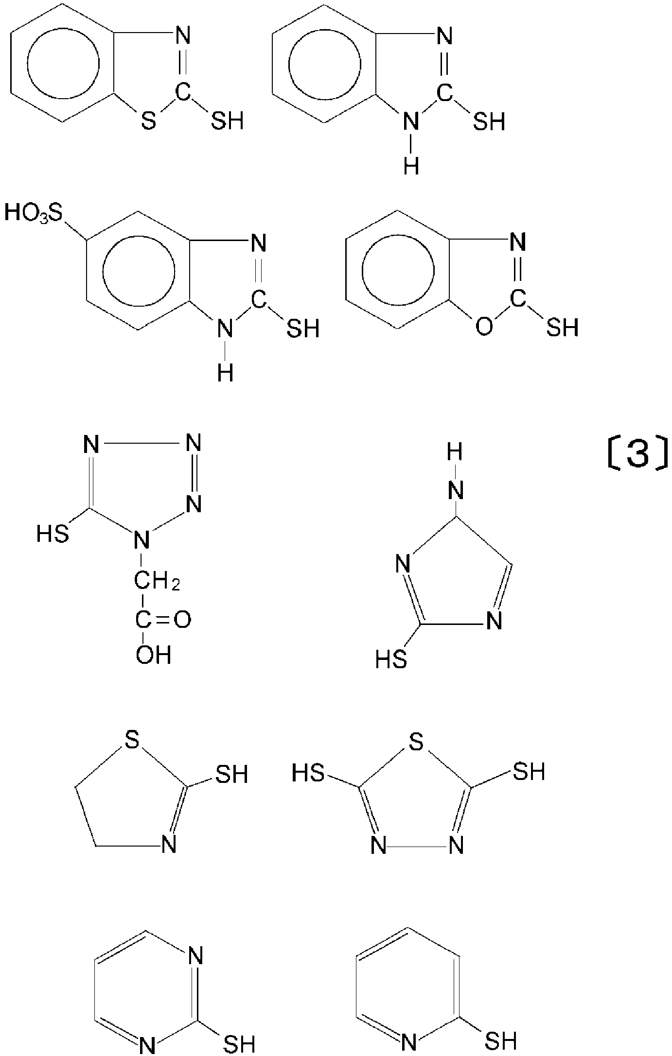


- The method for producing a metallic material for electronic components according to claim 26, wherein the surface treatment with the phosphoric acid ester-based solution is performed by applying the phosphoric acid ester-based solution to the outermost layer.
- The method for producing a metallic material for electronic components according to claim 26, wherein the surface treatment with the phosphoric acid ester-based solution is performed by conducting an electrolysis by immersing the metallic material after the formation of the outermost layer in the phosphoric acid ester-based solution and using as the anode the metallic material after the formation of the outermost layer.
- A connector terminal using, in the contact portion thereof, the metallic material for electronic components according to any one of claims 1 to 25.
- An FFC terminal using, in the contact portion thereof, the metallic material for electronic components according to any one of claims 1 to 25.
- An FPC terminal using, in the contact portion thereof, the metallic material for electronic components according to any one of claims 1 to 25.
- An electronic component using, in the electrode thereof for external connection, the metallic material for electronic components according to any one of claims 1 to 25.
- An electronic component using the metallic material for electronic components according to any one of claims 1 to 25, in a push-in type terminal thereof for fixing a board connection portion to a board by pushing the board connection portion into the through hole formed in the board, wherein a female terminal connection portion and the board connection portion are provided respectively on one side and the other side of a mounting portion to be attached to a housing.
Applications Claiming Priority (3)
| Application Number | Priority Date | Filing Date | Title |
|---|---|---|---|
| JP2012144652 | 2012-06-27 | ||
| JP2012259142A JP6050664B2 (en) | 2012-06-27 | 2012-11-27 | METAL MATERIAL FOR ELECTRONIC COMPONENT AND ITS MANUFACTURING METHOD, CONNECTOR TERMINAL USING THE SAME, CONNECTOR AND ELECTRONIC COMPONENT |
| PCT/JP2013/067728 WO2014003145A1 (en) | 2012-06-27 | 2013-06-27 | Electronic component metal material and manufacturing method thereof, and connector terminal, connector and electronic component using said electronic component metal material |
Publications (3)
| Publication Number | Publication Date |
|---|---|
| EP2868776A1 EP2868776A1 (en) | 2015-05-06 |
| EP2868776A4 EP2868776A4 (en) | 2016-03-02 |
| EP2868776B1 true EP2868776B1 (en) | 2017-05-17 |
Family
ID=49783280
Family Applications (1)
| Application Number | Title | Priority Date | Filing Date |
|---|---|---|---|
| EP13809664.9A Active EP2868776B1 (en) | 2012-06-27 | 2013-06-27 | Electronic component metal material and manufacturing method thereof, and connector terminal, connector and electronic component using said electronic component metal material |
Country Status (7)
| Country | Link |
|---|---|
| US (1) | US10530084B2 (en) |
| EP (1) | EP2868776B1 (en) |
| JP (1) | JP6050664B2 (en) |
| KR (1) | KR101649847B1 (en) |
| CN (1) | CN104379818B9 (en) |
| TW (1) | TWI466773B (en) |
| WO (1) | WO2014003145A1 (en) |
Families Citing this family (20)
| Publication number | Priority date | Publication date | Assignee | Title |
|---|---|---|---|---|
| JP5086485B1 (en) | 2011-09-20 | 2012-11-28 | Jx日鉱日石金属株式会社 | Metal material for electronic parts and method for producing the same |
| JP5284526B1 (en) | 2011-10-04 | 2013-09-11 | Jx日鉱日石金属株式会社 | Metal material for electronic parts and method for producing the same |
| TWI493798B (en) | 2012-02-03 | 2015-07-21 | Jx Nippon Mining & Metals Corp | Push-in terminals and electronic parts for their use |
| JP5138827B1 (en) | 2012-03-23 | 2013-02-06 | Jx日鉱日石金属株式会社 | Metal materials for electronic parts, connector terminals, connectors and electronic parts using the same |
| JP6050664B2 (en) | 2012-06-27 | 2016-12-21 | Jx金属株式会社 | METAL MATERIAL FOR ELECTRONIC COMPONENT AND ITS MANUFACTURING METHOD, CONNECTOR TERMINAL USING THE SAME, CONNECTOR AND ELECTRONIC COMPONENT |
| JP6029435B2 (en) | 2012-06-27 | 2016-11-24 | Jx金属株式会社 | METAL MATERIAL FOR ELECTRONIC COMPONENT AND ITS MANUFACTURING METHOD, CONNECTOR TERMINAL USING THE SAME, CONNECTOR AND ELECTRONIC COMPONENT |
| TWI485930B (en) * | 2012-10-04 | 2015-05-21 | Jx Nippon Mining & Metals Corp | Metal material for electronic parts and manufacturing method thereof |
| TWI488733B (en) * | 2012-10-04 | 2015-06-21 | Jx Nippon Mining & Metals Corp | Metal material for electronic parts and manufacturing method thereof |
| JP6332043B2 (en) * | 2015-01-09 | 2018-05-30 | 株式会社オートネットワーク技術研究所 | Connector terminal pair |
| JP6655325B2 (en) * | 2015-08-25 | 2020-02-26 | 株式会社エンプラス | Electrical contacts and sockets for electrical components |
| JP6750545B2 (en) * | 2016-05-19 | 2020-09-02 | 株式会社オートネットワーク技術研究所 | Press-fit terminal connection structure |
| CN106048680B (en) * | 2016-07-22 | 2018-05-22 | 东莞普瑞得五金塑胶制品有限公司 | A kind of corrosion resistant special coating of mobile phone fast charge interface energization |
| KR102148295B1 (en) * | 2018-07-26 | 2020-08-26 | 히로세코리아 주식회사 | Electrical contact terminal |
| JP7195201B2 (en) * | 2019-03-29 | 2022-12-23 | Dowaメタルテック株式会社 | Plating material and its manufacturing method |
| US11296436B2 (en) * | 2019-06-10 | 2022-04-05 | Rohm And Haas Electronic Materials Llc | Press-fit terminal with improved whisker inhibition |
| CN113381215A (en) * | 2019-10-30 | 2021-09-10 | 富士康(昆山)电脑接插件有限公司 | Conductive terminal |
| CN111525314B (en) * | 2020-05-05 | 2023-06-20 | 富士康(昆山)电脑接插件有限公司 | Conductive terminal |
| CN114094373A (en) * | 2020-06-22 | 2022-02-25 | 华为技术有限公司 | Conductive terminal, electric connector and electronic equipment |
| CN113066693A (en) * | 2021-02-18 | 2021-07-02 | 艾默生电气(珠海)有限公司 | Thermal fuse and metal shell for thermal fuse |
| EP4386113A1 (en) * | 2022-12-13 | 2024-06-19 | Aptiv Technologies Limited | Electrical terminal with metal conductive layer comprising silver |
Family Cites Families (66)
| Publication number | Priority date | Publication date | Assignee | Title |
|---|---|---|---|---|
| JPS461670Y1 (en) * | 1967-01-18 | 1971-01-20 | ||
| JPS5030587B1 (en) | 1969-07-02 | 1975-10-02 | ||
| GB2069005A (en) * | 1980-02-05 | 1981-08-19 | Plessey Co Ltd | Intermetallic connector contact finishes |
| US4529667A (en) | 1983-04-06 | 1985-07-16 | The Furukawa Electric Company, Ltd. | Silver-coated electric composite materials |
| JPS61124597A (en) | 1984-11-20 | 1986-06-12 | Furukawa Electric Co Ltd:The | Silver-coated electric material |
| JP2726434B2 (en) | 1988-06-06 | 1998-03-11 | 古河電気工業株式会社 | Sn or Sn alloy coating material |
| JP2670348B2 (en) | 1989-05-15 | 1997-10-29 | 古河電気工業株式会社 | Sn or Sn alloy coating material |
| DE4005836C2 (en) | 1990-02-23 | 1999-10-28 | Stolberger Metallwerke Gmbh | Electrical connector pair |
| JPH04160200A (en) | 1990-10-24 | 1992-06-03 | Furukawa Electric Co Ltd:The | Production of electric contact material |
| JP2959872B2 (en) | 1991-06-18 | 1999-10-06 | 古河電気工業株式会社 | Electrical contact material and its manufacturing method |
| JPH05311495A (en) * | 1991-12-25 | 1993-11-22 | Nikko Kinzoku Kk | Hole sealing treatment of noble metal plated material |
| JPH0681189A (en) * | 1992-09-02 | 1994-03-22 | Mitsubishi Shindoh Co Ltd | Production of plated copper sheet or plated copper alloy sheet for producing electric connector |
| JP2925986B2 (en) | 1995-09-08 | 1999-07-28 | 古河電気工業株式会社 | Fixed contact material or electrical contact parts consisting of a contact part and a terminal part |
| JP3701448B2 (en) | 1997-10-17 | 2005-09-28 | 株式会社オートネットワーク技術研究所 | Mating type connection terminal |
| JP4086949B2 (en) | 1998-02-10 | 2008-05-14 | 古河電気工業株式会社 | Metal coated member |
| JPH11279792A (en) * | 1998-03-27 | 1999-10-12 | Nippon Mining & Metals Co Ltd | Formation of tin-silver solder alloy plating layer |
| JPH11350189A (en) * | 1998-06-03 | 1999-12-21 | Furukawa Electric Co Ltd:The | Material for electrical and electronic parts, its production and electrical and electronic parts using the material |
| JPH11350188A (en) | 1998-06-03 | 1999-12-21 | Furukawa Electric Co Ltd:The | Material for electric and electronic parts, its production, and electric and electronic parts lising the same |
| JP4489232B2 (en) * | 1999-06-14 | 2010-06-23 | 日鉱金属株式会社 | Plating material for connectors |
| JP4465068B2 (en) | 1999-11-10 | 2010-05-19 | 日本リーロナール有限会社 | Method for forming silver-tin alloy plating layer |
| US6361823B1 (en) * | 1999-12-03 | 2002-03-26 | Atotech Deutschland Gmbh | Process for whisker-free aqueous electroless tin plating |
| JP3910363B2 (en) | 2000-12-28 | 2007-04-25 | 富士通株式会社 | External connection terminal |
| US6924044B2 (en) | 2001-08-14 | 2005-08-02 | Snag, Llc | Tin-silver coatings |
| JP3513709B2 (en) | 2001-10-16 | 2004-03-31 | 石原薬品株式会社 | Preventing tin whiskers by pretreatment |
| KR100513947B1 (en) * | 2002-03-29 | 2005-09-09 | 닛코 킨조쿠 가부시키가이샤 | A copper alloy having good pressing workability and manufacturing method therefor |
| JP3442764B1 (en) | 2002-08-22 | 2003-09-02 | エフシーエム株式会社 | Connector terminals and connectors |
| JP3519727B1 (en) | 2002-12-09 | 2004-04-19 | Fcm株式会社 | Connector terminal and connector having the same |
| TWI225322B (en) * | 2002-08-22 | 2004-12-11 | Fcm Co Ltd | Terminal having ruthenium layer and a connector with the terminal |
| JP3519726B1 (en) | 2002-11-26 | 2004-04-19 | Fcm株式会社 | Terminal and parts having it |
| KR100495184B1 (en) | 2002-12-02 | 2005-06-14 | 엘지마이크론 주식회사 | A tape substrate and tin plating method of the tape substrate |
| US7391116B2 (en) | 2003-10-14 | 2008-06-24 | Gbc Metals, Llc | Fretting and whisker resistant coating system and method |
| JP2005126763A (en) * | 2003-10-23 | 2005-05-19 | Furukawa Electric Co Ltd:The | Coating material, electric/electronic component using the same, rubber contact component using the same, and coating material manufacturing method |
| DE502004010902D1 (en) * | 2003-11-28 | 2010-04-29 | Wieland Werke Ag | Layer sequence for producing a composite material for electromechanical components |
| JP4302545B2 (en) | 2004-02-10 | 2009-07-29 | 株式会社オートネットワーク技術研究所 | Press-fit terminal |
| JP2005353542A (en) * | 2004-06-14 | 2005-12-22 | Furukawa Electric Co Ltd:The | Conductive covering material, manufacturing method thereof, and connector terminal or contact using the covering material |
| JP2006127939A (en) * | 2004-10-29 | 2006-05-18 | Sumitomo Electric Ind Ltd | Electric conductor and its manufacturing method |
| JP4111522B2 (en) | 2004-11-30 | 2008-07-02 | 日鉱金属株式会社 | Sn coated copper material and terminal |
| DE112006000095T5 (en) * | 2005-01-18 | 2008-04-17 | AUTONETWORKS Technologies, LTD., Yokkaichi | Press fit connection, method for the manufacture thereof, and connection arrangement between a press-fit connection and a circuit board |
| US20060292847A1 (en) | 2005-06-24 | 2006-12-28 | Schetty Robert A Iii | Silver barrier layers to minimize whisker growth in tin electrodeposits |
| JP4489738B2 (en) * | 2005-08-31 | 2010-06-23 | 日鉱金属株式会社 | Cu-Ni-Si-Zn alloy tin plating strip |
| KR100964063B1 (en) * | 2005-09-07 | 2010-06-16 | 닛코킨조쿠 가부시키가이샤 | Aqueous antioxidant for tin or tin alloy |
| JP2008021501A (en) | 2006-07-12 | 2008-01-31 | Hitachi Cable Ltd | Electrical part for wiring, manufacturing method thereof, and terminal connecting part |
| JP5255225B2 (en) * | 2007-03-29 | 2013-08-07 | 古河電気工業株式会社 | Plating material having lubricating particles, method for producing the same, and electric / electronic component using the same |
| JP5192878B2 (en) * | 2007-04-09 | 2013-05-08 | 古河電気工業株式会社 | Connectors and metal materials for connectors |
| JP5286893B2 (en) | 2007-04-27 | 2013-09-11 | 日立化成株式会社 | Connection terminal, semiconductor package using connection terminal, and method of manufacturing semiconductor package |
| EP2175052A1 (en) * | 2007-07-06 | 2010-04-14 | DDK Ltd. | Process for producing electronic component, and electronic component produced by the process |
| JP2009057630A (en) * | 2007-08-07 | 2009-03-19 | Mitsubishi Shindoh Co Ltd | Sn-PLATED CONDUCTIVE MATERIAL, METHOD FOR PRODUCING THE SAME, AND ELECTRICITY CARRYING COMPONENT |
| KR100878916B1 (en) * | 2007-09-17 | 2009-01-15 | 삼성전기주식회사 | Solder bump |
| EP2273621A4 (en) * | 2008-03-19 | 2011-07-13 | Furukawa Electric Co Ltd | Terminal for connector and process for producing the terminal for connector |
| JP5151950B2 (en) * | 2008-12-11 | 2013-02-27 | 三菱マテリアル株式会社 | Sn plating material and manufacturing method thereof |
| KR101301815B1 (en) | 2008-12-19 | 2013-08-29 | 제이엑스 닛코 닛세키 킨조쿠 가부시키가이샤 | Fuel cell separator material, fuel cell separator using same, fuel cell stack, and method for producing fuel cell separator material |
| JP4372835B1 (en) * | 2009-04-14 | 2009-11-25 | 三菱伸銅株式会社 | Conductive member and manufacturing method thereof |
| CN102395713B (en) | 2009-04-14 | 2014-07-16 | 三菱伸铜株式会社 | Conductive member and manufacturing method thereof |
| JP5396139B2 (en) * | 2009-05-08 | 2014-01-22 | 株式会社神戸製鋼所 | Press-fit terminal |
| JP2010267418A (en) * | 2009-05-12 | 2010-11-25 | Furukawa Electric Co Ltd:The | Connector |
| US20120107639A1 (en) * | 2009-06-29 | 2012-05-03 | Om Sangyo Co., Ltd. | Electrical component and method for manufacturing electrical components |
| JP5479789B2 (en) | 2009-07-03 | 2014-04-23 | 古河電気工業株式会社 | Metal materials for connectors |
| JP5612355B2 (en) | 2009-07-15 | 2014-10-22 | 株式会社Kanzacc | Plating structure and method of manufacturing electrical material |
| JP5280957B2 (en) * | 2009-07-28 | 2013-09-04 | 三菱伸銅株式会社 | Conductive member and manufacturing method thereof |
| US8956735B2 (en) | 2010-03-26 | 2015-02-17 | Kabushiki Kaisha Kobe Seiko Sho | Copper alloy and electrically conductive material for connecting parts, and mating-type connecting part and method for producing the same |
| JP2012036436A (en) * | 2010-08-05 | 2012-02-23 | Mitsubishi Materials Corp | Sn ALLOY PLATED CONDUCTIVE MATERIAL AND METHOD FOR PRODUCING THE SAME |
| JP5086485B1 (en) | 2011-09-20 | 2012-11-28 | Jx日鉱日石金属株式会社 | Metal material for electronic parts and method for producing the same |
| JP5284526B1 (en) | 2011-10-04 | 2013-09-11 | Jx日鉱日石金属株式会社 | Metal material for electronic parts and method for producing the same |
| JP6029435B2 (en) | 2012-06-27 | 2016-11-24 | Jx金属株式会社 | METAL MATERIAL FOR ELECTRONIC COMPONENT AND ITS MANUFACTURING METHOD, CONNECTOR TERMINAL USING THE SAME, CONNECTOR AND ELECTRONIC COMPONENT |
| JP6050664B2 (en) | 2012-06-27 | 2016-12-21 | Jx金属株式会社 | METAL MATERIAL FOR ELECTRONIC COMPONENT AND ITS MANUFACTURING METHOD, CONNECTOR TERMINAL USING THE SAME, CONNECTOR AND ELECTRONIC COMPONENT |
| JP5427945B2 (en) | 2012-06-27 | 2014-02-26 | Jx日鉱日石金属株式会社 | METAL MATERIAL FOR ELECTRONIC COMPONENT AND ITS MANUFACTURING METHOD, CONNECTOR TERMINAL USING THE SAME, CONNECTOR AND ELECTRONIC COMPONENT |
-
2012
- 2012-11-27 JP JP2012259142A patent/JP6050664B2/en active Active
-
2013
- 2013-06-27 TW TW102122919A patent/TWI466773B/en active
- 2013-06-27 CN CN201380034077.4A patent/CN104379818B9/en active Active
- 2013-06-27 US US14/411,789 patent/US10530084B2/en active Active
- 2013-06-27 EP EP13809664.9A patent/EP2868776B1/en active Active
- 2013-06-27 KR KR1020157002016A patent/KR101649847B1/en active IP Right Grant
- 2013-06-27 WO PCT/JP2013/067728 patent/WO2014003145A1/en active Application Filing
Also Published As
| Publication number | Publication date |
|---|---|
| KR20150053263A (en) | 2015-05-15 |
| US10530084B2 (en) | 2020-01-07 |
| TWI466773B (en) | 2015-01-01 |
| US20150171537A1 (en) | 2015-06-18 |
| WO2014003145A1 (en) | 2014-01-03 |
| JP6050664B2 (en) | 2016-12-21 |
| TW201412513A (en) | 2014-04-01 |
| EP2868776A4 (en) | 2016-03-02 |
| CN104379818B (en) | 2017-03-01 |
| CN104379818A (en) | 2015-02-25 |
| JP2014029007A (en) | 2014-02-13 |
| KR101649847B1 (en) | 2016-08-22 |
| CN104379818B9 (en) | 2017-04-12 |
| EP2868776A1 (en) | 2015-05-06 |
Similar Documents
| Publication | Publication Date | Title |
|---|---|---|
| EP2868776B1 (en) | Electronic component metal material and manufacturing method thereof, and connector terminal, connector and electronic component using said electronic component metal material | |
| EP2868773B1 (en) | Electronic component metal material and manufacturing method thereof, and connector terminal, connector and electronic component using said electronic component metal material | |
| EP2878704B1 (en) | Metal material for electronic components, method for producing same, connector terminal using same, connector and electronic component | |
| EP2868772B1 (en) | Electronic component metal material and manufacturing method thereof, and connector terminal, connector and electronic component using said electronic component metal material | |
| JP5667152B2 (en) | Surface treatment plating material, method for producing the same, and electronic component | |
| EP2829637A1 (en) | Metallic material for electronic component, connector terminal obtained using same, connector, and electronic component | |
| EP3575446B1 (en) | Surface-treated plated material, connector terminal, connector, ffc terminal, ffc, fpc and electronic component | |
| EP3584353A9 (en) | Metallic material for electronic component, method for manufacturing said metallic material, and connector terminal, connector, and electronic component in which said metallic material is used | |
| JP5275504B1 (en) | METAL MATERIAL FOR ELECTRONIC COMPONENT AND ITS MANUFACTURING METHOD, CONNECTOR TERMINAL USING THE SAME, CONNECTOR AND ELECTRONIC COMPONENT | |
| JP2014139345A (en) | Surface treatment plated material and production method of the same, and electronic component | |
| JP2015045051A (en) | Metallic material for electronic component, method for producing the same, and connector terminal, connector and electronic component using the same |
Legal Events
| Date | Code | Title | Description |
|---|---|---|---|
| PUAI | Public reference made under article 153(3) epc to a published international application that has entered the european phase |
Free format text: ORIGINAL CODE: 0009012 |
|
| 17P | Request for examination filed |
Effective date: 20150116 |
|
| AK | Designated contracting states |
Kind code of ref document: A1 Designated state(s): AL AT BE BG CH CY CZ DE DK EE ES FI FR GB GR HR HU IE IS IT LI LT LU LV MC MK MT NL NO PL PT RO RS SE SI SK SM TR |
|
| AX | Request for extension of the european patent |
Extension state: BA ME |
|
| DAX | Request for extension of the european patent (deleted) | ||
| RA4 | Supplementary search report drawn up and despatched (corrected) |
Effective date: 20160202 |
|
| RIC1 | Information provided on ipc code assigned before grant |
Ipc: C22C 5/02 20060101ALI20160127BHEP Ipc: H01R 13/03 20060101ALI20160127BHEP Ipc: C23C 18/16 20060101ALN20160127BHEP Ipc: C23C 28/02 20060101ALN20160127BHEP Ipc: C25D 9/06 20060101ALI20160127BHEP Ipc: H01B 1/02 20060101ALI20160127BHEP Ipc: C25D 5/50 20060101ALI20160127BHEP Ipc: C22C 13/00 20060101ALI20160127BHEP Ipc: C22C 28/00 20060101ALI20160127BHEP Ipc: C22C 5/04 20060101ALI20160127BHEP Ipc: C25D 7/00 20060101AFI20160127BHEP Ipc: C22C 5/06 20060101ALI20160127BHEP Ipc: C25D 5/10 20060101ALI20160127BHEP Ipc: H01B 5/02 20060101ALI20160127BHEP Ipc: C25D 11/36 20060101ALN20160127BHEP Ipc: C25D 5/48 20060101ALI20160127BHEP |
|
| RIC1 | Information provided on ipc code assigned before grant |
Ipc: B32B 15/01 20060101ALI20161017BHEP Ipc: C25D 3/46 20060101ALN20161017BHEP Ipc: C22C 13/00 20060101ALI20161017BHEP Ipc: C25D 7/00 20060101AFI20161017BHEP Ipc: C25D 5/10 20060101ALI20161017BHEP Ipc: C22C 28/00 20060101ALI20161017BHEP Ipc: C25D 3/30 20060101ALN20161017BHEP Ipc: C25D 5/48 20060101ALI20161017BHEP Ipc: H01B 5/02 20060101ALI20161017BHEP Ipc: C23C 28/02 20060101ALN20161017BHEP Ipc: C25D 3/38 20060101ALN20161017BHEP Ipc: H01B 1/02 20060101ALI20161017BHEP Ipc: C23C 18/16 20060101ALN20161017BHEP Ipc: C25D 11/36 20060101ALN20161017BHEP Ipc: C25D 3/12 20060101ALN20161017BHEP Ipc: C22C 5/06 20060101ALI20161017BHEP Ipc: H01R 13/03 20060101ALI20161017BHEP Ipc: C22C 5/04 20060101ALI20161017BHEP Ipc: C25D 5/50 20060101ALI20161017BHEP Ipc: C25D 3/18 20060101ALN20161017BHEP Ipc: C25D 9/06 20060101ALI20161017BHEP Ipc: C22C 5/02 20060101ALI20161017BHEP |
|
| RIC1 | Information provided on ipc code assigned before grant |
Ipc: C25D 9/06 20060101ALI20161025BHEP Ipc: C25D 3/38 20060101ALN20161025BHEP Ipc: H01B 5/02 20060101ALI20161025BHEP Ipc: C25D 11/36 20060101ALN20161025BHEP Ipc: C25D 5/10 20060101ALI20161025BHEP Ipc: B32B 15/01 20060101ALI20161025BHEP Ipc: H01B 1/02 20060101ALI20161025BHEP Ipc: C25D 3/18 20060101ALN20161025BHEP Ipc: C23C 18/16 20060101ALN20161025BHEP Ipc: C25D 3/30 20060101ALN20161025BHEP Ipc: C22C 28/00 20060101ALI20161025BHEP Ipc: C23C 28/02 20060101ALN20161025BHEP Ipc: C25D 5/50 20060101ALI20161025BHEP Ipc: H01R 13/03 20060101ALI20161025BHEP Ipc: C25D 5/48 20060101ALI20161025BHEP Ipc: C25D 3/46 20060101ALN20161025BHEP Ipc: C22C 5/06 20060101ALI20161025BHEP Ipc: C25D 7/00 20060101AFI20161025BHEP Ipc: C25D 3/12 20060101ALN20161025BHEP Ipc: C22C 5/04 20060101ALI20161025BHEP Ipc: C22C 5/02 20060101ALI20161025BHEP Ipc: C22C 13/00 20060101ALI20161025BHEP |
|
| GRAP | Despatch of communication of intention to grant a patent |
Free format text: ORIGINAL CODE: EPIDOSNIGR1 |
|
| INTG | Intention to grant announced |
Effective date: 20161212 |
|
| RIN1 | Information on inventor provided before grant (corrected) |
Inventor name: FUKAMACHI, KAZUHIKO Inventor name: SHIBUYA, YOSHITAKA Inventor name: KODAMA, ATSUSHI |
|
| GRAS | Grant fee paid |
Free format text: ORIGINAL CODE: EPIDOSNIGR3 |
|
| GRAA | (expected) grant |
Free format text: ORIGINAL CODE: 0009210 |
|
| AK | Designated contracting states |
Kind code of ref document: B1 Designated state(s): AL AT BE BG CH CY CZ DE DK EE ES FI FR GB GR HR HU IE IS IT LI LT LU LV MC MK MT NL NO PL PT RO RS SE SI SK SM TR |
|
| REG | Reference to a national code |
Ref country code: GB Ref legal event code: FG4D |
|
| REG | Reference to a national code |
Ref country code: CH Ref legal event code: EP |
|
| REG | Reference to a national code |
Ref country code: IE Ref legal event code: FG4D |
|
| REG | Reference to a national code |
Ref country code: AT Ref legal event code: REF Ref document number: 894554 Country of ref document: AT Kind code of ref document: T Effective date: 20170615 |
|
| REG | Reference to a national code |
Ref country code: FR Ref legal event code: PLFP Year of fee payment: 5 |
|
| REG | Reference to a national code |
Ref country code: DE Ref legal event code: R096 Ref document number: 602013021375 Country of ref document: DE |
|
| REG | Reference to a national code |
Ref country code: NL Ref legal event code: MP Effective date: 20170517 |
|
| REG | Reference to a national code |
Ref country code: LT Ref legal event code: MG4D |
|
| REG | Reference to a national code |
Ref country code: AT Ref legal event code: MK05 Ref document number: 894554 Country of ref document: AT Kind code of ref document: T Effective date: 20170517 |
|
| PG25 | Lapsed in a contracting state [announced via postgrant information from national office to epo] |
Ref country code: LT Free format text: LAPSE BECAUSE OF FAILURE TO SUBMIT A TRANSLATION OF THE DESCRIPTION OR TO PAY THE FEE WITHIN THE PRESCRIBED TIME-LIMIT Effective date: 20170517 Ref country code: GR Free format text: LAPSE BECAUSE OF FAILURE TO SUBMIT A TRANSLATION OF THE DESCRIPTION OR TO PAY THE FEE WITHIN THE PRESCRIBED TIME-LIMIT Effective date: 20170818 Ref country code: NO Free format text: LAPSE BECAUSE OF FAILURE TO SUBMIT A TRANSLATION OF THE DESCRIPTION OR TO PAY THE FEE WITHIN THE PRESCRIBED TIME-LIMIT Effective date: 20170817 Ref country code: AT Free format text: LAPSE BECAUSE OF FAILURE TO SUBMIT A TRANSLATION OF THE DESCRIPTION OR TO PAY THE FEE WITHIN THE PRESCRIBED TIME-LIMIT Effective date: 20170517 Ref country code: HR Free format text: LAPSE BECAUSE OF FAILURE TO SUBMIT A TRANSLATION OF THE DESCRIPTION OR TO PAY THE FEE WITHIN THE PRESCRIBED TIME-LIMIT Effective date: 20170517 Ref country code: FI Free format text: LAPSE BECAUSE OF FAILURE TO SUBMIT A TRANSLATION OF THE DESCRIPTION OR TO PAY THE FEE WITHIN THE PRESCRIBED TIME-LIMIT Effective date: 20170517 Ref country code: ES Free format text: LAPSE BECAUSE OF FAILURE TO SUBMIT A TRANSLATION OF THE DESCRIPTION OR TO PAY THE FEE WITHIN THE PRESCRIBED TIME-LIMIT Effective date: 20170517 |
|
| PG25 | Lapsed in a contracting state [announced via postgrant information from national office to epo] |
Ref country code: IS Free format text: LAPSE BECAUSE OF FAILURE TO SUBMIT A TRANSLATION OF THE DESCRIPTION OR TO PAY THE FEE WITHIN THE PRESCRIBED TIME-LIMIT Effective date: 20170917 Ref country code: NL Free format text: LAPSE BECAUSE OF FAILURE TO SUBMIT A TRANSLATION OF THE DESCRIPTION OR TO PAY THE FEE WITHIN THE PRESCRIBED TIME-LIMIT Effective date: 20170517 Ref country code: RS Free format text: LAPSE BECAUSE OF FAILURE TO SUBMIT A TRANSLATION OF THE DESCRIPTION OR TO PAY THE FEE WITHIN THE PRESCRIBED TIME-LIMIT Effective date: 20170517 Ref country code: PL Free format text: LAPSE BECAUSE OF FAILURE TO SUBMIT A TRANSLATION OF THE DESCRIPTION OR TO PAY THE FEE WITHIN THE PRESCRIBED TIME-LIMIT Effective date: 20170517 Ref country code: SE Free format text: LAPSE BECAUSE OF FAILURE TO SUBMIT A TRANSLATION OF THE DESCRIPTION OR TO PAY THE FEE WITHIN THE PRESCRIBED TIME-LIMIT Effective date: 20170517 Ref country code: BG Free format text: LAPSE BECAUSE OF FAILURE TO SUBMIT A TRANSLATION OF THE DESCRIPTION OR TO PAY THE FEE WITHIN THE PRESCRIBED TIME-LIMIT Effective date: 20170817 Ref country code: LV Free format text: LAPSE BECAUSE OF FAILURE TO SUBMIT A TRANSLATION OF THE DESCRIPTION OR TO PAY THE FEE WITHIN THE PRESCRIBED TIME-LIMIT Effective date: 20170517 |
|
| PG25 | Lapsed in a contracting state [announced via postgrant information from national office to epo] |
Ref country code: RO Free format text: LAPSE BECAUSE OF FAILURE TO SUBMIT A TRANSLATION OF THE DESCRIPTION OR TO PAY THE FEE WITHIN THE PRESCRIBED TIME-LIMIT Effective date: 20170517 Ref country code: DK Free format text: LAPSE BECAUSE OF FAILURE TO SUBMIT A TRANSLATION OF THE DESCRIPTION OR TO PAY THE FEE WITHIN THE PRESCRIBED TIME-LIMIT Effective date: 20170517 Ref country code: SK Free format text: LAPSE BECAUSE OF FAILURE TO SUBMIT A TRANSLATION OF THE DESCRIPTION OR TO PAY THE FEE WITHIN THE PRESCRIBED TIME-LIMIT Effective date: 20170517 Ref country code: EE Free format text: LAPSE BECAUSE OF FAILURE TO SUBMIT A TRANSLATION OF THE DESCRIPTION OR TO PAY THE FEE WITHIN THE PRESCRIBED TIME-LIMIT Effective date: 20170517 Ref country code: CZ Free format text: LAPSE BECAUSE OF FAILURE TO SUBMIT A TRANSLATION OF THE DESCRIPTION OR TO PAY THE FEE WITHIN THE PRESCRIBED TIME-LIMIT Effective date: 20170517 |
|
| REG | Reference to a national code |
Ref country code: CH Ref legal event code: PL |
|
| REG | Reference to a national code |
Ref country code: DE Ref legal event code: R097 Ref document number: 602013021375 Country of ref document: DE |
|
| PG25 | Lapsed in a contracting state [announced via postgrant information from national office to epo] |
Ref country code: SM Free format text: LAPSE BECAUSE OF FAILURE TO SUBMIT A TRANSLATION OF THE DESCRIPTION OR TO PAY THE FEE WITHIN THE PRESCRIBED TIME-LIMIT Effective date: 20170517 Ref country code: IT Free format text: LAPSE BECAUSE OF FAILURE TO SUBMIT A TRANSLATION OF THE DESCRIPTION OR TO PAY THE FEE WITHIN THE PRESCRIBED TIME-LIMIT Effective date: 20170517 |
|
| PLBE | No opposition filed within time limit |
Free format text: ORIGINAL CODE: 0009261 |
|
| STAA | Information on the status of an ep patent application or granted ep patent |
Free format text: STATUS: NO OPPOSITION FILED WITHIN TIME LIMIT |
|
| REG | Reference to a national code |
Ref country code: IE Ref legal event code: MM4A |
|
| 26N | No opposition filed |
Effective date: 20180220 |
|
| PG25 | Lapsed in a contracting state [announced via postgrant information from national office to epo] |
Ref country code: IE Free format text: LAPSE BECAUSE OF NON-PAYMENT OF DUE FEES Effective date: 20170627 Ref country code: LI Free format text: LAPSE BECAUSE OF NON-PAYMENT OF DUE FEES Effective date: 20170630 Ref country code: LU Free format text: LAPSE BECAUSE OF NON-PAYMENT OF DUE FEES Effective date: 20170627 Ref country code: CH Free format text: LAPSE BECAUSE OF NON-PAYMENT OF DUE FEES Effective date: 20170630 |
|
| REG | Reference to a national code |
Ref country code: FR Ref legal event code: PLFP Year of fee payment: 6 |
|
| PG25 | Lapsed in a contracting state [announced via postgrant information from national office to epo] |
Ref country code: SI Free format text: LAPSE BECAUSE OF FAILURE TO SUBMIT A TRANSLATION OF THE DESCRIPTION OR TO PAY THE FEE WITHIN THE PRESCRIBED TIME-LIMIT Effective date: 20170517 |
|
| REG | Reference to a national code |
Ref country code: BE Ref legal event code: MM Effective date: 20170630 |
|
| PG25 | Lapsed in a contracting state [announced via postgrant information from national office to epo] |
Ref country code: BE Free format text: LAPSE BECAUSE OF NON-PAYMENT OF DUE FEES Effective date: 20170630 |
|
| PG25 | Lapsed in a contracting state [announced via postgrant information from national office to epo] |
Ref country code: MT Free format text: LAPSE BECAUSE OF NON-PAYMENT OF DUE FEES Effective date: 20170627 |
|
| PG25 | Lapsed in a contracting state [announced via postgrant information from national office to epo] |
Ref country code: MC Free format text: LAPSE BECAUSE OF FAILURE TO SUBMIT A TRANSLATION OF THE DESCRIPTION OR TO PAY THE FEE WITHIN THE PRESCRIBED TIME-LIMIT Effective date: 20170517 Ref country code: HU Free format text: LAPSE BECAUSE OF FAILURE TO SUBMIT A TRANSLATION OF THE DESCRIPTION OR TO PAY THE FEE WITHIN THE PRESCRIBED TIME-LIMIT; INVALID AB INITIO Effective date: 20130627 |
|
| PG25 | Lapsed in a contracting state [announced via postgrant information from national office to epo] |
Ref country code: CY Free format text: LAPSE BECAUSE OF FAILURE TO SUBMIT A TRANSLATION OF THE DESCRIPTION OR TO PAY THE FEE WITHIN THE PRESCRIBED TIME-LIMIT Effective date: 20170517 |
|
| PG25 | Lapsed in a contracting state [announced via postgrant information from national office to epo] |
Ref country code: MK Free format text: LAPSE BECAUSE OF FAILURE TO SUBMIT A TRANSLATION OF THE DESCRIPTION OR TO PAY THE FEE WITHIN THE PRESCRIBED TIME-LIMIT Effective date: 20170517 |
|
| PG25 | Lapsed in a contracting state [announced via postgrant information from national office to epo] |
Ref country code: TR Free format text: LAPSE BECAUSE OF FAILURE TO SUBMIT A TRANSLATION OF THE DESCRIPTION OR TO PAY THE FEE WITHIN THE PRESCRIBED TIME-LIMIT Effective date: 20170517 |
|
| PG25 | Lapsed in a contracting state [announced via postgrant information from national office to epo] |
Ref country code: PT Free format text: LAPSE BECAUSE OF FAILURE TO SUBMIT A TRANSLATION OF THE DESCRIPTION OR TO PAY THE FEE WITHIN THE PRESCRIBED TIME-LIMIT Effective date: 20170517 |
|
| PG25 | Lapsed in a contracting state [announced via postgrant information from national office to epo] |
Ref country code: AL Free format text: LAPSE BECAUSE OF FAILURE TO SUBMIT A TRANSLATION OF THE DESCRIPTION OR TO PAY THE FEE WITHIN THE PRESCRIBED TIME-LIMIT Effective date: 20170517 |
|
| PGFP | Annual fee paid to national office [announced via postgrant information from national office to epo] |
Ref country code: FR Payment date: 20230510 Year of fee payment: 11 Ref country code: DE Payment date: 20230502 Year of fee payment: 11 |
|
| PGFP | Annual fee paid to national office [announced via postgrant information from national office to epo] |
Ref country code: GB Payment date: 20230504 Year of fee payment: 11 |