EP2863446A2 - Flexible organische lichtemittierende Diodenanzeige und Herstellungsverfahren dafür - Google Patents
Flexible organische lichtemittierende Diodenanzeige und Herstellungsverfahren dafür Download PDFInfo
- Publication number
- EP2863446A2 EP2863446A2 EP14188721.6A EP14188721A EP2863446A2 EP 2863446 A2 EP2863446 A2 EP 2863446A2 EP 14188721 A EP14188721 A EP 14188721A EP 2863446 A2 EP2863446 A2 EP 2863446A2
- Authority
- EP
- European Patent Office
- Prior art keywords
- layer
- inorganic layer
- inorganic
- patterns
- layer patterns
- Prior art date
- Legal status (The legal status is an assumption and is not a legal conclusion. Google has not performed a legal analysis and makes no representation as to the accuracy of the status listed.)
- Granted
Links
- 238000004519 manufacturing process Methods 0.000 title claims description 11
- 239000010410 layer Substances 0.000 claims abstract description 344
- 239000010409 thin film Substances 0.000 claims abstract description 75
- 238000005538 encapsulation Methods 0.000 claims abstract description 62
- 239000012044 organic layer Substances 0.000 claims abstract description 52
- 239000000758 substrate Substances 0.000 claims abstract description 27
- 238000000151 deposition Methods 0.000 claims description 31
- 239000011159 matrix material Substances 0.000 claims description 17
- 230000008021 deposition Effects 0.000 claims description 15
- 238000005530 etching Methods 0.000 claims description 12
- 238000005452 bending Methods 0.000 claims description 9
- 238000000059 patterning Methods 0.000 claims description 9
- 238000000034 method Methods 0.000 claims 2
- 239000003990 capacitor Substances 0.000 description 14
- 239000004642 Polyimide Substances 0.000 description 7
- 229920001721 polyimide Polymers 0.000 description 7
- 239000010408 film Substances 0.000 description 5
- 230000007935 neutral effect Effects 0.000 description 5
- -1 polyethylene terephthalate Polymers 0.000 description 5
- 238000002347 injection Methods 0.000 description 4
- 239000007924 injection Substances 0.000 description 4
- PQXKHYXIUOZZFA-UHFFFAOYSA-M lithium fluoride Chemical compound [Li+].[F-] PQXKHYXIUOZZFA-UHFFFAOYSA-M 0.000 description 4
- 239000000463 material Substances 0.000 description 4
- VYPSYNLAJGMNEJ-UHFFFAOYSA-N Silicium dioxide Chemical compound O=[Si]=O VYPSYNLAJGMNEJ-UHFFFAOYSA-N 0.000 description 3
- 230000004888 barrier function Effects 0.000 description 3
- 238000005516 engineering process Methods 0.000 description 3
- 229910052751 metal Inorganic materials 0.000 description 3
- 239000002184 metal Substances 0.000 description 3
- 229910052814 silicon oxide Inorganic materials 0.000 description 3
- RTZKZFJDLAIYFH-UHFFFAOYSA-N Diethyl ether Chemical compound CCOCC RTZKZFJDLAIYFH-UHFFFAOYSA-N 0.000 description 2
- 239000004593 Epoxy Substances 0.000 description 2
- 239000004698 Polyethylene Substances 0.000 description 2
- 229910004205 SiNX Inorganic materials 0.000 description 2
- GWEVSGVZZGPLCZ-UHFFFAOYSA-N Titan oxide Chemical compound O=[Ti]=O GWEVSGVZZGPLCZ-UHFFFAOYSA-N 0.000 description 2
- 229910021417 amorphous silicon Inorganic materials 0.000 description 2
- 230000007547 defect Effects 0.000 description 2
- 230000005283 ground state Effects 0.000 description 2
- 150000002500 ions Chemical class 0.000 description 2
- 239000002346 layers by function Substances 0.000 description 2
- 238000012986 modification Methods 0.000 description 2
- 230000004048 modification Effects 0.000 description 2
- 229920000515 polycarbonate Polymers 0.000 description 2
- 239000004417 polycarbonate Substances 0.000 description 2
- 229920000573 polyethylene Polymers 0.000 description 2
- 239000004065 semiconductor Substances 0.000 description 2
- 239000002356 single layer Substances 0.000 description 2
- 239000004695 Polyether sulfone Substances 0.000 description 1
- 239000004697 Polyetherimide Substances 0.000 description 1
- 229910020286 SiOxNy Inorganic materials 0.000 description 1
- 230000005856 abnormality Effects 0.000 description 1
- PNEYBMLMFCGWSK-UHFFFAOYSA-N aluminium oxide Inorganic materials [O-2].[O-2].[O-2].[Al+3].[Al+3] PNEYBMLMFCGWSK-UHFFFAOYSA-N 0.000 description 1
- 230000003466 anti-cipated effect Effects 0.000 description 1
- QVGXLLKOCUKJST-UHFFFAOYSA-N atomic oxygen Chemical compound [O] QVGXLLKOCUKJST-UHFFFAOYSA-N 0.000 description 1
- 229910010293 ceramic material Inorganic materials 0.000 description 1
- 229910000424 chromium(II) oxide Inorganic materials 0.000 description 1
- 239000002131 composite material Substances 0.000 description 1
- 239000003989 dielectric material Substances 0.000 description 1
- 230000005281 excited state Effects 0.000 description 1
- 229920002457 flexible plastic Polymers 0.000 description 1
- 230000014509 gene expression Effects 0.000 description 1
- 239000011229 interlayer Substances 0.000 description 1
- CPLXHLVBOLITMK-UHFFFAOYSA-N magnesium oxide Inorganic materials [Mg]=O CPLXHLVBOLITMK-UHFFFAOYSA-N 0.000 description 1
- 229910044991 metal oxide Inorganic materials 0.000 description 1
- 150000004706 metal oxides Chemical class 0.000 description 1
- 150000004767 nitrides Chemical class 0.000 description 1
- 239000011368 organic material Substances 0.000 description 1
- 229910052760 oxygen Inorganic materials 0.000 description 1
- 239000001301 oxygen Substances 0.000 description 1
- 238000002161 passivation Methods 0.000 description 1
- XNGIFLGASWRNHJ-UHFFFAOYSA-L phthalate(2-) Chemical compound [O-]C(=O)C1=CC=CC=C1C([O-])=O XNGIFLGASWRNHJ-UHFFFAOYSA-L 0.000 description 1
- 239000004033 plastic Substances 0.000 description 1
- 229920003023 plastic Polymers 0.000 description 1
- 229920003207 poly(ethylene-2,6-naphthalate) Polymers 0.000 description 1
- 229920000058 polyacrylate Polymers 0.000 description 1
- 229920001230 polyarylate Polymers 0.000 description 1
- 229910021420 polycrystalline silicon Inorganic materials 0.000 description 1
- 229920006393 polyether sulfone Polymers 0.000 description 1
- 229920001601 polyetherimide Polymers 0.000 description 1
- 239000011112 polyethylene naphthalate Substances 0.000 description 1
- 229920000139 polyethylene terephthalate Polymers 0.000 description 1
- 239000005020 polyethylene terephthalate Substances 0.000 description 1
- 229920000642 polymer Polymers 0.000 description 1
- 229920005591 polysilicon Polymers 0.000 description 1
- 230000035939 shock Effects 0.000 description 1
- 238000004544 sputter deposition Methods 0.000 description 1
- 229910001220 stainless steel Inorganic materials 0.000 description 1
- 239000010935 stainless steel Substances 0.000 description 1
- 239000012780 transparent material Substances 0.000 description 1
Images





Classifications
-
- H—ELECTRICITY
- H10—SEMICONDUCTOR DEVICES; ELECTRIC SOLID-STATE DEVICES NOT OTHERWISE PROVIDED FOR
- H10K—ORGANIC ELECTRIC SOLID-STATE DEVICES
- H10K59/00—Integrated devices, or assemblies of multiple devices, comprising at least one organic light-emitting element covered by group H10K50/00
- H10K59/80—Constructional details
- H10K59/87—Passivation; Containers; Encapsulations
- H10K59/873—Encapsulations
- H10K59/8731—Encapsulations multilayered coatings having a repetitive structure, e.g. having multiple organic-inorganic bilayers
-
- H—ELECTRICITY
- H10—SEMICONDUCTOR DEVICES; ELECTRIC SOLID-STATE DEVICES NOT OTHERWISE PROVIDED FOR
- H10K—ORGANIC ELECTRIC SOLID-STATE DEVICES
- H10K50/00—Organic light-emitting devices
- H10K50/80—Constructional details
- H10K50/84—Passivation; Containers; Encapsulations
- H10K50/844—Encapsulations
-
- H—ELECTRICITY
- H10—SEMICONDUCTOR DEVICES; ELECTRIC SOLID-STATE DEVICES NOT OTHERWISE PROVIDED FOR
- H10K—ORGANIC ELECTRIC SOLID-STATE DEVICES
- H10K50/00—Organic light-emitting devices
- H10K50/80—Constructional details
- H10K50/84—Passivation; Containers; Encapsulations
- H10K50/844—Encapsulations
- H10K50/8445—Encapsulations multilayered coatings having a repetitive structure, e.g. having multiple organic-inorganic bilayers
-
- H—ELECTRICITY
- H10—SEMICONDUCTOR DEVICES; ELECTRIC SOLID-STATE DEVICES NOT OTHERWISE PROVIDED FOR
- H10K—ORGANIC ELECTRIC SOLID-STATE DEVICES
- H10K59/00—Integrated devices, or assemblies of multiple devices, comprising at least one organic light-emitting element covered by group H10K50/00
- H10K59/10—OLED displays
-
- H—ELECTRICITY
- H10—SEMICONDUCTOR DEVICES; ELECTRIC SOLID-STATE DEVICES NOT OTHERWISE PROVIDED FOR
- H10K—ORGANIC ELECTRIC SOLID-STATE DEVICES
- H10K71/00—Manufacture or treatment specially adapted for the organic devices covered by this subclass
-
- H—ELECTRICITY
- H10—SEMICONDUCTOR DEVICES; ELECTRIC SOLID-STATE DEVICES NOT OTHERWISE PROVIDED FOR
- H10K—ORGANIC ELECTRIC SOLID-STATE DEVICES
- H10K77/00—Constructional details of devices covered by this subclass and not covered by groups H10K10/80, H10K30/80, H10K50/80 or H10K59/80
- H10K77/10—Substrates, e.g. flexible substrates
- H10K77/111—Flexible substrates
-
- H—ELECTRICITY
- H10—SEMICONDUCTOR DEVICES; ELECTRIC SOLID-STATE DEVICES NOT OTHERWISE PROVIDED FOR
- H10K—ORGANIC ELECTRIC SOLID-STATE DEVICES
- H10K2102/00—Constructional details relating to the organic devices covered by this subclass
- H10K2102/301—Details of OLEDs
- H10K2102/311—Flexible OLED
-
- H—ELECTRICITY
- H10—SEMICONDUCTOR DEVICES; ELECTRIC SOLID-STATE DEVICES NOT OTHERWISE PROVIDED FOR
- H10K—ORGANIC ELECTRIC SOLID-STATE DEVICES
- H10K59/00—Integrated devices, or assemblies of multiple devices, comprising at least one organic light-emitting element covered by group H10K50/00
- H10K59/10—OLED displays
- H10K59/12—Active-matrix OLED [AMOLED] displays
-
- Y—GENERAL TAGGING OF NEW TECHNOLOGICAL DEVELOPMENTS; GENERAL TAGGING OF CROSS-SECTIONAL TECHNOLOGIES SPANNING OVER SEVERAL SECTIONS OF THE IPC; TECHNICAL SUBJECTS COVERED BY FORMER USPC CROSS-REFERENCE ART COLLECTIONS [XRACs] AND DIGESTS
- Y02—TECHNOLOGIES OR APPLICATIONS FOR MITIGATION OR ADAPTATION AGAINST CLIMATE CHANGE
- Y02E—REDUCTION OF GREENHOUSE GAS [GHG] EMISSIONS, RELATED TO ENERGY GENERATION, TRANSMISSION OR DISTRIBUTION
- Y02E10/00—Energy generation through renewable energy sources
- Y02E10/50—Photovoltaic [PV] energy
- Y02E10/549—Organic PV cells
-
- Y—GENERAL TAGGING OF NEW TECHNOLOGICAL DEVELOPMENTS; GENERAL TAGGING OF CROSS-SECTIONAL TECHNOLOGIES SPANNING OVER SEVERAL SECTIONS OF THE IPC; TECHNICAL SUBJECTS COVERED BY FORMER USPC CROSS-REFERENCE ART COLLECTIONS [XRACs] AND DIGESTS
- Y02—TECHNOLOGIES OR APPLICATIONS FOR MITIGATION OR ADAPTATION AGAINST CLIMATE CHANGE
- Y02P—CLIMATE CHANGE MITIGATION TECHNOLOGIES IN THE PRODUCTION OR PROCESSING OF GOODS
- Y02P70/00—Climate change mitigation technologies in the production process for final industrial or consumer products
- Y02P70/50—Manufacturing or production processes characterised by the final manufactured product
Definitions
- the described technology relates generally to a flexible organic light emitting diode display and a manufacturing method thereof, and more particularly, to a flexible organic light emitting diode display having a thin film encapsulation layer structure including a plurality of inorganic and organic layers.
- An organic light emitting diode (OLED) display includes organic light emitting diodes (OLEDs), each of which includes a hole injection electrode, an organic emission layer, and an electron injection electrode.
- Each OLED emits light using (utilizing) energy generated when electrons and holes are combined to create exitons in the organic emission layer and the exitons fall from an exited state to a ground state.
- the OLED display can be easily bendable and is advantageous in forming a slim structure.
- a picture abnormality does not occur in the OLED display when (e.g., only when) the OLEDs are positioned at (e.g., in) the neutral plane.
- the thickness of the organic light emitting diode display is increased by internal and external films such as a polarizing film and a passivation film attached to the organic light emitting diode display, the tensile stress and the compressive stress are increased such that the neutral plane becomes narrow, thereby making it difficult to position the organic light emitting element at the neutral plane.
- the OLED display has a structure in which composite materials are layered and thus asymmetry of strains occurs due to a difference between tensile stress and compressive stress that are applied to outer and inner sides of a bent portion. Accordingly, it is difficult to position the OLED at the neutral plane, thereby causing display defects.
- a moisture permeation path may be created in a display area through cracks formed due to excessive stress.
- deformation of organic and inorganic layers forming a thin film encapsulation layer may cause deformation of the display area or other defects.
- An aspect of an embodiment of the described technology has been made in an effort to provide a flexible organic light emitting diode (OLED) display having advantages of preventing or reducing cracks from being generated at inorganic layers of a thin film encapsulation layer and/or preventing or reducing moisture permeation into the display area from the thin film encapsulation layer when the flexible OLED display is bent or folded.
- OLED organic light emitting diode
- a flexible organic light emitting diode (OLED) display includes: a substrate; an organic light emitting diode (OLED) layer provided on the substrate; and a thin film encapsulation layer provided on the OLED layer.
- the thin film encapsulation layer includes: a plurality of laminated inorganic layers, at least one inorganic layer of the plurality of inorganic layers including a plurality of inorganic layer patterns that are disposed to be spaced apart from each other on a plane; and an organic layer formed between the plurality of inorganic layer patterns.
- the at least one inorganic layer, the plurality of inorganic layer patterns, and the organic layer may be respectively a first inorganic layer, first inorganic layer patterns, and a first organic layer, and a second inorganic layer may be disposed on the first organic layer and may include a plurality of second inorganic layer patterns that are disposed between the first inorganic layer patterns to be spaced apart from each other.
- the flexible OLED display may further include: a second organic layer disposed between the plurality of second inorganic layer patterns; and a third inorganic layer disposed on the second organic layer and including a plurality of third inorganic layer patterns that are disposed between the second inorganic layer patterns to be spaced apart from each other.
- the first and second inorganic layer patterns may partially contact each other.
- the plurality of inorganic layers may be disposed above an organic emission layer of the organic light emitting diode layer.
- the plurality of inorganic layer patterns may be coupled to each other through the inorganic layer patterns of the inorganic layers of the respective different layers.
- the plurality of inorganic layer patterns may be formed in a matrix form in which a square shape is repeatedly disposed on a plane.
- the plurality of inorganic layer patterns may be formed in a matrix form in which a circular shape is repeatedly disposed on a plane.
- the plurality of inorganic layer patterns may be formed in a matrix form in which a rectangular shape is repeatedly disposed on a plane.
- the plurality of inorganic layer patterns may be arranged in a direction along which the substrate is bendable.
- the plurality of inorganic layer patterns may be formed in a matrix form in which a triangular pyramidal shape is repeatedly disposed.
- the plurality of inorganic layer patterns may respectively have different sizes in a bending region where the substrate is bent and in an unbending region where the substrate is not bent.
- a manufacturing method of a flexible OLED display includes: forming an OLED layer including an anode coupled to a transistor, an organic emission layer on the anode, and a cathode on the organic emission layer, on a substrate, and forming a thin film encapsulation layer on the OLED layer.
- the forming of the thin film encapsulation layer includes: a first deposition act of depositing a first inorganic layer on the OLED layer; a first etching act of patterning the first inorganic layer to include a plurality of first inorganic layer patterns that are disposed to be spaced apart from each other; a second deposition act of depositing a first organic layer between the patterned first inorganic layer patterns using (utilizing) a first mask; a third deposition act of depositing a second inorganic layer on the first organic layer; and a second etching act of patterning the second inorganic layer to include a plurality of second inorganic layer patterns that are disposed to be spaced apart from each other.
- the manufacturing method of the flexible OLED display according to the exemplary embodiment may further include, after the second etching act: a fourth deposition act of depositing a second organic layer between the patterned second inorganic layer patterns; a fifth deposition act of depositing a third inorganic layer on the second organic layer; and a third etching act of patterning the third inorganic layer to include a plurality of third inorganic layer patterns that are disposed to be spaced apart from each other.
- the stress of the inorganic layers are alleviated by the inorganic layer patterns of the inorganic layers of the thin film encapsulation layer, thereby preventing the cracks from being generated at the inorganic layer and/or the moisture permeation into the display area from the thin film encapsulation layer.
- spatially relative terms such as “beneath”, “below”, “lower”, “under”, “above”, “upper” and the like, may be used herein for ease of description to describe one element or feature's relationship to another element(s) or feature(s) as illustrated in the figures. It will be understood that the spatially relative terms are intended to encompass different orientations of the device in use or in operation, in addition to the orientation depicted in the figures. For example, if the device in the figures is turned over, elements described as “below” or “beneath” or “under” other elements or features would then be oriented “above” the other elements or features. Thus, the example terms “below” and “under” can encompass both an orientation of above and below.
- the device may be otherwise oriented (e.g., rotated 90 degrees or at other orientations) and the spatially relative descriptors used herein should be interpreted accordingly.
- a layer when referred to as being "between" two layers, it can be the only layer between the two layers, or one or more intervening layers may also be present.
- the exemplary embodiments are not limited to certain forms of the regions illustrated, but may include forms that are modified through manufacturing, for example.
- OLED organic light emitting diode
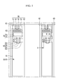
- FIG. 1 is a layout view of a pixel structure of a flexible organic light emitting diode (OLED) display according to an exemplary embodiment
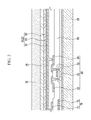
- FIG. 2 is a drawing showing a cross-section of the OLED display taken along the line II-II of FIG. 1 .
- the OLED display includes a pixel circuit and an organic light emitting diode (OLED) that are formed in each pixel.
- OLED organic light emitting diode
- each pixel circuit includes a switching thin film transistor 50, a driving thin film transistor 60, and a capacitor 70.
- the flexible OLED display includes: a gate line 81 that extends along a first direction; and a data line 82 and a driving voltage line 83 that are insulated from the gate line 81 and extend along a second direction crossing the first direction.
- one pixel may be defined by a boundary of the gate line 81, the data line 82, and the driving voltage line 83, but it is not necessarily limited thereto.
- Each pixel is a basic unit for displaying an image
- the flexible OLED display displays the image using (utilizing) a plurality of pixels.
- FIGS. 1 and 2 an active matrix flexible display device having a 2Tr-1 Cap structure where two thin film transistors 50 and 60 and one capacitor 70 are provided in one pixel is illustrated, but the structure of the flexible OLED display is not limited to the illustrated example.
- the flexible OLED display may include three or more thin film transistors and two or more capacitors, and additional wires may be further formed therein to have various suitable structures.
- the OLED includes an anode 91, an organic emission layer 92, and a cathode 93.
- One of the anode 91 and the cathode 93 is a hole injection electrode, and the other is an electron injection electrode.
- Light is emitted when electrons and holes are injected into the organic emission layer 92 from the anode 91 and the cathode 93 and excitons in which holes and electrons are combined fall from an excited state to a ground state.
- the anode 91 may be formed of a metal having high reflectance, and the cathode 93 may be formed of a transparent conductive layer.
- the capacitor 70 includes a pair of capacitor electrodes 71 and 72 that are disposed while interposing an interlayer insulating layer 85 therebetween as a dielectric material.
- Capacitance of the capacitor 70 is determined by charges stored in the capacitor 70 and a voltage between the capacitor electrodes 71 and 72.
- the switching thin film transistor 50 includes a switching semiconductor layer 51, a switching gate electrode 52, a switching source electrode 53, and a switching drain electrode 54.
- the driving thin film transistor 60 includes a driving semiconductor layer 61, a driving gate electrode 62, a driving source electrode 63, and a driving drain electrode 64.
- the switching thin film transistor 50 is used (utilized) as a switching element for selecting pixels that are desired to emit light.
- the gate electrode 52 is coupled to the gate line 81.
- the switching source electrode 53 is coupled to the data line 82, and the switching drain electrode 54 is coupled to one capacitor electrode (i.e., the capacitor electrode 71).
- the driving thin film transistor 60 applies a driving power for allowing the organic emission layer 92 of the selected pixel to emit light to the anode 91.
- the driving gate electrode 62 is coupled to the capacitor electrode 71 that is coupled to the switching drain electrode 54.
- the driving source electrode 63 and the other capacitor electrode 72 are coupled to the driving voltage line 83.
- the driving drain electrode 64 is coupled to the anode 91 of the OLED through a contact opening (e.g., hole).
- the switching thin film transistor 50 is operated by a gate voltage that is applied to the gate line 81, and transmits a data voltage applied to the data line 82 to the driving thin film transistor 60.
- a voltage corresponding to a difference between a common voltage applied to the driving thin film transistor 60 from the driving voltage line 83 and the data voltage provided from the switching thin film transistor 50 is stored in the capacitor 70, and a current corresponding to the voltage stored in the capacitor 70 flows into the OLED through the driving thin film transistor 60, thereby allowing the organic emission layer 92 to emit light.
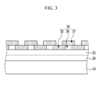
- FIG. 3 is a schematic cross-sectional view of the OLED display according to the exemplary embodiment.
- the flexible OLED display may include the thin film encapsulation layer 30 above an organic light emitting diode (OLED) layer 20.
- OLED organic light emitting diode
- the thin film encapsulation layer 30 includes a plurality of laminated inorganic layers 35 and 37, at least one of the plurality of inorganic layers 35 and 37 includes a plurality of inorganic layer patterns that are disposed to be spaced apart from each other on a plane, and an organic layer 36 may be formed between the plurality of inorganic layer patterns.
- the thin film encapsulation layer 30 covering the OLED layer 20 prevents (or blocks) external oxygen and moisture from flowing into the OLED to protect it.
- Each inorganic layer may be a single layer or laminated layers (stacked in a thickness direction) including a metal oxide or a metal nitride.
- the inorganic layer may be formed of a ceramic material such as a SiNx, a SiOx, a SiOxNy, etc., and/or may be formed of a transparent material such as AI2O3, TiO2, MgO, CrO, etc.
- the organic layer may be formed of a polymer, and may be, for example, a single layer or laminated layers formed of any one of polyethylene terephthalate, polyimide, polycarbonate, epoxy, polyethylene, and polyacrylate.
- a functional layer 25 may be further provided between the OLED layer 20 and the thin film encapsulation layer 30, and the functional layer 25 may be further included as a capping layer for protecting the OLED layer 20 or controlling light efficiency, and/or as a lithium fluoride (LiF) layer for preventing plasma damage by ions and/or controlling light efficiency.
- LiF lithium fluoride
- a halogenated metal layer including lithium fluoride may prevent or protect the organic emission layer from being damaged when the inorganic layers 35 and 37 are formed using (utilizing) a sputtering method and/or a plasma deposition method.
- the thin film encapsulation layer 30 includes a first inorganic layer 35 provided above the OLED layer 20 and including a plurality of first inorganic layer patterns 35' that are disposed to be spaced apart from each other, a first organic layer 36 disposed between the plurality of first inorganic layer patterns 35', and a second inorganic layer 37 disposed on the first organic layer 36 and including a plurality of second inorganic layer patterns 37' that are disposed to be spaced apart from each other.
- the thin film encapsulation layer 30 may consist of two inorganic layers 35 and 37 and one organic layer 36.
- the organic layer 36 may be formed by filling an organic material such as an epoxy, an acryl, a PI-based material, etc. between the first inorganic layer patterns 35'.
- first and second inorganic layer patterns 35' and 37' may be disposed above the organic emission layer of the OLED layer, that is, in a display area.
- FIG. 6 is a schematic top plan view of the thin film encapsulation layer of FIG. 3 .
- the first and second inorganic layer patterns 35' and 37' may partially contact each other in vertical and horizontal directions.
- edge portions of the first and second inorganic layer patterns 35' and 37' contact each other in the vertical direction (thickness direction) and partially overlap each other in the horizontal direction.
- the first and second inorganic layer patterns 35' and 37' are configured such that they are coupled to each other through the inorganic layer patterns of the inorganic layers of the respective different layers.
- the inorganic layer consisting of two layers is exemplarily illustrated, but an inorganic layer consisting of three or more layers may be possible.
- first and second inorganic layer patterns 35' and 37' may be formed as a matrix form in which an overall square shape (e.g., a square hexahedrical) is repeatedly disposed on a plane.
- an overall square shape e.g., a square hexahedrical
- the flexible substrate 10 may include a flexible plastic material, but is not limited thereto.
- the flexible substrate 10 may include a metallic substrate formed of stainless steel or the like, or various flexible materials may be used (utilized).
- the flexible substrate 10 may include a plastic material with excellent thermal resistance and durability such as polyethylene ether phthalate, polyethylene naphthalate, polycarbonate, polyarylate, polyetherimide, polyether sulfone, polyimide, etc.
- FIG. 4 is a schematic cross-sectional view of one example of the substrate according to the present invention.
- the substrate 10 includes, below a low temperature polysilicon (LTPS) layer 9, inorganic barrier layers 7 and 8, organic layers (e.g., polyimide layers) 3 and 6, and an amorphous silicon layer 5.
- LTPS low temperature polysilicon
- inorganic barrier layers 7 and 8 organic layers (e.g., polyimide layers) 3 and 6, and an amorphous silicon layer 5.
- the OLED layer 20 may be formed on the LTPS layer 9, and the inorganic layers such as SiNx and SiOx may be formed as the barrier layers 7 and 8.
- the organic layer 6 such as polyimide, the amorphous silicon layer 5, a SiOx layer 4, and the polyimide layer 3 may be sequentially downwardly laminated (i.e., downwardly stacked in a thickness direction).
- a lower protection film 2 may be attached to a bottom of the polyimide layer 3.
- FIG. 5 is a schematic cross-sectional view of a thin film encapsulation layer according to a further exemplary embodiment
- FIG. 7 is a schematic top plan view of the thin film encapsulation layer of FIG. 5 .
- a second organic layer 38 and a third inorganic layer 39 may be further included in the thin film encapsulation layer structure of FIG. 3 .
- the second organic layer 38 is disposed between the plurality of second inorganic layer patterns 37', and the third inorganic layer 39 may include a plurality of third inorganic layer patterns 39' that are disposed on the second organic layer 38 and between the second inorganic layer patterns 37' to be spaced apart from each other.
- the second and third inorganic layer patterns 37' and 39' may partially contact each other in vertical and horizontal structures.
- the second and third inorganic layer patterns 37' and 39' may be formed in a matrix form in which overall square shapes are repeatedly disposed on a plane.
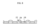
- FIG. 8 is a schematic cross-sectional view of a thin film encapsulation layer according to a further exemplary embodiment
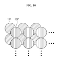
- FIG. 10 is a schematic top plan view of the thin film encapsulation layer of FIG. 8 .
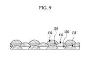
- first inorganic layer patterns 135' and second inorganic layer patterns 137' may be formed in a matrix form in which a circular shape (e.g., a circular semispherical shape) is repeatedly disposed on a plane.
- a circular shape e.g., a circular semispherical shape
- first and second inorganic layer patterns 135' and 137' may have a substantially semicircular shape in a vertical direction (thickness direction).
- first and second inorganic layer patterns 135' and 137' may partially contact each other and may be formed in a matrix form in which they are repeatedly disposed on a plane.
- FIGS. 9 and 11 are drawings schematically showing the thin film encapsulation layer structure in which a third inorganic layer with third inorganic layer patterns 139' are further included in the structure of FIGS. 8 and 10 .
- a second organic layer 138 and a third inorganic layer 139 may be further included in the thin film encapsulation layer structure of FIG. 8 .
- the second organic layer 138 is disposed between the plurality of second inorganic layer patterns 137', and the third inorganic layer 139 may include the plurality of third inorganic layer patterns 139' that are disposed on the second organic layer 138 and between the second inorganic layer patterns 137' to be spaced apart from each other.
- the second and third inorganic layer patterns 137' and 139' may partially contact each other, and may be formed in a matrix form in which they are repeatedly disposed on a plane.
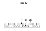
- FIG. 12 is a schematic cross-sectional view of a thin film encapsulation layer according to a further exemplary embodiment
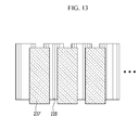
- FIG. 13 is a schematic top plan view of the thin film encapsulation layer of FIG. 12 .
- the thin film encapsulation layer may include: a first inorganic layer 235 including a plurality of first inorganic layer patterns 235' that are disposed to be spaced apart from each other; a first organic layer 236 disposed between a plurality of first inorganic layer patterns 235'; and a second inorganic layer 237 disposed on the first organic layer 236 and including a plurality of second inorganic layer patterns 237' that are disposed between the first inorganic layer patterns 235' to be spaced apart from each other.
- the first and second inorganic layer patterns 235' and 237' may be formed in a matrix form in which a rectangular shape (e.g., a rectangular hexahedrical) is repeatedly disposed on a plane.
- a rectangular shape e.g., a rectangular hexahedrical
- the plurality of first and second inorganic layer patterns 235' and 237' may be arranged in a direction along which the substrate 10 is bendable.
- the inorganic layer patterns 235' and 237' are repeatedly disposed on the plane in a horizontal direction, cracks of the inorganic layers of the thin film encapsulation layer can be prevented or reduced when the flexible OLED display is bent or folded in the horizontal direction.
- first and second inorganic layer patterns 235' and 237' may partially contact each other in vertical and horizontal directions.
- a second organic layer and a third inorganic layer may be further included in the thin film encapsulation layer structure of FIG. 12 .
- the second organic layer is disposed between a plurality of second inorganic layer patterns
- the third inorganic layer may include a plurality of third inorganic layer patterns that are disposed on the second organic layer and between the second inorganic layer patterns to be spaced apart from each other.
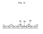
- FIG. 14 is a schematic cross-sectional view of a thin film encapsulation layer according to a further exemplary embodiment
- FIG. 15 is a schematic top plan view of the thin film encapsulation layer of FIG. 14 .
- the thin film encapsulation layer structure is similar to those of the aforementioned exemplary embodiments, but is different in that shapes of first and second inorganic layer patterns 335' and 337' may have a triangular pyramidal shape. Since the first and second inorganic layer patterns 335' and 337' may partially contact each other in vertical and horizontal structures, they may have an isosceles triangular shape in the vertical direction and may be formed as a matrix form on a plane in which an overall square shape is repeatedly disposed in the horizontal direction.
- the thin film encapsulation layer may further include a second organic layer 338 and a third inorganic layer 339 in the thin film encapsulation layer structure of FIG. 14 .
- the second organic layer 338 is disposed between the plurality of second inorganic layer patterns 337', and the third inorganic layer 339 includes a plurality of third inorganic layer patterns 339' that are disposed on the second organic layer 338 and between the second inorganic layer patterns 337' to be spaced apart from each other.
- the second and third inorganic layer patterns 337' and 339' may partially contact each other, and may be formed as a matrix form in which they are repeatedly disposed on a plane.
- Shapes of the inorganic layer patterns are not limited to square, rectangular, circular, and triangular pyramidal shapes according to the exemplary embodiments, and may be formed to have various other shapes.
- FIG. 18 is a schematic cross-sectional view of a thin film encapsulation layer according to a further exemplary embodiment.
- the flexible substrate 10 may be differentiated into a bending region B that is bendable and an unbending region A that is not bendable.
- the thin film encapsulation layer includes a first inorganic layer 435 provided above the OLED layer and including a plurality of first inorganic layer patterns 435' that are disposed to be spaced apart from each other, a first organic layer 436 disposed between the plurality of first inorganic layer patterns 435', and a second inorganic layer 437 disposed on the first organic layer 436 and including a plurality of second inorganic layer patterns 437' that are disposed between the first inorganic layer patterns 435' to be spaced apart from each other.
- sizes of the first and second inorganic layer patterns 435' and 437' may be reduced in a bending region B, and the sizes of the first and second inorganic layer patterns 435' and 437' may be increased in an unbending region A. That in, the first and second inorganic layer patterns 435' and 437' in the bending region B may be smaller in size than that of the first and second inorganic layer patterns 435' and 437' in the unbending region A.
- the sizes of the inorganic layer patterns 435' and 437' are reduced such that a large number of the inorganic layer patterns 435' and 437' are formed in a unit area, thereby further reducing propagation of shocks and cracks caused by the generated stress.
- the bending region B may be a non-active area, and the unbending region A may be an active area.
- the bending region and the unbending region are not strictly differentiated, and the sizes of the inorganic layer patterns 435' and 437' and the number thereof per unit area can be controlled as necessary.
- a manufacturing method of a flexible OLED display includes, on a substrate, forming an OLED layer including an anode coupled to a transistor, an organic emission layer formed on the anode, and a cathode formed on the organic emission layer, and forming a thin film encapsulation layer on the organic light emitting diode layer.
- the forming of the thin film encapsulation layer may include: a first deposition act of depositing a first inorganic layer on the OLED layer; a first etching act of patterning the first inorganic layer to include a plurality of first inorganic layer patterns that are disposed to be spaced apart from each other; a second deposition act of depositing a first organic layer between the patterned first inorganic layer patterns utilizing a first mask; a third deposition act of depositing a second inorganic layer on the first organic layer; and a second etching act of patterning the second inorganic layer to include a plurality of second inorganic layer patterns that are disposed to be spaced apart from each other.
- the manufacturing method may further include: a fourth deposition act of depositing a second organic layer between the patterned second inorganic layer patterns utilizing a second mask; a fifth deposition act of depositing a third inorganic layer on the second organic layer; and a third etching act of patterning the third inorganic layer to include a plurality of third inorganic layer patterns that are disposed to be spaced apart from each other.
- the manufacturing method may further include forming a capping layer for protecting the cathode or controlling light efficiency on the cathode.
- the manufacturing method may further include forming a lithium fluoride (LiF) layer for preventing plasma damage by ions and/or controlling light efficiency on the cathode.
- LiF lithium fluoride
- the stress of the inorganic layers is alleviated by the inorganic layer patterns of the inorganic layers of the thin film encapsulation layer, thereby preventing or reducing the cracks generated at the inorganic layer and/or the moisture permeation into the display area from the thin film encapsulation layer.
- substrate 20 organic light emitting diode layer 30: thin film encapsulation layer 35: first inorganic layer 36: first organic layer 37: second inorganic layer 38: second organic layer 39: third inorganic layer 35': first inorganic layer pattern 37': second inorganic layer pattern 39': third inorganic layer pattern
Landscapes
- Chemical & Material Sciences (AREA)
- Inorganic Chemistry (AREA)
- Physics & Mathematics (AREA)
- Optics & Photonics (AREA)
- Engineering & Computer Science (AREA)
- Manufacturing & Machinery (AREA)
- Electroluminescent Light Sources (AREA)
Applications Claiming Priority (2)
| Application Number | Priority Date | Filing Date | Title |
|---|---|---|---|
| KR20130122869 | 2013-10-15 | ||
| KR1020140125183A KR102271586B1 (ko) | 2013-10-15 | 2014-09-19 | 가요성 유기 발광 표시 장치 및 그 제조 방법 |
Publications (3)
| Publication Number | Publication Date |
|---|---|
| EP2863446A2 true EP2863446A2 (de) | 2015-04-22 |
| EP2863446A3 EP2863446A3 (de) | 2015-05-13 |
| EP2863446B1 EP2863446B1 (de) | 2017-02-01 |
Family
ID=51726389
Family Applications (1)
| Application Number | Title | Priority Date | Filing Date |
|---|---|---|---|
| EP14188721.6A Not-in-force EP2863446B1 (de) | 2013-10-15 | 2014-10-14 | Flexible organische lichtemittierende Diodenanzeige und Herstellungsverfahren dafür |
Country Status (2)
| Country | Link |
|---|---|
| US (1) | US9293730B2 (de) |
| EP (1) | EP2863446B1 (de) |
Families Citing this family (19)
| Publication number | Priority date | Publication date | Assignee | Title |
|---|---|---|---|---|
| CN105788459A (zh) * | 2015-08-19 | 2016-07-20 | 广州奥翼电子科技有限公司 | 柔性显示器及其制备方法 |
| KR102339282B1 (ko) | 2015-11-02 | 2021-12-15 | 삼성디스플레이 주식회사 | 디스플레이 장치 |
| US10361385B2 (en) | 2016-02-12 | 2019-07-23 | Samsung Display Co., Ltd. | Display device |
| KR102505879B1 (ko) | 2016-03-24 | 2023-03-06 | 삼성디스플레이 주식회사 | 디스플레이 장치 |
| JP6783573B2 (ja) | 2016-07-22 | 2020-11-11 | 株式会社ジャパンディスプレイ | 表示装置 |
| CN106206994B (zh) | 2016-09-26 | 2019-04-26 | 京东方科技集团股份有限公司 | 一种显示面板及制备方法 |
| CN106328810B (zh) * | 2016-10-17 | 2019-03-12 | 武汉华星光电技术有限公司 | 柔性oled基板结构和设计方法 |
| KR102729880B1 (ko) * | 2016-10-31 | 2024-11-13 | 엘지디스플레이 주식회사 | 유기 발광 표시 장치 |
| CN106848106B (zh) | 2017-04-19 | 2019-03-29 | 京东方科技集团股份有限公司 | 有机电致发光装置封装结构及其制作方法、显示装置 |
| CN107154422B (zh) | 2017-05-12 | 2019-11-15 | 武汉华星光电技术有限公司 | 一种柔性有机发光二极管显示器及其制作方法 |
| CN107482127A (zh) * | 2017-07-25 | 2017-12-15 | 武汉华星光电半导体显示技术有限公司 | Oled柔性显示面板及其制作方法 |
| CN107492601A (zh) * | 2017-09-30 | 2017-12-19 | 京东方科技集团股份有限公司 | 一种显示器件及其封装方法、显示装置 |
| US10490758B2 (en) * | 2017-10-30 | 2019-11-26 | Wuhan China Star Optoelectronics Semiconductor Display Technology Co., Ltd. | Flexible OLED display panel and manufacturing method thereof |
| EP3776681B1 (de) | 2018-03-30 | 2025-10-08 | BOE Technology Group Co., Ltd. | Organische lichtemittierende diodenanzeigetafel und anzeigevorrichtung sowie herstellungsverfahren dafür |
| CN108305892B (zh) * | 2018-04-03 | 2024-05-24 | 京东方科技集团股份有限公司 | 一种柔性衬底基板及其制备方法、显示装置 |
| CN109065760B (zh) * | 2018-08-22 | 2021-04-27 | 京东方科技集团股份有限公司 | 封装结构及封装方法、显示装置 |
| US11036320B2 (en) * | 2019-01-30 | 2021-06-15 | Wuhan China Star Optoelectronics Semiconductor Display Technology Co., Ltd. | Organic light emitting diode folding display |
| CN109873090B (zh) | 2019-03-29 | 2021-10-29 | 合肥鑫晟光电科技有限公司 | 封装结构、显示基板、显示装置及显示器件的封装方法 |
| CN213814635U (zh) * | 2021-01-25 | 2021-07-27 | 合肥维信诺科技有限公司 | 触控面板、显示面板以及显示装置 |
Family Cites Families (24)
| Publication number | Priority date | Publication date | Assignee | Title |
|---|---|---|---|---|
| US5686360A (en) | 1995-11-30 | 1997-11-11 | Motorola | Passivation of organic devices |
| US20070196682A1 (en) | 1999-10-25 | 2007-08-23 | Visser Robert J | Three dimensional multilayer barrier and method of making |
| KR100695169B1 (ko) * | 2006-01-11 | 2007-03-14 | 삼성전자주식회사 | 평판표시장치 |
| KR100647339B1 (ko) * | 2006-01-11 | 2006-11-23 | 삼성전자주식회사 | 평판표시장치 |
| KR100707210B1 (ko) | 2006-02-03 | 2007-04-13 | 삼성전자주식회사 | 유기발광 디스플레이 및 그 제조방법 |
| KR100682963B1 (ko) * | 2006-02-03 | 2007-02-15 | 삼성전자주식회사 | 자외선 차단막을 구비한 유기발광 디스플레이 |
| JP4763496B2 (ja) | 2006-03-30 | 2011-08-31 | 株式会社巴川製紙所 | 薄膜およびそれを用いた薄膜積層体 |
| KR20080088750A (ko) * | 2007-03-30 | 2008-10-06 | 삼성전자주식회사 | 유기발광장치 및 그 제조방법 |
| KR20080107834A (ko) | 2007-06-08 | 2008-12-11 | 삼성전자주식회사 | 종이기판 제조방법 및 이를 이용한 표시소자 |
| JP2009188223A (ja) | 2008-02-07 | 2009-08-20 | Seiko Instruments Inc | 半導体装置 |
| EP2151876A1 (de) * | 2008-08-05 | 2010-02-10 | Nederlandse Organisatie voor toegepast- natuurwetenschappelijk onderzoek TNO | Elektrische Transportkomponente, Herstellungsverfahren dafür sowie elektro-optische Vorrichtung und opto-elektrische Vorrichtung |
| KR100994121B1 (ko) * | 2009-03-11 | 2010-11-15 | 삼성모바일디스플레이주식회사 | 유기 발광 표시 장치 |
| JP5290078B2 (ja) | 2009-07-22 | 2013-09-18 | 株式会社ジャパンディスプレイ | フレキシブル表示装置 |
| KR101065318B1 (ko) | 2009-12-03 | 2011-09-16 | 삼성모바일디스플레이주식회사 | 플렉서블 디스플레이 장치의 제조 방법 |
| KR101097321B1 (ko) | 2009-12-14 | 2011-12-23 | 삼성모바일디스플레이주식회사 | 유기 발광 장치 및 이의 제조 방법 |
| KR101155904B1 (ko) | 2010-01-04 | 2012-06-20 | 삼성모바일디스플레이주식회사 | 유기 발광 표시 장치 |
| KR101430173B1 (ko) * | 2010-10-19 | 2014-08-13 | 삼성디스플레이 주식회사 | 유기 발광 표시 장치 |
| EP2445028A1 (de) | 2010-10-25 | 2012-04-25 | Nederlandse Organisatie voor toegepast -natuurwetenschappelijk onderzoek TNO | Optoelektrische Vorrichtung und Verfahren zur Herstellung einer optoelektrischen Vorrichtung |
| JP2012204103A (ja) * | 2011-03-24 | 2012-10-22 | Toshiba Corp | 有機電界発光素子、表示装置および照明装置 |
| KR101407310B1 (ko) * | 2011-12-30 | 2014-06-16 | 엘지디스플레이 주식회사 | 유기 발광 표시 장치 및 이의 제조 방법 |
| KR101972077B1 (ko) | 2012-09-28 | 2019-08-19 | 삼성디스플레이 주식회사 | 유기 발광 표시 장치 |
| TWI492374B (zh) * | 2012-12-03 | 2015-07-11 | Au Optronics Corp | 電激發光顯示面板 |
| CN103022354B (zh) | 2012-12-28 | 2016-05-11 | 昆山工研院新型平板显示技术中心有限公司 | 一种柔性衬底 |
| KR20140106844A (ko) * | 2013-02-27 | 2014-09-04 | 노재상 | 산화 그래핀 또는 환원된 산화 그래핀으로 이루어진 박편층을 포함하는 봉지막 및 그의 형성 방법 |
-
2014
- 2014-10-08 US US14/510,064 patent/US9293730B2/en not_active Expired - Fee Related
- 2014-10-14 EP EP14188721.6A patent/EP2863446B1/de not_active Not-in-force
Non-Patent Citations (1)
| Title |
|---|
| None |
Also Published As
| Publication number | Publication date |
|---|---|
| US9293730B2 (en) | 2016-03-22 |
| US20150102326A1 (en) | 2015-04-16 |
| EP2863446B1 (de) | 2017-02-01 |
| EP2863446A3 (de) | 2015-05-13 |
Similar Documents
| Publication | Publication Date | Title |
|---|---|---|
| US9293730B2 (en) | Flexible organic light emitting diode display and manufacturing method thereof | |
| KR102271586B1 (ko) | 가요성 유기 발광 표시 장치 및 그 제조 방법 | |
| US10976853B2 (en) | Display device | |
| KR102111562B1 (ko) | 표시 장치 | |
| CN112799550B (zh) | 一种触控显示面板及触控显示装置 | |
| CN112667106B (zh) | 一种触控显示面板及触控显示装置 | |
| US11690265B2 (en) | Display device having a trench portion | |
| KR102615113B1 (ko) | 플렉서블 디스플레이 장치 | |
| US9000428B2 (en) | Organic light emitting diode display | |
| EP3131132B1 (de) | Anzeigevorrichtung und verfahren zur herstellung einer anzeigevorrichtung | |
| KR101984736B1 (ko) | 플렉서블 디스플레이 장치용 어레이 기판 | |
| CN103811675B (zh) | 柔性有机电致发光装置及其制造方法 | |
| EP2747062A2 (de) | Organische lichtemittierende Diodenanzeige | |
| KR20200145952A (ko) | 표시 장치 | |
| US11411060B2 (en) | Organic light-emitting display device having multiple wirings and an encapsulation layer including stacked layers | |
| KR20140143637A (ko) | 가요성 표시 장치 및 그 제조방법 | |
| KR20150085668A (ko) | 디스플레이 장치 | |
| KR102000716B1 (ko) | 유기 발광 표시 장치 및 이의 제조 방법 | |
| CN105810716A (zh) | 柔性显示装置及制备方法 | |
| CN111697030A (zh) | 显示装置 | |
| US9536936B2 (en) | Organic light emitting diode display | |
| KR102147846B1 (ko) | 유기 발광 표시 장치 |
Legal Events
| Date | Code | Title | Description |
|---|---|---|---|
| PUAL | Search report despatched |
Free format text: ORIGINAL CODE: 0009013 |
|
| PUAI | Public reference made under article 153(3) epc to a published international application that has entered the european phase |
Free format text: ORIGINAL CODE: 0009012 |
|
| 17P | Request for examination filed |
Effective date: 20141014 |
|
| AK | Designated contracting states |
Kind code of ref document: A2 Designated state(s): AL AT BE BG CH CY CZ DE DK EE ES FI FR GB GR HR HU IE IS IT LI LT LU LV MC MK MT NL NO PL PT RO RS SE SI SK SM TR |
|
| AX | Request for extension of the european patent |
Extension state: BA ME |
|
| AK | Designated contracting states |
Kind code of ref document: A3 Designated state(s): AL AT BE BG CH CY CZ DE DK EE ES FI FR GB GR HR HU IE IS IT LI LT LU LV MC MK MT NL NO PL PT RO RS SE SI SK SM TR |
|
| AX | Request for extension of the european patent |
Extension state: BA ME |
|
| RIC1 | Information provided on ipc code assigned before grant |
Ipc: H01L 51/52 20060101AFI20150408BHEP Ipc: H01L 27/32 20060101ALI20150408BHEP |
|
| R17P | Request for examination filed (corrected) |
Effective date: 20150713 |
|
| RBV | Designated contracting states (corrected) |
Designated state(s): AL AT BE BG CH CY CZ DE DK EE ES FI FR GB GR HR HU IE IS IT LI LT LU LV MC MK MT NL NO PL PT RO RS SE SI SK SM TR |
|
| RAP1 | Party data changed (applicant data changed or rights of an application transferred) |
Owner name: SAMSUNG DISPLAY CO., LTD. |
|
| GRAP | Despatch of communication of intention to grant a patent |
Free format text: ORIGINAL CODE: EPIDOSNIGR1 |
|
| INTG | Intention to grant announced |
Effective date: 20160906 |
|
| GRAS | Grant fee paid |
Free format text: ORIGINAL CODE: EPIDOSNIGR3 |
|
| STAA | Information on the status of an ep patent application or granted ep patent |
Free format text: STATUS: GRANT OF PATENT IS INTENDED |
|
| GRAA | (expected) grant |
Free format text: ORIGINAL CODE: 0009210 |
|
| STAA | Information on the status of an ep patent application or granted ep patent |
Free format text: STATUS: THE PATENT HAS BEEN GRANTED |
|
| AK | Designated contracting states |
Kind code of ref document: B1 Designated state(s): AL AT BE BG CH CY CZ DE DK EE ES FI FR GB GR HR HU IE IS IT LI LT LU LV MC MK MT NL NO PL PT RO RS SE SI SK SM TR |
|
| REG | Reference to a national code |
Ref country code: GB Ref legal event code: FG4D |
|
| REG | Reference to a national code |
Ref country code: CH Ref legal event code: EP Ref country code: AT Ref legal event code: REF Ref document number: 866227 Country of ref document: AT Kind code of ref document: T Effective date: 20170215 |
|
| REG | Reference to a national code |
Ref country code: IE Ref legal event code: FG4D |
|
| REG | Reference to a national code |
Ref country code: DE Ref legal event code: R096 Ref document number: 602014006516 Country of ref document: DE |
|
| REG | Reference to a national code |
Ref country code: NL Ref legal event code: FP |
|
| REG | Reference to a national code |
Ref country code: LT Ref legal event code: MG4D |
|
| REG | Reference to a national code |
Ref country code: AT Ref legal event code: MK05 Ref document number: 866227 Country of ref document: AT Kind code of ref document: T Effective date: 20170201 |
|
| PG25 | Lapsed in a contracting state [announced via postgrant information from national office to epo] |
Ref country code: IS Free format text: LAPSE BECAUSE OF FAILURE TO SUBMIT A TRANSLATION OF THE DESCRIPTION OR TO PAY THE FEE WITHIN THE PRESCRIBED TIME-LIMIT Effective date: 20170601 Ref country code: LT Free format text: LAPSE BECAUSE OF FAILURE TO SUBMIT A TRANSLATION OF THE DESCRIPTION OR TO PAY THE FEE WITHIN THE PRESCRIBED TIME-LIMIT Effective date: 20170201 Ref country code: FI Free format text: LAPSE BECAUSE OF FAILURE TO SUBMIT A TRANSLATION OF THE DESCRIPTION OR TO PAY THE FEE WITHIN THE PRESCRIBED TIME-LIMIT Effective date: 20170201 Ref country code: GR Free format text: LAPSE BECAUSE OF FAILURE TO SUBMIT A TRANSLATION OF THE DESCRIPTION OR TO PAY THE FEE WITHIN THE PRESCRIBED TIME-LIMIT Effective date: 20170502 Ref country code: NO Free format text: LAPSE BECAUSE OF FAILURE TO SUBMIT A TRANSLATION OF THE DESCRIPTION OR TO PAY THE FEE WITHIN THE PRESCRIBED TIME-LIMIT Effective date: 20170501 Ref country code: HR Free format text: LAPSE BECAUSE OF FAILURE TO SUBMIT A TRANSLATION OF THE DESCRIPTION OR TO PAY THE FEE WITHIN THE PRESCRIBED TIME-LIMIT Effective date: 20170201 |
|
| PG25 | Lapsed in a contracting state [announced via postgrant information from national office to epo] |
Ref country code: LV Free format text: LAPSE BECAUSE OF FAILURE TO SUBMIT A TRANSLATION OF THE DESCRIPTION OR TO PAY THE FEE WITHIN THE PRESCRIBED TIME-LIMIT Effective date: 20170201 Ref country code: PT Free format text: LAPSE BECAUSE OF FAILURE TO SUBMIT A TRANSLATION OF THE DESCRIPTION OR TO PAY THE FEE WITHIN THE PRESCRIBED TIME-LIMIT Effective date: 20170601 Ref country code: BG Free format text: LAPSE BECAUSE OF FAILURE TO SUBMIT A TRANSLATION OF THE DESCRIPTION OR TO PAY THE FEE WITHIN THE PRESCRIBED TIME-LIMIT Effective date: 20170501 Ref country code: RS Free format text: LAPSE BECAUSE OF FAILURE TO SUBMIT A TRANSLATION OF THE DESCRIPTION OR TO PAY THE FEE WITHIN THE PRESCRIBED TIME-LIMIT Effective date: 20170201 Ref country code: PL Free format text: LAPSE BECAUSE OF FAILURE TO SUBMIT A TRANSLATION OF THE DESCRIPTION OR TO PAY THE FEE WITHIN THE PRESCRIBED TIME-LIMIT Effective date: 20170201 Ref country code: ES Free format text: LAPSE BECAUSE OF FAILURE TO SUBMIT A TRANSLATION OF THE DESCRIPTION OR TO PAY THE FEE WITHIN THE PRESCRIBED TIME-LIMIT Effective date: 20170201 Ref country code: SE Free format text: LAPSE BECAUSE OF FAILURE TO SUBMIT A TRANSLATION OF THE DESCRIPTION OR TO PAY THE FEE WITHIN THE PRESCRIBED TIME-LIMIT Effective date: 20170201 Ref country code: AT Free format text: LAPSE BECAUSE OF FAILURE TO SUBMIT A TRANSLATION OF THE DESCRIPTION OR TO PAY THE FEE WITHIN THE PRESCRIBED TIME-LIMIT Effective date: 20170201 |
|
| REG | Reference to a national code |
Ref country code: FR Ref legal event code: PLFP Year of fee payment: 4 |
|
| PG25 | Lapsed in a contracting state [announced via postgrant information from national office to epo] |
Ref country code: IT Free format text: LAPSE BECAUSE OF FAILURE TO SUBMIT A TRANSLATION OF THE DESCRIPTION OR TO PAY THE FEE WITHIN THE PRESCRIBED TIME-LIMIT Effective date: 20170201 Ref country code: SK Free format text: LAPSE BECAUSE OF FAILURE TO SUBMIT A TRANSLATION OF THE DESCRIPTION OR TO PAY THE FEE WITHIN THE PRESCRIBED TIME-LIMIT Effective date: 20170201 Ref country code: RO Free format text: LAPSE BECAUSE OF FAILURE TO SUBMIT A TRANSLATION OF THE DESCRIPTION OR TO PAY THE FEE WITHIN THE PRESCRIBED TIME-LIMIT Effective date: 20170201 Ref country code: CZ Free format text: LAPSE BECAUSE OF FAILURE TO SUBMIT A TRANSLATION OF THE DESCRIPTION OR TO PAY THE FEE WITHIN THE PRESCRIBED TIME-LIMIT Effective date: 20170201 Ref country code: EE Free format text: LAPSE BECAUSE OF FAILURE TO SUBMIT A TRANSLATION OF THE DESCRIPTION OR TO PAY THE FEE WITHIN THE PRESCRIBED TIME-LIMIT Effective date: 20170201 |
|
| REG | Reference to a national code |
Ref country code: DE Ref legal event code: R097 Ref document number: 602014006516 Country of ref document: DE |
|
| PG25 | Lapsed in a contracting state [announced via postgrant information from national office to epo] |
Ref country code: DK Free format text: LAPSE BECAUSE OF FAILURE TO SUBMIT A TRANSLATION OF THE DESCRIPTION OR TO PAY THE FEE WITHIN THE PRESCRIBED TIME-LIMIT Effective date: 20170201 Ref country code: SM Free format text: LAPSE BECAUSE OF FAILURE TO SUBMIT A TRANSLATION OF THE DESCRIPTION OR TO PAY THE FEE WITHIN THE PRESCRIBED TIME-LIMIT Effective date: 20170201 |
|
| PLBE | No opposition filed within time limit |
Free format text: ORIGINAL CODE: 0009261 |
|
| STAA | Information on the status of an ep patent application or granted ep patent |
Free format text: STATUS: NO OPPOSITION FILED WITHIN TIME LIMIT |
|
| 26N | No opposition filed |
Effective date: 20171103 |
|
| PG25 | Lapsed in a contracting state [announced via postgrant information from national office to epo] |
Ref country code: SI Free format text: LAPSE BECAUSE OF FAILURE TO SUBMIT A TRANSLATION OF THE DESCRIPTION OR TO PAY THE FEE WITHIN THE PRESCRIBED TIME-LIMIT Effective date: 20170201 |
|
| PG25 | Lapsed in a contracting state [announced via postgrant information from national office to epo] |
Ref country code: MC Free format text: LAPSE BECAUSE OF FAILURE TO SUBMIT A TRANSLATION OF THE DESCRIPTION OR TO PAY THE FEE WITHIN THE PRESCRIBED TIME-LIMIT Effective date: 20170201 |
|
| REG | Reference to a national code |
Ref country code: CH Ref legal event code: PL |
|
| REG | Reference to a national code |
Ref country code: IE Ref legal event code: MM4A |
|
| PG25 | Lapsed in a contracting state [announced via postgrant information from national office to epo] |
Ref country code: CH Free format text: LAPSE BECAUSE OF NON-PAYMENT OF DUE FEES Effective date: 20171031 Ref country code: LU Free format text: LAPSE BECAUSE OF NON-PAYMENT OF DUE FEES Effective date: 20171014 Ref country code: LI Free format text: LAPSE BECAUSE OF NON-PAYMENT OF DUE FEES Effective date: 20171031 |
|
| REG | Reference to a national code |
Ref country code: BE Ref legal event code: MM Effective date: 20171031 |
|
| PG25 | Lapsed in a contracting state [announced via postgrant information from national office to epo] |
Ref country code: BE Free format text: LAPSE BECAUSE OF NON-PAYMENT OF DUE FEES Effective date: 20171031 |
|
| REG | Reference to a national code |
Ref country code: FR Ref legal event code: PLFP Year of fee payment: 5 |
|
| PG25 | Lapsed in a contracting state [announced via postgrant information from national office to epo] |
Ref country code: MT Free format text: LAPSE BECAUSE OF NON-PAYMENT OF DUE FEES Effective date: 20171014 |
|
| PG25 | Lapsed in a contracting state [announced via postgrant information from national office to epo] |
Ref country code: IE Free format text: LAPSE BECAUSE OF NON-PAYMENT OF DUE FEES Effective date: 20171014 |
|
| PG25 | Lapsed in a contracting state [announced via postgrant information from national office to epo] |
Ref country code: HU Free format text: LAPSE BECAUSE OF FAILURE TO SUBMIT A TRANSLATION OF THE DESCRIPTION OR TO PAY THE FEE WITHIN THE PRESCRIBED TIME-LIMIT; INVALID AB INITIO Effective date: 20141014 |
|
| PG25 | Lapsed in a contracting state [announced via postgrant information from national office to epo] |
Ref country code: CY Free format text: LAPSE BECAUSE OF FAILURE TO SUBMIT A TRANSLATION OF THE DESCRIPTION OR TO PAY THE FEE WITHIN THE PRESCRIBED TIME-LIMIT Effective date: 20170201 |
|
| PG25 | Lapsed in a contracting state [announced via postgrant information from national office to epo] |
Ref country code: MK Free format text: LAPSE BECAUSE OF FAILURE TO SUBMIT A TRANSLATION OF THE DESCRIPTION OR TO PAY THE FEE WITHIN THE PRESCRIBED TIME-LIMIT Effective date: 20170201 |
|
| PG25 | Lapsed in a contracting state [announced via postgrant information from national office to epo] |
Ref country code: TR Free format text: LAPSE BECAUSE OF FAILURE TO SUBMIT A TRANSLATION OF THE DESCRIPTION OR TO PAY THE FEE WITHIN THE PRESCRIBED TIME-LIMIT Effective date: 20170201 |
|
| PG25 | Lapsed in a contracting state [announced via postgrant information from national office to epo] |
Ref country code: AL Free format text: LAPSE BECAUSE OF FAILURE TO SUBMIT A TRANSLATION OF THE DESCRIPTION OR TO PAY THE FEE WITHIN THE PRESCRIBED TIME-LIMIT Effective date: 20170201 |
|
| PGFP | Annual fee paid to national office [announced via postgrant information from national office to epo] |
Ref country code: NL Payment date: 20201008 Year of fee payment: 7 |
|
| PGFP | Annual fee paid to national office [announced via postgrant information from national office to epo] |
Ref country code: GB Payment date: 20201012 Year of fee payment: 7 Ref country code: DE Payment date: 20201006 Year of fee payment: 7 Ref country code: FR Payment date: 20201008 Year of fee payment: 7 |
|
| REG | Reference to a national code |
Ref country code: DE Ref legal event code: R119 Ref document number: 602014006516 Country of ref document: DE |
|
| REG | Reference to a national code |
Ref country code: NL Ref legal event code: MM Effective date: 20211101 |
|
| GBPC | Gb: european patent ceased through non-payment of renewal fee |
Effective date: 20211014 |
|
| PG25 | Lapsed in a contracting state [announced via postgrant information from national office to epo] |
Ref country code: NL Free format text: LAPSE BECAUSE OF NON-PAYMENT OF DUE FEES Effective date: 20211101 Ref country code: GB Free format text: LAPSE BECAUSE OF NON-PAYMENT OF DUE FEES Effective date: 20211014 Ref country code: DE Free format text: LAPSE BECAUSE OF NON-PAYMENT OF DUE FEES Effective date: 20220503 |
|
| PG25 | Lapsed in a contracting state [announced via postgrant information from national office to epo] |
Ref country code: FR Free format text: LAPSE BECAUSE OF NON-PAYMENT OF DUE FEES Effective date: 20211031 |