EP2853029B1 - Schaltungsanordnung und verfahren zum kalibrieren von ansteuersignalen für spannungsgesteuerte oszillatoren - Google Patents
Schaltungsanordnung und verfahren zum kalibrieren von ansteuersignalen für spannungsgesteuerte oszillatoren Download PDFInfo
- Publication number
- EP2853029B1 EP2853029B1 EP13756304.5A EP13756304A EP2853029B1 EP 2853029 B1 EP2853029 B1 EP 2853029B1 EP 13756304 A EP13756304 A EP 13756304A EP 2853029 B1 EP2853029 B1 EP 2853029B1
- Authority
- EP
- European Patent Office
- Prior art keywords
- vcm
- connection
- transistor
- varactor
- oscillator
- Prior art date
- Legal status (The legal status is an assumption and is not a legal conclusion. Google has not performed a legal analysis and makes no representation as to the accuracy of the status listed.)
- Active
Links
Images


Classifications
-
- H—ELECTRICITY
- H03—ELECTRONIC CIRCUITRY
- H03L—AUTOMATIC CONTROL, STARTING, SYNCHRONISATION OR STABILISATION OF GENERATORS OF ELECTRONIC OSCILLATIONS OR PULSES
- H03L7/00—Automatic control of frequency or phase; Synchronisation
-
- H—ELECTRICITY
- H03—ELECTRONIC CIRCUITRY
- H03L—AUTOMATIC CONTROL, STARTING, SYNCHRONISATION OR STABILISATION OF GENERATORS OF ELECTRONIC OSCILLATIONS OR PULSES
- H03L7/00—Automatic control of frequency or phase; Synchronisation
- H03L7/06—Automatic control of frequency or phase; Synchronisation using a reference signal applied to a frequency- or phase-locked loop
- H03L7/08—Details of the phase-locked loop
- H03L7/0805—Details of the phase-locked loop the loop being adapted to provide an additional control signal for use outside the loop
-
- H—ELECTRICITY
- H03—ELECTRONIC CIRCUITRY
- H03B—GENERATION OF OSCILLATIONS, DIRECTLY OR BY FREQUENCY-CHANGING, BY CIRCUITS EMPLOYING ACTIVE ELEMENTS WHICH OPERATE IN A NON-SWITCHING MANNER; GENERATION OF NOISE BY SUCH CIRCUITS
- H03B1/00—Details
-
- H—ELECTRICITY
- H03—ELECTRONIC CIRCUITRY
- H03L—AUTOMATIC CONTROL, STARTING, SYNCHRONISATION OR STABILISATION OF GENERATORS OF ELECTRONIC OSCILLATIONS OR PULSES
- H03L7/00—Automatic control of frequency or phase; Synchronisation
- H03L7/06—Automatic control of frequency or phase; Synchronisation using a reference signal applied to a frequency- or phase-locked loop
- H03L7/08—Details of the phase-locked loop
- H03L7/085—Details of the phase-locked loop concerning mainly the frequency- or phase-detection arrangement including the filtering or amplification of its output signal
-
- H—ELECTRICITY
- H03—ELECTRONIC CIRCUITRY
- H03L—AUTOMATIC CONTROL, STARTING, SYNCHRONISATION OR STABILISATION OF GENERATORS OF ELECTRONIC OSCILLATIONS OR PULSES
- H03L7/00—Automatic control of frequency or phase; Synchronisation
- H03L7/06—Automatic control of frequency or phase; Synchronisation using a reference signal applied to a frequency- or phase-locked loop
- H03L7/08—Details of the phase-locked loop
- H03L7/099—Details of the phase-locked loop concerning mainly the controlled oscillator of the loop
-
- H—ELECTRICITY
- H03—ELECTRONIC CIRCUITRY
- H03L—AUTOMATIC CONTROL, STARTING, SYNCHRONISATION OR STABILISATION OF GENERATORS OF ELECTRONIC OSCILLATIONS OR PULSES
- H03L7/00—Automatic control of frequency or phase; Synchronisation
- H03L7/06—Automatic control of frequency or phase; Synchronisation using a reference signal applied to a frequency- or phase-locked loop
- H03L7/16—Indirect frequency synthesis, i.e. generating a desired one of a number of predetermined frequencies using a frequency- or phase-locked loop
- H03L7/18—Indirect frequency synthesis, i.e. generating a desired one of a number of predetermined frequencies using a frequency- or phase-locked loop using a frequency divider or counter in the loop
-
- H—ELECTRICITY
- H04—ELECTRIC COMMUNICATION TECHNIQUE
- H04L—TRANSMISSION OF DIGITAL INFORMATION, e.g. TELEGRAPHIC COMMUNICATION
- H04L7/00—Arrangements for synchronising receiver with transmitter
- H04L7/02—Speed or phase control by the received code signals, the signals containing no special synchronisation information
- H04L7/033—Speed or phase control by the received code signals, the signals containing no special synchronisation information using the transitions of the received signal to control the phase of the synchronising-signal-generating means, e.g. using a phase-locked loop
Definitions
- CDR circuits with binary phase detectors are often used for data transmission in the frequency range greater than one gigahertz, because they are easier to implement at limited speed of the technology used and show a very robust behavior (better so-called power supply rejection).
- VCO Voltage Controlled Oscillator
- Fig. 1 shows a first example of a voltage-controlled ring oscillator RO with two tuning inputs Vtune1, Vtune2 from the prior art.
- the frequency of this voltage-controlled oscillator RO can be set separately via these two tuning inputs Vtune1 and Vtune2.
- the frequency change is set by four separate varactor (diodes) D1, D2, D3, D4.
- Fig. 2 shows a second example of a voltage-controlled ring oscillator RO 'with two tuning inputs Vtune1, Vtune2 from the prior art.
- up and dnb can be the digital output signals of a binary phase detector.
- the publication US Pat. No. 7,129,763 B1 discloses a digital circuitry for a computing device; in particular, the disclosure US Pat. No. 7,129,763 B1 adjusting the power consumption of the digital circuitry by generating a frequency error representing an error in a signal delay. Consequently, the US Pat. No. 7,129,763 B1 the goal is to reduce power consumption in a digital circuit. As a measure serve internal signal delays of the circuit, which must remain within acceptable limits.
- the present invention has the object, a circuit arrangement according to the preamble of claim 1 and a method according to the preamble of claim 13 educate so that the energy consumption as possible low and the output frequency is as large as possible.
- VCO Voltage-Controlled Oscillator
- CDR Clock and Data Recovery
- the at least one binary phase detector so-called Bang-Bang phase detector or up / Down phase detector
- a low power consumption that is, a low energy consumption feasible, because due to lower parasitic capacity than in the prior art less power is required to achieve the same output frequency.
- a higher output frequency is feasible, because only two varactors (instead of four varactors in the prior art) less parasitic capacitance is generated in the voltage controlled oscillator, so that the layout of the voltage controlled oscillator can be made more compact.
- VCO Voltage-Controlled Oscillator
- CDR clock and data recovery
- Fig. 4 shows an embodiment of a voltage-controlled ring oscillator 10.
- the frequency of this voltage-controlled oscillator 10 may - unlike in the prior art (see. Fig. 1 . Fig. 2 ), according to which two tuning inputs are required - are set via a calibrated drive signal Vbb.
- the frequency change is set by two varactor (diodes) or tuning diodes or varactor diodes or varicaps 12, 14.
- Fig. 4 can be seen that the anodic terminal of the first varactor 12 of the voltage controlled oscillator 10 and the anodic terminal of the second varactor 14 of the voltage controlled oscillator 10 are supplied with the calibrated drive signal Vbb.
- the cathodic terminal of the first varactor 12 is connected to the source contact or emitter terminal of a first transistor 22 of the voltage controlled oscillator 10 and to the drain contact or collector terminal of a second transistor 24 of the voltage controlled oscillator 10, and the cathodic terminal of the second varactor 14 is connected to the source contact or Emitter terminal of a third transistor 26 of the voltage controlled oscillator 10 and to the drain contact or collector terminal of a fourth transistor 28 of the voltage controlled oscillator 10 is connected.
- the source contact or emitter terminal of the second transistor 24 and the source contact or emitter terminal of the fourth transistor 28 are connected to one another and to a current source 20.
- the gate contact or base terminal of the first transistor 22 and the gate contact or base terminal of the third transistor 26 are connected to each other and are applied with a bias voltage or bias voltage V bias.
- the drain contact or collector terminal of the first transistor 22 and the drain contact or collector terminal of the third transistor 26 provide the output signal Ve of the voltage-controlled oscillator 10.
- the frequency tuning characteristic changes over the operating parameters such as technology, supply voltage and temperature.
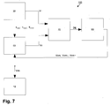
- the present invention has a calibration circuit 100, as described with reference to an embodiment in FIG Fig. 7 illustrates:
- the calibration circuit 100 according to Fig. 7 has two additional oscillators 30, 50 of substantially the same type as those described above with reference to FIG Fig. 4 described main oscillator 10 on.
- these two additional oscillators 30, 50 can be operated at a much lower frequency and thus with much lower power consumption than the main oscillator 10; however, these two additional oscillators 30, 50 have substantially the same tuning characteristics as the main oscillator 10.
- One of the two additional oscillators 30, 50 is a based Fig. 8
- the anodic terminal of a first varactor 52 of the calibration oscillator 50 is supplied with the first tuning voltage Vcm and the second tuning voltage Vcm-, and the anodic terminal of a second varactor 54 of the calibration oscillator 50 is supplied with the first tuning voltage Vcm and the third tuning voltage Vcm +.
- the cathodic terminal of the first varactor 52 and the cathodic terminal of the second varactor 54 are connected to one another, to the source contact or emitter terminal of a first transistor 62 of the calibration oscillator 50 and to the drain contact or collector terminal of a second transistor 64 of the calibration oscillator 50.
- the anodic terminal of a third varactor 56 of the calibration oscillator 50 is supplied with the first tuning voltage Vcm and the second tuning voltage Vcm-, and the anodic terminal of a fourth varactor 58 of the calibration oscillator 50 is supplied with the first tuning voltage Vcm and the third tuning voltage Vcm +.
- the cathodic terminal of the third varactor 56 and the cathodic terminal of the fourth varactor 58 are connected to each other, to the source contact or emitter terminal of a third transistor 66 of the calibration oscillator 50 and to the drain contact or collector terminal of a fourth transistor 68 of the calibration oscillator 50.
- the source contact or emitter terminal of the second transistor 64 and the source contact or emitter terminal of the fourth transistor 68 are connected to one another and to a current source 60 connected.
- the gate contact or base terminal of the first transistor 62 and the gate contact or base terminal of the third transistor 66 are connected to each other and are applied with a bias voltage or bias voltage Vbias.
- the drain contact or collector terminal of the first transistor 62 and the drain contact or collector terminal of the third transistor 66 provide the output signal Vc of the calibration oscillator 50.
- the other of the two additional oscillators 30, 50 is a based Fig. 9 Exemplary illustrated reference oscillator 30 which is associated with the calibration oscillator 50 in terms of timing.
- the anodic terminal of a first varactor 32 of the reference oscillator 30 and the anodic terminal of a second varactor 34 of the reference oscillator 30 are subjected to a reference potential or reference potential GND, namely ground potential or ground potential or zero potential.
- the cathodic terminal of the first varactor 32 and the cathodic terminal of the second varactor 34 are connected to one another, to the source contact or emitter terminal of a first transistor 42 of the reference oscillator 30 and to the drain contact or collector terminal of a second transistor 44 of the reference oscillator 30.
- the anodic terminal of a third varactor 36 of the reference oscillator 30 and the anodic terminal of a fourth varactor 38 of the reference oscillator 30 are supplied with the reference potential or reference potential GND, namely with ground potential or ground potential or zero potential.
- the cathodic terminal of the third varactor 36 and the cathodic terminal of the fourth varactor 38 are connected to one another, to the source contact or emitter terminal of a third transistor 46 of the reference oscillator 30 and to the drain contact or collector terminal of a fourth transistor 48 of the reference oscillator 30.
- the source contact or emitter terminal of the second transistor 44 and the source contact or emitter terminal of the fourth transistor 48 are connected to one another and to a current source 40.
- the gate contact or base terminal of the first transistor 42 and the gate contact or base terminal of the third transistor 46 are connected to each other and are applied with a bias voltage or bias voltage Vbias.
- the drain contact or collector terminal of the first transistor 42 and the drain contact or collector terminal of the third transistor 46 provide the output signal Vr of the reference oscillator 30.
- varactor diodes or tuning diodes or varicabs 12, 14, 32, 34, 36, 38, 52, 54, 56, 58 are electronic semiconductor devices in which a variation occurs by changing the applied voltage the capacity of for example 10 to 1 reach, so that an electrically controllable capacity is available.
- a portion of the aforementioned transistors 22, 24, 26, 28, 42, 44, 46, 48, 62, 64, 66, 68 may or all of the aforementioned transistors 22, 24, 26, 28, 42, 44, 46, 48, 62nd , 64, 66, 68 can be used, in particular, as field-effect transistors (FETs), for example as metal oxide semiconductor field-effect transistors (MOSFETs), such as n-type field effect transistors.
- MOSFETs metal oxide semiconductor field-effect transistors
- n-type MOSFETs may be formed.
- a clock counter 70 (so-called clock cycle error counter) connected downstream of the calibration oscillator 50 and the reference oscillator 30 compares the respective number N of clocks (clock cycles) of the calibration oscillator 50 on the basis of the output signal Vc of the calibration oscillator 50 and of the output signal Vr of the reference oscillator 30. of the reference oscillator 30 and forms the difference.
- N clock error DE (so-called clock cycle error) is integrated in the clock counter 70 and provided as a digital bus signal to the clock counter 70 subsequent digital-to-analog converter 90 as an input signal.
- the digital-to-analog converter 90 converts the clock error DE into an analog signal which sets the tuning voltage Vcm, Vcm-, Vcm + in the calibration oscillator 50 to the correct value.
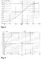
- Fig. 10 exemplifies the calculations of the calibration circuit 100, in particular accuracy, standard deviation ⁇ , necessary counter length of the clock counter 70, bit width of the digital-to-analog converter 90 and the like.
Landscapes
- Engineering & Computer Science (AREA)
- Computer Networks & Wireless Communication (AREA)
- Signal Processing (AREA)
- Inductance-Capacitance Distribution Constants And Capacitance-Resistance Oscillators (AREA)
- Stabilization Of Oscillater, Synchronisation, Frequency Synthesizers (AREA)
- Manipulation Of Pulses (AREA)
Applications Claiming Priority (2)
| Application Number | Priority Date | Filing Date | Title |
|---|---|---|---|
| DE102012104472 | 2012-05-23 | ||
| PCT/DE2013/200016 WO2013174377A2 (de) | 2012-05-23 | 2013-05-23 | Schaltungsanordnung und verfahren zum kalibrieren von ansteuersignalen für spannungsgesteuerte oszillatoren |
Publications (2)
| Publication Number | Publication Date |
|---|---|
| EP2853029A2 EP2853029A2 (de) | 2015-04-01 |
| EP2853029B1 true EP2853029B1 (de) | 2016-05-18 |
Family
ID=48537785
Family Applications (1)
| Application Number | Title | Priority Date | Filing Date |
|---|---|---|---|
| EP13756304.5A Active EP2853029B1 (de) | 2012-05-23 | 2013-05-23 | Schaltungsanordnung und verfahren zum kalibrieren von ansteuersignalen für spannungsgesteuerte oszillatoren |
Country Status (5)
| Country | Link |
|---|---|
| US (1) | US9484929B2 (https=) |
| EP (1) | EP2853029B1 (https=) |
| JP (1) | JP6460980B2 (https=) |
| DE (1) | DE112013002663A5 (https=) |
| WO (1) | WO2013174377A2 (https=) |
Cited By (1)
| Publication number | Priority date | Publication date | Assignee | Title |
|---|---|---|---|---|
| US12603655B1 (en) * | 2024-04-02 | 2026-04-14 | Cadence Design Systems, Inc. | Subranging digital to time converter-based fractional phase locked loop architecture |
Families Citing this family (3)
| Publication number | Priority date | Publication date | Assignee | Title |
|---|---|---|---|---|
| JP7215737B2 (ja) | 2016-07-14 | 2023-01-31 | シリコン・ライン・ゲー・エム・ベー・ハー | 電気信号を制御可能に遅延させるためのデバイス及び方法 |
| CN111404545B (zh) * | 2020-04-20 | 2022-07-29 | 成都华微电子科技股份有限公司 | 带数字修调功能的振荡器电路和时钟信号生成方法 |
| CN111934678B (zh) * | 2020-09-28 | 2021-01-05 | 深圳英集芯科技有限公司 | 芯片内时钟频率自动校准方法及相关产品 |
Family Cites Families (8)
| Publication number | Priority date | Publication date | Assignee | Title |
|---|---|---|---|---|
| US5726607A (en) * | 1992-06-15 | 1998-03-10 | Adc Telecommunications, Inc. | Phase locked loop using a counter and a microcontroller to produce VCXO control signals |
| US5631920A (en) * | 1993-11-29 | 1997-05-20 | Lexmark International, Inc. | Spread spectrum clock generator |
| US6259326B1 (en) * | 1999-08-24 | 2001-07-10 | Agere Systems Guardian Corp. | Clock recovery from a burst-mode digital signal each packet of which may have one of several predefined frequencies |
| JP4089938B2 (ja) * | 2000-06-09 | 2008-05-28 | 日本電信電話株式会社 | 電圧制御発振器 |
| US7129763B1 (en) * | 2004-11-08 | 2006-10-31 | Western Digital Technologies, Inc. | Adjusting power consumption of digital circuitry by generating frequency error representing error in propagation delay |
| JP4733152B2 (ja) * | 2008-01-31 | 2011-07-27 | 日本電信電話株式会社 | 周波数制御回路およびcdr回路 |
| JP2010178148A (ja) * | 2009-01-30 | 2010-08-12 | Hitachi Kokusai Electric Inc | バッファ回路 |
| US8125285B2 (en) * | 2009-09-10 | 2012-02-28 | Analog Devices, Inc. | Digitally controlled oscillators |
-
2013
- 2013-05-23 WO PCT/DE2013/200016 patent/WO2013174377A2/de not_active Ceased
- 2013-05-23 EP EP13756304.5A patent/EP2853029B1/de active Active
- 2013-05-23 DE DE112013002663.5T patent/DE112013002663A5/de not_active Withdrawn
- 2013-05-23 JP JP2015513018A patent/JP6460980B2/ja not_active Expired - Fee Related
-
2014
- 2014-11-24 US US14/552,173 patent/US9484929B2/en active Active
Cited By (1)
| Publication number | Priority date | Publication date | Assignee | Title |
|---|---|---|---|---|
| US12603655B1 (en) * | 2024-04-02 | 2026-04-14 | Cadence Design Systems, Inc. | Subranging digital to time converter-based fractional phase locked loop architecture |
Also Published As
| Publication number | Publication date |
|---|---|
| JP6460980B2 (ja) | 2019-01-30 |
| JP2015525499A (ja) | 2015-09-03 |
| WO2013174377A3 (de) | 2014-01-30 |
| US9484929B2 (en) | 2016-11-01 |
| WO2013174377A2 (de) | 2013-11-28 |
| EP2853029A2 (de) | 2015-04-01 |
| DE112013002663A5 (de) | 2015-06-18 |
| US20150381185A1 (en) | 2015-12-31 |
Similar Documents
| Publication | Publication Date | Title |
|---|---|---|
| DE10321200B3 (de) | Einrichtung und Verfahren zur Kalibrierung von R/C-Filterschaltungen | |
| DE69412306T2 (de) | Temperaturkompensierter Quarzoszillator | |
| EP3335012B1 (de) | Elektronische steuerungseinheit | |
| DE102006047958B4 (de) | Generator für eine exakte Dreieckssignalform | |
| DE102008023680B4 (de) | Spannungsgesteuerte Oszillatorschaltung | |
| EP2853029B1 (de) | Schaltungsanordnung und verfahren zum kalibrieren von ansteuersignalen für spannungsgesteuerte oszillatoren | |
| DE4139117C1 (https=) | ||
| DE102007009525A1 (de) | Konzept zum Erzeugen eines versorgungsspannungsabhängigen Taktsignals | |
| EP0974196B1 (de) | Digitale afc-einstellung durch reziproke dds | |
| DE102018216614A1 (de) | Kalibrieren eines injektionssynchronisierten oszillators | |
| DE102019201411B3 (de) | Synchronisation einer integrierten Schaltung mit Sensor | |
| DE3128331A1 (de) | "c-mos-oszillatorschaltung" | |
| DE2349749A1 (de) | Oszillator | |
| EP3653991A1 (de) | Verfahren zur automatischen frequenzanpassung eines filters in einer geschlossenen regelschleife | |
| EP1525662B1 (de) | Digital gesteuerter oszillator | |
| DE102013005055A1 (de) | Erzeugen einer abgestimmten Frequenzausgabe aus einem Signalgenerator | |
| DE102006032276B4 (de) | Amplitudenregelungsschaltung | |
| EP1588483B1 (de) | Vorrichtung und verfahren zur frequenzsynthese | |
| WO2013189494A2 (de) | Schaltungsanordnung und verfahren zur takt- und/oder datenrückgewinnung | |
| DE10260713B4 (de) | Digital steuerbarer Oszillator | |
| DE2310314C3 (de) | Regelschaltung zur Erzeugung eines Signals konstanter Frequenz für einen elektronischen Zeitgeber | |
| DE10319899B4 (de) | Verfahren und Frequenzvergleichseinrichtung zum Erzeugen eines Kontrollsignals, das eine Frequenzabweichung anzeigt | |
| DE3113800A1 (de) | Frequenzmodulator | |
| DE10049531C2 (de) | Taktgenerator | |
| DE3024014A1 (de) | Wechsel- in gleichspannungswandler in form einer integrierten schaltung |
Legal Events
| Date | Code | Title | Description |
|---|---|---|---|
| PUAI | Public reference made under article 153(3) epc to a published international application that has entered the european phase |
Free format text: ORIGINAL CODE: 0009012 |
|
| 17P | Request for examination filed |
Effective date: 20141223 |
|
| AK | Designated contracting states |
Kind code of ref document: A2 Designated state(s): AL AT BE BG CH CY CZ DE DK EE ES FI FR GB GR HR HU IE IS IT LI LT LU LV MC MK MT NL NO PL PT RO RS SE SI SK SM TR |
|
| AX | Request for extension of the european patent |
Extension state: BA ME |
|
| DAX | Request for extension of the european patent (deleted) | ||
| GRAP | Despatch of communication of intention to grant a patent |
Free format text: ORIGINAL CODE: EPIDOSNIGR1 |
|
| INTG | Intention to grant announced |
Effective date: 20151123 |
|
| GRAS | Grant fee paid |
Free format text: ORIGINAL CODE: EPIDOSNIGR3 |
|
| GRAA | (expected) grant |
Free format text: ORIGINAL CODE: 0009210 |
|
| RAP1 | Party data changed (applicant data changed or rights of an application transferred) |
Owner name: SILICON LINE GMBH |
|
| AK | Designated contracting states |
Kind code of ref document: B1 Designated state(s): AL AT BE BG CH CY CZ DE DK EE ES FI FR GB GR HR HU IE IS IT LI LT LU LV MC MK MT NL NO PL PT RO RS SE SI SK SM TR |
|
| REG | Reference to a national code |
Ref country code: GB Ref legal event code: FG4D Free format text: NOT ENGLISH |
|
| REG | Reference to a national code |
Ref country code: FR Ref legal event code: PLFP Year of fee payment: 4 |
|
| REG | Reference to a national code |
Ref country code: CH Ref legal event code: EP |
|
| REG | Reference to a national code |
Ref country code: IE Ref legal event code: FG4D Free format text: LANGUAGE OF EP DOCUMENT: GERMAN Ref country code: AT Ref legal event code: REF Ref document number: 801234 Country of ref document: AT Kind code of ref document: T Effective date: 20160615 |
|
| REG | Reference to a national code |
Ref country code: DE Ref legal event code: R096 Ref document number: 502013003086 Country of ref document: DE |
|
| REG | Reference to a national code |
Ref country code: NL Ref legal event code: MP Effective date: 20160518 |
|
| REG | Reference to a national code |
Ref country code: LT Ref legal event code: MG4D |
|
| PG25 | Lapsed in a contracting state [announced via postgrant information from national office to epo] |
Ref country code: NO Free format text: LAPSE BECAUSE OF FAILURE TO SUBMIT A TRANSLATION OF THE DESCRIPTION OR TO PAY THE FEE WITHIN THE PRESCRIBED TIME-LIMIT Effective date: 20160818 Ref country code: NL Free format text: LAPSE BECAUSE OF FAILURE TO SUBMIT A TRANSLATION OF THE DESCRIPTION OR TO PAY THE FEE WITHIN THE PRESCRIBED TIME-LIMIT Effective date: 20160518 Ref country code: FI Free format text: LAPSE BECAUSE OF FAILURE TO SUBMIT A TRANSLATION OF THE DESCRIPTION OR TO PAY THE FEE WITHIN THE PRESCRIBED TIME-LIMIT Effective date: 20160518 Ref country code: LT Free format text: LAPSE BECAUSE OF FAILURE TO SUBMIT A TRANSLATION OF THE DESCRIPTION OR TO PAY THE FEE WITHIN THE PRESCRIBED TIME-LIMIT Effective date: 20160518 |
|
| PG25 | Lapsed in a contracting state [announced via postgrant information from national office to epo] |
Ref country code: SE Free format text: LAPSE BECAUSE OF FAILURE TO SUBMIT A TRANSLATION OF THE DESCRIPTION OR TO PAY THE FEE WITHIN THE PRESCRIBED TIME-LIMIT Effective date: 20160518 Ref country code: HR Free format text: LAPSE BECAUSE OF FAILURE TO SUBMIT A TRANSLATION OF THE DESCRIPTION OR TO PAY THE FEE WITHIN THE PRESCRIBED TIME-LIMIT Effective date: 20160518 Ref country code: ES Free format text: LAPSE BECAUSE OF FAILURE TO SUBMIT A TRANSLATION OF THE DESCRIPTION OR TO PAY THE FEE WITHIN THE PRESCRIBED TIME-LIMIT Effective date: 20160518 Ref country code: LV Free format text: LAPSE BECAUSE OF FAILURE TO SUBMIT A TRANSLATION OF THE DESCRIPTION OR TO PAY THE FEE WITHIN THE PRESCRIBED TIME-LIMIT Effective date: 20160518 Ref country code: RS Free format text: LAPSE BECAUSE OF FAILURE TO SUBMIT A TRANSLATION OF THE DESCRIPTION OR TO PAY THE FEE WITHIN THE PRESCRIBED TIME-LIMIT Effective date: 20160518 Ref country code: GR Free format text: LAPSE BECAUSE OF FAILURE TO SUBMIT A TRANSLATION OF THE DESCRIPTION OR TO PAY THE FEE WITHIN THE PRESCRIBED TIME-LIMIT Effective date: 20160819 Ref country code: PT Free format text: LAPSE BECAUSE OF FAILURE TO SUBMIT A TRANSLATION OF THE DESCRIPTION OR TO PAY THE FEE WITHIN THE PRESCRIBED TIME-LIMIT Effective date: 20160919 |
|
| PG25 | Lapsed in a contracting state [announced via postgrant information from national office to epo] |
Ref country code: IT Free format text: LAPSE BECAUSE OF FAILURE TO SUBMIT A TRANSLATION OF THE DESCRIPTION OR TO PAY THE FEE WITHIN THE PRESCRIBED TIME-LIMIT Effective date: 20160518 |
|
| PG25 | Lapsed in a contracting state [announced via postgrant information from national office to epo] |
Ref country code: EE Free format text: LAPSE BECAUSE OF FAILURE TO SUBMIT A TRANSLATION OF THE DESCRIPTION OR TO PAY THE FEE WITHIN THE PRESCRIBED TIME-LIMIT Effective date: 20160518 Ref country code: RO Free format text: LAPSE BECAUSE OF FAILURE TO SUBMIT A TRANSLATION OF THE DESCRIPTION OR TO PAY THE FEE WITHIN THE PRESCRIBED TIME-LIMIT Effective date: 20160518 Ref country code: DK Free format text: LAPSE BECAUSE OF FAILURE TO SUBMIT A TRANSLATION OF THE DESCRIPTION OR TO PAY THE FEE WITHIN THE PRESCRIBED TIME-LIMIT Effective date: 20160518 Ref country code: SK Free format text: LAPSE BECAUSE OF FAILURE TO SUBMIT A TRANSLATION OF THE DESCRIPTION OR TO PAY THE FEE WITHIN THE PRESCRIBED TIME-LIMIT Effective date: 20160518 Ref country code: CZ Free format text: LAPSE BECAUSE OF FAILURE TO SUBMIT A TRANSLATION OF THE DESCRIPTION OR TO PAY THE FEE WITHIN THE PRESCRIBED TIME-LIMIT Effective date: 20160518 |
|
| REG | Reference to a national code |
Ref country code: DE Ref legal event code: R097 Ref document number: 502013003086 Country of ref document: DE |
|
| REG | Reference to a national code |
Ref country code: IE Ref legal event code: MM4A |
|
| PG25 | Lapsed in a contracting state [announced via postgrant information from national office to epo] |
Ref country code: SM Free format text: LAPSE BECAUSE OF FAILURE TO SUBMIT A TRANSLATION OF THE DESCRIPTION OR TO PAY THE FEE WITHIN THE PRESCRIBED TIME-LIMIT Effective date: 20160518 Ref country code: PL Free format text: LAPSE BECAUSE OF FAILURE TO SUBMIT A TRANSLATION OF THE DESCRIPTION OR TO PAY THE FEE WITHIN THE PRESCRIBED TIME-LIMIT Effective date: 20160518 |
|
| PLBE | No opposition filed within time limit |
Free format text: ORIGINAL CODE: 0009261 |
|
| STAA | Information on the status of an ep patent application or granted ep patent |
Free format text: STATUS: NO OPPOSITION FILED WITHIN TIME LIMIT |
|
| PG25 | Lapsed in a contracting state [announced via postgrant information from national office to epo] |
Ref country code: MC Free format text: LAPSE BECAUSE OF FAILURE TO SUBMIT A TRANSLATION OF THE DESCRIPTION OR TO PAY THE FEE WITHIN THE PRESCRIBED TIME-LIMIT Effective date: 20160518 |
|
| 26N | No opposition filed |
Effective date: 20170221 |
|
| REG | Reference to a national code |
Ref country code: FR Ref legal event code: PLFP Year of fee payment: 5 |
|
| PG25 | Lapsed in a contracting state [announced via postgrant information from national office to epo] |
Ref country code: SI Free format text: LAPSE BECAUSE OF FAILURE TO SUBMIT A TRANSLATION OF THE DESCRIPTION OR TO PAY THE FEE WITHIN THE PRESCRIBED TIME-LIMIT Effective date: 20160518 Ref country code: IE Free format text: LAPSE BECAUSE OF NON-PAYMENT OF DUE FEES Effective date: 20160523 |
|
| REG | Reference to a national code |
Ref country code: FR Ref legal event code: PLFP Year of fee payment: 6 |
|
| PG25 | Lapsed in a contracting state [announced via postgrant information from national office to epo] |
Ref country code: HU Free format text: LAPSE BECAUSE OF FAILURE TO SUBMIT A TRANSLATION OF THE DESCRIPTION OR TO PAY THE FEE WITHIN THE PRESCRIBED TIME-LIMIT; INVALID AB INITIO Effective date: 20130523 |
|
| PG25 | Lapsed in a contracting state [announced via postgrant information from national office to epo] |
Ref country code: CY Free format text: LAPSE BECAUSE OF FAILURE TO SUBMIT A TRANSLATION OF THE DESCRIPTION OR TO PAY THE FEE WITHIN THE PRESCRIBED TIME-LIMIT Effective date: 20160518 Ref country code: MT Free format text: LAPSE BECAUSE OF FAILURE TO SUBMIT A TRANSLATION OF THE DESCRIPTION OR TO PAY THE FEE WITHIN THE PRESCRIBED TIME-LIMIT Effective date: 20160518 Ref country code: LU Free format text: LAPSE BECAUSE OF NON-PAYMENT OF DUE FEES Effective date: 20160523 Ref country code: IS Free format text: LAPSE BECAUSE OF FAILURE TO SUBMIT A TRANSLATION OF THE DESCRIPTION OR TO PAY THE FEE WITHIN THE PRESCRIBED TIME-LIMIT Effective date: 20160518 Ref country code: MK Free format text: LAPSE BECAUSE OF FAILURE TO SUBMIT A TRANSLATION OF THE DESCRIPTION OR TO PAY THE FEE WITHIN THE PRESCRIBED TIME-LIMIT Effective date: 20160518 |
|
| PG25 | Lapsed in a contracting state [announced via postgrant information from national office to epo] |
Ref country code: BG Free format text: LAPSE BECAUSE OF FAILURE TO SUBMIT A TRANSLATION OF THE DESCRIPTION OR TO PAY THE FEE WITHIN THE PRESCRIBED TIME-LIMIT Effective date: 20160518 |
|
| PG25 | Lapsed in a contracting state [announced via postgrant information from national office to epo] |
Ref country code: AL Free format text: LAPSE BECAUSE OF FAILURE TO SUBMIT A TRANSLATION OF THE DESCRIPTION OR TO PAY THE FEE WITHIN THE PRESCRIBED TIME-LIMIT Effective date: 20160518 Ref country code: TR Free format text: LAPSE BECAUSE OF FAILURE TO SUBMIT A TRANSLATION OF THE DESCRIPTION OR TO PAY THE FEE WITHIN THE PRESCRIBED TIME-LIMIT Effective date: 20160518 |
|
| REG | Reference to a national code |
Ref country code: AT Ref legal event code: MM01 Ref document number: 801234 Country of ref document: AT Kind code of ref document: T Effective date: 20180523 |
|
| PG25 | Lapsed in a contracting state [announced via postgrant information from national office to epo] |
Ref country code: AT Free format text: LAPSE BECAUSE OF NON-PAYMENT OF DUE FEES Effective date: 20180523 |
|
| PGFP | Annual fee paid to national office [announced via postgrant information from national office to epo] |
Ref country code: CH Payment date: 20210830 Year of fee payment: 9 |
|
| REG | Reference to a national code |
Ref country code: CH Ref legal event code: PL |
|
| PG25 | Lapsed in a contracting state [announced via postgrant information from national office to epo] |
Ref country code: LI Free format text: LAPSE BECAUSE OF NON-PAYMENT OF DUE FEES Effective date: 20220531 Ref country code: CH Free format text: LAPSE BECAUSE OF NON-PAYMENT OF DUE FEES Effective date: 20220531 |
|
| P01 | Opt-out of the competence of the unified patent court (upc) registered |
Effective date: 20230527 |
|
| PGFP | Annual fee paid to national office [announced via postgrant information from national office to epo] |
Ref country code: BE Payment date: 20230530 Year of fee payment: 11 |
|
| PGFP | Annual fee paid to national office [announced via postgrant information from national office to epo] |
Ref country code: GB Payment date: 20230630 Year of fee payment: 11 |
|
| GBPC | Gb: european patent ceased through non-payment of renewal fee |
Effective date: 20240523 |
|
| REG | Reference to a national code |
Ref country code: BE Ref legal event code: MM Effective date: 20240531 |
|
| PG25 | Lapsed in a contracting state [announced via postgrant information from national office to epo] |
Ref country code: BE Free format text: LAPSE BECAUSE OF NON-PAYMENT OF DUE FEES Effective date: 20240531 |
|
| PG25 | Lapsed in a contracting state [announced via postgrant information from national office to epo] |
Ref country code: GB Free format text: LAPSE BECAUSE OF NON-PAYMENT OF DUE FEES Effective date: 20240523 |
|
| PGFP | Annual fee paid to national office [announced via postgrant information from national office to epo] |
Ref country code: FR Payment date: 20250602 Year of fee payment: 13 |
|
| PGFP | Annual fee paid to national office [announced via postgrant information from national office to epo] |
Ref country code: DE Payment date: 20250731 Year of fee payment: 13 |