EP2840608A2 - Vorspannungsunempfindlicher BIGFET-ESD-Versorungsschutz - Google Patents
Vorspannungsunempfindlicher BIGFET-ESD-Versorungsschutz Download PDFInfo
- Publication number
- EP2840608A2 EP2840608A2 EP20140173944 EP14173944A EP2840608A2 EP 2840608 A2 EP2840608 A2 EP 2840608A2 EP 20140173944 EP20140173944 EP 20140173944 EP 14173944 A EP14173944 A EP 14173944A EP 2840608 A2 EP2840608 A2 EP 2840608A2
- Authority
- EP
- European Patent Office
- Prior art keywords
- bigfet
- esd
- node
- protection device
- voltage
- Prior art date
- Legal status (The legal status is an assumption and is not a legal conclusion. Google has not performed a legal analysis and makes no representation as to the accuracy of the status listed.)
- Granted
Links
Images




Classifications
-
- H—ELECTRICITY
- H02—GENERATION; CONVERSION OR DISTRIBUTION OF ELECTRIC POWER
- H02H—EMERGENCY PROTECTIVE CIRCUIT ARRANGEMENTS
- H02H9/00—Emergency protective circuit arrangements for limiting excess current or voltage without disconnection
- H02H9/04—Emergency protective circuit arrangements for limiting excess current or voltage without disconnection responsive to excess voltage
- H02H9/045—Emergency protective circuit arrangements for limiting excess current or voltage without disconnection responsive to excess voltage adapted to a particular application and not provided for elsewhere
- H02H9/046—Emergency protective circuit arrangements for limiting excess current or voltage without disconnection responsive to excess voltage adapted to a particular application and not provided for elsewhere responsive to excess voltage appearing at terminals of integrated circuits
-
- H—ELECTRICITY
- H03—ELECTRONIC CIRCUITRY
- H03K—PULSE TECHNIQUE
- H03K19/00—Logic circuits, i.e. having at least two inputs acting on one output; Inverting circuits
- H03K19/003—Modifications for increasing the reliability for protection
- H03K19/00315—Modifications for increasing the reliability for protection in field-effect transistor circuits
-
- H—ELECTRICITY
- H10—SEMICONDUCTOR DEVICES; ELECTRIC SOLID-STATE DEVICES NOT OTHERWISE PROVIDED FOR
- H10D—INORGANIC ELECTRIC SEMICONDUCTOR DEVICES
- H10D89/00—Aspects of integrated devices not covered by groups H10D84/00 - H10D88/00
- H10D89/60—Integrated devices comprising arrangements for electrical or thermal protection, e.g. protection circuits against electrostatic discharge [ESD]
- H10D89/601—Integrated devices comprising arrangements for electrical or thermal protection, e.g. protection circuits against electrostatic discharge [ESD] for devices having insulated gate electrodes, e.g. for IGFETs or IGBTs
- H10D89/811—Integrated devices comprising arrangements for electrical or thermal protection, e.g. protection circuits against electrostatic discharge [ESD] for devices having insulated gate electrodes, e.g. for IGFETs or IGBTs using FETs as protective elements
- H10D89/819—Bias arrangements for gate electrodes of FETs, e.g. RC networks or voltage partitioning circuits
Definitions
- Embodiments of the invention relate generally to electronic hardware and methods for operating electronic hardware, and, more particularly, to electrostatic discharge (ESD) protection devices and methods for providing ESD protection for an integrated circuit (IC) device.
- ESD electrostatic discharge
- An ESD protection circuit can be integrated onto an IC chip to provide a low impedance channel to ground to prevent thermal damage in the IC substrate.
- a common ESD protection circuit which is known as "railclamp," includes a bigFET and a trigger circuit for activating the bigFET during an ESD strike.
- a bigFET is an n-channel MOSFET (NMOS) transistor with a large channel width.
- NMOS n-channel MOSFET
- PMOS p-channel MOSFET
- a bigFET based ESD protection device can be used to protect a supply domain of an IC chip from overheating during an ESD strike by shunting the ESD current from the supply domain to the ground domain.
- ESD test such as a human-body-model (HBM) test, a machine-model (MM) test, or a charged-device-model (CDM) test
- HBM human-body-model
- MM machine-model
- CDM charged-device-model
- a special class of ESD pulse is the so-called "system-level ESD pulse," as described in the International Electrotechnical Commission (IEC) -61000-4-2 standard.
- IEC International Electrotechnical Commission
- MM or CDM pulses these system level ESD pulses can be delivered to an IC chip when the IC chip is powered or unpowered.
- a conventional trigger circuit for a bigFET is typically designed without considering the possibility that the trigger circuit may be biased to some voltage level while an ESD pulse is delivered.
- a bigFET based ESD protection device may also be used as on-chip ESD protection for an IC chip against an ESD pulse, which is delivered while the IC chip is powered as well as unpowered.
- a railclamp with a conventional trigger circuit is used to protect an IC chip against system level ESD pulses, the performance of that railclamp can deteriorate when a system level ESD pulse is applied to the IC chip while the IC chip is in a powered state. Therefore, there is a need for a trigger device for a bigFET based ESD protection device that works with or without the presence of a pre-bias that is up to the maximum allowed supply voltage of an IC chip.
- an ESD protection device for an IC device includes a bigFET configured to conduct an ESD current during an ESD event and a trigger device configured to trigger the bigFET during the ESD event.
- the trigger device includes a slew rate detector configured to detect the ESD event, a driver stage configured to drive the bigFET, and a keep-on latch configured to keep the driver stage turned on to drive a gate terminal of the bigFET with a driving voltage that is insensitive to a pre-bias on a drain terminal or a source terminal of the bigFET.
- the trigger circuit can drive the bigFET with a driving voltage that is insensitive to a pre-bias on the bigFET, the performance of the trigger circuit is insensitive to the pre-bias on the bigFET. Consequently, the ESD protection circuit can be used as on-chip ESD protection for the IC device against an ESD pulse, regardless of whether the IC device is powered or unpowered. Other embodiments are also described.
- an ESD protection device for an IC device includes a bigFET configured to conduct an ESD current during an ESD event and a trigger device configured to trigger the bigFET during the ESD event.
- the trigger device includes a slew rate detector configured to detect the ESD event, a driver stage configured to drive the bigFET, and a keep-on latch configured to keep the driver stage turned on to drive a gate terminal of the bigFET with a driving voltage that is insensitive to a pre-bias on a drain terminal or the source terminal of the bigFET.
- an ESD protection device for an IC device includes a bigFET configured to conduct an ESD current during an ESD event and a trigger device configured to trigger the bigFET during the ESD event.
- a drain terminal or a source terminal of the bigFET is connected to a supply node to which the power supply voltage of the IC device is applied.
- the source terminal or the drain terminal of the bigFET is connected to a ground node to which the ground voltage is applied.
- the trigger device includes a slew rate detector configured to detect the ESD event, a driver stage configured to drive a gate terminal of the bigFET, a pre-driver stage configured to turn on the driver stage once the ESD event is detected by the slew rate detector, and a keep-on latch configured to keep the driver stage turned on for a time duration.
- the slew-rate detector includes a first capacitor and a first resistor.
- the driver stage includes a first transistor and a second resistor.
- the pre-driver stage includes a second transistor and a third resistor.
- the keep-on latch includes a third transistor, a second capacitor, and a fourth resistor.
- a method of providing ESD protection for an IC device involves triggering a bigFET during an ESD event of the IC device and conducting an ESD current using the bigFET during the ESD event.
- Triggering the bigFET involves detecting the ESD event, driving a gate terminal of the bigFET using a driver stage, and keeping the driver stage turned on to drive the gate terminal of the bigFET with a driving voltage that is insensitive to a pre-bias on a drain terminal or a source terminal of the bigFET.
- Fig. 1 is a schematic block diagram of an IC device 100 in accordance with an embodiment of the invention.
- the IC device includes a core circuit 102 and an ESD protection device 104 that is used to protect the core circuit during an ESD event, which may be an ESD test or an actual ESD strike.
- the IC device can be used in various applications, such as automotive applications, communications applications, industrial applications, medical applications, computer applications, and/or consumer or appliance applications.
- the IC device can be implemented in a substrate, such as a semiconductor wafer or a printed circuit board (PCB).
- the IC device is packaged as a semiconductor IC chip.
- the IC device may be included in a microcontroller, which can be used for, for example, in vehicle control or communications, identification, wireless communications, and/or lighting control.
- the IC device is included in a computing device, such as a smartphone, a tablet computer, a laptop, etc.
- the IC device may be included in a Near Field Communications (NFC) capable computing device.
- NFC Near Field Communications
- the core circuit 102 is a device to be protected by the ESD protection circuit in case of an ESD event.
- the core circuit typically includes one or more internal circuit components that are susceptible to ESD strikes. Examples of the core circuit include, but are not limited to, microcontrollers, transceivers, and switching circuits.
- the core circuit includes a power supply domain of the IC device 100.
- the core circuit may be connected to the power supply rail, "V DD ,” of the IC device 100.
- the IC device is shown in Fig. 1 as including the core circuit and the ESD protection device 104, in other embodiments, the IC device may include additional circuit elements.
- the IC device may include serially connected diodes that are coupled in parallel with the core circuit for current restriction and voltage surge protection.
- the ESD protection device 104 protects the core circuit 102 during an ESD event.
- the ESD protection device 104 can be used to protect a power supply domain of the IC device 100.
- the ESD protection device 104 may be connected to the power supply rail, "V DD ,” of the IC device 100.
- the ESD protection circuit 104 includes an ESD element 106 configured to conduct current during an ESD event and a trigger device 108 configured to trigger the ESD element during the ESD event.
- the ESD element 106 of the ESD protection device 104 can be implemented by any suitable semiconductor device.
- the ESD element is implemented as a bigFET, which is an NMOS with a large channel width or a PMOS transistor with a large channel width to sink ESD current.
- a bigFET can be used to protect a power supply domain of the IC device 100 from overvoltage during an ESD event by shunting the ESD current from the power supply domain to the ground domain (i.e., the ground).
- the channel width of a bigFET can be chosen to ensure that the voltage drop across the bigFET during an ESD event does not exceed a predetermined voltage, which is considered harmful to the inner circuit components (e.g., the core circuit 102) of the IC device.
- the predetermined voltage is typically set to be equal to or around (e.g., ⁇ 30%) the power supply voltage of the IC device.
- the trigger device 108 of the ESD protection device 104 is capable of detecting an ESD event and driving the ESD element 106 for a certain amount of time during an ESD event.
- the trigger device can be implemented using one or more capacitors, transistors, and/or resistors.
- the trigger device 108 includes a slew rate detector 110, an optional pre-driver stage 112, a keep-on latch 114, and a driver stage 116.
- the slew rate detector 110 is a circuit that is configured to detect an ESD event, which may be an ESD test or an actual ESD strike.
- the slew rate detector detects a rise in the power supply voltage, "V DD ,” of the IC device 100, which is characteristic of an ESD event.
- the pre-driver stage 112 is a circuit that is configured to turn on the driver stage 116 once an ESD event is detected by the slew rate detector.
- the pre-driver stage may be only active during the initial detection of an ESD event to "trigger" the driver stage.
- the trigger device does not include the pre-driver stage.
- the keep-on latch 114 is a circuit that is configured to keep the driver stage turned on for the expected maximum duration of the detected ESD event.
- the functions of the slew rate detector and the keep-on latch are implemented in a single circuit.
- the driver stage 116 is a circuit that is configured to drive the ESD element. In an embodiment in which the ESD element is implemented as a bigFET, the driver stage drives the gate terminal of the bigFET.
- Fig. 2 illustrates an example of the voltage bias and the ESD current path of the IC device 100 during an ESD event.
- dashed lines signify elements on a printed circuit board (PCB) while solid lines signify elements on an IC chip.
- the ESD event may be an ESD test on one of the input/output (I/O) pins of the IC device or an actual ESD strike.
- serially connected diodes 224, 226 and 228, 230 are connected in parallel with the core circuit 102 for current restriction and voltage surge protection purpose.
- the supply voltage, "V DD ,” from a power supply 222 is applied to the ESD protection device 104, causing the ESD protection device to be biased to some voltage between 0V and the power supply voltage, "V DD .”
- the power supply voltage, "V DD ” is not applied to the ESD protection device.
- electrical current flows through the serially connected diodes into the ESD protection device, as shown in arrows 232, 234, and flows into the ground (GND) through the ESD protection device, as shown in arrow 236.
- the keep-on latch 114 keeps the driver stage 116 on to drive the ESD element 106 with a voltage that is insensitive to the pre-bias on the ESD element.
- the trigger circuit 108 can drive the ESD element with a driving voltage that is independent from the power supply voltage, "V DD ,” of the IC device 100. Consequently, the performance of the trigger circuit 108 is insensitive to the voltage of the power supply voltage, "V DD ,” of the IC device.
- the trigger circuit 108 depicted in Fig. 1 allows the ESD protection circuit 104 to be used as on-chip ESD protection against an ESD pulse, which is delivered while the IC device is powered or unpowered.
- the trigger circuit 108 allows the ESD protection circuit 104 to be used in an International Electrotechnical Commission (IEC) 61000-4-2 Electrostatic Discharge Immunity Test, which can be delivered while the IC device 100 is in a powered state as well as in an unpowered state.
- the ESD protection circuit 104 can be either used as an extra clamp that sinks any residual current that other protection elements (e.g., on-board protection elements) fail to sink, or, to sink the entire system level ESD current of the IC device.
- the keep-on latch 114 may include a capacitor 118 that is configured to be charged by an ESD pulse of an ESD event and to keep the driver stage 116 on over the time interval that it takes for the capacitor to discharge, which is set to be longer than the time duration of a typical ESD pulse.
- the capacitor of the keep-on latch may not be directly connected to the power supply line, "V DD ,” of the IC device. Consequently, the presence of a positive voltage on the power supply line, "V DD ,” leaves the capacitor 118 of the keep-on latch 114 unbiased.
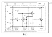
- Figs. 3-5 depict three embodiments of the ESD protection device 104 depicted in Fig. 1 that can be used as on-chip ESD protection against an ESD pulse, regardless of whether the IC device 100 is powered or unpowered.
- an ESD protection circuit 304, 404, or 504 includes a bigFET 306, 406, or 506 configured to conduct current during an ESD event and a trigger device 308, 408, or 508 configured to trigger/activate the bigFET during the ESD event.
- the ESD protection circuits 304, 304, 504 are some possible implementations of the ESD protection circuit 104 depicted in Fig. 1 . However, the ESD protection circuit 104 depicted in Fig.
- ESD protection circuits 304, 404, 504 depicted in Figs. 3-5 can be implemented differently from the ESD protection circuits 304, 404, 504 depicted in Figs. 3-5 .
- the invention is not restricted to the particular implementation of the ESD protection circuits 304, 404, 504 depicted in Figs. 3-5 .
- the ESD protection device 304 is based on the bigFET 306 that is implemented as an NMOS transistor, "M4."
- the trigger device 308 and the bigFET 306 are connected to a supply voltage, "V DD ,” at a power supply V DD node (e.g., a terminal or an input pad) 356 and a lower voltage, "V SS ,” at a voltage V SS node 358, which is set to a voltage that is zero (the ground) or around zero.
- the drain terminal, "D,” of the bigFET is connected to the V DD node 356, the source terminal, “S,” of the bigFET is connected to the V SS node 358, and the gate terminal, "G,” of the bigFET is connected to and controlled by the trigger circuit 308.
- the trigger circuit 308 biases the gate terminal, "G,” of the bigFET at the start of an ESD event such that the bigFET shunts the ESD current from the V DD node 356 to the V SS node 358 during the ESD event. By shunting the ESD current during the ESD event, the bigFET prevents ESD damage to itself and to all of the other circuits connected between the V DD node and the V SS node.
- the channel width of the bigFET is chosen such that the entire ESD current caused by the ESD event flows through the bigFET while keeping the voltage drop generated across the bigFET below a pre-determined critical value, which is typically set to a value between 50 % and 150 % of the nominal value of V DD .
- the trigger circuit 308 lifts the gate terminal, "G,” of the bigFET 306 to a positive voltage during an ESD event, keeps the gate terminal, "G,” of the bigFET at the same voltage as the V SS node 358 when there is no ESD event, and discriminates between an ESD event and a non-ESD event by detecting a change in the potential at the drain terminal, "D," of the bigFET.
- the trigger circuit sets the voltage on the gate terminal, "G,” of the bigFET to be equal to the voltage on the drain terminal, "D,” of the bigFET.
- the trigger circuit allows the voltage on the gate terminal, "G,” of the bigFET to assume the voltage of the source terminal, "S,” of the bigFET at all the times that no ESD event is occurring, so as to ensure a small stand-by leakage current of the bigFET.
- the trigger device 308 includes a slew rate detector 310, a pre-driver stage 312, a keep-on latch 314, and a driver stage 316.
- the slew-rate detector 310 includes a capacitor, "C1,” which is connected to the V DD node 356, and a resistor, "R1,” which is connected to the V SS node 358.
- the pre-driver stage 312 includes a resistor, "R3,” which is connected to the V DD node 356, and an NMOS transistor, "M1.”
- the gate terminal, “G,” of the NMOS transistor, “M1,” is connected to the capacitor, “C1,” and to the resistor, “R1,” the source terminal, “S,” of the NMOS transistor, “M1,” is connected to the V SS node 358, and the drain terminal, “D,” of the NMOS transistor, “M1,” is connected to the resistor, "R3.”
- the keep-on latch 314 includes a capacitor, “C2,” a resistor, "R2,” and an NMOS transistor, “M2.”
- the gate terminal, “G,” of the NMOS transistor, “M2” is connected to the capacitor, “C2,” and to the resistor, “R2,” the source terminal, “S,” of the NMOS transistor, “M2,” is connected to the V SS node 358, and the drain terminal,
- the driver stage 316 includes a PMOS transistor, "M3,” and a resistor, "R4.”
- the gate terminal, “G,” of the PMOS transistor, “M3,” is connected to the drain terminals of the NMOS transistors, “M1,” M2,” and to the resistor, "R3," the source terminal, “S,” of the PMOS transistor, “M3,” is connected to the V DD node 356, and the drain terminal, "D,” of the PMOS transistor, “M3,” is connected to the capacitor, "C2,” the resistor, "R4,” and to the gate terminal, "G,” of the bigFET 306.
- the resistor, “R4,” is connected to the V SS node 358 and to the gate terminal, "G,” of the bigFET 306.
- one or more capacitors of the trigger circuit 308 are replaced by one or more transistors.
- an NMOS transistor is used to replace a capacitor that is located between the voltage, "V SS ,” and some other node of the trigger circuit 308.
- a PMOS transistor can be used to replace a capacitor that is located between the voltage, "V DD " and some other node of the trigger circuit 308, or between two nodes of the trigger circuit 308 that are neither the V SS node 358 nor the V DD node 356.
- one or more resistors of the trigger circuit are replaced by one or more transistors, poly tracks, or implanted wells. The electrical connections between the circuit elements of the ESD protection device 304 may be direct or indirect through intermediate devices.
- a conventional trigger circuit capacitors are typically directly connected to a power supply node of an IC device. Consequently, the presence of a voltage on a power supply node of the IC device leaves capacitors of a conventional trigger circuit biased, causing a voltage difference at the drain and gate terminal of a bigFET, which renders the conventional trigger circuit less efficient.
- a pre-charge on the drain node of a bigFET also is present on a capacitor in the keep-on latch. Consequently, the drive voltage of the bigFET deteriorates when a pre-bias is present, which degrades the performance of the ESD protection.
- the capacitor, "C2,” of the keep-on latch 314 is connected to the drain terminal, "D" of the PMOS transistor, “M3,” of the driver stage 316.
- the capacitor, "C2,” of the keep-on latch 314 is connected to the gate terminal, "G,” of the bigFET 306 rather than to the drain terminal, "D,” of the bigFET.
- the voltage rise as a result of an ESD strike on the drain terminal, "D,” of the bigFET and the voltage rise on the gate terminal, "G,” of the bigFET, are nearly equal.
- the driving strength of the trigger circuit 308 is insensitive to a pre-bias on the power supply node 356 and the drain terminal, "D," of the bigFET 306 and the bigFET can function optimally at any reasonable pre-bias at the power supply node 356.
- the ESD protection circuit 304 can operate in the same fashion with or without pre-bias from the power supply of the IC device 100. Consequently, the ESD protection circuit 304 can be used in an IEC 61000-4-2 Electrostatic Discharge Immunity Test, which can be done when the IC device 100 is powered or unpowered.
- the ESD protection circuit 304 can be used as on-chip ESD protection for the IC device 100 against an ESD pulse, regardless of whether the IC device is powered or unpowered.
- an NMOS transistor is used as the bigFET 306.
- the invention is applicable to both an NMOS-based bigFET and a PMOS-based bigFET.
- Figs. 4 and 5 depict two embodiments of the ESD protection device 104 depicted in Fig. 1 that use a PMOS-based bigFET 406 or 506 to conduct current during an ESD event.
- an ESD protection circuit 404 includes the PMOS-based bigFET 406 configured to conduct current during an ESD event and a trigger device 408 configured to trigger/activate the bigFET 406 during the ESD event.
- the bigFET 406 is implemented as a PMOS transistor, "P3.”
- the trigger device 408 and the bigFET 406 are connected to a supply voltage, "V DD ,” at a power supply V DD node (e.g., a terminal or an input pad) 456 and a lower voltage, "V SS ,” at a voltage V SS node 458, which is set to a voltage that is zero (the ground) or around zero.
- the source terminal, "S,” of the bigFET 406 is connected to the V DD node 456, the drain terminal, "D,” of the bigFET 406 is connected to the V SS node 458, and the gate terminal, "G,” of the bigFET 406 is connected to and controlled by the trigger circuit 408.
- the trigger circuit 408 biases the gate terminal, "G," of the bigFET 406 at the start of an ESD event such that the bigFET 406 shunts the ESD current from the V DD node 456 to the V SS node 458 during the ESD event.
- the bigFET 406 prevents ESD damage to itself and to all of the other circuits connected between the V DD node 456 and the V SS node 458.
- the channel width of the bigFET 406 is chosen such that the entire ESD current caused by the ESD event flows through the bigFET 406 while keeping the voltage drop generated across the bigFET 406 below a pre-determined critical value, which is typically set to a value between 50 % and 150 % of the nominal value of V DD .
- the trigger device 408 includes a slew rate detector 410, a pre-driver stage 412, a keep-on latch 414, and a driver stage 416.
- the slew-rate detector 410 includes a capacitor, "C41,” which is connected to the V SS node 458, and a resistor, "R41,” which is connected to the V DD node 456.
- the pre-driver stage 412 includes a resistor, "R43,” which is connected to the V SS node 458, and a PMOS transistor, "P1.”
- the gate terminal, “G,” of the PMOS transistor, “P1,” is connected to the capacitor, "C41,” and to the resistor, "R41,” the source terminal, “S,” of the PMOS transistor, “P1,” is connected to the V DD node 456, and the drain terminal, "D,” of the PMOS transistor, “P1,” is connected to the resistor, "R43.”
- the keep-on latch 414 includes a capacitor, "C42,” a resistor, "R42,” and a PMOS transistor, "P2.”
- the gate terminal, “G,” of the PMOS transistor, “P2” is connected to the capacitor, "C42,” and to the resistor, “R42,” the source terminal, “S,” of the PMOS transistor, “P2,” is connected to the V DD node 456, and the drain terminal, “D,” of the PMOS
- the driver stage 416 includes an NMOS transistor, "N1,” and a resistor, "R44.”
- the gate terminal, "G,” of the NMOS transistor, “N1,” is connected to the drain terminals of the PMOS transistors, “P1,” P2,” and to the resistor, "R43,” the source terminal, “S,” of the NMOS transistor, “N1,” is connected to the V SS node 458, and the drain terminal, "D,” of the NMOS transistor, "N1,” is connected to the capacitor, "C42,” the resistor, "R44,” and to the gate terminal, "G,” of the bigFET 406.
- the resistor, “R44,” is connected to the V DD node 456 and to the gate terminal, "G,” of the bigFET 406.
- an ESD protection circuit 504 includes the PMOS-based bigFET 506 configured to conduct current during an ESD event and a trigger device 508 configured to trigger/activate the bigFET 506 during the ESD event.
- the bigFET 506 is implemented as a PMOS transistor, "P6.”
- the trigger device 508 and the bigFET 506 are connected to a supply voltage, "V DD ,” at a power supply V DD node (e.g., a terminal or an input pad) 556 and a lower voltage, "V SS ,” at a voltage V SS node 558, which is set to a voltage that is zero (the ground) or around zero.
- the source terminal, "S,” of the bigFET 506 is connected to the V DD node 556, the drain terminal, “D,” of the bigFET 506 is connected to the V SS node 558, and the gate terminal, "G,” of the bigFET 506 is connected to and controlled by the trigger circuit 508.
- the trigger circuit 508 biases the gate terminal, "G,” of the bigFET 506 at the start of an ESD event such that the bigFET 506 shunts the ESD current from the V DD node 556 to the V SS node 558 during the ESD event.
- the bigFET 506 prevents ESD damage to itself and to all of the other circuits connected between the V DD node 556 and the V SS node 558.
- the channel width of the bigFET 506 is chosen such that the entire ESD current caused by the ESD event flows through the bigFET 506 while keeping the voltage drop generated across the bigFET 506 below a pre-determined critical value, which is typically set to a value between 50 % and 150 % of the nominal value of V DD .
- the trigger device 508 includes a slew rate detector 510, a pre-driver stage 512, a keep-on latch 514, and a driver stage 516.
- the slew-rate detector 510 includes a capacitor, "C51,” which is connected to the V DD node 556, and a resistor, "R51,” which is connected to the V SS node 558.
- the pre-driver stage 512 includes a resistor, "R53,” which is connected to the V DD node 556, and an NMOS transistor, "N51.”
- the gate terminal, “G,” of the NMOS transistor, “N51,” is connected to the capacitor, "C51,” and to the resistor, "R51,” the source terminal, “S,” of the NMOS transistor, “N51,” is connected to the V SS node 558, and the drain terminal, “D,” of the NMOS transistor, “N51,” is connected to the resistor, "R53.”
- the keep-on latch 514 includes a capacitor, "C52,” a resistor, "R2,” and an NMOS transistor, “N52.” The gate terminal, “G,” of the NMOS transistor, “N52
- the driver stage 516 includes PMOS transistors, "P4,” “P5,” an NMOS transistor, “N53,” and a resistor, "R54.”
- the gate terminal, “G,” of the PMOS transistor, “P4,” is connected to the drain terminals of the NMOS transistors, "N51,” N52,” and to the resistor, "R53," the source terminal, “S,” of the PMOS transistor, “P4,” is connected to the V DD node 556, and the drain terminal, “D,” of the PMOS transistor, “P4,” is connected to the capacitor, "C2,” the resistor, "R54,” and to the gate terminals, “G,” of the transistors, “P5,” “N53.”
- the resistor, “R54,” is connected to the V SS node 558, to the gate terminals, “G,” of the transistors, “P5,” “N53,” and to the drain terminal, “D,” of the PMOS transistor, “P4.”
- Fig. 6 is a process flow diagram that illustrates a method for providing ESD protection for an IC device in accordance with an embodiment of the invention.
- the IC device may be the same as or similar to the IC device 100 depicted in Fig. 1 .
- a bigFET is triggered during an ESD event of the IC device by detecting the ESD event, driving a gate terminal of the bigFET using a driver stage, and keeping the driver stage turned on to drive the gate terminal of the bigFET with a driving voltage that is insensitive to a pre-bias on a drain terminal or a source terminal of the bigFET.
- an ESD current is conducted using the bigFET during the ESD event.
- the bigFET may be the same as or similar to the bigFETs 306, 406, 506 depicted in Figs. 3-5 .
Landscapes
- Engineering & Computer Science (AREA)
- Physics & Mathematics (AREA)
- Computer Hardware Design (AREA)
- Computing Systems (AREA)
- General Engineering & Computer Science (AREA)
- Mathematical Physics (AREA)
- Microelectronics & Electronic Packaging (AREA)
- Semiconductor Integrated Circuits (AREA)
- Metal-Oxide And Bipolar Metal-Oxide Semiconductor Integrated Circuits (AREA)
Applications Claiming Priority (1)
| Application Number | Priority Date | Filing Date | Title |
|---|---|---|---|
| US13/968,337 US9153958B2 (en) | 2013-08-15 | 2013-08-15 | Bias-insensitive trigger circuit for bigFET ESD supply protection |
Publications (3)
| Publication Number | Publication Date |
|---|---|
| EP2840608A2 true EP2840608A2 (de) | 2015-02-25 |
| EP2840608A3 EP2840608A3 (de) | 2015-08-05 |
| EP2840608B1 EP2840608B1 (de) | 2017-08-30 |
Family
ID=50980242
Family Applications (1)
| Application Number | Title | Priority Date | Filing Date |
|---|---|---|---|
| EP14173944.1A Active EP2840608B1 (de) | 2013-08-15 | 2014-06-25 | Vorspannungsunempfindlicher BIGFET-ESD-Versorungsschutz |
Country Status (3)
| Country | Link |
|---|---|
| US (1) | US9153958B2 (de) |
| EP (1) | EP2840608B1 (de) |
| CN (1) | CN104377670B (de) |
Families Citing this family (10)
| Publication number | Priority date | Publication date | Assignee | Title |
|---|---|---|---|---|
| CN107123977B (zh) * | 2016-02-24 | 2019-04-19 | 比亚迪股份有限公司 | 晶体管的驱动电路 |
| CN106356823B (zh) * | 2016-09-18 | 2018-08-14 | 无锡力芯微电子股份有限公司 | 集成于芯片内的浪涌保护电路 |
| DE102016218074B3 (de) * | 2016-09-21 | 2018-01-25 | Ifm Electronic Gmbh | Ratiometrisch arbeitendes Messgerät für die Prozessmesstechnik mit einer Überspannungsschutzeinheit |
| US10367349B2 (en) | 2017-03-31 | 2019-07-30 | Nxp B.V. | Electrostatic discharge (ESD) protection device and method for operating an ESD protection device |
| US11387649B2 (en) * | 2019-09-11 | 2022-07-12 | Vanguard International Semiconductor Corporation | Operating circuit having ESD protection function |
| CN111697533B (zh) * | 2020-06-11 | 2022-08-23 | 上海麦歌恩微电子股份有限公司 | 集成电路电源过冲保护电路及保护方法 |
| CN112821370A (zh) * | 2021-01-12 | 2021-05-18 | 深圳芯邦科技股份有限公司 | 一种静电防护装置、静电防护方法及芯片 |
| JP7350798B2 (ja) * | 2021-03-08 | 2023-09-26 | 株式会社東芝 | 半導体保護回路 |
| US11557896B1 (en) * | 2021-08-24 | 2023-01-17 | Winbond Electronics Corp. | Electrostatic discharge protection circuit |
| CN114255714B (zh) * | 2021-12-15 | 2023-03-28 | Tcl华星光电技术有限公司 | 静电保护电路、电源管理芯片及显示终端 |
Family Cites Families (20)
| Publication number | Priority date | Publication date | Assignee | Title |
|---|---|---|---|---|
| JPS6048106B2 (ja) * | 1979-12-24 | 1985-10-25 | 富士通株式会社 | 半導体集積回路 |
| US5946177A (en) * | 1998-08-17 | 1999-08-31 | Motorola, Inc. | Circuit for electrostatic discharge protection |
| US7551413B2 (en) * | 2005-08-26 | 2009-06-23 | Texas Instruments Incorporated | Transient triggered protection of IC components |
| TW200731500A (en) | 2006-02-15 | 2007-08-16 | Realtek Semiconductor Corp | Electrostatic discharge protection circuit for avoiding circuit latch-up and method thereof |
| US7660086B2 (en) * | 2006-06-08 | 2010-02-09 | Cypress Semiconductor Corporation | Programmable electrostatic discharge (ESD) protection device |
| JP2008263068A (ja) * | 2007-04-12 | 2008-10-30 | Nec Electronics Corp | 静電気保護回路 |
| DE102007042103A1 (de) | 2007-09-05 | 2009-03-26 | Austriamicrosystems Ag | Schaltungsanordnung zum Schutz vor elektrostatischen Entladungen und Verfahren zur Ableitung von elektrostatischen Entladungen |
| US8010927B2 (en) | 2007-10-02 | 2011-08-30 | International Business Machines Corporation | Structure for a stacked power clamp having a BigFET gate pull-up circuit |
| EP2194578A1 (de) | 2008-12-04 | 2010-06-09 | Imec | Bidirektionale ESD Klemmenschaltung |
| US8238067B2 (en) | 2008-12-11 | 2012-08-07 | Ati Technologies Ulc | Electrostatic discharge circuit and method |
| US8116047B2 (en) | 2008-12-18 | 2012-02-14 | Sandisk Technologies Inc. | Electrostatic discharge protective circuit having rise time detector and discharge sustaining circuitry |
| CN101997304A (zh) * | 2009-08-26 | 2011-03-30 | 瑞鼎科技股份有限公司 | 静电防护电路 |
| JP5404343B2 (ja) | 2009-11-25 | 2014-01-29 | シャープ株式会社 | 静電気放電保護回路 |
| US8861158B2 (en) * | 2010-04-21 | 2014-10-14 | Cypress Semiconductor Corporation | ESD trigger for system level ESD events |
| US8462473B2 (en) | 2010-12-21 | 2013-06-11 | Microchip Technology Incorporated | Adaptive electrostatic discharge (ESD) protection circuit |
| US8390360B2 (en) | 2011-01-12 | 2013-03-05 | Advanced Micro Devices, Inc. | Electronic component protection power supply clamp circuit |
| US8576524B1 (en) * | 2011-09-19 | 2013-11-05 | Cypress Semiconductor Corporation | Diode based ESD triggers |
| US8649137B2 (en) * | 2011-10-20 | 2014-02-11 | Semiconductor Components Industries, Llc | Semiconductor device and method of forming same for ESD protection |
| TWI463631B (zh) * | 2011-11-17 | 2014-12-01 | 財團法人工業技術研究院 | 靜電放電保護裝置及其方法 |
| US9166402B2 (en) * | 2013-01-14 | 2015-10-20 | Texas Instruments Incorporated | Electrostatic discharge protection apparatus |
-
2013
- 2013-08-15 US US13/968,337 patent/US9153958B2/en active Active
-
2014
- 2014-06-25 EP EP14173944.1A patent/EP2840608B1/de active Active
- 2014-08-13 CN CN201410397893.8A patent/CN104377670B/zh active Active
Non-Patent Citations (1)
| Title |
|---|
| None |
Also Published As
| Publication number | Publication date |
|---|---|
| CN104377670A (zh) | 2015-02-25 |
| US9153958B2 (en) | 2015-10-06 |
| EP2840608B1 (de) | 2017-08-30 |
| EP2840608A3 (de) | 2015-08-05 |
| CN104377670B (zh) | 2018-02-13 |
| US20150049403A1 (en) | 2015-02-19 |
Similar Documents
| Publication | Publication Date | Title |
|---|---|---|
| EP2840608B1 (de) | Vorspannungsunempfindlicher BIGFET-ESD-Versorungsschutz | |
| CN102738782B (zh) | 半导体集成电路的esd保护电路 | |
| TWI460847B (zh) | 多電壓靜電放電防護 | |
| US9545041B2 (en) | I/O device, method for providing ESD protection for an I/O device and ESD protection device for an I/O device | |
| US20110128657A1 (en) | Semiconductor apparatus | |
| CN108695301B (zh) | 静电放电(esd)保护装置和操作esd保护装置的方法 | |
| US20150245546A1 (en) | Electrostatic discharge protection circuit | |
| CN101588062B (zh) | 半导体集成电路的保护电路、其驱动方法及系统 | |
| CN104810813B (zh) | 具有加电模式中的esd保护能力的噪声容忍有源钳位 | |
| US10354991B2 (en) | Integrated circuit with protection from transient electrical stress events and method therefor | |
| US20140218829A1 (en) | Electrostatic discharge circuit | |
| US9331067B2 (en) | BigFET ESD protection that is robust against the first peak of a system-level pulse | |
| EP3340298A1 (de) | Elektrostatischer entladungs- (esd) schutz zur verwendung mit interner schwimmender esd-schiene | |
| CN102204054B (zh) | 低电压静电放电保护 | |
| US8964341B2 (en) | Gate dielectric protection | |
| EP3300110A1 (de) | Integrierte schaltung mit schutz vor ereignissen von transienter elektrischer belastung und verfahren dafür | |
| EP4409706A1 (de) | Pegelmessungsabschaltung für eine ratenausgelöste elektrostatische entladungsschutzschaltung | |
| US9263882B2 (en) | Output circuits with electrostatic discharge protection | |
| US8824111B2 (en) | Electrostatic discharge protection | |
| KR20080076402A (ko) | 정전기 방전 보호 회로 | |
| KR101239102B1 (ko) | Esd보호 회로 | |
| US11575258B2 (en) | Device and method for electrostatic discharge (ESD) protection |
Legal Events
| Date | Code | Title | Description |
|---|---|---|---|
| PUAI | Public reference made under article 153(3) epc to a published international application that has entered the european phase |
Free format text: ORIGINAL CODE: 0009012 |
|
| 17P | Request for examination filed |
Effective date: 20140625 |
|
| AK | Designated contracting states |
Kind code of ref document: A2 Designated state(s): AL AT BE BG CH CY CZ DE DK EE ES FI FR GB GR HR HU IE IS IT LI LT LU LV MC MK MT NL NO PL PT RO RS SE SI SK SM TR |
|
| AX | Request for extension of the european patent |
Extension state: BA ME |
|
| PUAL | Search report despatched |
Free format text: ORIGINAL CODE: 0009013 |
|
| AK | Designated contracting states |
Kind code of ref document: A3 Designated state(s): AL AT BE BG CH CY CZ DE DK EE ES FI FR GB GR HR HU IE IS IT LI LT LU LV MC MK MT NL NO PL PT RO RS SE SI SK SM TR |
|
| AX | Request for extension of the european patent |
Extension state: BA ME |
|
| RIC1 | Information provided on ipc code assigned before grant |
Ipc: H02H 9/04 20060101ALI20150629BHEP Ipc: H03K 19/003 20060101ALI20150629BHEP Ipc: H01L 27/02 20060101AFI20150629BHEP |
|
| R17P | Request for examination filed (corrected) |
Effective date: 20160205 |
|
| RBV | Designated contracting states (corrected) |
Designated state(s): AL AT BE BG CH CY CZ DE DK EE ES FI FR GB GR HR HU IE IS IT LI LT LU LV MC MK MT NL NO PL PT RO RS SE SI SK SM TR |
|
| GRAP | Despatch of communication of intention to grant a patent |
Free format text: ORIGINAL CODE: EPIDOSNIGR1 |
|
| STAA | Information on the status of an ep patent application or granted ep patent |
Free format text: STATUS: GRANT OF PATENT IS INTENDED |
|
| INTG | Intention to grant announced |
Effective date: 20170511 |
|
| GRAS | Grant fee paid |
Free format text: ORIGINAL CODE: EPIDOSNIGR3 |
|
| GRAA | (expected) grant |
Free format text: ORIGINAL CODE: 0009210 |
|
| STAA | Information on the status of an ep patent application or granted ep patent |
Free format text: STATUS: THE PATENT HAS BEEN GRANTED |
|
| AK | Designated contracting states |
Kind code of ref document: B1 Designated state(s): AL AT BE BG CH CY CZ DE DK EE ES FI FR GB GR HR HU IE IS IT LI LT LU LV MC MK MT NL NO PL PT RO RS SE SI SK SM TR |
|
| REG | Reference to a national code |
Ref country code: GB Ref legal event code: FG4D |
|
| REG | Reference to a national code |
Ref country code: CH Ref legal event code: EP |
|
| REG | Reference to a national code |
Ref country code: AT Ref legal event code: REF Ref document number: 924379 Country of ref document: AT Kind code of ref document: T Effective date: 20170915 |
|
| REG | Reference to a national code |
Ref country code: IE Ref legal event code: FG4D |
|
| REG | Reference to a national code |
Ref country code: DE Ref legal event code: R096 Ref document number: 602014013709 Country of ref document: DE |
|
| REG | Reference to a national code |
Ref country code: NL Ref legal event code: MP Effective date: 20170830 |
|
| REG | Reference to a national code |
Ref country code: LT Ref legal event code: MG4D |
|
| REG | Reference to a national code |
Ref country code: AT Ref legal event code: MK05 Ref document number: 924379 Country of ref document: AT Kind code of ref document: T Effective date: 20170830 |
|
| PG25 | Lapsed in a contracting state [announced via postgrant information from national office to epo] |
Ref country code: AT Free format text: LAPSE BECAUSE OF FAILURE TO SUBMIT A TRANSLATION OF THE DESCRIPTION OR TO PAY THE FEE WITHIN THE PRESCRIBED TIME-LIMIT Effective date: 20170830 Ref country code: LT Free format text: LAPSE BECAUSE OF FAILURE TO SUBMIT A TRANSLATION OF THE DESCRIPTION OR TO PAY THE FEE WITHIN THE PRESCRIBED TIME-LIMIT Effective date: 20170830 Ref country code: FI Free format text: LAPSE BECAUSE OF FAILURE TO SUBMIT A TRANSLATION OF THE DESCRIPTION OR TO PAY THE FEE WITHIN THE PRESCRIBED TIME-LIMIT Effective date: 20170830 Ref country code: NO Free format text: LAPSE BECAUSE OF FAILURE TO SUBMIT A TRANSLATION OF THE DESCRIPTION OR TO PAY THE FEE WITHIN THE PRESCRIBED TIME-LIMIT Effective date: 20171130 Ref country code: HR Free format text: LAPSE BECAUSE OF FAILURE TO SUBMIT A TRANSLATION OF THE DESCRIPTION OR TO PAY THE FEE WITHIN THE PRESCRIBED TIME-LIMIT Effective date: 20170830 Ref country code: SE Free format text: LAPSE BECAUSE OF FAILURE TO SUBMIT A TRANSLATION OF THE DESCRIPTION OR TO PAY THE FEE WITHIN THE PRESCRIBED TIME-LIMIT Effective date: 20170830 |
|
| PG25 | Lapsed in a contracting state [announced via postgrant information from national office to epo] |
Ref country code: LV Free format text: LAPSE BECAUSE OF FAILURE TO SUBMIT A TRANSLATION OF THE DESCRIPTION OR TO PAY THE FEE WITHIN THE PRESCRIBED TIME-LIMIT Effective date: 20170830 Ref country code: BG Free format text: LAPSE BECAUSE OF FAILURE TO SUBMIT A TRANSLATION OF THE DESCRIPTION OR TO PAY THE FEE WITHIN THE PRESCRIBED TIME-LIMIT Effective date: 20171130 Ref country code: IS Free format text: LAPSE BECAUSE OF FAILURE TO SUBMIT A TRANSLATION OF THE DESCRIPTION OR TO PAY THE FEE WITHIN THE PRESCRIBED TIME-LIMIT Effective date: 20171230 Ref country code: ES Free format text: LAPSE BECAUSE OF FAILURE TO SUBMIT A TRANSLATION OF THE DESCRIPTION OR TO PAY THE FEE WITHIN THE PRESCRIBED TIME-LIMIT Effective date: 20170830 Ref country code: GR Free format text: LAPSE BECAUSE OF FAILURE TO SUBMIT A TRANSLATION OF THE DESCRIPTION OR TO PAY THE FEE WITHIN THE PRESCRIBED TIME-LIMIT Effective date: 20171201 Ref country code: RS Free format text: LAPSE BECAUSE OF FAILURE TO SUBMIT A TRANSLATION OF THE DESCRIPTION OR TO PAY THE FEE WITHIN THE PRESCRIBED TIME-LIMIT Effective date: 20170830 |
|
| PG25 | Lapsed in a contracting state [announced via postgrant information from national office to epo] |
Ref country code: NL Free format text: LAPSE BECAUSE OF FAILURE TO SUBMIT A TRANSLATION OF THE DESCRIPTION OR TO PAY THE FEE WITHIN THE PRESCRIBED TIME-LIMIT Effective date: 20170830 |
|
| PG25 | Lapsed in a contracting state [announced via postgrant information from national office to epo] |
Ref country code: PL Free format text: LAPSE BECAUSE OF FAILURE TO SUBMIT A TRANSLATION OF THE DESCRIPTION OR TO PAY THE FEE WITHIN THE PRESCRIBED TIME-LIMIT Effective date: 20170830 Ref country code: RO Free format text: LAPSE BECAUSE OF FAILURE TO SUBMIT A TRANSLATION OF THE DESCRIPTION OR TO PAY THE FEE WITHIN THE PRESCRIBED TIME-LIMIT Effective date: 20170830 Ref country code: CZ Free format text: LAPSE BECAUSE OF FAILURE TO SUBMIT A TRANSLATION OF THE DESCRIPTION OR TO PAY THE FEE WITHIN THE PRESCRIBED TIME-LIMIT Effective date: 20170830 Ref country code: DK Free format text: LAPSE BECAUSE OF FAILURE TO SUBMIT A TRANSLATION OF THE DESCRIPTION OR TO PAY THE FEE WITHIN THE PRESCRIBED TIME-LIMIT Effective date: 20170830 |
|
| PG25 | Lapsed in a contracting state [announced via postgrant information from national office to epo] |
Ref country code: IT Free format text: LAPSE BECAUSE OF FAILURE TO SUBMIT A TRANSLATION OF THE DESCRIPTION OR TO PAY THE FEE WITHIN THE PRESCRIBED TIME-LIMIT Effective date: 20170830 Ref country code: SM Free format text: LAPSE BECAUSE OF FAILURE TO SUBMIT A TRANSLATION OF THE DESCRIPTION OR TO PAY THE FEE WITHIN THE PRESCRIBED TIME-LIMIT Effective date: 20170830 Ref country code: EE Free format text: LAPSE BECAUSE OF FAILURE TO SUBMIT A TRANSLATION OF THE DESCRIPTION OR TO PAY THE FEE WITHIN THE PRESCRIBED TIME-LIMIT Effective date: 20170830 Ref country code: SK Free format text: LAPSE BECAUSE OF FAILURE TO SUBMIT A TRANSLATION OF THE DESCRIPTION OR TO PAY THE FEE WITHIN THE PRESCRIBED TIME-LIMIT Effective date: 20170830 |
|
| REG | Reference to a national code |
Ref country code: DE Ref legal event code: R097 Ref document number: 602014013709 Country of ref document: DE |
|
| PLBE | No opposition filed within time limit |
Free format text: ORIGINAL CODE: 0009261 |
|
| STAA | Information on the status of an ep patent application or granted ep patent |
Free format text: STATUS: NO OPPOSITION FILED WITHIN TIME LIMIT |
|
| 26N | No opposition filed |
Effective date: 20180531 |
|
| PG25 | Lapsed in a contracting state [announced via postgrant information from national office to epo] |
Ref country code: SI Free format text: LAPSE BECAUSE OF FAILURE TO SUBMIT A TRANSLATION OF THE DESCRIPTION OR TO PAY THE FEE WITHIN THE PRESCRIBED TIME-LIMIT Effective date: 20170830 |
|
| REG | Reference to a national code |
Ref country code: CH Ref legal event code: PL |
|
| GBPC | Gb: european patent ceased through non-payment of renewal fee |
Effective date: 20180625 |
|
| REG | Reference to a national code |
Ref country code: BE Ref legal event code: MM Effective date: 20180630 |
|
| REG | Reference to a national code |
Ref country code: IE Ref legal event code: MM4A |
|
| PG25 | Lapsed in a contracting state [announced via postgrant information from national office to epo] |
Ref country code: MC Free format text: LAPSE BECAUSE OF FAILURE TO SUBMIT A TRANSLATION OF THE DESCRIPTION OR TO PAY THE FEE WITHIN THE PRESCRIBED TIME-LIMIT Effective date: 20170830 Ref country code: LU Free format text: LAPSE BECAUSE OF NON-PAYMENT OF DUE FEES Effective date: 20180625 |
|
| PG25 | Lapsed in a contracting state [announced via postgrant information from national office to epo] |
Ref country code: FR Free format text: LAPSE BECAUSE OF NON-PAYMENT OF DUE FEES Effective date: 20180630 Ref country code: CH Free format text: LAPSE BECAUSE OF NON-PAYMENT OF DUE FEES Effective date: 20180630 Ref country code: IE Free format text: LAPSE BECAUSE OF NON-PAYMENT OF DUE FEES Effective date: 20180625 Ref country code: GB Free format text: LAPSE BECAUSE OF NON-PAYMENT OF DUE FEES Effective date: 20180625 Ref country code: LI Free format text: LAPSE BECAUSE OF NON-PAYMENT OF DUE FEES Effective date: 20180630 |
|
| PG25 | Lapsed in a contracting state [announced via postgrant information from national office to epo] |
Ref country code: BE Free format text: LAPSE BECAUSE OF NON-PAYMENT OF DUE FEES Effective date: 20180630 |
|
| PG25 | Lapsed in a contracting state [announced via postgrant information from national office to epo] |
Ref country code: MT Free format text: LAPSE BECAUSE OF NON-PAYMENT OF DUE FEES Effective date: 20180625 |
|
| PG25 | Lapsed in a contracting state [announced via postgrant information from national office to epo] |
Ref country code: TR Free format text: LAPSE BECAUSE OF FAILURE TO SUBMIT A TRANSLATION OF THE DESCRIPTION OR TO PAY THE FEE WITHIN THE PRESCRIBED TIME-LIMIT Effective date: 20170830 |
|
| PG25 | Lapsed in a contracting state [announced via postgrant information from national office to epo] |
Ref country code: PT Free format text: LAPSE BECAUSE OF FAILURE TO SUBMIT A TRANSLATION OF THE DESCRIPTION OR TO PAY THE FEE WITHIN THE PRESCRIBED TIME-LIMIT Effective date: 20170830 Ref country code: HU Free format text: LAPSE BECAUSE OF FAILURE TO SUBMIT A TRANSLATION OF THE DESCRIPTION OR TO PAY THE FEE WITHIN THE PRESCRIBED TIME-LIMIT; INVALID AB INITIO Effective date: 20140625 |
|
| PG25 | Lapsed in a contracting state [announced via postgrant information from national office to epo] |
Ref country code: MK Free format text: LAPSE BECAUSE OF NON-PAYMENT OF DUE FEES Effective date: 20170830 Ref country code: CY Free format text: LAPSE BECAUSE OF FAILURE TO SUBMIT A TRANSLATION OF THE DESCRIPTION OR TO PAY THE FEE WITHIN THE PRESCRIBED TIME-LIMIT Effective date: 20170830 |
|
| PG25 | Lapsed in a contracting state [announced via postgrant information from national office to epo] |
Ref country code: AL Free format text: LAPSE BECAUSE OF FAILURE TO SUBMIT A TRANSLATION OF THE DESCRIPTION OR TO PAY THE FEE WITHIN THE PRESCRIBED TIME-LIMIT Effective date: 20170830 |
|
| P01 | Opt-out of the competence of the unified patent court (upc) registered |
Effective date: 20230725 |
|
| REG | Reference to a national code |
Ref country code: DE Ref legal event code: R079 Ref document number: 602014013709 Country of ref document: DE Free format text: PREVIOUS MAIN CLASS: H01L0027020000 Ipc: H10D0089000000 |
|
| PGFP | Annual fee paid to national office [announced via postgrant information from national office to epo] |
Ref country code: DE Payment date: 20250520 Year of fee payment: 12 |