EP2840604A1 - Semiconductor device and cooler for semiconductor device - Google Patents
Semiconductor device and cooler for semiconductor device Download PDFInfo
- Publication number
- EP2840604A1 EP2840604A1 EP13778515.0A EP13778515A EP2840604A1 EP 2840604 A1 EP2840604 A1 EP 2840604A1 EP 13778515 A EP13778515 A EP 13778515A EP 2840604 A1 EP2840604 A1 EP 2840604A1
- Authority
- EP
- European Patent Office
- Prior art keywords
- cooling fins
- coolant
- cooling
- substrate
- heat dissipation
- Prior art date
- Legal status (The legal status is an assumption and is not a legal conclusion. Google has not performed a legal analysis and makes no representation as to the accuracy of the status listed.)
- Granted
Links
Images



Classifications
-
- H—ELECTRICITY
- H10—SEMICONDUCTOR DEVICES; ELECTRIC SOLID-STATE DEVICES NOT OTHERWISE PROVIDED FOR
- H10W—GENERIC PACKAGES, INTERCONNECTIONS, CONNECTORS OR OTHER CONSTRUCTIONAL DETAILS OF DEVICES COVERED BY CLASS H10
- H10W40/00—Arrangements for thermal protection or thermal control
- H10W40/40—Arrangements for thermal protection or thermal control involving heat exchange by flowing fluids
- H10W40/43—Arrangements for thermal protection or thermal control involving heat exchange by flowing fluids by flowing gases, e.g. forced air cooling
-
- F—MECHANICAL ENGINEERING; LIGHTING; HEATING; WEAPONS; BLASTING
- F28—HEAT EXCHANGE IN GENERAL
- F28F—DETAILS OF HEAT-EXCHANGE AND HEAT-TRANSFER APPARATUS, OF GENERAL APPLICATION
- F28F3/00—Plate-like or laminated elements; Assemblies of plate-like or laminated elements
-
- F—MECHANICAL ENGINEERING; LIGHTING; HEATING; WEAPONS; BLASTING
- F28—HEAT EXCHANGE IN GENERAL
- F28F—DETAILS OF HEAT-EXCHANGE AND HEAT-TRANSFER APPARATUS, OF GENERAL APPLICATION
- F28F9/00—Casings; Header boxes; Auxiliary supports for elements; Auxiliary members within casings
-
- H—ELECTRICITY
- H05—ELECTRIC TECHNIQUES NOT OTHERWISE PROVIDED FOR
- H05K—PRINTED CIRCUITS; CASINGS OR CONSTRUCTIONAL DETAILS OF ELECTRIC APPARATUS; MANUFACTURE OF ASSEMBLAGES OF ELECTRICAL COMPONENTS
- H05K7/00—Constructional details common to different types of electric apparatus
- H05K7/20—Modifications to facilitate cooling, ventilating, or heating
- H05K7/20218—Modifications to facilitate cooling, ventilating, or heating using a liquid coolant without phase change in electronic enclosures
- H05K7/20254—Cold plates transferring heat from heat source to coolant
-
- H—ELECTRICITY
- H05—ELECTRIC TECHNIQUES NOT OTHERWISE PROVIDED FOR
- H05K—PRINTED CIRCUITS; CASINGS OR CONSTRUCTIONAL DETAILS OF ELECTRIC APPARATUS; MANUFACTURE OF ASSEMBLAGES OF ELECTRICAL COMPONENTS
- H05K7/00—Constructional details common to different types of electric apparatus
- H05K7/20—Modifications to facilitate cooling, ventilating, or heating
- H05K7/2089—Modifications to facilitate cooling, ventilating, or heating for power electronics, e.g. for inverters for controlling motor
- H05K7/20927—Liquid coolant without phase change
-
- H—ELECTRICITY
- H10—SEMICONDUCTOR DEVICES; ELECTRIC SOLID-STATE DEVICES NOT OTHERWISE PROVIDED FOR
- H10W—GENERIC PACKAGES, INTERCONNECTIONS, CONNECTORS OR OTHER CONSTRUCTIONAL DETAILS OF DEVICES COVERED BY CLASS H10
- H10W40/00—Arrangements for thermal protection or thermal control
- H10W40/10—Arrangements for heating
-
- H—ELECTRICITY
- H10—SEMICONDUCTOR DEVICES; ELECTRIC SOLID-STATE DEVICES NOT OTHERWISE PROVIDED FOR
- H10W—GENERIC PACKAGES, INTERCONNECTIONS, CONNECTORS OR OTHER CONSTRUCTIONAL DETAILS OF DEVICES COVERED BY CLASS H10
- H10W40/00—Arrangements for thermal protection or thermal control
- H10W40/40—Arrangements for thermal protection or thermal control involving heat exchange by flowing fluids
- H10W40/47—Arrangements for thermal protection or thermal control involving heat exchange by flowing fluids by flowing liquids, e.g. forced water cooling
-
- H—ELECTRICITY
- H10—SEMICONDUCTOR DEVICES; ELECTRIC SOLID-STATE DEVICES NOT OTHERWISE PROVIDED FOR
- H10W—GENERIC PACKAGES, INTERCONNECTIONS, CONNECTORS OR OTHER CONSTRUCTIONAL DETAILS OF DEVICES COVERED BY CLASS H10
- H10W40/00—Arrangements for thermal protection or thermal control
- H10W40/20—Arrangements for cooling
- H10W40/25—Arrangements for cooling characterised by their materials
- H10W40/255—Arrangements for cooling characterised by their materials having a laminate or multilayered structure, e.g. direct bond copper [DBC] ceramic substrates
-
- H—ELECTRICITY
- H10—SEMICONDUCTOR DEVICES; ELECTRIC SOLID-STATE DEVICES NOT OTHERWISE PROVIDED FOR
- H10W—GENERIC PACKAGES, INTERCONNECTIONS, CONNECTORS OR OTHER CONSTRUCTIONAL DETAILS OF DEVICES COVERED BY CLASS H10
- H10W72/00—Interconnections or connectors in packages
- H10W72/851—Dispositions of multiple connectors or interconnections
- H10W72/874—On different surfaces
- H10W72/884—Die-attach connectors and bond wires
-
- H—ELECTRICITY
- H10—SEMICONDUCTOR DEVICES; ELECTRIC SOLID-STATE DEVICES NOT OTHERWISE PROVIDED FOR
- H10W—GENERIC PACKAGES, INTERCONNECTIONS, CONNECTORS OR OTHER CONSTRUCTIONAL DETAILS OF DEVICES COVERED BY CLASS H10
- H10W90/00—Package configurations
-
- H—ELECTRICITY
- H10—SEMICONDUCTOR DEVICES; ELECTRIC SOLID-STATE DEVICES NOT OTHERWISE PROVIDED FOR
- H10W—GENERIC PACKAGES, INTERCONNECTIONS, CONNECTORS OR OTHER CONSTRUCTIONAL DETAILS OF DEVICES COVERED BY CLASS H10
- H10W90/00—Package configurations
- H10W90/701—Package configurations characterised by the relative positions of pads or connectors relative to package parts
- H10W90/731—Package configurations characterised by the relative positions of pads or connectors relative to package parts of die-attach connectors
- H10W90/734—Package configurations characterised by the relative positions of pads or connectors relative to package parts of die-attach connectors between a chip and a stacked insulating package substrate, interposer or RDL
-
- H—ELECTRICITY
- H10—SEMICONDUCTOR DEVICES; ELECTRIC SOLID-STATE DEVICES NOT OTHERWISE PROVIDED FOR
- H10W—GENERIC PACKAGES, INTERCONNECTIONS, CONNECTORS OR OTHER CONSTRUCTIONAL DETAILS OF DEVICES COVERED BY CLASS H10
- H10W90/00—Package configurations
- H10W90/701—Package configurations characterised by the relative positions of pads or connectors relative to package parts
- H10W90/751—Package configurations characterised by the relative positions of pads or connectors relative to package parts of bond wires
- H10W90/753—Package configurations characterised by the relative positions of pads or connectors relative to package parts of bond wires between laterally-adjacent chips
Definitions
- the present invention relates to a semiconductor device that has at least a semiconductor module and a cooler, and to the cooler used in this semiconductor device.
- Insulator modules with power semiconductor chips are used in the inverters (power converters) of the variable speed drives for the motors of electric vehicles.
- the elements such as insulated gate bipolar transistors (referred to as "IGBT,” hereinafter) are used as the power semiconductor chips. Because the power semiconductor chips generate heat due to high current flowing therein, a semiconductor module is used in combination with a cooler. In electric vehicles and other products with limited weight and space to attach a cooler, a liquid-cooled cooler using a circulatory coolant is used in order to improve the heat dissipation performance of the semiconductor module.
- a semiconductor module has a heat dissipation base that is connected thermally to power semiconductor chips via a substrate, and the heat dissipation base is provided with cooling fins.
- the cooling fins are accommodated in a flow path formed between the heat dissipation base and a cooler.
- a pressurized cooling medium also referred to as "coolant,” hereinafter
- the cooling medium that is warmed up by the heat released from the semiconductor chips is cooled by an external heat exchanger, which is then pressurized by a pump and then returned to the flow path in which the cooling fins are disposed.
- Patent Documents 1 to 5 This type of conventional technique is disclosed in, for example, Patent Documents 1 to 5.
- Patent Document 1 discloses a cooling system that has a cooling unit accommodating fins therein, a partial structure that has a cross-sectional flow path that gradually narrows down in the short-side direction of the cooling unit and gradually expands in the long-side direction of the same, and a partial structure that has a cross-sectional flow path that gradually expands from the short side of the cooling unit and gradually narrows down from the long side of the same.
- Patent Document 2 discloses a cooler that has a parallel flow path configured by a large number of fine flow paths, a first header for distributing a coolant to each flow path of the parallel flow path, and a second header for merging the coolant flowing out of the parallel flow path.
- Patent Document 3 discloses a cooling device that has a protrusion disposed on an upper surface of a bottom part that configures a bottom surface of a coolant path, wherein the protrusion is configured by an upstream-side upward inclined surface and a downstream-side downward inclined surface.
- Patent Document 4 discloses a power module cooling unit in which a bottom surface of an opening of a heat sink is provided with a spacer for smoothly reducing the cross-sectional area of a flow path.
- Patent Document 5 discloses a semiconductor cooling device in which a flow path cover is configured in such a manner that the clearance between the flow path cover and the edges of the pin-shaped fins are wide on the inlet side and narrow on the outlet side.
- Patent Document 6 discloses a cooling device in which heat transfer fins are configured in such a manner that a coolant is placed higher on the inlet side than on the outlet side.
- the cooling fins tend to be designed to have detailed and complicated shapes in order to efficiently release the heat generated by the power semiconductor chips.
- the use of the cooling fins of such shapes is likely to increase pressure loss in the coolers, creating a need for a high-output pump for circulating the coolant.
- reducing the sizes of the semiconductor devices or configuring the semiconductor devices to provide high outputs leads to an increase in the amount of heat generated per unit area, creating a need for detailed, dense cooling fins, which results in an increase of pressure loss and creating a need for a large pump.
- An object of the present invention is to solve these problems and to provide a semiconductor device, whether small or high-output, which is capable of not only keeping its cooling performance with low pressure loss without using a large pump, but also evenly cooling a plurality of power semiconductor chips therein, as well as a cooler used in this semiconductor device.
- a semiconductor device is a semiconductor device that has a semiconductor module and a cooler for cooling a power semiconductor element mounted on a substrate in the semiconductor module, the semiconductor device having at least: a heat dissipation base; cooling fins which are a cluster of a plurality of pin members or blade members having an approximately rectangular cuboid contour, and which are provided on a first principal surface of the heat dissipation base; a cooler which is fixed to the heat dissipation base and has a cooling unit accommodating the cooling fins therein and a coolant inlet and a coolant outlet that are formed at respective ends of the cooling unit to face each other in a longitudinal direction; a first substrate which is bonded, in the vicinity of the coolant inlet, to a second principal surface of the heat dissipation base such that the position of the first substrate corresponds to the position of the cooling fins; and a second substrate which is disposed adjacent to the first substrate and bonded, in
- the cooling unit has: a first header part that has at least a first bottom surface that is inclined toward a bottom plane of the cooling fins so that a coolant supplied from the coolant inlet flows from a side plane and the bottom plane of the cooling fins on the coolant inlet side, into the cooling fins, and toward the coolant outlet; and a second header part that has at least a second bottom surface that is inclined from an end portion of the bottom plane of the cooling fins so that the coolant discharged from the cooling fins flows to the coolant outlet.
- the semiconductor device of the present invention can not only cool the power semiconductor elements of the first and second substrates substantially evenly, but also reduce pressure loss of the cooler, the first and second substrates being disposed in the longitudinal direction of the cooling unit.
- a semiconductor device is a semiconductor device that has a semiconductor module and a cooler for cooling a power semiconductor element mounted on a substrate in the semiconductor module, the semiconductor device having at least: a heat dissipation base; cooling fins which are a cluster of a plurality of pin members or blade members having an approximately rectangular cuboid contour, and which are provided on a first principal surface of the heat dissipation base; a cooler which is fixed to the heat dissipation base and has a cooling unit accommodating the cooling fins therein and a coolant inlet and a coolant outlet that are formed at respective ends of the cooling unit to face each other in a longitudinal direction; a first substrate which is bonded, in the vicinity of the coolant inlet, to a second principal surface of the heat dissipation base such that the position of the first substrate corresponds to the position of the cooling fins; and a second substrate which is disposed adjacent to the first substrate and bonded, in
- the cooling unit has: a first header part which has a first bottom surface disposed between the coolant inlet and an end portion of the first substrate on the coolant outlet side and inclined toward a bottom plane of the cooling fins so that a coolant supplied from the coolant inlet flows toward the cooling fins; and a second header part which has a second bottom surface that is inclined from an end portion of the bottom plane of the cooling fins on the coolant outlet side so that the coolant discharged from the cooling fins flows to the coolant outlet.
- the semiconductor device of the present invention can not only reduce pressure loss generated between the coolant inlet and the end portion of the first substrate on the coolant outlet side, but also allow the coolant to flow smoothly toward the coolant outlet.
- the power semiconductor elements mounted in the first substrate and the second substrate can be cooled substantially evenly, reducing the pressure loss of the cooler.
- a semiconductor device is a semiconductor device that has a semiconductor module and a cooler for cooling a power semiconductor element mounted on a substrate in the semiconductor module, the semiconductor device having at least: a heat dissipation base; cooling fins which are a cluster of a plurality of pin members or blade members having an approximately rectangular cuboid contour, and which are provided on a first principal surface of the heat dissipation base; a cooler which is fixed to the heat dissipation base and has a cooling unit accommodating the cooling fins therein and a coolant inlet and a coolant outlet that are formed at respective ends of the cooling unit to face each other in a longitudinal direction; a first substrate which is bonded, in the vicinity of the coolant inlet, to a second principal surface of the heat dissipation base such that the position of the first substrate corresponds to the position of the cooling fins; and a second substrate which is disposed adjacent to the first substrate and bonded, in
- the cooling unit has: a first header part for supplying a coolant from the coolant inlet toward the cooling fins; and a second header part for discharging the coolant from the cooling fins to the coolant outlet, and the areas of a side plane and a bottom plane of the cooling fins exposed into the first header part are greater than the area of a side plane of the cooling fins exposed to the second header part.
- the semiconductor of the present invention can cool the power semiconductor chips of the cooler between the first header part and the second header part substantially evenly. Therefore, not only is it possible to reduce pressure loss of the cooler, but also the power semiconductor chips mounted in the first substrate on the first header part side and the power semiconductor chips mounted in the second substrate on the second header side can be cooled substantially evenly.
- a cooler for cooling a semiconductor module, which has at least: a heat dissipation base; at least two substrates bonded parallel to each other on the heat dissipation base; a power semiconductor element mounted on each of the substrates; and cooling fins which are a cluster of a plurality of pin members or blade members having an approximately rectangular cuboid contour, and which are provided on the heat dissipation base, the cooler having: a cooling unit accommodating the cooling fins therein; and a coolant inlet and a coolant outlet that are formed at respective ends of the cooling unit to face each other in a longitudinal direction.
- the cooling unit has: a first header part which has at least a first bottom surface that is inclined toward a bottom plane of the cooling fins so that a coolant supplied from the coolant inlet flows from a side plane and the bottom plane of the cooling fins on the coolant inlet side, into the cooling fins, and toward the coolant outlet; and a second header part which has at least a second bottom surface that is inclined from an end portion of the bottom plane of the cooling fins so that the coolant discharged from the cooling fins flows to the coolant outlet.
- the cooler is used by being fixed to the heat dissipation base.
- the cooler of the present invention can not only cool the power semiconductor elements of the first and second substrates substantially evenly, but also reduce pressure loss of the cooler main body, the first and second substrates being disposed in the longitudinal direction of the cooling unit.
- the first to third aspects of the present invention can provide a semiconductor device that is capable of not only cooling the power semiconductor elements of at least two substrates substantially evenly, but also reducing power loss of a cooler of the semiconductor device.
- the fourth aspect of the present invention can provide a cooler that is capable of not only cooling the power semiconductor elements of at least two substrates substantially evenly, but also reducing power loss of the cooler main body.
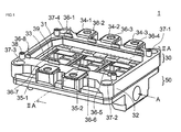
- Fig. 1 is a perspective view of a semiconductor device according to an embodiment of the present invention.
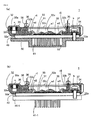
- Fig. 2(a) is a cross-sectional side view of the semiconductor device, taken along the arrow IIA-IIA and viewed from A-side shown in Fig. 1 .
- a semiconductor device 1 has a semiconductor module 30 equipped with power semiconductor chips 31, and a cooler 50 for cooling the power semiconductor chips 31.
- the semiconductor module 30 has at least a surrounding case 32 and an insulating substrate 33 to which the power semiconductor chips 31 are bonded.
- the surrounding case 32 is an O-shaped or frame-shaped resin case that has an approximately rectangular cuboid contour.
- the surrounding case 32 is internally provided with three insulating substrates 33.
- the resin is, for example, polyphenylene sulfide.
- One of the sides of the frame portion of the surrounding case 32 is provided with a main terminal (U) 34-1, a main terminal (V) 34-2, and a main terminal (W) 34-3, and another side of the frame portion is provided with a power supply terminal (P) 35-1 and a power supply terminal (N) 35-2.
- the main terminal (U) 34-1, the main terminal (V) 34-2, and the main terminal (W) 34-3 are terminals for driving, for example, an external motor by performing switching control of the power semiconductor chips 31.
- the power supply terminal (P) 35-1 and the power supply terminal (N) 35-2 are terminals supplied with power from the outside.
- the power supply terminal 35 is provided with an open hole 35a.
- a screw not shown, is inserted into the open hole 35a and then fastened to a nut 32n disposed in the surrounding case 32.
- the power supply terminal 35 bent, is installed on the front surface of the surrounding case 32.
- These terminals are provided to the surrounding case 32 by means of, for example, insert molding.
- Control terminals 36-1 to 36-8 are relay terminals for connecting the gate electrodes of the power semiconductor chips 31 of the surrounding case 32 to a control circuit on a circuit board, not shown, and performing the switching control of the power semiconductor chips 31 in response to a control signal transmitted from the control circuit.
- the four corners of the frame of the surrounding case 32 are provided with openings 37-1 to 37-4. Screws b are inserted into these openings 37-1 to 37-4 to tightly fix the semiconductor module 30 and the cooler 50 to each other.
- the surrounding case 32 is also provided with screw seats 38 for the purpose of attaching the circuit board (not shown) to an upper surface of the surrounding case 32.
- the insulating substrates 33 are each formed by bonding a plate-like circuit pattern made of copper, copper alloy or the like to either surface of a ceramic or resin insulating plate.
- Each of the insulating substrates 33 is mounted with a power semiconductor chip 31 such as an IGBT or MOSFET, and an FWD 39 (Free Wheeling Diode) which is a diode for commutating a load current.
- the plurality of power semiconductor elements 31 and FWDs 39 are connected to each other by a bonding wire w1.
- the power semiconductor chip 31 and the FWD 39 are connected antiparallel to each other, for example, by a bonding wire, not shown, in addition to the bonding wire w1, and are electrically connected so as to configure upper and lower arms.
- lead terminals r1, r2 are insert-molded in the frame portion of the surrounding case 32 and connected to the power semiconductor chips 31 and the like by bonding wires w2, w3.
- Each power semiconductor chip 31 is electrically connected to the motor driving main terminal 34 by a bonding wire, not shown, via the lead terminal, etc.
- the gate of each power semiconductor chip 31 is connected to the lead terminal r2 by the bonding wire w3, and the lead terminal r2 is connected to the control terminal 36.
- the openings on the bottom surface side of the surrounding case 32 have a heat dissipation base that is adhered to opening stepped surfaces 32a by an adhesive to close the openings.
- the heat dissipation base has a heat dissipation base plate 40 and cooling fins 41.
- the heat dissipation base plate 40 is formed from a plate-like member made of or plated with copper, copper alloy, aluminum or aluminum alloy.
- the cooling fins 41 are formed on the lower surface of the heat dissipation base plate 40 by a known method, for the purpose of cooling the heat dissipation base plate 40 and the power semiconductor chips 31.
- Each insulating substrate 33 and the power semiconductor chips 31 thereof are bonded sequentially in this order to the upper surface of the heat dissipation base.
- Such a semiconductor module in which the insulating substrates 33 are bonded to the heat dissipation base is called “direct water-cooled semiconductor module” and is used mainly in a water-cooled semiconductor device that uses water, long life coolant (LLC), or other form of liquid as a coolant.
- LLC long life coolant
- cooling efficiency thereof can be improved by arranging the shapes and positions of the power semiconductor chips 31, the cooling fins 41, and a cooling unit 51, reducing the load on a pump used for circulating the coolant.
- the flow rate of the coolant can be made higher than that in a conventional semiconductor module, improving the properties and reliability of the semiconductor device.
- Fig. 2(b) shows a modification of the heat dissipation base and the semiconductor device 1 using the same.
- the heat dissipation base has at least the heat dissipation base plate 40, a base plate 40-1, and cooling fins 41-1.
- the heat dissipation base plate 40 is adhered to the bottom surface of the surrounding case 32.
- the heat dissipation base plate 40 is not provided with any cooling fins, but the base plate 40-1 having the cooling fins 41-1 implanted therein is tightly fixed to the heat dissipation base plate 40 via a thermal compound or the like.
- the semiconductor module with this heat dissipation base is used mainly in an air-cooled semiconductor device that uses air or other form of gas as a coolant.
- the insulating substrates 33 are soldered or bonded by sintered metal or the like to the upper surface of the heat dissipation base plate 40.
- An internal space of the surrounding case 32 is filled with a sealing member 32e made of silicone gel, silicone resin, or epoxy resin.
- a resin lid plate 32c is tightly adhered to opening stepped surfaces 32b of the surrounding case 32 by an adhesive, not shown, to close the surrounding case 32.
- each opening 37 is provided for the purpose of fixing the surrounding case 32 to the cooler and the like by bolts, as will be described later.
- the semiconductor device 1 is used, with the circuit board, not shown, being attached to the screw seats 38 of the surrounding case 32.
- the front surface of the circuit board is mounted with a control circuit configured by various circuit elements such as an IC (Integrated Circuit), an LSI (Large Scale Integration), a transistor, a resistor, and a capacitor.
- IC Integrated Circuit
- LSI Large Scale Integration
- transistor transistor
- resistor resistor
- capacitor capacitor
- Fig. 3 is a perspective view, schematically showing the principal parts of the semiconductor device according to the embodiment of the present invention, where Fig. 3(a) is a diagram showing an arrangement of the insulating substrates 33, the heat dissipation base, and the cooler 50, and Fig. 3(b) is a diagram showing an arrangement of the cooling fins 41 of the heat dissipation base and the cooler 50.
- the cooler 50 is tightly fixed to the semiconductor module 30 by screws and bolts via a sealing member, as described above, for example.
- the cooler 50 is molded from a known material, such as aluminum or aluminum alloy.
- the cooler 50 has the cooling unit 51 accommodating the cooling fins 41 therein, and a coolant inlet 52 and a coolant outlet 53, which are configured to communicate with the cooling unit 51.
- the cooling unit 51 is an approximately rectangular cuboid concave portion provided in the box-shaped cooler 50, and looks roughly like a rectangle as planarly viewed.
- the coolant inlet 52 and the coolant outlet 53 are formed in such a manner that the centers of the openings thereof are located on the surfaces on the narrow sides of the cooling unit 51, i.e., approximately in the central parts of the two side surfaces of the cooling unit 51 that face each other in the longitudinal direction.
- the openings are in, for example, a circular or oval shape.
- the direction in which the coolant is supplied from the coolant inlet 52 and the direction in which the coolant is discharged from the coolant outlet 53 are roughly parallel to the longitudinal direction of the cooling unit 51.
- a pump Connected to the cooler 50 is a pump, not shown, to supply the coolant from the coolant inlet 52 on the upstream side to the cooling unit 51 and to discharge the coolant from the coolant outlet 53 on the downstream side, creating a cooling system in which the coolant circulates.
- At least two of the insulating substrates 33 are bonded onto the heat dissipation base in such a manner that these insulating substrates 33 are arranged sequentially from the coolant inlet 52 side along the longitudinal direction of the cooling unit 51.
- three insulating substrates 33-1, 33-2, 33-3 in the same contour and size are disposed adjacent to each other from the coolant inlet 52 to the coolant outlet 53.
- the cooling fins 41 are formed on the surface that faces the surface of the heat dissipation base plate 40 to which the insulating substrates 33-1, 33-2, 33-3 are bonded.
- the cooling fins 41 are preferably disposed on a surface immediately below the insulating substrates 33-1, 33-2, 33-3, with a short distance therebetween and hence a low thermal resistance, in such a manner that heat generated by the power semiconductor chips 31 is released efficiently.
- the heat dissipation base is preferably configured in such a manner that the area of the surface of the heat dissipation base plate 40 to which the cooling fins 41 are adhered is greater than the total area of the insulating substrates 33-1, 33-2, 33-3. It is also preferred that the cooler 50 be configured in such a manner that a constant level of gap is formed between the cooling unit 51 and the cooling fins 41.
- the insulating substrates 33-1, 33-2, 33-3 are disposed so as not to be higher than the side walls of the cooling unit 51. In other words, the insulating substrates 33-1, 33-2, 33-3 are disposed in such a manner as to face a coolant flow path configured by the cooling unit 51.
- the cooling fins 41 are a cluster of a plurality of pin members or blade members that has an approximately rectangular cuboid contour.
- the cooling fins 41 are made of copper, copper alloy, aluminum, aluminum alloy, or other known materials and formed on the dissipation base plate 40 by a known method of integral molding, carving, implantation, or the like.
- the length of the edges of the fins or blades measured from the principal surface of the heat dissipation base plate 40 is preferably 6 mm to 10 mm.
- the cooling fins 41 can be in any shapes including the known shapes.
- each of cooling fin 41 have approximately a rectangular cuboid contour so that the virtual plane obtained by connecting the edges thereof becomes substantially parallel to the surface of the heat dissipation base plate 40.
- the inner diameters of the openings of the coolant inlet 52 and the coolant outlet 53 be equal to or greater than the length of the cooling fins 41 in order to keep the cooling performance and reduce pressure loss of the entire cooling system.
- the length of the pins is 10 mm
- pressure loss can be reduced by setting the inner diameters at 10 mm or longer.
- the openings be in an oval shape where the short diameter is equal to or longer than the length of the cooling fins 41 and the long diameter is approximately equivalent to the width of the region where the power semiconductor chips 31 are disposed, so that the coolant spreads over the heat generating portion.
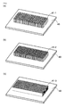
- Fig. 4 is a perspective view illustrating the heat dissipation base according to the embodiment of the present invention, where Fig. 4(a) shows a first modification of the cooling fins, Fig. 4(b) shows a second modification of the cooling fins, and Fig. 4(c) shows a third modification of the cooling fins.
- Fig. 4(a) shows an example in which round pins are used as the cooling fins 41-1
- Fig. 4(b) shows an example in which square pins are used as cooling fins 41-2
- Fig. 4(c) shows an example in which blades are used as cooling fins 41-3.
- the pins be staggered 45° to the longitudinal direction in order to inhibit abnormal flows of the coolant and improve the cooling efficiency.
- Fig. 5 is a cross-sectional diagram of the principal parts of the semiconductor device 1 according to the embodiment of the present invention, taken along the arrow 5A-5A shown in Fig. 3 , where Figs. 5(a) and 5(b) show first and second modifications of the cooler 50, respectively.
- the white arrows in each diagram indicate a direction of the flow of the coolant.
- Fig. 6 is a plan view showing the coolant flow path in the cooler according to the embodiment of the present invention, viewed from the heat dissipation base side, where Figs. 6(a) to 6(d) show first, second, third and fourth modifications of the cooling unit 51, respectively.
- the two-dot chain lines indicate the positions of the insulating substrates 33-1, 33-2, 33-3.
- the cooling unit 51 accommodating the cooling fins 41 therein has a first header part 54 on the coolant inlet 52 side and a second header part 55 on the coolant outlet 53 side.
- the first header part 54 has an enlarged portion with a gradually increasing cross-sectional area, which has a side wall that is inclined in such a manner that the coolant introduced from the coolant inlet 52 into the cooler 50 spreads evenly toward a side plane of the cooling fins 41, and a reduced portion with a gradually reducing cross-sectional area, which accommodates the end portions on one side of the cooling fins 41 therein and has an inclined surface for sending the coolant into the cooling fins 41.
- the bottom surface of the reduced portion of the first header part 54 is inclined toward the bottom plane of the cooling fins 41, i.e., the virtual plane obtained by connecting the edges of the pins or blades.
- the inclination is formed anywhere between a part of the first header part 54 on the coolant inlet 52 side and an end portion of the insulating substrate 33-1 on the coolant outlet 53 side (the position E shown in Figs. 5(a) and 6(a) ).
- the coolant flows through the cooling fins 41 obliquely from not only the side plane of the cooling fins 41 but also the edges of the pins configuring the cooling fins 41, toward the coolant outlet 53, in the direction shown by the dashed arrow shown in Fig. 5 .
- Pressure loss can be reduced by increasing the area of the cooling fins 41 exposed into the first header part 54, which is viewed from the coolant supplied from the coolant inlet 52.
- Pressure loss occurring in the first header part 54 can be limited to a required level by setting the end of the inclined bottom surface within the range described above.
- the second header part 55 has an enlarged portion with a gradually increasing cross-sectional area, which has an inclined surface for discharging the coolant from the cooling fins 41 toward the coolant outlet 53, and a reduced portion with a gradually reducing cross-sectional area, which has a side wall that is inclined in such a manner as to cause the coolant to flow from a side plane of the cooling fins 41 to gather at the coolant outlet 53.
- the bottom surface of the enlarged portion of the second header part 55 is inclined at a position of an end portion of the bottom plane of the cooling fins 41 on the coolant outlet 53 side.
- the angle (acute angle) formed by the bottom surface of the second header part 55 and the bottom plane of the cooling fins 41 is larger than the angle formed by the bottom surface of the first header part 54 and the bottom plane of the cooling fins 41.
- the bottom plane of the cooling unit 51 between the first header part 54 and the second header part 55 is stretched out between the bottom surface of the first header part 54 and the bottom surface of the second header part 55 and is substantially parallel to the bottom plane of the cooling fins 41.
- Providing a predetermined gap between the cooling unit 51 and the cooling fins 41 in this manner can allow the coolant to flow through the cooling fins 41 immediately below the insulating substrates 33-2 and 33-3 disposed on the downstream side of the insulating substrate 33-1, achieving sufficiently high cooling efficiency.
- the shapes of the first header part 54 and the second header part 55 are asymmetric with respect to the cooling unit 51, wherein the volume of the first header part 54 is greater than that of the second header part 55 and the areas of the side plane and bottom plane of the cooling fins 41 on the coolant inlet 52 side that are exposed into the first header part 54 are greater than the area of the side plane of the cooling fins 41 on the coolant outlet 53 side that are exposed into the second header part 55.
- the first semiconductor device 1 has the first header part 54, the cooling unit 51, and the second header part 55, a sufficiently low-temperature coolant can be supplied even to the cooling fins 41 immediately below the insulating substrates 33-2 and 33-3 to efficiently cool the power semiconductor chips 31 mounted in the cooler 50 between the first header part 54 and the second header part 55. Therefore, the power semiconductor chips 31 mounted in the three insulating substrates can be cooled evenly. Even when a pump of the same performance is used, the maximum temperature of the power semiconductor chips 31 can be made lower than that of the prior art, resulting in providing the semiconductor device 1 of excellent cooling performance.
- the effects described above can be obtained favorably by making the area of the bottom plane of the cooling fins 41 exposed into the first header part 54 greater than the area of the side plane of the cooling fins 41 exposed into the first header part 54.
- the shape of the bottom surface of the first header part 54 can be changed in a various manner, as shown in Figs. 6 (a) to 6(d) .
- Fig. 6(a) shows an example of a boundary 57 that appears as a straight top portion (an intersection in the shape of a letter "I") between the bottom surface of the first header part 54 and a surface 56 substantially parallel to the bottom plane of the cooling fins 41.
- the surface 56 substantially parallel to the bottom plane of the cooling fins 41, is positioned between the bottom surface of the first header part 54 and the bottom surface of the second header part 55 and is stretched out thereto.
- Figs. 6(b) to 6(d) each illustrate an example in which the center of the boundary 57 in Fig. 6(a) is curved into a C-shape toward the coolant outlet 53.
- the boundary 57 is located in a section corresponding to the region between center of the insulating substrate 33-1 and its end portion on the coolant outlet 53, i.e., immediately below the region, the insulating substrate 33-1 being shown by a two-dot chain line in the vicinity of the coolant inlet 52. Because the downstream-side end portion of the first header part 54 is curved into a convex C-shape toward the downstream side as shown in Figs. 6(b) to 6(d) , the cooling efficiency in the width direction of the cooling unit 51 can be made further uniform.
- the semiconductor device 1 and the cooler 50 described above can be produced by a conventionally known method.
- Fig. 7 is a cross-sectional diagram showing the principal parts of a conventional semiconductor device. Note, in Fig. 7 , that the same reference numerals are used to indicate the components that are the same as those illustrated in Figs. 1 to 6 , and therefore the descriptions thereof are omitted accordingly.
- the conventional semiconductor device shown in Fig. 7 is different from the semiconductor device 1 according to the embodiment of the present invention that is described with reference to Fig. 5 , in terms of the following features.
- a cooling unit 510 of a cooler 500 does not have the space corresponding to the first header part 54 of the embodiment of present invention.
- the cooling unit 510 does not have the surface 56 parallel to the bottom plane of the cooling fins 41, which is located between the first and second header parts 54 and 55 of the embodiment of the present invention.
- the cooling unit 510 does not have the spaces corresponding to the first and second header parts 54 and 55 of the embodiment of the present invention, and a coolant inlet 520 and a coolant outlet 530 are attached to the bottom portion of the cooling unit 510, unlike the configuration described in the embodiment of the present invention.
- the cooling unit 510 of the cooler 500 has a first header part 540 on the coolant inlet 520 side and a second header part 550 of the same shape and size on the coolant outlet 530 side in such a manner as to be symmetric to the first header part 540.
- the length Iw of the inclined region of the bottom surface of the first header part 540 is approximately equal to the length Ow of the inclined region of the bottom surface of the second header part 550.
- Fig. 8 is a contour diagram showing a numerically calculated distribution of flow velocities of the coolant in the semiconductor device 1 according to the embodiment of the present invention, where Fig. 8(a) is a plan view and Fig. 8(b) is a side view.
- This calculation example is applied mainly to the cooler 50 in which the end portion of the first header part 54 at the position B-B shown in Figs. 8(a) and 8(b) is in the shape of a letter "I.”
- Fig. 9 is a contour diagram showing a numerically calculated distribution of flow velocities of a coolant in the conventional semiconductor device, where Fig. 9(a) is a plan view and Fig. 9(b) is a side view. This calculation example is applied mainly to the cooler 500 shown in Fig. 7(a) .
- Figs. 8 and 9 show the distribution of flow velocities in which the flow rates of the coolant are 10 L/min.
- the numerical values (0.000 to 1.000) shown in these diagrams indicate the flow velocities (unit: m/s) of the coolants.
- the maximum flow velocity is set at 1.000 m/s for the both coolants.
- the semiconductor device 1 When comparing the flow velocity distribution of Fig. 8 according to the embodiment of the present invention with the conventional one shown in Fig. 9 , the semiconductor device 1 according to the embodiment of the present invention has a low flow velocity in the cooling fins 41 at the first header part 54, and the flow velocity changes slowly. Moreover, a substantially uniform distribution is obtained between downstream-side end portion of the first header part 54 (the position B-B shown in Fig. 8 ) and the downstream-side end portion of the cooling fins 41 (the position C-C shown in Fig. 8 ). Therefore, the cooling performance of the cooler 50 is substantially uniform between the coolant inlet 52 and the coolant outlet 53, leading to a reduction in pressure loss.
- the temperature of the chips mounted in the insulating substrate 33-1 on the coolant inlet 52 side was approximately 134.7°C
- the temperature of the chips mounted in the insulating substrate 33-3 on the coolant outlet 53 side was approximately 136.0°C, the difference being approximately 1.3°C.
- the pressure loss was 9.3 kPa.
- the difference between the temperatures was approximately 2.7°C and the pressure loss was 11.1 kPa.
- the semiconductor device 1 according to the embodiment of the present invention can provide the excellent effect of keeping the temperature difference low even after further reducing the length of the cooling fins 41 to as short as, for example, approximately 6 mm.
- the cooling unit 51 of the cooler 50 has the first header part 54, which has at least the bottom surface inclined toward the bottom plane of the cooling fins 41, and the second header part 55, which has at least the bottom surface inclined from the end portion of the bottom plane of the cooling fins 41.
- the coolant supplied from the coolant inlet 52 flows through the cooling fins 41 from the side plane and bottom plane of the cooling fins 41 on the coolant inlet 52 toward the coolant outlet 53, and is then discharged from the side plane of the cooling fins 41 to the coolant outlet 53.
- the pressure loss and cooling efficiency in the first header part 54 can be lowered, resulting in cooling the power semiconductor chips 31 of the three insulating substrates 33 substantially evenly and reducing the pressure loss of the cooler 50, the insulating substrates 33 being disposed in the longitudinal direction of the cooling unit 51.
Landscapes
- Engineering & Computer Science (AREA)
- Physics & Mathematics (AREA)
- Thermal Sciences (AREA)
- Microelectronics & Electronic Packaging (AREA)
- Mechanical Engineering (AREA)
- General Engineering & Computer Science (AREA)
- Cooling Or The Like Of Semiconductors Or Solid State Devices (AREA)
- Chemical & Material Sciences (AREA)
- Materials Engineering (AREA)
Abstract
Description
- The present invention relates to a semiconductor device that has at least a semiconductor module and a cooler, and to the cooler used in this semiconductor device.
- Semiconductor modules with power semiconductor chips are used in the inverters (power converters) of the variable speed drives for the motors of electric vehicles. The elements such as insulated gate bipolar transistors (referred to as "IGBT," hereinafter) are used as the power semiconductor chips. Because the power semiconductor chips generate heat due to high current flowing therein, a semiconductor module is used in combination with a cooler. In electric vehicles and other products with limited weight and space to attach a cooler, a liquid-cooled cooler using a circulatory coolant is used in order to improve the heat dissipation performance of the semiconductor module.
- A semiconductor module has a heat dissipation base that is connected thermally to power semiconductor chips via a substrate, and the heat dissipation base is provided with cooling fins. The cooling fins are accommodated in a flow path formed between the heat dissipation base and a cooler. By letting a pressurized cooling medium (also referred to as "coolant," hereinafter) flow through the cooling fins, heat generated by the semiconductor chips is efficiently released to the cooling medium. The cooling medium that is warmed up by the heat released from the semiconductor chips is cooled by an external heat exchanger, which is then pressurized by a pump and then returned to the flow path in which the cooling fins are disposed.
- This type of conventional technique is disclosed in, for example,
Patent Documents 1 to 5. -
Patent Document 1 discloses a cooling system that has a cooling unit accommodating fins therein, a partial structure that has a cross-sectional flow path that gradually narrows down in the short-side direction of the cooling unit and gradually expands in the long-side direction of the same, and a partial structure that has a cross-sectional flow path that gradually expands from the short side of the cooling unit and gradually narrows down from the long side of the same. Patent Document 2 discloses a cooler that has a parallel flow path configured by a large number of fine flow paths, a first header for distributing a coolant to each flow path of the parallel flow path, and a second header for merging the coolant flowing out of the parallel flow path. Patent Document 3 discloses a cooling device that has a protrusion disposed on an upper surface of a bottom part that configures a bottom surface of a coolant path, wherein the protrusion is configured by an upstream-side upward inclined surface and a downstream-side downward inclined surface. Patent Document 4 discloses a power module cooling unit in which a bottom surface of an opening of a heat sink is provided with a spacer for smoothly reducing the cross-sectional area of a flow path. Patent Document 5 discloses a semiconductor cooling device in which a flow path cover is configured in such a manner that the clearance between the flow path cover and the edges of the pin-shaped fins are wide on the inlet side and narrow on the outlet side. Patent Document 6 discloses a cooling device in which heat transfer fins are configured in such a manner that a coolant is placed higher on the inlet side than on the outlet side. - Patent Document 1: Japanese Patent Application Publication No.
2004-6811 Figs. 1 and7 , paragraphs 0023 to 0031, and 0056 to 0061) - Patent Document 2: Japanese Patent Application Publication No.
2001-35981 Figs. 1 and2 , paragraphs 0020 to 28) - Patent Document 3: Japanese Patent Application Publication No.
2008-263137 - Patent Document 4: Japanese Patent Application Publication No.
2001-308246 Fig. 9 , paragraph 0034) - Patent Document 5: Japanese Patent Application Publication No.
2010-153785 Figs. 7 and8 , paragraphs 0035 to 0037) - Patent Document 6: Japanese Patent Application Publication No.
2007-81375 Figs. 2 ,3 ,6 , and7 , paragraphs 0038 to 0050) - Incidentally, in the semiconductor devices described above, the cooling fins tend to be designed to have detailed and complicated shapes in order to efficiently release the heat generated by the power semiconductor chips. The use of the cooling fins of such shapes is likely to increase pressure loss in the coolers, creating a need for a high-output pump for circulating the coolant. On the other hand, reducing the sizes of the semiconductor devices or configuring the semiconductor devices to provide high outputs, leads to an increase in the amount of heat generated per unit area, creating a need for detailed, dense cooling fins, which results in an increase of pressure loss and creating a need for a large pump.
- In a configuration where a plurality of power semiconductor chips are disposed along the direction in which a coolant flows, it is difficult to cool the chips evenly.
- An object of the present invention, therefore, is to solve these problems and to provide a semiconductor device, whether small or high-output, which is capable of not only keeping its cooling performance with low pressure loss without using a large pump, but also evenly cooling a plurality of power semiconductor chips therein, as well as a cooler used in this semiconductor device.
- In order to solve the problems described above, a semiconductor device according to a first aspect of the present invention is a semiconductor device that has a semiconductor module and a cooler for cooling a power semiconductor element mounted on a substrate in the semiconductor module, the semiconductor device having at least: a heat dissipation base; cooling fins which are a cluster of a plurality of pin members or blade members having an approximately rectangular cuboid contour, and which are provided on a first principal surface of the heat dissipation base; a cooler which is fixed to the heat dissipation base and has a cooling unit accommodating the cooling fins therein and a coolant inlet and a coolant outlet that are formed at respective ends of the cooling unit to face each other in a longitudinal direction; a first substrate which is bonded, in the vicinity of the coolant inlet, to a second principal surface of the heat dissipation base such that the position of the first substrate corresponds to the position of the cooling fins; and a second substrate which is disposed adjacent to the first substrate and bonded, in the vicinity of the coolant outlet, to the second principal surface of the heat dissipation base.
- Furthermore, the cooling unit has: a first header part that has at least a first bottom surface that is inclined toward a bottom plane of the cooling fins so that a coolant supplied from the coolant inlet flows from a side plane and the bottom plane of the cooling fins on the coolant inlet side, into the cooling fins, and toward the coolant outlet; and a second header part that has at least a second bottom surface that is inclined from an end portion of the bottom plane of the cooling fins so that the coolant discharged from the cooling fins flows to the coolant outlet.
- With the first header part and the second header part, the semiconductor device of the present invention can not only cool the power semiconductor elements of the first and second substrates substantially evenly, but also reduce pressure loss of the cooler, the first and second substrates being disposed in the longitudinal direction of the cooling unit.
- In order to solve the problems described above, a semiconductor device according to a second aspect of the present invention is a semiconductor device that has a semiconductor module and a cooler for cooling a power semiconductor element mounted on a substrate in the semiconductor module, the semiconductor device having at least: a heat dissipation base; cooling fins which are a cluster of a plurality of pin members or blade members having an approximately rectangular cuboid contour, and which are provided on a first principal surface of the heat dissipation base; a cooler which is fixed to the heat dissipation base and has a cooling unit accommodating the cooling fins therein and a coolant inlet and a coolant outlet that are formed at respective ends of the cooling unit to face each other in a longitudinal direction; a first substrate which is bonded, in the vicinity of the coolant inlet, to a second principal surface of the heat dissipation base such that the position of the first substrate corresponds to the position of the cooling fins; and a second substrate which is disposed adjacent to the first substrate and bonded, in the vicinity of the coolant outlet, to the second principal surface of the heat dissipation base.
- Furthermore, the cooling unit has: a first header part which has a first bottom surface disposed between the coolant inlet and an end portion of the first substrate on the coolant outlet side and inclined toward a bottom plane of the cooling fins so that a coolant supplied from the coolant inlet flows toward the cooling fins; and a second header part which has a second bottom surface that is inclined from an end portion of the bottom plane of the cooling fins on the coolant outlet side so that the coolant discharged from the cooling fins flows to the coolant outlet.
- With the first header part and the second header part, the semiconductor device of the present invention can not only reduce pressure loss generated between the coolant inlet and the end portion of the first substrate on the coolant outlet side, but also allow the coolant to flow smoothly toward the coolant outlet. As a result, the power semiconductor elements mounted in the first substrate and the second substrate can be cooled substantially evenly, reducing the pressure loss of the cooler.
- In order to solve the problems described above, a semiconductor device according to a third aspect of the present invention is a semiconductor device that has a semiconductor module and a cooler for cooling a power semiconductor element mounted on a substrate in the semiconductor module, the semiconductor device having at least: a heat dissipation base; cooling fins which are a cluster of a plurality of pin members or blade members having an approximately rectangular cuboid contour, and which are provided on a first principal surface of the heat dissipation base; a cooler which is fixed to the heat dissipation base and has a cooling unit accommodating the cooling fins therein and a coolant inlet and a coolant outlet that are formed at respective ends of the cooling unit to face each other in a longitudinal direction; a first substrate which is bonded, in the vicinity of the coolant inlet, to a second principal surface of the heat dissipation base such that the position of the first substrate corresponds to the position of the cooling fins; and a second substrate which is disposed adjacent to the first substrate and bonded, in the vicinity of the coolant outlet, to the second principal surface of the heat dissipation base.
- Furthermore, the cooling unit has: a first header part for supplying a coolant from the coolant inlet toward the cooling fins; and a second header part for discharging the coolant from the cooling fins to the coolant outlet, and the areas of a side plane and a bottom plane of the cooling fins exposed into the first header part are greater than the area of a side plane of the cooling fins exposed to the second header part.
- Because the areas of the side plane and bottom plane of the cooling fins exposed into the first header part are greater than the area of the side plane of the cooling fins exposed to the second header part, the semiconductor of the present invention can cool the power semiconductor chips of the cooler between the first header part and the second header part substantially evenly. Therefore, not only is it possible to reduce pressure loss of the cooler, but also the power semiconductor chips mounted in the first substrate on the first header part side and the power semiconductor chips mounted in the second substrate on the second header side can be cooled substantially evenly.
- Moreover, in order to solve the problems described above, a cooler according to a fourth aspect of the present invention is a cooler for cooling a semiconductor module, which has at least: a heat dissipation base; at least two substrates bonded parallel to each other on the heat dissipation base; a power semiconductor element mounted on each of the substrates; and cooling fins which are a cluster of a plurality of pin members or blade members having an approximately rectangular cuboid contour, and which are provided on the heat dissipation base, the cooler having: a cooling unit accommodating the cooling fins therein; and a coolant inlet and a coolant outlet that are formed at respective ends of the cooling unit to face each other in a longitudinal direction.
- Furthermore, the cooling unit has: a first header part which has at least a first bottom surface that is inclined toward a bottom plane of the cooling fins so that a coolant supplied from the coolant inlet flows from a side plane and the bottom plane of the cooling fins on the coolant inlet side, into the cooling fins, and toward the coolant outlet; and a second header part which has at least a second bottom surface that is inclined from an end portion of the bottom plane of the cooling fins so that the coolant discharged from the cooling fins flows to the coolant outlet. The cooler is used by being fixed to the heat dissipation base.
- With the first header part and the second header part, the cooler of the present invention can not only cool the power semiconductor elements of the first and second substrates substantially evenly, but also reduce pressure loss of the cooler main body, the first and second substrates being disposed in the longitudinal direction of the cooling unit.
- The first to third aspects of the present invention can provide a semiconductor device that is capable of not only cooling the power semiconductor elements of at least two substrates substantially evenly, but also reducing power loss of a cooler of the semiconductor device.
- The fourth aspect of the present invention can provide a cooler that is capable of not only cooling the power semiconductor elements of at least two substrates substantially evenly, but also reducing power loss of the cooler main body.
-
-
Fig. 1 is a perspective view of a semiconductor device according to an embodiment of the present invention; -
Fig. 2(a) is a cross-sectional side view of the semiconductor device according to the embodiment of the present invention, taken along the arrow IIA-IIA and viewed from A-side shown inFig. 1 , andFig. 2(b) shows a modification ofFig. 2(a) ; -
Fig. 3 is a perspective view, schematically showing the principal parts of the semiconductor device according to the embodiment of the present invention, whereFig. 3(a) is a diagram showing a substrate, a heat dissipation base, and a cooler, andFig. 3(b) is a diagram showing cooling fins and the cooler; -
Fig. 4 is a perspective view showing the heat dissipation base according to the embodiment of the present invention, whereFig. 4 (a) is a diagram showing a first modification of the cooling fins,Fig. 4(b) is a diagram showing a second modification of the cooling fins, andFig. 4(c) is a diagram showing a third modification of the cooling fins; -
Fig. 5 is a cross-sectional diagram of the semiconductor device according to the embodiment of the present invention, taken along thearrow 5A-5A shown inFig. 3 , whereFig. 5(a) is a diagram showing a first modification of the cooler, andFig. 5(b) is a diagram showing a second modification of the cooler; -
Fig. 6 is a plan view showing the cooler according to the embodiment of the present invention, whereFig. 6 (a) is a diagram showing a first modification,Fig. 6(b) is a diagram showing a second modification,Fig. 6(c) is a diagram showing a third modification, andFig. 6(d) is a diagram showing a fourth modification; -
Fig. 7 is a cross-sectional diagram showing the principal parts of a conventional semiconductor device; -
Fig. 8 is a contour diagram showing a distribution of flow velocities of a coolant in the semiconductor device according to the embodiment of the present invention, whereFig. 8(a) is a plan view andFig. 8(b) is a side view; and -
Fig. 9 is a contour diagram showing a distribution of flow velocities of a coolant in the conventional semiconductor device, whereFig. 9(a) is a plan view andFig. 9(b) is a side view. - A preferred embodiment of a semiconductor device according to the present invention and a cooler used in this semiconductor device is described hereinafter with reference to the accompanying drawings. The accompanying drawings are provided for the purpose of illustrating the embodiment of the present invention specifically. The terms indicating such directions as "upper," "lower," "bottom," "front," and "back" are used with reference to the directions illustrated in the accompanying drawings.
-
Fig. 1 is a perspective view of a semiconductor device according to an embodiment of the present invention.Fig. 2(a) is a cross-sectional side view of the semiconductor device, taken along the arrow IIA-IIA and viewed from A-side shown inFig. 1 . - As shown in
Figs. 1 and2(a) , asemiconductor device 1 has asemiconductor module 30 equipped withpower semiconductor chips 31, and acooler 50 for cooling thepower semiconductor chips 31. - The
semiconductor module 30 has at least a surroundingcase 32 and aninsulating substrate 33 to which thepower semiconductor chips 31 are bonded. - The surrounding
case 32 is an O-shaped or frame-shaped resin case that has an approximately rectangular cuboid contour. The surroundingcase 32 is internally provided with three insulatingsubstrates 33. The resin is, for example, polyphenylene sulfide. One of the sides of the frame portion of the surroundingcase 32 is provided with a main terminal (U) 34-1, a main terminal (V) 34-2, and a main terminal (W) 34-3, and another side of the frame portion is provided with a power supply terminal (P) 35-1 and a power supply terminal (N) 35-2. The main terminal (U) 34-1, the main terminal (V) 34-2, and the main terminal (W) 34-3 are terminals for driving, for example, an external motor by performing switching control of the power semiconductor chips 31. The power supply terminal (P) 35-1 and the power supply terminal (N) 35-2 are terminals supplied with power from the outside. - As shown in
Fig. 2(a) , thepower supply terminal 35 is provided with anopen hole 35a. A screw, not shown, is inserted into theopen hole 35a and then fastened to anut 32n disposed in the surroundingcase 32. Thepower supply terminal 35, bent, is installed on the front surface of the surroundingcase 32. These terminals are provided to the surroundingcase 32 by means of, for example, insert molding. - Control terminals 36-1 to 36-8 are relay terminals for connecting the gate electrodes of the power semiconductor chips 31 of the surrounding
case 32 to a control circuit on a circuit board, not shown, and performing the switching control of the power semiconductor chips 31 in response to a control signal transmitted from the control circuit. The four corners of the frame of the surroundingcase 32 are provided with openings 37-1 to 37-4. Screws b are inserted into these openings 37-1 to 37-4 to tightly fix thesemiconductor module 30 and the cooler 50 to each other. The surroundingcase 32 is also provided withscrew seats 38 for the purpose of attaching the circuit board (not shown) to an upper surface of the surroundingcase 32. - The insulating
substrates 33 are each formed by bonding a plate-like circuit pattern made of copper, copper alloy or the like to either surface of a ceramic or resin insulating plate. Each of the insulatingsubstrates 33 is mounted with apower semiconductor chip 31 such as an IGBT or MOSFET, and an FWD 39 (Free Wheeling Diode) which is a diode for commutating a load current. The plurality ofpower semiconductor elements 31 andFWDs 39 are connected to each other by a bonding wire w1. In each of the insulatingsubstrates 33, thepower semiconductor chip 31 and theFWD 39 are connected antiparallel to each other, for example, by a bonding wire, not shown, in addition to the bonding wire w1, and are electrically connected so as to configure upper and lower arms. - Furthermore, lead terminals r1, r2 are insert-molded in the frame portion of the surrounding
case 32 and connected to the power semiconductor chips 31 and the like by bonding wires w2, w3. Eachpower semiconductor chip 31 is electrically connected to the motor drivingmain terminal 34 by a bonding wire, not shown, via the lead terminal, etc. The gate of eachpower semiconductor chip 31 is connected to the lead terminal r2 by the bonding wire w3, and the lead terminal r2 is connected to thecontrol terminal 36. - As shown in
Fig. 2 (a) , the openings on the bottom surface side of the surroundingcase 32 have a heat dissipation base that is adhered to opening steppedsurfaces 32a by an adhesive to close the openings. The heat dissipation base has a heatdissipation base plate 40 andcooling fins 41. The heatdissipation base plate 40 is formed from a plate-like member made of or plated with copper, copper alloy, aluminum or aluminum alloy. The coolingfins 41 are formed on the lower surface of the heatdissipation base plate 40 by a known method, for the purpose of cooling the heatdissipation base plate 40 and the power semiconductor chips 31. Each insulatingsubstrate 33 and the power semiconductor chips 31 thereof are bonded sequentially in this order to the upper surface of the heat dissipation base. Such a semiconductor module in which the insulatingsubstrates 33 are bonded to the heat dissipation base is called "direct water-cooled semiconductor module" and is used mainly in a water-cooled semiconductor device that uses water, long life coolant (LLC), or other form of liquid as a coolant. In the direct water-cooled semiconductor module, cooling efficiency thereof can be improved by arranging the shapes and positions of the power semiconductor chips 31, the coolingfins 41, and acooling unit 51, reducing the load on a pump used for circulating the coolant. In addition, the flow rate of the coolant can be made higher than that in a conventional semiconductor module, improving the properties and reliability of the semiconductor device. -
Fig. 2(b) shows a modification of the heat dissipation base and thesemiconductor device 1 using the same. In this modification, the heat dissipation base has at least the heatdissipation base plate 40, a base plate 40-1, and cooling fins 41-1. The heatdissipation base plate 40 is adhered to the bottom surface of the surroundingcase 32. The heatdissipation base plate 40 is not provided with any cooling fins, but the base plate 40-1 having the cooling fins 41-1 implanted therein is tightly fixed to the heatdissipation base plate 40 via a thermal compound or the like. The semiconductor module with this heat dissipation base is used mainly in an air-cooled semiconductor device that uses air or other form of gas as a coolant. - The insulating
substrates 33 are soldered or bonded by sintered metal or the like to the upper surface of the heatdissipation base plate 40. - An internal space of the surrounding
case 32 is filled with a sealingmember 32e made of silicone gel, silicone resin, or epoxy resin. Aresin lid plate 32c is tightly adhered to opening steppedsurfaces 32b of the surroundingcase 32 by an adhesive, not shown, to close the surroundingcase 32. Moreover, each opening 37 is provided for the purpose of fixing the surroundingcase 32 to the cooler and the like by bolts, as will be described later. - The
semiconductor device 1 is used, with the circuit board, not shown, being attached to the screw seats 38 of the surroundingcase 32. The front surface of the circuit board is mounted with a control circuit configured by various circuit elements such as an IC (Integrated Circuit), an LSI (Large Scale Integration), a transistor, a resistor, and a capacitor. Note that thesemiconductor device 1 does not need to have the circuit board therein and therefore may be configured in such a manner as to be controlled while connected to external equipment provided with the same functions. -
Fig. 3 is a perspective view, schematically showing the principal parts of the semiconductor device according to the embodiment of the present invention, whereFig. 3(a) is a diagram showing an arrangement of the insulatingsubstrates 33, the heat dissipation base, and the cooler 50, andFig. 3(b) is a diagram showing an arrangement of the coolingfins 41 of the heat dissipation base and the cooler 50. - The cooler 50 is tightly fixed to the
semiconductor module 30 by screws and bolts via a sealing member, as described above, for example. The cooler 50 is molded from a known material, such as aluminum or aluminum alloy. - As shown in
Fig. 3 , the cooler 50 has the coolingunit 51 accommodating thecooling fins 41 therein, and acoolant inlet 52 and acoolant outlet 53, which are configured to communicate with the coolingunit 51. The coolingunit 51 is an approximately rectangular cuboid concave portion provided in the box-shapedcooler 50, and looks roughly like a rectangle as planarly viewed. Thecoolant inlet 52 and thecoolant outlet 53 are formed in such a manner that the centers of the openings thereof are located on the surfaces on the narrow sides of the coolingunit 51, i.e., approximately in the central parts of the two side surfaces of the coolingunit 51 that face each other in the longitudinal direction. The openings are in, for example, a circular or oval shape. The direction in which the coolant is supplied from thecoolant inlet 52 and the direction in which the coolant is discharged from thecoolant outlet 53 are roughly parallel to the longitudinal direction of the coolingunit 51. - Connected to the cooler 50 is a pump, not shown, to supply the coolant from the
coolant inlet 52 on the upstream side to thecooling unit 51 and to discharge the coolant from thecoolant outlet 53 on the downstream side, creating a cooling system in which the coolant circulates. - At least two of the insulating
substrates 33 are bonded onto the heat dissipation base in such a manner that these insulatingsubstrates 33 are arranged sequentially from thecoolant inlet 52 side along the longitudinal direction of the coolingunit 51. InFig. 3(a) , three insulating substrates 33-1, 33-2, 33-3 in the same contour and size are disposed adjacent to each other from thecoolant inlet 52 to thecoolant outlet 53. - The cooling
fins 41 are formed on the surface that faces the surface of the heatdissipation base plate 40 to which the insulating substrates 33-1, 33-2, 33-3 are bonded. The coolingfins 41 are preferably disposed on a surface immediately below the insulating substrates 33-1, 33-2, 33-3, with a short distance therebetween and hence a low thermal resistance, in such a manner that heat generated by the power semiconductor chips 31 is released efficiently. Because the heat that is generated from the power semiconductor chips 31 spreads in the in-plane direction, the heat dissipation base is preferably configured in such a manner that the area of the surface of the heatdissipation base plate 40 to which thecooling fins 41 are adhered is greater than the total area of the insulating substrates 33-1, 33-2, 33-3. It is also preferred that the cooler 50 be configured in such a manner that a constant level of gap is formed between the coolingunit 51 and the coolingfins 41. The insulating substrates 33-1, 33-2, 33-3 are disposed so as not to be higher than the side walls of the coolingunit 51. In other words, the insulating substrates 33-1, 33-2, 33-3 are disposed in such a manner as to face a coolant flow path configured by the coolingunit 51. - The cooling
fins 41 are a cluster of a plurality of pin members or blade members that has an approximately rectangular cuboid contour. The coolingfins 41 are made of copper, copper alloy, aluminum, aluminum alloy, or other known materials and formed on thedissipation base plate 40 by a known method of integral molding, carving, implantation, or the like. The length of the edges of the fins or blades measured from the principal surface of the heatdissipation base plate 40 is preferably 6 mm to 10 mm. The coolingfins 41 can be in any shapes including the known shapes. In view of achieving uniform cooling performance, it is desired that the height of the pins or the like be made even and that each of coolingfin 41 have approximately a rectangular cuboid contour so that the virtual plane obtained by connecting the edges thereof becomes substantially parallel to the surface of the heatdissipation base plate 40. - It is preferred that the inner diameters of the openings of the
coolant inlet 52 and thecoolant outlet 53 be equal to or greater than the length of the coolingfins 41 in order to keep the cooling performance and reduce pressure loss of the entire cooling system. For example, when the length of the pins is 10 mm, pressure loss can be reduced by setting the inner diameters at 10 mm or longer. From the perspective of the cooling performance, it is also preferred that the openings be in an oval shape where the short diameter is equal to or longer than the length of the coolingfins 41 and the long diameter is approximately equivalent to the width of the region where the power semiconductor chips 31 are disposed, so that the coolant spreads over the heat generating portion. -
Fig. 4 is a perspective view illustrating the heat dissipation base according to the embodiment of the present invention, whereFig. 4(a) shows a first modification of the cooling fins,Fig. 4(b) shows a second modification of the cooling fins, andFig. 4(c) shows a third modification of the cooling fins.Fig. 4(a) shows an example in which round pins are used as the cooling fins 41-1,Fig. 4(b) shows an example in which square pins are used as cooling fins 41-2, andFig. 4(c) shows an example in which blades are used as cooling fins 41-3. When using pins as the cooling fins, it is preferred that the pins be staggered 45° to the longitudinal direction in order to inhibit abnormal flows of the coolant and improve the cooling efficiency. -
Fig. 5 is a cross-sectional diagram of the principal parts of thesemiconductor device 1 according to the embodiment of the present invention, taken along thearrow 5A-5A shown inFig. 3 , whereFigs. 5(a) and 5(b) show first and second modifications of the cooler 50, respectively. The white arrows in each diagram indicate a direction of the flow of the coolant.Fig. 6 is a plan view showing the coolant flow path in the cooler according to the embodiment of the present invention, viewed from the heat dissipation base side, whereFigs. 6(a) to 6(d) show first, second, third and fourth modifications of the coolingunit 51, respectively. The two-dot chain lines indicate the positions of the insulating substrates 33-1, 33-2, 33-3. - In the cooler 50, the cooling
unit 51 accommodating thecooling fins 41 therein has afirst header part 54 on thecoolant inlet 52 side and asecond header part 55 on thecoolant outlet 53 side. - The
first header part 54 has an enlarged portion with a gradually increasing cross-sectional area, which has a side wall that is inclined in such a manner that the coolant introduced from thecoolant inlet 52 into the cooler 50 spreads evenly toward a side plane of the coolingfins 41, and a reduced portion with a gradually reducing cross-sectional area, which accommodates the end portions on one side of the coolingfins 41 therein and has an inclined surface for sending the coolant into the coolingfins 41. - The bottom surface of the reduced portion of the
first header part 54 is inclined toward the bottom plane of the coolingfins 41, i.e., the virtual plane obtained by connecting the edges of the pins or blades. The inclination is formed anywhere between a part of thefirst header part 54 on thecoolant inlet 52 side and an end portion of the insulating substrate 33-1 on thecoolant outlet 53 side (the position E shown inFigs. 5(a) and6(a) ). For the purpose of achieving uniform cooling performance, it is preferred that the inclination be formed anywhere between the center of the insulating substrate 33-1 and the end portion thereof on thecoolant outlet 53. - Owing to such a configuration of the
first header part 54, the coolant flows through the coolingfins 41 obliquely from not only the side plane of the coolingfins 41 but also the edges of the pins configuring the coolingfins 41, toward thecoolant outlet 53, in the direction shown by the dashed arrow shown inFig. 5 . Pressure loss can be reduced by increasing the area of the coolingfins 41 exposed into thefirst header part 54, which is viewed from the coolant supplied from thecoolant inlet 52. Pressure loss occurring in thefirst header part 54 can be limited to a required level by setting the end of the inclined bottom surface within the range described above. - The
second header part 55 has an enlarged portion with a gradually increasing cross-sectional area, which has an inclined surface for discharging the coolant from the coolingfins 41 toward thecoolant outlet 53, and a reduced portion with a gradually reducing cross-sectional area, which has a side wall that is inclined in such a manner as to cause the coolant to flow from a side plane of the coolingfins 41 to gather at thecoolant outlet 53. - The bottom surface of the enlarged portion of the
second header part 55 is inclined at a position of an end portion of the bottom plane of the coolingfins 41 on thecoolant outlet 53 side. The angle (acute angle) formed by the bottom surface of thesecond header part 55 and the bottom plane of the coolingfins 41 is larger than the angle formed by the bottom surface of thefirst header part 54 and the bottom plane of the coolingfins 41. - The bottom plane of the cooling
unit 51 between thefirst header part 54 and thesecond header part 55 is stretched out between the bottom surface of thefirst header part 54 and the bottom surface of thesecond header part 55 and is substantially parallel to the bottom plane of the coolingfins 41. The narrower the gap between this substantially parallel region of the coolingunit 51 and the bottom plane of the coolingfins 41, the greater the cooling performance can be. It is preferred that the gap be, for example, 0.2 mm to 0.8 mm in view of thermal distortion and the like of the heat dissipation base. - Providing a predetermined gap between the cooling
unit 51 and the coolingfins 41 in this manner can allow the coolant to flow through the coolingfins 41 immediately below the insulating substrates 33-2 and 33-3 disposed on the downstream side of the insulating substrate 33-1, achieving sufficiently high cooling efficiency. - The shapes of the
first header part 54 and thesecond header part 55 are asymmetric with respect to thecooling unit 51, wherein the volume of thefirst header part 54 is greater than that of thesecond header part 55 and the areas of the side plane and bottom plane of the coolingfins 41 on thecoolant inlet 52 side that are exposed into thefirst header part 54 are greater than the area of the side plane of the coolingfins 41 on thecoolant outlet 53 side that are exposed into thesecond header part 55. - Because the
first semiconductor device 1 has thefirst header part 54, the coolingunit 51, and thesecond header part 55, a sufficiently low-temperature coolant can be supplied even to the coolingfins 41 immediately below the insulating substrates 33-2 and 33-3 to efficiently cool the power semiconductor chips 31 mounted in the cooler 50 between thefirst header part 54 and thesecond header part 55. Therefore, the power semiconductor chips 31 mounted in the three insulating substrates can be cooled evenly. Even when a pump of the same performance is used, the maximum temperature of the power semiconductor chips 31 can be made lower than that of the prior art, resulting in providing thesemiconductor device 1 of excellent cooling performance. The effects described above can be obtained favorably by making the area of the bottom plane of the coolingfins 41 exposed into thefirst header part 54 greater than the area of the side plane of the coolingfins 41 exposed into thefirst header part 54. - The shape of the bottom surface of the
first header part 54 can be changed in a various manner, as shown inFigs. 6 (a) to 6(d) . -
Fig. 6(a) shows an example of aboundary 57 that appears as a straight top portion (an intersection in the shape of a letter "I") between the bottom surface of thefirst header part 54 and asurface 56 substantially parallel to the bottom plane of the coolingfins 41. Thesurface 56, substantially parallel to the bottom plane of the coolingfins 41, is positioned between the bottom surface of thefirst header part 54 and the bottom surface of thesecond header part 55 and is stretched out thereto.Figs. 6(b) to 6(d) each illustrate an example in which the center of theboundary 57 inFig. 6(a) is curved into a C-shape toward thecoolant outlet 53. In all of these examples, theboundary 57 is located in a section corresponding to the region between center of the insulating substrate 33-1 and its end portion on thecoolant outlet 53, i.e., immediately below the region, the insulating substrate 33-1 being shown by a two-dot chain line in the vicinity of thecoolant inlet 52. Because the downstream-side end portion of thefirst header part 54 is curved into a convex C-shape toward the downstream side as shown inFigs. 6(b) to 6(d) , the cooling efficiency in the width direction of the coolingunit 51 can be made further uniform. - The
semiconductor device 1 and the cooler 50 described above can be produced by a conventionally known method. -
Fig. 7 is a cross-sectional diagram showing the principal parts of a conventional semiconductor device. Note, inFig. 7 , that the same reference numerals are used to indicate the components that are the same as those illustrated inFigs. 1 to 6 , and therefore the descriptions thereof are omitted accordingly. - The conventional semiconductor device shown in
Fig. 7 is different from thesemiconductor device 1 according to the embodiment of the present invention that is described with reference toFig. 5 , in terms of the following features. - For instance, in the semiconductor device shown in
Fig. 7(a) , acooling unit 510 of a cooler 500 does not have the space corresponding to thefirst header part 54 of the embodiment of present invention. In the semiconductor device shown inFig. 7(b) , on the other hand, thecooling unit 510 does not have thesurface 56 parallel to the bottom plane of the coolingfins 41, which is located between the first andsecond header parts Fig. 7(c) , thecooling unit 510 does not have the spaces corresponding to the first andsecond header parts coolant inlet 520 and acoolant outlet 530 are attached to the bottom portion of thecooling unit 510, unlike the configuration described in the embodiment of the present invention. In the semiconductor device shown inFig. 7(d) , thecooling unit 510 of the cooler 500 has afirst header part 540 on thecoolant inlet 520 side and asecond header part 550 of the same shape and size on thecoolant outlet 530 side in such a manner as to be symmetric to thefirst header part 540. The length Iw of the inclined region of the bottom surface of thefirst header part 540 is approximately equal to the length Ow of the inclined region of the bottom surface of thesecond header part 550. -
Fig. 8 is a contour diagram showing a numerically calculated distribution of flow velocities of the coolant in thesemiconductor device 1 according to the embodiment of the present invention, whereFig. 8(a) is a plan view andFig. 8(b) is a side view. This calculation example is applied mainly to the cooler 50 in which the end portion of thefirst header part 54 at the position B-B shown inFigs. 8(a) and 8(b) is in the shape of a letter "I." -
Fig. 9 is a contour diagram showing a numerically calculated distribution of flow velocities of a coolant in the conventional semiconductor device, whereFig. 9(a) is a plan view andFig. 9(b) is a side view. This calculation example is applied mainly to the cooler 500 shown inFig. 7(a) . -
Figs. 8 and9 show the distribution of flow velocities in which the flow rates of the coolant are 10 L/min. The numerical values (0.000 to 1.000) shown in these diagrams indicate the flow velocities (unit: m/s) of the coolants. For comparison, the maximum flow velocity is set at 1.000 m/s for the both coolants. - When comparing the flow velocity distribution of
Fig. 8 according to the embodiment of the present invention with the conventional one shown inFig. 9 , thesemiconductor device 1 according to the embodiment of the present invention has a low flow velocity in the coolingfins 41 at thefirst header part 54, and the flow velocity changes slowly. Moreover, a substantially uniform distribution is obtained between downstream-side end portion of the first header part 54 (the position B-B shown inFig. 8 ) and the downstream-side end portion of the cooling fins 41 (the position C-C shown inFig. 8 ). Therefore, the cooling performance of the cooler 50 is substantially uniform between thecoolant inlet 52 and thecoolant outlet 53, leading to a reduction in pressure loss. - For example, as a result of numerically calculating the junction temperature of the power semiconductor chips 31 mounted in the insulating substrates 33-1, 33-2, 33-3, with the length Iw shown in
Fig. 5 (a) being set at 15 mm, the length Ow at 1 mm, and the length of the coolingfins 41 at 10 mm, the temperature of the chips mounted in the insulating substrate 33-1 on thecoolant inlet 52 side was approximately 134.7°C, and the temperature of the chips mounted in the insulating substrate 33-3 on thecoolant outlet 53 side was approximately 136.0°C, the difference being approximately 1.3°C. In addition, the pressure loss was 9.3 kPa. However, as a result of the same calculation withIw 1 mm and Ow 1mm shown inFig. 7(d) , the difference between the temperatures was approximately 2.7°C and the pressure loss was 11.1 kPa. - In the prior art, reducing the length of the cooling
fins 41 did not evenly cool the plurality of power semiconductor chips 31 disposed in the longitudinal direction, but thesemiconductor device 1 according to the embodiment of the present invention can provide the excellent effect of keeping the temperature difference low even after further reducing the length of the coolingfins 41 to as short as, for example, approximately 6 mm. - Furthermore, as a result of another numerical calculation on the conventional semiconductor device shown in
Fig. 7(d) where the lengths of Iw and Ow were equal to each other and changed from 1 to 5, 10, and 15 mm, it was found that the temperatures of all of the power semiconductor chips mounted in the insulating substrates 33-1, 33-2, 33-3 increased when the length Iw (Ow) was increased from 1 mm to 15 mm, making it impossible to evenly cool the power semiconductor chips. - As described above, in the
semiconductor device 1 and the cooler 50 according to the embodiment of the present invention, the coolingunit 51 of the cooler 50 has thefirst header part 54, which has at least the bottom surface inclined toward the bottom plane of the coolingfins 41, and thesecond header part 55, which has at least the bottom surface inclined from the end portion of the bottom plane of the coolingfins 41. Owing to this configuration, the coolant supplied from thecoolant inlet 52 flows through the coolingfins 41 from the side plane and bottom plane of the coolingfins 41 on thecoolant inlet 52 toward thecoolant outlet 53, and is then discharged from the side plane of the coolingfins 41 to thecoolant outlet 53. As a result, the pressure loss and cooling efficiency in thefirst header part 54 can be lowered, resulting in cooling the power semiconductor chips 31 of the three insulatingsubstrates 33 substantially evenly and reducing the pressure loss of the cooler 50, the insulatingsubstrates 33 being disposed in the longitudinal direction of the coolingunit 51. - It should be noted that the embodiment described above is to illustrate the specific examples of the present invention. Therefore, needless to say, the present invention should not be construed as being limited to the embodiment, and various modifications can be made to the present invention without departing from the gist thereof.
-
- 1
- Semiconductor device
- 30
- Semiconductor module
- 31
- Power semiconductor chip
- 32
- Surrounding case
- 32a, 32b
- Opening stepped surface
- 32c
- Lid plate
- 32e
- Sealing member
- 32n
- Nut
- 33, 33-1, 33-2, 33-3
- Insulating substrate
- 34, 34-1, 34-2, 34-3
- Main terminal
- 35, 35-1, 35-2
- Power supply terminal
- 35a
- Open hole
- 36, 36-1 to 36-8
- Control terminal
- 37, 37-1 to 37-4
- Opening
- 38
- Screw seat
- 39
- FWD
- w1, w2, w3
- Bonding wire
- r1, r2
- Lead terminal
- 40, 40-1
- Heat dissipation base plate
- 41, 41-1, 41-2, 41-3
- Cooling fins
- 50
- Cooler
- 51
- Cooling unit
- 52
- Coolant inlet
- 53
- Coolant outlet
- 54
- First header part
- 55
- Second header part
Claims (15)
- A semiconductor device that has a semiconductor module and a cooler for cooling a power semiconductor element mounted on a substrate in the semiconductor module,
the semiconductor device comprising at least:a heat dissipation base;cooling fins which are a cluster of a plurality of pin members or blade members having an approximately rectangular cuboid contour, and which are provided on a first principal surface of the heat dissipation base;a cooler which is fixed to the heat dissipation base and has a cooling unit accommodating the cooling fins therein and a coolant inlet and a coolant outlet that are formed at respective ends of the cooling unit to face each other in a longitudinal direction;a first substrate which is bonded, in the vicinity of the coolant inlet, to a second principal surface of the heat dissipation base such that the position of the first substrate corresponds to the position of the cooling fins; anda second substrate which is disposed adjacent to the first substrate and bonded, in the vicinity of the coolant outlet, to the second principal surface of the heat dissipation base, whereinthe cooling unit has:a first header part which has at least a first bottom surface that is inclined toward a bottom plane of the cooling fins so that a coolant supplied from the coolant inlet flows from a side plane and the bottom plane of the cooling fins on the coolant inlet side, into the cooling fins, and toward the coolant outlet; and
a second header part which has at least a second bottom surface that is inclined from an end portion of the bottom plane of the cooling fins so that the coolant discharged from the cooling fins flows to the coolant outlet. - A semiconductor device that has a semiconductor module and a cooler for cooling a power semiconductor element mounted on a substrate in the semiconductor module,
the semiconductor device comprising at least:a heat dissipation base;cooling fins which are a cluster of a plurality of pin members or blade members having an approximately rectangular cuboid contour, and which are provided on a first principal surface of the heat dissipation base;a cooler which is fixed to the heat dissipation base, and has a cooling unit accommodating the cooling fins therein and a coolant inlet and a coolant outlet that are formed at respective ends of the cooling unit to face each other in a longitudinal direction;a first substrate which is bonded, in the vicinity of the coolant inlet, to a second principal surface of the heat dissipation base such that the position of the first substrate corresponds to the position of the cooling fins; anda second substrate which is disposed adjacent to the first substrate and bonded, in the vicinity of the coolant outlet, to the second principal surface of the heat dissipation base, whereinthe cooling unit has:a first header part which has a first bottom surface disposed between the coolant inlet and an end portion of the first substrate on the coolant outlet side and inclined toward a bottom plane of the cooling fins so that a coolant supplied from the coolant inlet flows toward the cooling fins; and
a second header part which has a second bottom surface that is inclined from an end portion of the bottom plane of the cooling fins on the coolant outlet side so that the coolant discharged from the cooling fins flows to the coolant outlet. - The semiconductor device according to claim 1 or 2, further comprising a third bottom surface which is stretched out between the first bottom surface and the second bottom surface and parallel to the bottom plane of the cooling fins.
- The semiconductor device according to claim 3, wherein an inclination angle of the first bottom surface with respect to the bottom plane of the cooling fins is smaller than an inclination angle of the second bottom surface.
- The semiconductor device according to claim 4, wherein a top portion in which the first bottom surface and the third bottom surface intersect, is located between a lower part of a center of the first substrate and a lower part of an end portion of the first substrate on the coolant outlet side.
- The semiconductor device according to claim 1 or 2, wherein a volume of the first header part is greater than that of the second header part.
- The semiconductor device according to claim 1 or 2, wherein an inner diameter of a pipe connected to the coolant inlet and the coolant outlet is greater than a length of the pin members or blade members.
- The semiconductor device according to claim 1 or 2, wherein a width of the cooling fins is greater than widths of the first substrate and the second substrate, and a side wall of the cooling unit is not located immediately below the first substrate and the second substrate.
- The semiconductor device according to claim 1 or 2, wherein the pin members each have a circular, oval, or polygonal cross-sectional shape and are staggered on the heat dissipation base.
- A semiconductor device that has a semiconductor module and a cooler for cooling a power semiconductor element mounted on a substrate in the semiconductor module,
the semiconductor device comprising at least:a heat dissipation base;cooling fins which are a cluster of a plurality of pin members or blade members having an approximately rectangular cuboid contour, and which are provided on a first principal surface of the heat dissipation base;a cooler which is fixed to the heat dissipation base and has a cooling unit accommodating the cooling fins therein and a coolant inlet and a coolant outlet that are formed at respective ends of the cooling unit to face each other in a longitudinal direction;a first substrate which is bonded, in the vicinity of the coolant inlet, to a second principal surface of the heat dissipation base such that the position of the first substrate corresponds to the position of the cooling fins; anda second substrate which is disposed adjacent to the first substrate and bonded, in the vicinity of the coolant outlet, to the second principal surface of the heat dissipation base, whereinthe cooling unit has:a first header part for supplying a coolant from the coolant inlet toward the cooling fins; and
a second header part for discharging the coolant from the cooling fins to the coolant outlet, and
areas of a side plane and a bottom plane of the cooling fins exposed into the first header part are greater than an area of a side plane of the cooling fins exposed to the second header part. - The semiconductor device according to claim 10, wherein an area of the bottom plane of the cooling fins exposed into the first header part is greater than an area of the side plane of the cooling fins exposed into the first header part.
- The semiconductor device according to claim 11, wherein a first bottom surface of the first header part is inclined toward the bottom plane of the cooling fins, and a second bottom surface of the second header part is inclined from an end portion of the bottom plane of the cooling fins on the coolant outlet side.
- A cooler for cooling a semiconductor module, which has at least: a heat dissipation base; at least two substrates bonded parallel to each other on the heat dissipation base; a power semiconductor element mounted on each of the substrates; and cooling fins which are a cluster of a plurality of pin members or blade members having an approximately rectangular cuboid contour, and which are provided on the heat dissipation base,
the cooler comprising:a cooling unit accommodating the cooling fins therein; anda coolant inlet and a coolant outlet that are formed at respective ends of the cooling unit to face each other in a longitudinal direction, whereinthe cooling unit has:a first header part which has at least a first bottom surface that is inclined toward a bottom plane of the cooling fins so that a coolant supplied from the coolant inlet flows from a side plane and the bottom plane of the cooling fins on the coolant inlet side, into the cooling fins, and toward the coolant outlet; anda second header part which has at least a second bottom surface that is inclined from an end portion of the bottom plane of the cooling fins so that the coolant discharged from the cooling fins flows to the coolant outlet, andthe cooler is used by being fixed to the heat dissipation base. - The cooler according to claim 13, wherein the substrates include a first substrate disposed on the coolant inlet side and a second substrate disposed on the coolant outlet side so as to be parallel to the first substrate, and wherein the first bottom surface is inclined toward the bottom plane of the cooling fins corresponding to a region between a center of the first substrate and an end portion of the same on the coolant outlet side.
- The cooler according to claim 13, wherein the first header part and the second header part are formed such that an inclination angle of the first bottom surface with respect to the bottom plane of the cooling fins is smaller than an inclination angle of the second bottom surface.
Applications Claiming Priority (2)
| Application Number | Priority Date | Filing Date | Title |
|---|---|---|---|
| JP2012092956 | 2012-04-16 | ||
| PCT/JP2013/060881 WO2013157467A1 (en) | 2012-04-16 | 2013-04-11 | Semiconductor device and cooler for semiconductor device |
Publications (3)
| Publication Number | Publication Date |
|---|---|
| EP2840604A1 true EP2840604A1 (en) | 2015-02-25 |
| EP2840604A4 EP2840604A4 (en) | 2015-12-23 |
| EP2840604B1 EP2840604B1 (en) | 2017-07-19 |
Family
ID=49383426
Family Applications (1)
| Application Number | Title | Priority Date | Filing Date |
|---|---|---|---|
| EP13778515.0A Active EP2840604B1 (en) | 2012-04-16 | 2013-04-11 | Semiconductor device and cooler for semiconductor device |
Country Status (5)
| Country | Link |
|---|---|
| US (1) | US9472488B2 (en) |
| EP (1) | EP2840604B1 (en) |
| JP (1) | JP5900610B2 (en) |
| CN (1) | CN104145333B (en) |
| WO (1) | WO2013157467A1 (en) |
Cited By (1)
| Publication number | Priority date | Publication date | Assignee | Title |
|---|---|---|---|---|
| EP4064336A1 (en) * | 2012-10-29 | 2022-09-28 | Fuji Electric Co., Ltd. | Semiconductor device |
Families Citing this family (77)
| Publication number | Priority date | Publication date | Assignee | Title |
|---|---|---|---|---|
| US9192079B2 (en) * | 2008-09-26 | 2015-11-17 | Rockwell Automation Technologies, Inc. | Power electronic module cooling system and method |
| JP6168152B2 (en) * | 2013-09-05 | 2017-07-26 | 富士電機株式会社 | Power semiconductor module |
| US9646912B2 (en) * | 2013-09-10 | 2017-05-09 | Mitsubishi Electric Corporation | Semiconductor device and semiconductor module having cooling fins |
| WO2015083201A1 (en) * | 2013-12-05 | 2015-06-11 | 三菱電機株式会社 | Power semiconductor device |
| WO2015152373A1 (en) * | 2014-04-03 | 2015-10-08 | 三菱電機株式会社 | Semiconductor device |
| JP6098760B2 (en) * | 2014-05-20 | 2017-03-22 | 富士電機株式会社 | Semiconductor module cooler and manufacturing method thereof |
| TWI590571B (en) * | 2014-12-08 | 2017-07-01 | 強生控制科技公司 | Variable speed drive system and cooling system |
| KR20160128762A (en) * | 2015-04-29 | 2016-11-08 | 주식회사 테라세미콘 | Sealing member |
| US20160338231A1 (en) * | 2015-05-14 | 2016-11-17 | Quantum Fuel Systems Technologies Worldwide, Inc. | Cooling systems and associated methods |
| WO2016194158A1 (en) * | 2015-06-03 | 2016-12-08 | 三菱電機株式会社 | Liquid-cooled cooler, and manufacturing method for radiating fin in liquid-cooled cooler |
| US11218080B2 (en) | 2015-08-31 | 2022-01-04 | Faraday & Future Inc. | Inverter AC bus bar assembly |
| US10135355B2 (en) | 2015-08-31 | 2018-11-20 | Faraday&Future Inc. | Inverter DC bus bar assembly |
| US9241428B1 (en) * | 2015-08-31 | 2016-01-19 | Faraday & Future Inc. | Inverter assembly |
| EP3364870B1 (en) | 2015-10-21 | 2022-09-07 | Neuspera Medical Inc. | Devices and systems for stimulation therapy |
| JP2017084978A (en) * | 2015-10-28 | 2017-05-18 | 株式会社豊田自動織機 | Cooler |
| CN107851633B (en) * | 2016-01-12 | 2021-05-18 | 富士电机株式会社 | semiconductor device |
| WO2017134799A1 (en) * | 2016-02-04 | 2017-08-10 | 三菱電機株式会社 | Semiconductor device |
| EP3236725B8 (en) * | 2016-04-18 | 2020-03-11 | Rolls-Royce plc | Power electronics module |
| JP6920790B2 (en) * | 2016-05-24 | 2021-08-18 | ローム株式会社 | How to assemble intelligent power modules, electric or hybrid vehicles, and intelligent power modules |
| TWI635248B (en) | 2016-09-02 | 2018-09-11 | 宏碁股份有限公司 | Evaporator and manufacturing method thereof |
| JP6750416B2 (en) * | 2016-09-14 | 2020-09-02 | 富士電機株式会社 | Semiconductor module and method of manufacturing semiconductor module |
| DE102016125338B4 (en) * | 2016-12-22 | 2018-07-12 | Rogers Germany Gmbh | System for cooling a carrier substrate and carrier substrate provided for electrical components |
| USD954667S1 (en) | 2017-01-13 | 2022-06-14 | Wolfspeed, Inc. | Power module |
| US11696417B2 (en) | 2017-01-13 | 2023-07-04 | Wolfspeed, Inc. | High power multilayer module having low inductance and fast switching for paralleling power devices |
| US10917992B2 (en) | 2017-01-13 | 2021-02-09 | Cree Fayetteville, Inc. | High power multilayer module having low inductance and fast switching for paralleling power devices |
| US10749443B2 (en) | 2017-01-13 | 2020-08-18 | Cree Fayetteville, Inc. | High power multilayer module having low inductance and fast switching for paralleling power devices |
| US12621969B2 (en) * | 2017-01-20 | 2026-05-05 | Danfoss Silicon Power Gmbh | Electronic power system and method for manufacturing the same |
| WO2018146816A1 (en) * | 2017-02-13 | 2018-08-16 | 新電元工業株式会社 | Electronic device |
| FR3063201B1 (en) * | 2017-02-17 | 2020-03-06 | Valeo Equipements Electriques Moteur | INVERTER OF ROTATING ELECTRIC MACHINE WITH IMPROVED COOLING |
| US10847441B2 (en) * | 2017-03-16 | 2020-11-24 | Mitsubishi Electric Corporation | Cooling system |
| JP6885126B2 (en) * | 2017-03-22 | 2021-06-09 | 富士電機株式会社 | Inverter device |
| DE102017110722B4 (en) * | 2017-05-17 | 2021-03-18 | Semikron Elektronik Gmbh & Co. Kg | Power electronic arrangement and electric vehicle herewith |
| CN107359143A (en) * | 2017-07-17 | 2017-11-17 | 上海道之科技有限公司 | A kind of IGBT module |
| CN111279475B (en) * | 2017-11-01 | 2024-05-28 | 三菱电机株式会社 | Semiconductor device and method for manufacturing the same, and automobile |
| JP6663899B2 (en) * | 2017-11-29 | 2020-03-13 | 本田技研工業株式会社 | Cooling system |
| CN110323273B (en) * | 2018-03-30 | 2025-02-25 | 富士电机株式会社 | Semiconductor device, semiconductor package, semiconductor module and semiconductor circuit device |
| JP7205071B2 (en) | 2018-04-02 | 2023-01-17 | 富士電機株式会社 | Chillers, semiconductor modules and vehicles |
| EP3564992B1 (en) * | 2018-05-02 | 2021-07-07 | EKWB d.o.o. | Fluid-based cooling device for cooling at least two distinct first heat-generating elements of a heat source assembly |
| USD883241S1 (en) * | 2018-06-04 | 2020-05-05 | Semikron Elektronik Gmbh & Co. Kg | Power module |
| JP6493612B1 (en) | 2018-08-13 | 2019-04-03 | 富士電機株式会社 | Power semiconductor module and vehicle |
| USD903590S1 (en) | 2018-09-12 | 2020-12-01 | Cree Fayetteville, Inc. | Power module |
| JP7047929B2 (en) * | 2018-10-03 | 2022-04-05 | 富士電機株式会社 | Semiconductor device |
| US11129310B2 (en) * | 2018-11-22 | 2021-09-21 | Fuji Electric Co., Ltd. | Semiconductor module, vehicle and manufacturing method |
| USD889423S1 (en) * | 2018-12-03 | 2020-07-07 | Semikron Elektronik Gmbh & Co. Kg | Power module |
| CN113767563A (en) * | 2019-01-10 | 2021-12-07 | 沃孚半导体公司 | High power multilayer module with low inductance and fast switching for parallel power devices |
| JP7243262B2 (en) * | 2019-02-15 | 2023-03-22 | 富士電機株式会社 | Semiconductor module, vehicle and manufacturing method |
| DE112019007407T5 (en) * | 2019-05-30 | 2022-02-17 | Mitsubishi Electric Corporation | semiconductor device |
| EP3996133A4 (en) * | 2019-07-02 | 2022-07-13 | Mitsubishi Electric Corporation | POWER MODULE AND METHOD OF MANUFACTURING IT |
| CN113366630B (en) * | 2019-08-06 | 2025-06-24 | 富士电机株式会社 | Semiconductor Modules |
| US11758697B2 (en) | 2019-09-26 | 2023-09-12 | Ohio State Innovation Foundation | Low inductance power module with vertical power loop structure and insulated baseplates |
| US11937403B2 (en) * | 2019-10-23 | 2024-03-19 | Lumentum Operations Llc | Progressive heatsink |
| USD942403S1 (en) * | 2019-10-24 | 2022-02-01 | Wolfspeed, Inc. | Power module having pin fins |
| WO2021166204A2 (en) * | 2020-02-21 | 2021-08-26 | 三菱電機株式会社 | Air conditioning device |
| JP7205662B2 (en) * | 2020-03-18 | 2023-01-17 | 富士電機株式会社 | semiconductor module |
| JP2022095195A (en) * | 2020-12-16 | 2022-06-28 | 日本電産株式会社 | Cooling device |
| JP7080365B1 (en) * | 2021-03-02 | 2022-06-03 | 三菱電機株式会社 | Semiconductor power module |
| CN113035805A (en) * | 2021-03-04 | 2021-06-25 | 阳光电源股份有限公司 | Liquid cooling plate and power module |
| EP4060725B1 (en) * | 2021-03-19 | 2023-07-26 | Hitachi Energy Switzerland AG | A cooling assembly for at least one semiconductor module, a power module and a method for manufacturing a power module |
| US11729944B2 (en) * | 2021-05-21 | 2023-08-15 | Quanta Computer Inc. | Cold plate with anti-clogging mechanism |
| US11877425B2 (en) | 2021-05-28 | 2024-01-16 | Gm Cruise Holdings Llc | Heat spreader with integrated fins |
| JP2023023518A (en) * | 2021-08-05 | 2023-02-16 | 日本電産株式会社 | Liquid cooling jacket and cooling device |
| CN119730149A (en) * | 2021-10-15 | 2025-03-28 | 华为数字能源技术有限公司 | Power supply housing, power supply conversion device and electronic equipment |
| JP2023096940A (en) * | 2021-12-27 | 2023-07-07 | ニデック株式会社 | Heat dissipation material and cooling device |
| JP7111268B1 (en) * | 2022-01-19 | 2022-08-02 | 富士電機株式会社 | Coolers and semiconductor equipment |
| JP7120480B1 (en) * | 2022-01-19 | 2022-08-17 | 富士電機株式会社 | Coolers and semiconductor equipment |
| JPWO2023171529A1 (en) | 2022-03-07 | 2023-09-14 | ||
| US12451817B2 (en) * | 2022-06-02 | 2025-10-21 | Sentec E&E Co., Ltd. | Power module |
| US12622271B2 (en) * | 2022-06-27 | 2026-05-05 | Taiwan Semiconductor Manufacturing Co., Ltd. | Cooling cover and packaged semiconductor device including the same |
| US12213240B2 (en) * | 2022-09-16 | 2025-01-28 | Hamilton Sundstrand Corporation | Pin-fin cooling for printed circuit boards (PCBs) |
| US20240237300A9 (en) * | 2022-10-24 | 2024-07-11 | Strategic Thermal Labs, Llc | Environmentally hardened cold plate for use in liquid cooling of electronic devices |
| CN220274101U (en) * | 2022-12-22 | 2023-12-29 | 华为数字能源技术有限公司 | Cooling devices, power modules, power systems, vehicles and photovoltaic systems |
| US20240365520A1 (en) * | 2023-04-26 | 2024-10-31 | Atieva, Inc. | Thermal device with gradient pin fins for electronics |
| US20240395662A1 (en) * | 2023-05-26 | 2024-11-28 | Semiconductor Components Industries, Llc | Method of direct cooling using a conductive strip |
| CN121400138A (en) * | 2023-07-27 | 2026-01-23 | 三菱电机株式会社 | Power semiconductor device |
| TWD235165S (en) * | 2024-03-05 | 2024-12-01 | 財團法人工業技術研究院 新竹縣竹東鎮中興路四段195號 (中華民國) | Power module housing |
| WO2026013865A1 (en) * | 2024-07-11 | 2026-01-15 | 日産自動車株式会社 | Inverter |
| WO2026048275A1 (en) * | 2024-08-30 | 2026-03-05 | 富士電機株式会社 | Cooler, semiconductor device, and vehicle |
Family Cites Families (27)
| Publication number | Priority date | Publication date | Assignee | Title |
|---|---|---|---|---|
| US4953634A (en) * | 1989-04-20 | 1990-09-04 | Microelectronics And Computer Technology Corporation | Low pressure high heat transfer fluid heat exchanger |
| US5002123A (en) * | 1989-04-20 | 1991-03-26 | Microelectronics And Computer Technology Corporation | Low pressure high heat transfer fluid heat exchanger |
| JPH06326226A (en) | 1993-03-15 | 1994-11-25 | Toshiba Corp | Cooling unit |
| JP2001035981A (en) | 1999-07-16 | 2001-02-09 | Toshiba Corp | Cooler for semiconductor element and power converter using the same |
| US6414867B2 (en) * | 2000-02-16 | 2002-07-02 | Hitachi, Ltd. | Power inverter |
| JP3982180B2 (en) | 2000-02-16 | 2007-09-26 | 株式会社日立製作所 | Power converter |
| JP3800938B2 (en) | 2000-09-13 | 2006-07-26 | 日産自動車株式会社 | Power module cooling device |
| DE10317580B4 (en) * | 2002-04-18 | 2010-09-16 | Hitachi, Ltd. | Electric inverter device with a liquid channel and electric vehicle with such an inverter device |
| JP4138562B2 (en) * | 2002-04-18 | 2008-08-27 | 株式会社日立製作所 | Inverter device for vehicle and electric vehicle equipped with the same |
| JP2004128439A (en) | 2002-08-07 | 2004-04-22 | Fuji Electric Fa Components & Systems Co Ltd | Heating element cooling device |
| JP2007081375A (en) | 2005-08-18 | 2007-03-29 | Matsushita Electric Ind Co Ltd | Cooling system |
| JP4931480B2 (en) | 2006-06-05 | 2012-05-16 | 三洋電機株式会社 | ELECTROCHEMICAL ELEMENT AND ELECTRONIC DEVICE HAVING THE SAME |
| JP5046378B2 (en) * | 2007-03-30 | 2012-10-10 | ニチコン株式会社 | Power semiconductor module and power semiconductor device equipped with the module |
| US7564129B2 (en) | 2007-03-30 | 2009-07-21 | Nichicon Corporation | Power semiconductor module, and power semiconductor device having the module mounted therein |
| JP5155590B2 (en) | 2007-04-13 | 2013-03-06 | 日本インター株式会社 | Cooling system |
| JP5343007B2 (en) * | 2007-11-26 | 2013-11-13 | 株式会社豊田自動織機 | Liquid cooling system |
| US20090145581A1 (en) * | 2007-12-11 | 2009-06-11 | Paul Hoffman | Non-linear fin heat sink |
| JP2010123881A (en) * | 2008-11-21 | 2010-06-03 | Fujikura Ltd | Cold plate |
| JP5381561B2 (en) * | 2008-11-28 | 2014-01-08 | 富士電機株式会社 | Semiconductor cooling device |
| JP3152132U (en) | 2009-04-08 | 2009-07-23 | 奇▲こう▼科技股▲ふん▼有限公司 | Microchannel heat sink device for liquid cooling radiator |
| US8902589B2 (en) * | 2010-04-21 | 2014-12-02 | Fuji Electric Co., Ltd. | Semiconductor module and cooler |
| JP5568026B2 (en) * | 2011-01-20 | 2014-08-06 | トヨタ自動車株式会社 | Brazing method and brazing structure |
| JP5692368B2 (en) * | 2011-04-26 | 2015-04-01 | 富士電機株式会社 | Semiconductor module cooler and semiconductor module |
| CN103890938B (en) * | 2011-10-12 | 2017-10-13 | 富士电机株式会社 | Cooler for semiconductor module and semiconductor module |
| JP2013165096A (en) | 2012-02-09 | 2013-08-22 | Nissan Motor Co Ltd | Semiconductor cooling device |
| JP6093186B2 (en) * | 2013-01-11 | 2017-03-08 | 本田技研工業株式会社 | Semiconductor module cooler |
| JP6227970B2 (en) * | 2013-10-16 | 2017-11-08 | 本田技研工業株式会社 | Semiconductor device |
-
2013
- 2013-04-11 JP JP2014511186A patent/JP5900610B2/en active Active
- 2013-04-11 WO PCT/JP2013/060881 patent/WO2013157467A1/en not_active Ceased
- 2013-04-11 EP EP13778515.0A patent/EP2840604B1/en active Active
- 2013-04-11 CN CN201380012209.3A patent/CN104145333B/en active Active
- 2013-04-11 US US14/374,419 patent/US9472488B2/en active Active
Cited By (1)
| Publication number | Priority date | Publication date | Assignee | Title |
|---|---|---|---|---|
| EP4064336A1 (en) * | 2012-10-29 | 2022-09-28 | Fuji Electric Co., Ltd. | Semiconductor device |
Also Published As
| Publication number | Publication date |
|---|---|
| EP2840604A4 (en) | 2015-12-23 |
| JP5900610B2 (en) | 2016-04-06 |
| CN104145333A (en) | 2014-11-12 |
| EP2840604B1 (en) | 2017-07-19 |
| JPWO2013157467A1 (en) | 2015-12-21 |
| US9472488B2 (en) | 2016-10-18 |
| US20140376184A1 (en) | 2014-12-25 |
| WO2013157467A1 (en) | 2013-10-24 |
| CN104145333B (en) | 2018-02-02 |
Similar Documents
| Publication | Publication Date | Title |
|---|---|---|
| EP2840604B1 (en) | Semiconductor device and cooler for semiconductor device | |
| US9502329B2 (en) | Semiconductor module cooler | |
| CN111211099B (en) | Semiconductor module, vehicle and manufacturing method | |
| JP6315091B2 (en) | Cooler and fixing method of cooler | |
| US11538736B2 (en) | Cooling apparatus, semiconductor module, and vehicle | |
| JP7367394B2 (en) | Semiconductor module, vehicle and manufacturing method | |
| US11456233B2 (en) | Semiconductor module, vehicle and manufacturing method | |
| JP5046378B2 (en) | Power semiconductor module and power semiconductor device equipped with the module | |
| CN113892172B (en) | Semiconductor devices | |
| US12074091B2 (en) | Semiconductor device with cooler including heat dissipating substrate having a plurality of fins bonded to reinforcing plate | |
| JP2013123014A (en) | Semiconductor device | |
| JP6651828B2 (en) | Cooler and power semiconductor module | |
| US20250293119A1 (en) | Cooler and semiconductor apparatus therewith | |
| US12635515B2 (en) | Semiconductor power device, semiconductor power system and method for cooling a semiconductor power device | |
| US20230335456A1 (en) | Semiconductor power device, semiconductor power system and method for cooling a semiconductor power device | |
| US20240379499A1 (en) | Cooler and semiconductor device | |
| TW202543083A (en) | Fluid-cooled power module | |
| WO2026004114A1 (en) | Cooler and semiconductor device | |
| CN119318015A (en) | Power modules with overlapping terminals |
Legal Events
| Date | Code | Title | Description |
|---|---|---|---|
| PUAI | Public reference made under article 153(3) epc to a published international application that has entered the european phase |
Free format text: ORIGINAL CODE: 0009012 |
|
| 17P | Request for examination filed |
Effective date: 20140808 |
|
| AK | Designated contracting states |
Kind code of ref document: A1 Designated state(s): AL AT BE BG CH CY CZ DE DK EE ES FI FR GB GR HR HU IE IS IT LI LT LU LV MC MK MT NL NO PL PT RO RS SE SI SK SM TR |
|
| AX | Request for extension of the european patent |
Extension state: BA ME |
|
| DAX | Request for extension of the european patent (deleted) | ||
| RA4 | Supplementary search report drawn up and despatched (corrected) |
Effective date: 20151124 |
|
| RIC1 | Information provided on ipc code assigned before grant |
Ipc: H01L 25/07 20060101ALI20151118BHEP Ipc: H01L 23/473 20060101AFI20151118BHEP Ipc: H01L 25/18 20060101ALI20151118BHEP |
|
| GRAP | Despatch of communication of intention to grant a patent |
Free format text: ORIGINAL CODE: EPIDOSNIGR1 |
|
| RIC1 | Information provided on ipc code assigned before grant |
Ipc: H01L 23/473 20060101AFI20170111BHEP Ipc: H01L 25/07 20060101ALI20170111BHEP |
|
| INTG | Intention to grant announced |
Effective date: 20170208 |
|
| REG | Reference to a national code |
Ref country code: DE Ref legal event code: R084 Ref document number: 602013023806 Country of ref document: DE |
|
| GRAS | Grant fee paid |
Free format text: ORIGINAL CODE: EPIDOSNIGR3 |
|
| GRAA | (expected) grant |
Free format text: ORIGINAL CODE: 0009210 |
|
| AK | Designated contracting states |
Kind code of ref document: B1 Designated state(s): AL AT BE BG CH CY CZ DE DK EE ES FI FR GB GR HR HU IE IS IT LI LT LU LV MC MK MT NL NO PL PT RO RS SE SI SK SM TR |
|
| REG | Reference to a national code |
Ref country code: GB Ref legal event code: FG4D |
|
| REG | Reference to a national code |
Ref country code: CH Ref legal event code: EP |
|
| REG | Reference to a national code |
Ref country code: IE Ref legal event code: FG4D |
|
| REG | Reference to a national code |
Ref country code: AT Ref legal event code: REF Ref document number: 911137 Country of ref document: AT Kind code of ref document: T Effective date: 20170815 |
|
| REG | Reference to a national code |
Ref country code: DE Ref legal event code: R096 Ref document number: 602013023806 Country of ref document: DE |
|
| REG | Reference to a national code |
Ref country code: NL Ref legal event code: MP Effective date: 20170719 |
|
| REG | Reference to a national code |
Ref country code: LT Ref legal event code: MG4D |
|
| REG | Reference to a national code |
Ref country code: AT Ref legal event code: MK05 Ref document number: 911137 Country of ref document: AT Kind code of ref document: T Effective date: 20170719 |
|
| PG25 | Lapsed in a contracting state [announced via postgrant information from national office to epo] |
Ref country code: SE Free format text: LAPSE BECAUSE OF FAILURE TO SUBMIT A TRANSLATION OF THE DESCRIPTION OR TO PAY THE FEE WITHIN THE PRESCRIBED TIME-LIMIT Effective date: 20170719 Ref country code: NL Free format text: LAPSE BECAUSE OF FAILURE TO SUBMIT A TRANSLATION OF THE DESCRIPTION OR TO PAY THE FEE WITHIN THE PRESCRIBED TIME-LIMIT Effective date: 20170719 Ref country code: HR Free format text: LAPSE BECAUSE OF FAILURE TO SUBMIT A TRANSLATION OF THE DESCRIPTION OR TO PAY THE FEE WITHIN THE PRESCRIBED TIME-LIMIT Effective date: 20170719 Ref country code: LT Free format text: LAPSE BECAUSE OF FAILURE TO SUBMIT A TRANSLATION OF THE DESCRIPTION OR TO PAY THE FEE WITHIN THE PRESCRIBED TIME-LIMIT Effective date: 20170719 Ref country code: NO Free format text: LAPSE BECAUSE OF FAILURE TO SUBMIT A TRANSLATION OF THE DESCRIPTION OR TO PAY THE FEE WITHIN THE PRESCRIBED TIME-LIMIT Effective date: 20171019 Ref country code: AT Free format text: LAPSE BECAUSE OF FAILURE TO SUBMIT A TRANSLATION OF THE DESCRIPTION OR TO PAY THE FEE WITHIN THE PRESCRIBED TIME-LIMIT Effective date: 20170719 Ref country code: FI Free format text: LAPSE BECAUSE OF FAILURE TO SUBMIT A TRANSLATION OF THE DESCRIPTION OR TO PAY THE FEE WITHIN THE PRESCRIBED TIME-LIMIT Effective date: 20170719 |
|
| PG25 | Lapsed in a contracting state [announced via postgrant information from national office to epo] |
Ref country code: PL Free format text: LAPSE BECAUSE OF FAILURE TO SUBMIT A TRANSLATION OF THE DESCRIPTION OR TO PAY THE FEE WITHIN THE PRESCRIBED TIME-LIMIT Effective date: 20170719 Ref country code: IS Free format text: LAPSE BECAUSE OF FAILURE TO SUBMIT A TRANSLATION OF THE DESCRIPTION OR TO PAY THE FEE WITHIN THE PRESCRIBED TIME-LIMIT Effective date: 20171119 Ref country code: ES Free format text: LAPSE BECAUSE OF FAILURE TO SUBMIT A TRANSLATION OF THE DESCRIPTION OR TO PAY THE FEE WITHIN THE PRESCRIBED TIME-LIMIT Effective date: 20170719 Ref country code: LV Free format text: LAPSE BECAUSE OF FAILURE TO SUBMIT A TRANSLATION OF THE DESCRIPTION OR TO PAY THE FEE WITHIN THE PRESCRIBED TIME-LIMIT Effective date: 20170719 Ref country code: BG Free format text: LAPSE BECAUSE OF FAILURE TO SUBMIT A TRANSLATION OF THE DESCRIPTION OR TO PAY THE FEE WITHIN THE PRESCRIBED TIME-LIMIT Effective date: 20171019 Ref country code: RS Free format text: LAPSE BECAUSE OF FAILURE TO SUBMIT A TRANSLATION OF THE DESCRIPTION OR TO PAY THE FEE WITHIN THE PRESCRIBED TIME-LIMIT Effective date: 20170719 Ref country code: GR Free format text: LAPSE BECAUSE OF FAILURE TO SUBMIT A TRANSLATION OF THE DESCRIPTION OR TO PAY THE FEE WITHIN THE PRESCRIBED TIME-LIMIT Effective date: 20171020 |
|
| REG | Reference to a national code |
Ref country code: DE Ref legal event code: R097 Ref document number: 602013023806 Country of ref document: DE |
|
| PG25 | Lapsed in a contracting state [announced via postgrant information from national office to epo] |
Ref country code: DK Free format text: LAPSE BECAUSE OF FAILURE TO SUBMIT A TRANSLATION OF THE DESCRIPTION OR TO PAY THE FEE WITHIN THE PRESCRIBED TIME-LIMIT Effective date: 20170719 Ref country code: CZ Free format text: LAPSE BECAUSE OF FAILURE TO SUBMIT A TRANSLATION OF THE DESCRIPTION OR TO PAY THE FEE WITHIN THE PRESCRIBED TIME-LIMIT Effective date: 20170719 Ref country code: RO Free format text: LAPSE BECAUSE OF FAILURE TO SUBMIT A TRANSLATION OF THE DESCRIPTION OR TO PAY THE FEE WITHIN THE PRESCRIBED TIME-LIMIT Effective date: 20170719 |
|
| PLBE | No opposition filed within time limit |
Free format text: ORIGINAL CODE: 0009261 |
|
| STAA | Information on the status of an ep patent application or granted ep patent |
Free format text: STATUS: NO OPPOSITION FILED WITHIN TIME LIMIT |
|
| PG25 | Lapsed in a contracting state [announced via postgrant information from national office to epo] |
Ref country code: SM Free format text: LAPSE BECAUSE OF FAILURE TO SUBMIT A TRANSLATION OF THE DESCRIPTION OR TO PAY THE FEE WITHIN THE PRESCRIBED TIME-LIMIT Effective date: 20170719 Ref country code: EE Free format text: LAPSE BECAUSE OF FAILURE TO SUBMIT A TRANSLATION OF THE DESCRIPTION OR TO PAY THE FEE WITHIN THE PRESCRIBED TIME-LIMIT Effective date: 20170719 Ref country code: IT Free format text: LAPSE BECAUSE OF FAILURE TO SUBMIT A TRANSLATION OF THE DESCRIPTION OR TO PAY THE FEE WITHIN THE PRESCRIBED TIME-LIMIT Effective date: 20170719 Ref country code: SK Free format text: LAPSE BECAUSE OF FAILURE TO SUBMIT A TRANSLATION OF THE DESCRIPTION OR TO PAY THE FEE WITHIN THE PRESCRIBED TIME-LIMIT Effective date: 20170719 |
|
| 26N | No opposition filed |
Effective date: 20180420 |
|
| PG25 | Lapsed in a contracting state [announced via postgrant information from national office to epo] |
Ref country code: SI Free format text: LAPSE BECAUSE OF FAILURE TO SUBMIT A TRANSLATION OF THE DESCRIPTION OR TO PAY THE FEE WITHIN THE PRESCRIBED TIME-LIMIT Effective date: 20170719 |
|
| PG25 | Lapsed in a contracting state [announced via postgrant information from national office to epo] |
Ref country code: MC Free format text: LAPSE BECAUSE OF FAILURE TO SUBMIT A TRANSLATION OF THE DESCRIPTION OR TO PAY THE FEE WITHIN THE PRESCRIBED TIME-LIMIT Effective date: 20170719 |
|
| REG | Reference to a national code |
Ref country code: CH Ref legal event code: PL |
|
| REG | Reference to a national code |
Ref country code: BE Ref legal event code: MM Effective date: 20180430 |
|
| GBPC | Gb: european patent ceased through non-payment of renewal fee |
Effective date: 20180411 |
|
| REG | Reference to a national code |
Ref country code: IE Ref legal event code: MM4A |
|
| PG25 | Lapsed in a contracting state [announced via postgrant information from national office to epo] |
Ref country code: LU Free format text: LAPSE BECAUSE OF NON-PAYMENT OF DUE FEES Effective date: 20180411 |
|
| PG25 | Lapsed in a contracting state [announced via postgrant information from national office to epo] |
Ref country code: BE Free format text: LAPSE BECAUSE OF NON-PAYMENT OF DUE FEES Effective date: 20180430 Ref country code: CH Free format text: LAPSE BECAUSE OF NON-PAYMENT OF DUE FEES Effective date: 20180430 Ref country code: GB Free format text: LAPSE BECAUSE OF NON-PAYMENT OF DUE FEES Effective date: 20180411 Ref country code: LI Free format text: LAPSE BECAUSE OF NON-PAYMENT OF DUE FEES Effective date: 20180430 |
|
| PG25 | Lapsed in a contracting state [announced via postgrant information from national office to epo] |
Ref country code: IE Free format text: LAPSE BECAUSE OF NON-PAYMENT OF DUE FEES Effective date: 20180411 Ref country code: FR Free format text: LAPSE BECAUSE OF NON-PAYMENT OF DUE FEES Effective date: 20180430 |
|
| PG25 | Lapsed in a contracting state [announced via postgrant information from national office to epo] |
Ref country code: MT Free format text: LAPSE BECAUSE OF NON-PAYMENT OF DUE FEES Effective date: 20180411 |
|
| PG25 | Lapsed in a contracting state [announced via postgrant information from national office to epo] |
Ref country code: TR Free format text: LAPSE BECAUSE OF FAILURE TO SUBMIT A TRANSLATION OF THE DESCRIPTION OR TO PAY THE FEE WITHIN THE PRESCRIBED TIME-LIMIT Effective date: 20170719 |
|
| PG25 | Lapsed in a contracting state [announced via postgrant information from national office to epo] |
Ref country code: PT Free format text: LAPSE BECAUSE OF FAILURE TO SUBMIT A TRANSLATION OF THE DESCRIPTION OR TO PAY THE FEE WITHIN THE PRESCRIBED TIME-LIMIT Effective date: 20170719 Ref country code: HU Free format text: LAPSE BECAUSE OF FAILURE TO SUBMIT A TRANSLATION OF THE DESCRIPTION OR TO PAY THE FEE WITHIN THE PRESCRIBED TIME-LIMIT; INVALID AB INITIO Effective date: 20130411 |
|
| PG25 | Lapsed in a contracting state [announced via postgrant information from national office to epo] |
Ref country code: MK Free format text: LAPSE BECAUSE OF NON-PAYMENT OF DUE FEES Effective date: 20170719 Ref country code: CY Free format text: LAPSE BECAUSE OF FAILURE TO SUBMIT A TRANSLATION OF THE DESCRIPTION OR TO PAY THE FEE WITHIN THE PRESCRIBED TIME-LIMIT Effective date: 20170719 |
|
| PG25 | Lapsed in a contracting state [announced via postgrant information from national office to epo] |
Ref country code: AL Free format text: LAPSE BECAUSE OF FAILURE TO SUBMIT A TRANSLATION OF THE DESCRIPTION OR TO PAY THE FEE WITHIN THE PRESCRIBED TIME-LIMIT Effective date: 20170719 |
|
| PGFP | Annual fee paid to national office [announced via postgrant information from national office to epo] |
Ref country code: DE Payment date: 20250305 Year of fee payment: 13 |
|
| REG | Reference to a national code |
Ref country code: DE Ref legal event code: R079 Ref document number: 602013023806 Country of ref document: DE Free format text: PREVIOUS MAIN CLASS: H01L0023473000 Ipc: H10W0040470000 |