EP2831922B1 - Modules photovoltaïques comportant des milieux orientant la lumière et procédés pour leur fabrication - Google Patents
Modules photovoltaïques comportant des milieux orientant la lumière et procédés pour leur fabrication Download PDFInfo
- Publication number
- EP2831922B1 EP2831922B1 EP13769124.2A EP13769124A EP2831922B1 EP 2831922 B1 EP2831922 B1 EP 2831922B1 EP 13769124 A EP13769124 A EP 13769124A EP 2831922 B1 EP2831922 B1 EP 2831922B1
- Authority
- EP
- European Patent Office
- Prior art keywords
- light directing
- photovoltaic
- electrical connector
- directing medium
- adhesive
- Prior art date
- Legal status (The legal status is an assumption and is not a legal conclusion. Google has not performed a legal analysis and makes no representation as to the accuracy of the status listed.)
- Active
Links
- 238000000034 method Methods 0.000 title claims description 11
- 239000000853 adhesive Substances 0.000 claims description 24
- 230000001070 adhesive effect Effects 0.000 claims description 24
- 239000010410 layer Substances 0.000 claims description 23
- 238000000576 coating method Methods 0.000 claims description 20
- 239000011248 coating agent Substances 0.000 claims description 16
- 238000010276 construction Methods 0.000 claims description 13
- 229920005989 resin Polymers 0.000 claims description 10
- 239000011347 resin Substances 0.000 claims description 10
- 239000013047 polymeric layer Substances 0.000 claims description 8
- 238000010438 heat treatment Methods 0.000 claims description 7
- 238000004519 manufacturing process Methods 0.000 claims description 5
- 239000008393 encapsulating agent Substances 0.000 description 20
- 239000011521 glass Substances 0.000 description 13
- 239000004820 Pressure-sensitive adhesive Substances 0.000 description 10
- NIXOWILDQLNWCW-UHFFFAOYSA-N acrylic acid group Chemical group C(C=C)(=O)O NIXOWILDQLNWCW-UHFFFAOYSA-N 0.000 description 7
- 239000010408 film Substances 0.000 description 7
- 239000000463 material Substances 0.000 description 7
- 239000004831 Hot glue Substances 0.000 description 6
- XEEYBQQBJWHFJM-UHFFFAOYSA-N Iron Chemical compound [Fe] XEEYBQQBJWHFJM-UHFFFAOYSA-N 0.000 description 6
- NIXOWILDQLNWCW-UHFFFAOYSA-M acrylate group Chemical group C(C=C)(=O)[O-] NIXOWILDQLNWCW-UHFFFAOYSA-M 0.000 description 6
- 239000000203 mixture Substances 0.000 description 6
- 239000005038 ethylene vinyl acetate Substances 0.000 description 5
- 239000000178 monomer Substances 0.000 description 5
- 229920000098 polyolefin Polymers 0.000 description 5
- HRPVXLWXLXDGHG-UHFFFAOYSA-N Acrylamide Chemical compound NC(=O)C=C HRPVXLWXLXDGHG-UHFFFAOYSA-N 0.000 description 4
- 150000001875 compounds Chemical group 0.000 description 4
- 229910052751 metal Inorganic materials 0.000 description 4
- 239000002184 metal Substances 0.000 description 4
- 229920001200 poly(ethylene-vinyl acetate) Polymers 0.000 description 4
- VYPSYNLAJGMNEJ-UHFFFAOYSA-N silicon dioxide Inorganic materials O=[Si]=O VYPSYNLAJGMNEJ-UHFFFAOYSA-N 0.000 description 4
- 238000005476 soldering Methods 0.000 description 4
- RYGMFSIKBFXOCR-UHFFFAOYSA-N Copper Chemical compound [Cu] RYGMFSIKBFXOCR-UHFFFAOYSA-N 0.000 description 3
- DQXBYHZEEUGOBF-UHFFFAOYSA-N but-3-enoic acid;ethene Chemical compound C=C.OC(=O)CC=C DQXBYHZEEUGOBF-UHFFFAOYSA-N 0.000 description 3
- 238000006243 chemical reaction Methods 0.000 description 3
- 229910052742 iron Inorganic materials 0.000 description 3
- 229920003229 poly(methyl methacrylate) Polymers 0.000 description 3
- 229920000647 polyepoxide Polymers 0.000 description 3
- -1 polyethylene Polymers 0.000 description 3
- 229920001169 thermoplastic Polymers 0.000 description 3
- VZCYOOQTPOCHFL-UHFFFAOYSA-N trans-butenedioic acid Natural products OC(=O)C=CC(O)=O VZCYOOQTPOCHFL-UHFFFAOYSA-N 0.000 description 3
- 239000004593 Epoxy Substances 0.000 description 2
- VZCYOOQTPOCHFL-OWOJBTEDSA-N Fumaric acid Chemical compound OC(=O)\C=C\C(O)=O VZCYOOQTPOCHFL-OWOJBTEDSA-N 0.000 description 2
- CERQOIWHTDAKMF-UHFFFAOYSA-N Methacrylic acid Chemical compound CC(=C)C(O)=O CERQOIWHTDAKMF-UHFFFAOYSA-N 0.000 description 2
- 241000276498 Pollachius virens Species 0.000 description 2
- BQCADISMDOOEFD-UHFFFAOYSA-N Silver Chemical compound [Ag] BQCADISMDOOEFD-UHFFFAOYSA-N 0.000 description 2
- 150000001252 acrylic acid derivatives Chemical class 0.000 description 2
- 229910021417 amorphous silicon Inorganic materials 0.000 description 2
- 230000004888 barrier function Effects 0.000 description 2
- 230000005540 biological transmission Effects 0.000 description 2
- 229910052802 copper Inorganic materials 0.000 description 2
- 239000010949 copper Substances 0.000 description 2
- 229910021419 crystalline silicon Inorganic materials 0.000 description 2
- 230000007613 environmental effect Effects 0.000 description 2
- 125000003700 epoxy group Chemical group 0.000 description 2
- 239000002803 fossil fuel Substances 0.000 description 2
- 239000000446 fuel Substances 0.000 description 2
- 229920000554 ionomer Polymers 0.000 description 2
- VZCYOOQTPOCHFL-UPHRSURJSA-N maleic acid Chemical compound OC(=O)\C=C/C(O)=O VZCYOOQTPOCHFL-UPHRSURJSA-N 0.000 description 2
- 238000013086 organic photovoltaic Methods 0.000 description 2
- 229920002037 poly(vinyl butyral) polymer Polymers 0.000 description 2
- 229920000728 polyester Polymers 0.000 description 2
- 229920000139 polyethylene terephthalate Polymers 0.000 description 2
- 239000005020 polyethylene terephthalate Substances 0.000 description 2
- 239000002861 polymer material Substances 0.000 description 2
- 239000010453 quartz Substances 0.000 description 2
- 230000005855 radiation Effects 0.000 description 2
- 230000000630 rising effect Effects 0.000 description 2
- 239000000377 silicon dioxide Substances 0.000 description 2
- 229910052709 silver Inorganic materials 0.000 description 2
- 239000004332 silver Substances 0.000 description 2
- ISXSCDLOGDJUNJ-UHFFFAOYSA-N tert-butyl prop-2-enoate Chemical compound CC(C)(C)OC(=O)C=C ISXSCDLOGDJUNJ-UHFFFAOYSA-N 0.000 description 2
- 229920001187 thermosetting polymer Polymers 0.000 description 2
- 239000004416 thermosoftening plastic Substances 0.000 description 2
- PSGCQDPCAWOCSH-UHFFFAOYSA-N (4,7,7-trimethyl-3-bicyclo[2.2.1]heptanyl) prop-2-enoate Chemical compound C1CC2(C)C(OC(=O)C=C)CC1C2(C)C PSGCQDPCAWOCSH-UHFFFAOYSA-N 0.000 description 1
- JWYVGKFDLWWQJX-UHFFFAOYSA-N 1-ethenylazepan-2-one Chemical compound C=CN1CCCCCC1=O JWYVGKFDLWWQJX-UHFFFAOYSA-N 0.000 description 1
- LMAUULKNZLEMGN-UHFFFAOYSA-N 1-ethyl-3,5-dimethylbenzene Chemical compound CCC1=CC(C)=CC(C)=C1 LMAUULKNZLEMGN-UHFFFAOYSA-N 0.000 description 1
- SMZOUWXMTYCWNB-UHFFFAOYSA-N 2-(2-methoxy-5-methylphenyl)ethanamine Chemical compound COC1=CC=C(C)C=C1CCN SMZOUWXMTYCWNB-UHFFFAOYSA-N 0.000 description 1
- JAHNSTQSQJOJLO-UHFFFAOYSA-N 2-(3-fluorophenyl)-1h-imidazole Chemical compound FC1=CC=CC(C=2NC=CN=2)=C1 JAHNSTQSQJOJLO-UHFFFAOYSA-N 0.000 description 1
- GOXQRTZXKQZDDN-UHFFFAOYSA-N 2-Ethylhexyl acrylate Chemical compound CCCCC(CC)COC(=O)C=C GOXQRTZXKQZDDN-UHFFFAOYSA-N 0.000 description 1
- 229940095095 2-hydroxyethyl acrylate Drugs 0.000 description 1
- 229940044192 2-hydroxyethyl methacrylate Drugs 0.000 description 1
- OMIGHNLMNHATMP-UHFFFAOYSA-N 2-hydroxyethyl prop-2-enoate Chemical compound OCCOC(=O)C=C OMIGHNLMNHATMP-UHFFFAOYSA-N 0.000 description 1
- NCTBYWFEJFTVEL-UHFFFAOYSA-N 2-methylbutyl prop-2-enoate Chemical compound CCC(C)COC(=O)C=C NCTBYWFEJFTVEL-UHFFFAOYSA-N 0.000 description 1
- ZVYGIPWYVVJFRW-UHFFFAOYSA-N 3-methylbutyl prop-2-enoate Chemical compound CC(C)CCOC(=O)C=C ZVYGIPWYVVJFRW-UHFFFAOYSA-N 0.000 description 1
- ATVJXMYDOSMEPO-UHFFFAOYSA-N 3-prop-2-enoxyprop-1-ene Chemical compound C=CCOCC=C ATVJXMYDOSMEPO-UHFFFAOYSA-N 0.000 description 1
- BVDBXCXQMHBGQM-UHFFFAOYSA-N 4-methylpentan-2-yl prop-2-enoate Chemical compound CC(C)CC(C)OC(=O)C=C BVDBXCXQMHBGQM-UHFFFAOYSA-N 0.000 description 1
- DXPPIEDUBFUSEZ-UHFFFAOYSA-N 6-methylheptyl prop-2-enoate Chemical compound CC(C)CCCCCOC(=O)C=C DXPPIEDUBFUSEZ-UHFFFAOYSA-N 0.000 description 1
- CUXGDKOCSSIRKK-UHFFFAOYSA-N 7-methyloctyl prop-2-enoate Chemical compound CC(C)CCCCCCOC(=O)C=C CUXGDKOCSSIRKK-UHFFFAOYSA-N 0.000 description 1
- GYHNNYVSQQEPJS-UHFFFAOYSA-N Gallium Chemical compound [Ga] GYHNNYVSQQEPJS-UHFFFAOYSA-N 0.000 description 1
- CERQOIWHTDAKMF-UHFFFAOYSA-M Methacrylate Chemical compound CC(=C)C([O-])=O CERQOIWHTDAKMF-UHFFFAOYSA-M 0.000 description 1
- 241000428199 Mustelinae Species 0.000 description 1
- WHNWPMSKXPGLAX-UHFFFAOYSA-N N-Vinyl-2-pyrrolidone Chemical compound C=CN1CCCC1=O WHNWPMSKXPGLAX-UHFFFAOYSA-N 0.000 description 1
- 239000004698 Polyethylene Substances 0.000 description 1
- 229920002367 Polyisobutene Polymers 0.000 description 1
- 239000004743 Polypropylene Substances 0.000 description 1
- OFOBLEOULBTSOW-UHFFFAOYSA-N Propanedioic acid Natural products OC(=O)CC(O)=O OFOBLEOULBTSOW-UHFFFAOYSA-N 0.000 description 1
- XUIMIQQOPSSXEZ-UHFFFAOYSA-N Silicon Chemical compound [Si] XUIMIQQOPSSXEZ-UHFFFAOYSA-N 0.000 description 1
- QYKIQEUNHZKYBP-UHFFFAOYSA-N Vinyl ether Chemical compound C=COC=C QYKIQEUNHZKYBP-UHFFFAOYSA-N 0.000 description 1
- IQTMWNQRJYAGDL-UHFFFAOYSA-N [SeH2]=[Se] Chemical compound [SeH2]=[Se] IQTMWNQRJYAGDL-UHFFFAOYSA-N 0.000 description 1
- 229920006397 acrylic thermoplastic Polymers 0.000 description 1
- 229910052782 aluminium Inorganic materials 0.000 description 1
- XAGFODPZIPBFFR-UHFFFAOYSA-N aluminium Chemical compound [Al] XAGFODPZIPBFFR-UHFFFAOYSA-N 0.000 description 1
- 238000005452 bending Methods 0.000 description 1
- 230000015572 biosynthetic process Effects 0.000 description 1
- 239000004566 building material Substances 0.000 description 1
- 235000013877 carbamide Nutrition 0.000 description 1
- 239000000919 ceramic Substances 0.000 description 1
- 239000004020 conductor Substances 0.000 description 1
- 238000001816 cooling Methods 0.000 description 1
- HVMJUDPAXRRVQO-UHFFFAOYSA-N copper indium Chemical compound [Cu].[In] HVMJUDPAXRRVQO-UHFFFAOYSA-N 0.000 description 1
- 238000005336 cracking Methods 0.000 description 1
- 239000003431 cross linking reagent Substances 0.000 description 1
- KBLWLMPSVYBVDK-UHFFFAOYSA-N cyclohexyl prop-2-enoate Chemical compound C=CC(=O)OC1CCCCC1 KBLWLMPSVYBVDK-UHFFFAOYSA-N 0.000 description 1
- 230000007423 decrease Effects 0.000 description 1
- FWLDHHJLVGRRHD-UHFFFAOYSA-N decyl prop-2-enoate Chemical compound CCCCCCCCCCOC(=O)C=C FWLDHHJLVGRRHD-UHFFFAOYSA-N 0.000 description 1
- 230000007812 deficiency Effects 0.000 description 1
- 239000012777 electrically insulating material Substances 0.000 description 1
- 238000005265 energy consumption Methods 0.000 description 1
- 238000005516 engineering process Methods 0.000 description 1
- 239000003822 epoxy resin Substances 0.000 description 1
- 229920002313 fluoropolymer Polymers 0.000 description 1
- 239000004811 fluoropolymer Substances 0.000 description 1
- 238000009472 formulation Methods 0.000 description 1
- 239000001530 fumaric acid Substances 0.000 description 1
- 229910052733 gallium Inorganic materials 0.000 description 1
- LNEPOXFFQSENCJ-UHFFFAOYSA-N haloperidol Chemical compound C1CC(O)(C=2C=CC(Cl)=CC=2)CCN1CCCC(=O)C1=CC=C(F)C=C1 LNEPOXFFQSENCJ-UHFFFAOYSA-N 0.000 description 1
- 238000011065 in-situ storage Methods 0.000 description 1
- 239000000976 ink Substances 0.000 description 1
- 239000012948 isocyanate Chemical class 0.000 description 1
- 150000002513 isocyanates Chemical class 0.000 description 1
- 238000003475 lamination Methods 0.000 description 1
- PBOSTUDLECTMNL-UHFFFAOYSA-N lauryl acrylate Chemical compound CCCCCCCCCCCCOC(=O)C=C PBOSTUDLECTMNL-UHFFFAOYSA-N 0.000 description 1
- 239000011976 maleic acid Substances 0.000 description 1
- 239000011159 matrix material Substances 0.000 description 1
- 239000012528 membrane Substances 0.000 description 1
- 150000002734 metacrylic acid derivatives Chemical class 0.000 description 1
- 238000001465 metallisation Methods 0.000 description 1
- 150000002739 metals Chemical class 0.000 description 1
- FQPSGWSUVKBHSU-UHFFFAOYSA-N methacrylamide Chemical compound CC(=C)C(N)=O FQPSGWSUVKBHSU-UHFFFAOYSA-N 0.000 description 1
- 125000005395 methacrylic acid group Chemical group 0.000 description 1
- LVHBHZANLOWSRM-UHFFFAOYSA-N methylenebutanedioic acid Natural products OC(=O)CC(=C)C(O)=O LVHBHZANLOWSRM-UHFFFAOYSA-N 0.000 description 1
- 229940088644 n,n-dimethylacrylamide Drugs 0.000 description 1
- YLGYACDQVQQZSW-UHFFFAOYSA-N n,n-dimethylprop-2-enamide Chemical compound CN(C)C(=O)C=C YLGYACDQVQQZSW-UHFFFAOYSA-N 0.000 description 1
- UUORTJUPDJJXST-UHFFFAOYSA-N n-(2-hydroxyethyl)prop-2-enamide Chemical compound OCCNC(=O)C=C UUORTJUPDJJXST-UHFFFAOYSA-N 0.000 description 1
- SWPMNMYLORDLJE-UHFFFAOYSA-N n-ethylprop-2-enamide Chemical compound CCNC(=O)C=C SWPMNMYLORDLJE-UHFFFAOYSA-N 0.000 description 1
- AWGZKFQMWZYCHF-UHFFFAOYSA-N n-octylprop-2-enamide Chemical compound CCCCCCCCNC(=O)C=C AWGZKFQMWZYCHF-UHFFFAOYSA-N 0.000 description 1
- XFHJDMUEHUHAJW-UHFFFAOYSA-N n-tert-butylprop-2-enamide Chemical compound CC(C)(C)NC(=O)C=C XFHJDMUEHUHAJW-UHFFFAOYSA-N 0.000 description 1
- 230000003287 optical effect Effects 0.000 description 1
- 239000002245 particle Substances 0.000 description 1
- 230000000704 physical effect Effects 0.000 description 1
- 229920000058 polyacrylate Polymers 0.000 description 1
- 229920000570 polyether Polymers 0.000 description 1
- 229920000573 polyethylene Polymers 0.000 description 1
- 229920000642 polymer Polymers 0.000 description 1
- 229920006254 polymer film Polymers 0.000 description 1
- 229920001155 polypropylene Polymers 0.000 description 1
- 229920001296 polysiloxane Polymers 0.000 description 1
- 239000004810 polytetrafluoroethylene Substances 0.000 description 1
- 229920001343 polytetrafluoroethylene Polymers 0.000 description 1
- 239000004800 polyvinyl chloride Substances 0.000 description 1
- 229920000915 polyvinyl chloride Polymers 0.000 description 1
- 230000001012 protector Effects 0.000 description 1
- 150000003254 radicals Chemical class 0.000 description 1
- 238000002310 reflectometry Methods 0.000 description 1
- 239000012783 reinforcing fiber Substances 0.000 description 1
- 238000007650 screen-printing Methods 0.000 description 1
- 239000000565 sealant Substances 0.000 description 1
- 229910052710 silicon Inorganic materials 0.000 description 1
- 239000010703 silicon Substances 0.000 description 1
- 229910000679 solder Inorganic materials 0.000 description 1
- 239000007787 solid Substances 0.000 description 1
- 229920002803 thermoplastic polyurethane Polymers 0.000 description 1
- 239000010409 thin film Substances 0.000 description 1
- 150000003672 ureas Chemical class 0.000 description 1
- 150000003673 urethanes Chemical class 0.000 description 1
- 239000002023 wood Substances 0.000 description 1
- 239000004711 α-olefin Substances 0.000 description 1
Images
Classifications
-
- H—ELECTRICITY
- H01—ELECTRIC ELEMENTS
- H01L—SEMICONDUCTOR DEVICES NOT COVERED BY CLASS H10
- H01L31/00—Semiconductor devices sensitive to infrared radiation, light, electromagnetic radiation of shorter wavelength or corpuscular radiation and specially adapted either for the conversion of the energy of such radiation into electrical energy or for the control of electrical energy by such radiation; Processes or apparatus specially adapted for the manufacture or treatment thereof or of parts thereof; Details thereof
- H01L31/04—Semiconductor devices sensitive to infrared radiation, light, electromagnetic radiation of shorter wavelength or corpuscular radiation and specially adapted either for the conversion of the energy of such radiation into electrical energy or for the control of electrical energy by such radiation; Processes or apparatus specially adapted for the manufacture or treatment thereof or of parts thereof; Details thereof adapted as photovoltaic [PV] conversion devices
- H01L31/054—Optical elements directly associated or integrated with the PV cell, e.g. light-reflecting means or light-concentrating means
-
- H—ELECTRICITY
- H01—ELECTRIC ELEMENTS
- H01L—SEMICONDUCTOR DEVICES NOT COVERED BY CLASS H10
- H01L31/00—Semiconductor devices sensitive to infrared radiation, light, electromagnetic radiation of shorter wavelength or corpuscular radiation and specially adapted either for the conversion of the energy of such radiation into electrical energy or for the control of electrical energy by such radiation; Processes or apparatus specially adapted for the manufacture or treatment thereof or of parts thereof; Details thereof
- H01L31/04—Semiconductor devices sensitive to infrared radiation, light, electromagnetic radiation of shorter wavelength or corpuscular radiation and specially adapted either for the conversion of the energy of such radiation into electrical energy or for the control of electrical energy by such radiation; Processes or apparatus specially adapted for the manufacture or treatment thereof or of parts thereof; Details thereof adapted as photovoltaic [PV] conversion devices
- H01L31/042—PV modules or arrays of single PV cells
- H01L31/048—Encapsulation of modules
-
- H—ELECTRICITY
- H01—ELECTRIC ELEMENTS
- H01L—SEMICONDUCTOR DEVICES NOT COVERED BY CLASS H10
- H01L31/00—Semiconductor devices sensitive to infrared radiation, light, electromagnetic radiation of shorter wavelength or corpuscular radiation and specially adapted either for the conversion of the energy of such radiation into electrical energy or for the control of electrical energy by such radiation; Processes or apparatus specially adapted for the manufacture or treatment thereof or of parts thereof; Details thereof
- H01L31/04—Semiconductor devices sensitive to infrared radiation, light, electromagnetic radiation of shorter wavelength or corpuscular radiation and specially adapted either for the conversion of the energy of such radiation into electrical energy or for the control of electrical energy by such radiation; Processes or apparatus specially adapted for the manufacture or treatment thereof or of parts thereof; Details thereof adapted as photovoltaic [PV] conversion devices
- H01L31/042—PV modules or arrays of single PV cells
- H01L31/05—Electrical interconnection means between PV cells inside the PV module, e.g. series connection of PV cells
- H01L31/0504—Electrical interconnection means between PV cells inside the PV module, e.g. series connection of PV cells specially adapted for series or parallel connection of solar cells in a module
- H01L31/0508—Electrical interconnection means between PV cells inside the PV module, e.g. series connection of PV cells specially adapted for series or parallel connection of solar cells in a module the interconnection means having a particular shape
-
- H—ELECTRICITY
- H01—ELECTRIC ELEMENTS
- H01L—SEMICONDUCTOR DEVICES NOT COVERED BY CLASS H10
- H01L31/00—Semiconductor devices sensitive to infrared radiation, light, electromagnetic radiation of shorter wavelength or corpuscular radiation and specially adapted either for the conversion of the energy of such radiation into electrical energy or for the control of electrical energy by such radiation; Processes or apparatus specially adapted for the manufacture or treatment thereof or of parts thereof; Details thereof
- H01L31/04—Semiconductor devices sensitive to infrared radiation, light, electromagnetic radiation of shorter wavelength or corpuscular radiation and specially adapted either for the conversion of the energy of such radiation into electrical energy or for the control of electrical energy by such radiation; Processes or apparatus specially adapted for the manufacture or treatment thereof or of parts thereof; Details thereof adapted as photovoltaic [PV] conversion devices
- H01L31/054—Optical elements directly associated or integrated with the PV cell, e.g. light-reflecting means or light-concentrating means
- H01L31/0547—Optical elements directly associated or integrated with the PV cell, e.g. light-reflecting means or light-concentrating means comprising light concentrating means of the reflecting type, e.g. parabolic mirrors, concentrators using total internal reflection
-
- Y—GENERAL TAGGING OF NEW TECHNOLOGICAL DEVELOPMENTS; GENERAL TAGGING OF CROSS-SECTIONAL TECHNOLOGIES SPANNING OVER SEVERAL SECTIONS OF THE IPC; TECHNICAL SUBJECTS COVERED BY FORMER USPC CROSS-REFERENCE ART COLLECTIONS [XRACs] AND DIGESTS
- Y02—TECHNOLOGIES OR APPLICATIONS FOR MITIGATION OR ADAPTATION AGAINST CLIMATE CHANGE
- Y02E—REDUCTION OF GREENHOUSE GAS [GHG] EMISSIONS, RELATED TO ENERGY GENERATION, TRANSMISSION OR DISTRIBUTION
- Y02E10/00—Energy generation through renewable energy sources
- Y02E10/50—Photovoltaic [PV] energy
- Y02E10/52—PV systems with concentrators
Definitions
- Renewable energy is energy derived from natural resources that can be replenished, such as sunlight, wind, rain, tides, and geothermal heat.
- the demand for renewable energy has grown substantially with advances in technology and increases in global population.
- fossil fuels provide for the vast majority of energy consumption today, these fuels are non-renewable.
- the global dependence on these fossil fuels has not only raised concerns about their depletion but also environmental concerns associated with emissions that result from burning these fuels.
- countries worldwide have been establishing initiatives to develop both large-scale and small-scale renewable energy resources.
- One of the promising energy resources today is sunlight.
- the rising demand for solar power has been accompanied by a rising demand for devices and materials capable of fulfilling the requirements for these applications.
- Harnessing sunlight may be accomplished by the use of photovoltaic (PV) cells (solar cells), which are used for photoelectric conversion, e.g., silicon photovoltaic cells.
- PV cells are relatively small in size and typically combined into a physically integrated PV module (solar module) having a correspondingly greater power output.
- PV modules are generally formed from 2 or more "strings" of PV cells, with each string consisting of a plurality of cells arranged in a row and electrically connected in series using tinned flat copper wires (also known as electrical connectors, tabbing ribbons or bus wires). These electrical connectors are typically adhered to the PV cells by a soldering process.
- PV modules typically comprise a PV cell surrounded by an encapsulant, such as generally described in U.S. Patent Publication No. 2008/0078445 (Patel et al ).
- the PV module includes encapsulant on both sides of the PV cell.
- Two panels of glass (or other suitable polymeric material) are positioned adjacent and bonded to the front-side and backside of the encapsulant.
- the two panels are transparent to solar radiation and are typically referred to as front-side layer and backside layer, or backsheet.
- the front-side layer and the backsheet may be made of the same or a different material.
- the encapsulant is a light-transparent polymer material that encapsulates the PV cells and also is bonded to the front-side layer and backsheet so as to physically seal off the cells.
- This laminated construction provides mechanical support for the cells and also protects them against damage due to environmental factors such as wind, snow, and ice.
- the PV module is typically fit into a metal frame, with a sealant covering the edges of the module engaged by the metal frame.
- the metal frame protects the edges of the module, provides additional mechanical strength, and facilitates combining it with other modules so as to form a larger array or solar panel that can be mounted to a suitable support that holds the modules at the proper angle to maximize reception of solar radiation.
- Document EP 2 141 747 A2 discloses a photovoltaic module according to the prior art.
- inactive shaded areas i.e., areas in which incident light onto is not absorbed for photovoltaic or photoelectric conversion.
- the total surface active area i.e., the total area in which incident light is used for photovoltaic or photoelectric conversion
- an increase in the number or width of electrical connectors decreases the amount of current that can be generated by a photovoltaic module because of the increase in inactive shaded area.
- the inventors of the present application sought to increase power output of a PV module.
- the inventors of the present application sought to develop a PV module including one or more light directing mediums that direct light that would otherwise be incident on an inactive shaded area onto an active area. In this way, the total power output of the PV modules can be increased.
- the scope of the present invention is defined by the appended claims.
- the inventors of the present application position the light directing medium to direct light that would have been incident on the electrical connectors into active areas of the PV module. In some embodiments, this involved placement of the light directing medium adjacent to the electrical connectors.
- the presence of the light redirecting medium increases the total active surface area of the array of photovoltaic cells in comparison to a PV module without light redirecting medium(s).
- the present inventors sought to develop methods of making these PV modules.
- Some embodiments are directed to a photovoltaic module, comprising: a plurality of photovoltaic cells including a first photovoltaic cell and a second photovoltaic cell spaced apart from one another to form an area that is free of photovoltaic cells; an electrical connector connecting at least the first and second photovoltaic cells; and a light directing medium positioned on at least a portion of the first photovoltaic cell.
- the light redirecting medium is also positioned on or adjacent to the second photovoltaic cell and extends through at least a portion of the area free of photovoltaic cells.
- Some embodiments are directed to a method of making a photovoltaic module including a plurality of photovoltaic cells including a first photovoltaic cell and a second photovoltaic cell that are spaced apart from one another to form an area free of photovoltaic cells, comprising: positioning a light directing medium adjacent to at least a portion of the first photovoltaic cell.
- the light redirecting medium is also positioned on or adjacent to the second photovoltaic cell and extends through at least a portion of the area free of photovoltaic cells.
- Some embodiments are directed to a method of making a photovoltaic module, comprising: forming a plurality of photovoltaic cells on a planar surface; the plurality of photovoltaic cells being spaced apart from one another in an array of rows and columns; a plurality of areas free of photovoltaic cells between adjacent rows and columns; positioning an electrical connector on at least a portion of a first photovoltaic cell; applying an adhesive composition onto the electrical connector; and positioning a light directing medium adjacent to the adhesive composition such that light incident on the portion of the photovoltaic module including the electrical connector is incident on the light directing medium instead of the electrical connector.
- the light redirecting medium is also positioned on or adjacent to the second photovoltaic cell and extends through at least a portion of the area free of photovoltaic cells. Some embodiments further comprise the step of: heating the photovoltaic module to melt the adhesive and effectively adhere the light directing medium to the electrical connector.
- the light directing medium is directly adjacent to and/or adhered to the electrical connector. In some embodiments, the light directing medium is adhered to the electrical connector by means of an adhesive. In some embodiments, the adhesive is one of a hot-melt adhesive and/or a pressure-sensitive adhesive. In some embodiments, the electrical connector is a coated copper wire. In some embodiments, the light directing medium is a flexible polymeric film that directs incident light onto an optically active area of at least one of the photovoltaic cells in the plurality of photovoltaic cells. In some embodiments, the flexible polymeric film is provided in the form of continuous strip. In some embodiments, the light directing medium comprises a generally flat major surface opposite a structured major surface.
- the photovoltaic module further includes a reflective coating.
- the light directing medium is a multilayer construction comprising: a generally planar flexible polymeric layer; and a structured layer.
- the photovoltaic module further includes a reflective coating.
- light incident on the portion of the photovoltaic module including the electrical connector is incident on the light directing medium instead of the electrical connector.
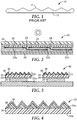
- a prior art monolithic patterned electrical connector 10 comprising a structured major surface 11 and a generally flat opposite major surface 12 has been described, for example, in U.S. Patent Publication No. 2007/0125415 (Sachs ), and is shown in Fig. 1 .
- the structured surface 11 behaves as a light directing medium, reflecting light back to the photovoltaic cell.
- One disadvantage associated with this type of construction relates to the soldering process used to attach the electrical connectors to the photovoltaic cells. When the solder contacts the structured surface 11 of the monolithic electrical connector 10, it destroys at least part of the structure, thereby creating inactive areas.
- a monolithic (i.e., wherein the structured surface is adjacent to and integral with the flat major surface) construction relates to flexibility.
- the flat major surface be flexible and the structured surface be less flexible to provide adequate weathering properties.
- the flat major surface (which is positioned adjacent to the PV cells) have good adhesion to the PV cells, and therefore may be made of a different material than the structured surface.
- the present inventors sought, for example, to develop a PV module that overcomes the above identified deficiencies.
- the present inventors also sought, for example, to develop a PV module that has at least one of increased efficiency, increased energy generation, and increased active area.
- the PV modules of the present application include electrical connectors and light directing mediums which are not damaged by the soldering process.
- the present inventors also sought to develop methods of making these PV modules.
- FIG. 2 is a cross-sectional view of one exemplary embodiment of a PV module according to the present application.
- PV module 20 comprises a plurality of rectangular PV cells 22a, 22b, 22c. Any PV cell can be used in the PV module of the present application.
- Some examples of photovoltaic cells include thin film photovoltaic cells (like Copper Indium Gallium di-Selenide (CIGS)), CIS (CuInSe 2 ) cells, a-Si (amorphous silicon) cells, c-Si (crystalline silicon), and organic photovoltaic devices (OPVs).
- a metallization pattern is applied to the PV cells, most commonly by screen printing of silver inks. This pattern consists of an array of fine parallel gridlines (also known as fingers) (not shown).
- Exemplary PV cells include those made substantially as illustrated and described in U.S. Pat. Nos. 4,751,191 (Gonsiorawski et al ), 5,074,920 (Gonsiorawski et al ), 5,118,362 (St. Angelo et al ), 5,320,684 (Amick et al ) and 5,478,402 (Hanoka ).
- Electrical connectors 24 are disposed over and typically soldered to the PV cells, to collect current from the fingers.
- electrical connectors 24 are provided in the form of coated ( e.g., tinned) copper wires.
- each PV cell includes a rear contact on its rear surface.
- light directing mediums 23 reflect incident sunlight back onto one or more active areas of the PV cells.
- light redirecting medium 23 is positioned adjacent to one or more electrical connectors 24 or portions of electrical connectors 24.
- the light redirecting mediums can be adjacent to the electrical connectors on one or more photovoltaic cells or can be adjacent to the area free of photovoltaic cells as well as to one or more photovoltaic cells.
- Exemplary suitable light directing mediums include, for example, those made of a thermoplastic film having a plurality of parallel grooves coated with a light reflecting coating.
- light directing mediums 23 are bonded to electrical connectors 24. In some embodiments, they are bonded by means of an adhesive 25.
- the adhesive is a thermally-activated (e.g., hot melt adhesive).
- the adhesive is a pressure-sensitive adhesive (PSA).
- PSA pressure-sensitive adhesive
- the adhesive is laminated to the light directing mediums prior to adhesion onto electrical connector 24. In some embodiments, the adhesive is applied over electrical connectors 24 prior to application of one or more light directing mediums 23.
- PV module 20 also includes a back protector member, often in the form of backsheet 28.
- backsheet 28 is an electrically insulating material such as glass, a polymeric layer, a polymeric layer reinforced with reinforcing fibers (e.g., glass, ceramic or polymeric fivers), or a wood particle board.
- backsheet 28 includes a type of glass or quartz.
- the glass is thermally tempered.
- Some exemplary glass materials include soda-lime-silica based glass.
- backsheet 28 is a polymeric film.
- Exemplary backsheets include multilayer polymer films.
- backsheet One commercially available example of a backsheet is the 3MTM ScotchshieldTM film commercially available from 3M Company, Saint Paul, Minnesota. Exemplary backsheets are those that include extruded PTFE.
- the backsheet may be connected to a building material, such as a roofing membrane (for example, in building integrated photovoltaics (BIPV)).
- BIPV building integrated photovoltaics
- front-side layer 30 includes a type of glass or quartz.
- the glass is thermally tempered.
- Some exemplary glass materials include soda-lime-silica based glass.
- the front-side layer has a low iron content (e.g., less than about 0.10% total iron, more preferably less than about 0.08, 0.07 or 0.06% total iron) and/or an antireflection coating thereon to optimize light transmission.
- the front-side layer is a barrier layer.
- Some exemplary barrier layers are those described in, for example, U.S. Patent Nos. 7,186,465 (Bright ), 7,276,291 (Bright ), 5,725,909 (Shaw et al ), 6,231,939 (Shaw et al ), 6,975,067 (McCormick et al ), 6,203,898 (Kohler et al ), 6,348,237 (Kohler et al ), 7,018,713 (Padiyath et al ), and U.S. Publication Nos. 2007/0020451 and 2004/0241454 .
- an encapsulant 32 interposed between backsheet 28, a front-side layer 30, surrounding cells 22a, 22b, 22c, and electrical connectors 24, is an encapsulant 32 which is made of suitable light-transparent, electrically non-conducting material.
- encapsulant 32 is an ethylene vinyl acetate copolymer (EVA), or an ionomer.
- EVA ethylene vinyl acetate copolymer
- the encapsulant 32 is provided in the form of discrete sheets that are positioned below and/or on top of the array of PV cells 22a, 22b, 22c, with those components in turn being sandwiched between the backsheet 28 and the front-side layer 30.
- the laminate construction is heated under vacuum, causing the encapsulant sheets to become liquified enough to flow around and encapsulate the PV cells, while simultaneously filling any voids in the space between the front-side layer and backsheet.
- the liquified encapsulant solidifies.
- the encapsulant may be additionally cured in situ to form a transparent solid matrix. The encapsulant adheres to the front-side layer 30 and backsheet 28 to form a laminated subassembly.
- any encapsulant can be used in methods and constructions of the present disclosure.
- Some exemplary encapsulant types include curable thermosets, thermosettable fluoropolymers, and acrylics.
- Some exemplary encapsulants include ethylene vinyl acetate (EVA), polyvinyl butyral (PVB), polyolefins, thermoplastic urethanes, clear polyvinylchloride, and ionomers.
- EVA ethylene vinyl acetate
- PVB polyvinyl butyral
- polyolefins polyolefins
- thermoplastic urethanes thermoplastic urethanes
- clear polyvinylchloride clear polyvinylchloride
- ionomers ethylene vinyl acetate
- One exemplary commercially available polyolefin encapsulant is PO8500TM, sold by 3M Company. Both thermoplastic and thermoset polyolefin encapsulants can be used.
- a first PV cell 22a is electrically connected to a second cell 22b by electrical connector 24.
- the first and second cells are directly adjacent to one another, but cells that are not directly adjacent fall within the scope of the present application.
- electrical connector 24 extends across the entire length of and over the first cell 22a, extending beyond the edge of the first cell 22a and bending down and under the second cell 22b. Electrical connector 24 then extends across the entire length of and underneath second cell 22b.
- Light directing medium 23 is positioned adjacent to the electrical connector 24.
- light directing medium 23 is provided in the form of a continuous strip of flexible polymeric film, which is placed over the entire length of the PV module 20. In another embodiment, light directing medium is provided with cell length size.
- FIG. 3 is a cross-sectional view of an exemplary embodiment of a PV module 50 according to the present application.
- PV module 50 includes multiple electrical connectors 24.
- electrical connectors 24 are disposed over the entire length of the PV cell.
- Light directing medium 23 is disposed over one or more electrical connectors 24.
- light directing medium 23 completely overlaps with electrical connector 24 in order to maximize efficiency of the PV module.
- light directing medium 23 does not completely overlap electrical connector 24.
- light directing mediums are provided in the form of continuous strips which are slightly wider than the electrical connectors.
- the width of each electrical connector is about 1.5 mm and the width of each light directing medium is about 1.5 mm. In some embodiments, the width of the light directing medium ranges from about 1.5 mm to about 3.0 mm.
- Light directing medium 23 comprises a flexible polymeric layer 34 having a first generally flat major surface 35a and a second generally flat major surface 35b. Structured surface 36 is adjacent to the first major surface 35a of the flexible polymeric layer 34.
- the flexible polymeric layer 34 is one of a polyolefin (e.g., polyethylene, polypropylene), polyester ( e.g., polyethylene terephthalate (PET)), and polyacrylate (e.g., polymethyl(meth)acrylate (PMMA)).
- the structured surface 36 is made of one of a thermoplastic polymer and a polymerizable resin.
- the structured surface further comprises a reflective coating 38, such as, a metalized layer (e.g., aluminum, silver).
- the optimal width of light directing film can be determined based on, for example, at least one of the following factors: the facet design, the index match between the glass and encapsulant, and the thickness of the frontside glass or frontside material.
- the light directing medium has a width of between 5mm and about 30 mm. In some embodiments, the light directing medium has a width of between about 10mm and about 25 mm. In some embodiments, the light directing medium has a width of between about 12 mm and about 20mm. In some embodiments, the light directing medium has a width between about 13 mm and about 18 mm.
- Polymerizable resins suitable for forming structured surfaces include blends of photoinitiator and at least one compound bearing an acrylate group.
- the resin blend contains a monofunctional, a difunctional, or a polyfunctional compound to ensure formation of a cross-linked polymeric network upon irradiation.
- Illustrative examples of resins that are capable of being polymerized by a free radical mechanism that can be used herein include acrylic-based resins derived from epoxies, polyesters, polyethers, and urethanes, ethylenically unsaturated compounds, isocyanate derivatives having at least one pendant acrylate group, epoxy resins other than acrylated epoxies, and mixtures and combinations thereof.
- acrylate is used herein to encompass both acrylates and methacrylates.
- U.S. Pat. 4,576,850 (Martens ) discloses examples of crosslinked resins that may be used in forming the structured surface of light directing medium 23.
- the resin is a non-halogenated resin. Some benefits of use of non-halogenated resins include the fact that they are more environmentally friendly and do not corrode metals.
- the reflective coating is a mirror coating.
- a reflective coating or a mirror coating have several advantages. For example, these coatings can provide reflectivity of incident sunlight and thus can block incident sunlight from being incident on the polymer materials (which can degrade due to UV exposure). Any desired reflective coating or mirror coating thickness can be used. Some exemplary thicknesses are measured by optical density or percent transmission. Obviously, thicker coatings block more UV light. However, coatings that are too thick may cause increased stress within the coating, resulting in coating cracking. Additionally, thicker coatings are often less durable when exposed to damp heat testing and/or pressure cooker testing. Some light directing mediums have a reflective or mirror coating thickness of between about 35 nm to about 60 nm.
- One exemplary method of making PV modules as described herein includes the steps of: providing strings of photovoltaic cells, soldering electrical connectors over the photovoltaic cells, and adhering light directing mediums over the electrical connectors.
- the light directing mediums are previously laminated with an adhesive.
- the adhesive is a hot-melt adhesive.
- the hot-melt adhesive is ethylene vinyl acetate polymer (EVA).
- EVA ethylene vinyl acetate polymer
- Other types of suitable hot-melt adhesives include polyolefins.
- other layers may be laminated or coated onto the PV module (e.g., backsheets, encapsulants, front-side layers) prior to the heating step.
- the heating step may be carried out using any suitable heating mechanism such as, for example, a heat gun or infrared heater.
- the heating mechanism is placed under the laminate construction ( e.g., adjacent to the backsheet).
- the heating mechanism is placed above the laminate construction ( e.g., adjacent to the light directing medium).
- the adhesive is a pressure-sensitive adhesive (PSA).
- PSA pressure-sensitive adhesive
- Suitable types of PSAs include, but are not limited to, acrylates, silicones, polyisobutylenes, ureas, and combinations thereof.
- the PSA is an acrylic or acrylate PSA.
- the term "acrylic” or “acrylate” includes compounds having at least one of acrylic or methacrylic groups.
- Useful acrylic PSAs can be made, for example, by combining at least two different monomers (first and second monomers).
- Exemplary suitable first monomers include 2-methylbutyl acrylate, 2-ethylhexyl acrylate, isooctyl acrylate, lauryl acrylate, n-decyl acrylate, 4-methyl-2-pentyl acrylate, isoamyl acrylate, sec-butyl acrylate, and isononyl acrylate.
- Exemplary suitable second monomers include a (meth)acrylic acid (e.g., acrylic acid, methacrylic acid, itaconic acid, maleic acid, and fumaric acid), a (meth)acrylamide (e.g., acrylamide, methacrylamide, N-ethyl acrylamide, N-hydroxyethyl acrylamide, N-octyl acrylamide, N-t-butyl acrylamide, N,N-dimethyl acrylamide, N,Ndiethyl acrylamide, and N-ethyl-N-dihydroxyethyl acrylamide), a (meth)acrylate (e.g., 2- hydroxyethyl acrylate or methacrylate, cyclohexyl acrylate, t-butyl acrylate, or isobornyl acrylate), N-vinyl pyrrolidone, N-vinyl caprolactam, an alpha-olefin, a vinyl ether,
- the adhesive is selectively applied to the electrical connectors, with the width of the light directing mediums being slightly larger than the width of the electrical connectors.
- the adhesive is transparent. Desired transparency is at least 80% transparency to visible light. In some embodiments, the desired transparency is at least 90% to visible light.
- the transparent adhesive is applied over the entire surface of the PV cells ( e.g., flood coated). The light directing mediums are then carefully positioned over, and in registration with, the electrical connectors. The entire structure is then heated to melt the adhesive and ensure adequate bonding of the light directing mediums to the electrical connectors.
- the words “on” and “adjacent” cover both a layer being directly on and indirectly on something, with other layers possibly being located therebetween.
- major surface and “major surfaces” refer to the surface(s) with the largest surface area on a three-dimensional shape having three sets of opposing surfaces.
Landscapes
- Engineering & Computer Science (AREA)
- Microelectronics & Electronic Packaging (AREA)
- Electromagnetism (AREA)
- General Physics & Mathematics (AREA)
- Condensed Matter Physics & Semiconductors (AREA)
- Computer Hardware Design (AREA)
- Physics & Mathematics (AREA)
- Power Engineering (AREA)
- Life Sciences & Earth Sciences (AREA)
- Sustainable Development (AREA)
- Photovoltaic Devices (AREA)
- Manufacturing & Machinery (AREA)
- Sustainable Energy (AREA)
Claims (6)
- Module photovoltaïque (20, 50), comprenant :une pluralité de cellules photovoltaïques (22a, 22b, 22c) incluant une première cellule photovoltaïque et une deuxième cellule photovoltaïque espacées l'une de l'autre pour former une zone qui est exempte de cellules photovoltaïques ;un connecteur électrique (24) connectant au moins les première et deuxième cellules photovoltaïques ;un milieu d'orientation de lumière (23) positionné sur le connecteur électrique (24) sur au moins une partie de la première cellule photovoltaïque ; etun adhésif (25) entre le connecteur électrique (24) et le milieu d'orientation de lumière (23) ;dans lequel l'adhésif (25) lie le milieu d'orientation de lumière (23) au connecteur électrique (24) ;caractérisé en ce que le milieu d'orientation de lumière (23) est une construction multicouche comprenant, dans l'ordre cité :une couche polymère souple généralement plane (34), adjacente à l'adhésif,une couche structurée (36), etun revêtement réfléchissant (38),dans lequel le milieu d'orientation de lumière (23) et le connecteur électrique (24) ont une longueur et une largeur dans le plan de la construction multicouche, et dans lequel la largeur du milieu d'orientation de lumière (23) est plus grande que la largeur du connecteur électrique (24).
- Module photovoltaïque selon la revendication 1, dans lequel le milieu d'orientation de lumière (23) est positionné sur l'au moins une partie de la première cellule photovoltaïque et sur au moins une partie de la deuxième cellule photovoltaïque et s'étend à travers au moins une partie de la zone qui est exempte de cellules photovoltaïques.
- Module photovoltaïque selon la revendication 1 ou la revendication 2, dans lequel la couche structurée (36) comprend une résine non halogénée.
- Procédé de fabrication d'un module photovoltaïque (20, 50) incluant une pluralité de cellules photovoltaïques (22a, 22b, 22c) incluant une première cellule photovoltaïque et une deuxième cellule photovoltaïque qui sont espacées l'une de l'autre pour former une zone exempte de cellules photovoltaïques, comprenant :la connexion électrique de la première cellule photovoltaïque et de la deuxième cellule photovoltaïque avec un connecteur électrique (24) ;le positionnement d'un milieu d'orientation de lumière sur le connecteur électrique (24) adjacent à au moins une partie de la première cellule photovoltaïque ; etle positionnement d'un adhésif (25) entre le connecteur électrique (24) et le milieu d'orientation de lumière (23),dans lequel l'adhésif lie le milieu d'orientation de lumière (23) au connecteur électrique (24) ;caractérisé en ce que le milieu d'orientation de lumière (23) est une construction multicouche comprenant, dans l'ordre cité :une couche polymère souple généralement plane (34), adjacente à l'adhésif (25),une couche structurée (36), etun revêtement réfléchissant (38),dans lequel le milieu d'orientation de lumière (23) et le connecteur électrique (24) ont une longueur et une largeur dans le plan de la construction multicouche, et dans lequel la largeur du milieu d'orientation de lumière (23) est plus grande que la largeur du connecteur électrique (24).
- Procédé selon la revendication 4, comprenant en outre :
le positionnement du milieu d'orientation de lumière (23) adjacent à la deuxième cellule photovoltaïque et s'étendant à travers au moins une partie de la zone exempte de cellules photovoltaïques. - Procédé selon l'une quelconque des revendications 4 ou 5, comprenant en outre l'étape consistant à :
chauffer le module photovoltaïque (20, 50) pour fondre l'adhésif (25) et faire adhérer efficacement le milieu d'orientation de lumière (23) au connecteur électrique (24).
Applications Claiming Priority (2)
| Application Number | Priority Date | Filing Date | Title |
|---|---|---|---|
| US201261616205P | 2012-03-27 | 2012-03-27 | |
| PCT/US2013/030367 WO2013148149A1 (fr) | 2012-03-27 | 2013-03-12 | Modules photovoltaïques comportant des milieux orientant la lumière et procédés pour leur fabrication |
Publications (3)
| Publication Number | Publication Date |
|---|---|
| EP2831922A1 EP2831922A1 (fr) | 2015-02-04 |
| EP2831922A4 EP2831922A4 (fr) | 2015-12-09 |
| EP2831922B1 true EP2831922B1 (fr) | 2020-07-22 |
Family
ID=49261008
Family Applications (1)
| Application Number | Title | Priority Date | Filing Date |
|---|---|---|---|
| EP13769124.2A Active EP2831922B1 (fr) | 2012-03-27 | 2013-03-12 | Modules photovoltaïques comportant des milieux orientant la lumière et procédés pour leur fabrication |
Country Status (7)
| Country | Link |
|---|---|
| US (1) | US9972734B2 (fr) |
| EP (1) | EP2831922B1 (fr) |
| JP (2) | JP6510401B2 (fr) |
| KR (1) | KR101985053B1 (fr) |
| CN (2) | CN110246918A (fr) |
| ES (1) | ES2824125T3 (fr) |
| WO (1) | WO2013148149A1 (fr) |
Families Citing this family (18)
| Publication number | Priority date | Publication date | Assignee | Title |
|---|---|---|---|---|
| CN110246918A (zh) | 2012-03-27 | 2019-09-17 | 3M创新有限公司 | 包括光定向介质的光伏组件及其制备方法 |
| US9502596B2 (en) * | 2013-06-28 | 2016-11-22 | Sunpower Corporation | Patterned thin foil |
| DE112015004480T5 (de) * | 2014-09-30 | 2017-06-22 | Panasonic Intellectual Property Management Co., Ltd. | Solarbatteriemodul |
| JP6671029B2 (ja) * | 2015-03-03 | 2020-03-25 | パナソニックIpマネジメント株式会社 | 太陽電池モジュール |
| WO2016168164A1 (fr) * | 2015-04-17 | 2016-10-20 | 3M Innovative Properties Company | Film de redirection de lumière utile avec des modules solaires |
| RU2657114C1 (ru) | 2015-07-21 | 2018-06-08 | Конинклейке Филипс Н.В. | Слоистое изделие с преобразователем |
| WO2017066146A1 (fr) * | 2015-10-12 | 2017-04-20 | 3M Innovative Properties Company | Film de redirection de lumière utile avec des modules solaires |
| JP2019526653A (ja) * | 2016-07-07 | 2019-09-19 | スリーエム イノベイティブ プロパティズ カンパニー | 光方向転換フィルム用接着剤 |
| EP3494602A4 (fr) * | 2016-08-02 | 2020-03-04 | 3M Innovative Properties Company | Systèmes et procédés de fabrication comprenant une découpe en ligne |
| US20190326462A1 (en) * | 2016-12-22 | 2019-10-24 | Suzhou Golden Star Electronic Technology Co., Ltd | Photovoltaic reflective film and application thereof |
| CN207474483U (zh) * | 2017-12-12 | 2018-06-08 | 米亚索乐装备集成(福建)有限公司 | 柔性光伏组件 |
| WO2019150237A1 (fr) * | 2018-01-30 | 2019-08-08 | 3M Innovative Properties Company | Films de redirection de lumière et son procédé de fabrication et modules photovoltaïques |
| CN110120430A (zh) * | 2018-01-30 | 2019-08-13 | 法国圣戈班玻璃厂 | 带有具有改进雾度的局部结构的盖板玻璃的光伏组件及其制备方法 |
| CN108877981A (zh) * | 2018-06-22 | 2018-11-23 | 中国工程物理研究院核物理与化学研究所 | 一种氚荧光同位素电池 |
| WO2020044240A1 (fr) | 2018-08-31 | 2020-03-05 | 3M Innovative Properties Company | Film de redirection de lumière ayant des propriétés d'atténuation de la lumière parasite utiles avec des modules solaires |
| US20200127152A1 (en) | 2018-09-14 | 2020-04-23 | 3M Innovative Properties Company | Bifacial solar panel |
| WO2021124034A1 (fr) * | 2019-12-16 | 2021-06-24 | 3M Innovative Properties Company | Film de redirection de lumière ayant une durabilité améliorée utile avec des modules solaires |
| EP4078688A4 (fr) * | 2019-12-19 | 2024-01-17 | 3M Innovative Properties Company | Film de redirection de lumière |
Family Cites Families (88)
| Publication number | Priority date | Publication date | Assignee | Title |
|---|---|---|---|---|
| US4235643A (en) | 1978-06-30 | 1980-11-25 | Exxon Research & Engineering Co. | Solar cell module |
| US4576850A (en) | 1978-07-20 | 1986-03-18 | Minnesota Mining And Manufacturing Company | Shaped plastic articles having replicated microstructure surfaces |
| US4307150A (en) | 1979-08-13 | 1981-12-22 | Minnesota Mining And Manufacturing Company | Weatherable solar reflector |
| US4246042A (en) | 1980-02-13 | 1981-01-20 | Science Applications, Inc. | Fixed solar energy concentrator |
| US4751191A (en) | 1987-07-08 | 1988-06-14 | Mobil Solar Energy Corporation | Method of fabricating solar cells with silicon nitride coating |
| US5122902A (en) | 1989-03-31 | 1992-06-16 | Minnesota Mining And Manufacturing Company | Retroreflective articles having light-transmissive surfaces |
| US5076857A (en) | 1990-08-27 | 1991-12-31 | Spire Corporation | Photovoltaic cell and process |
| US5118362A (en) | 1990-09-24 | 1992-06-02 | Mobil Solar Energy Corporation | Electrical contacts and methods of manufacturing same |
| US5074920A (en) | 1990-09-24 | 1991-12-24 | Mobil Solar Energy Corporation | Photovoltaic cells with improved thermal stability |
| US5178685A (en) | 1991-06-11 | 1993-01-12 | Mobil Solar Energy Corporation | Method for forming solar cell contacts and interconnecting solar cells |
| US5328696A (en) | 1991-07-22 | 1994-07-12 | Dow Corning Corporation | Devices using silicone pressure sensitive adhesives containing organic wax |
| US5320684A (en) | 1992-05-27 | 1994-06-14 | Mobil Solar Energy Corporation | Solar cell and method of making same |
| WO1994004111A1 (fr) | 1992-08-21 | 1994-03-03 | The Procter & Gamble Company | Systemes de fermeture adhesifs refermables pour articles absorbants jetables en conditionnement individuel |
| ATE233939T1 (de) | 1993-10-04 | 2003-03-15 | 3M Innovative Properties Co | Vernetztes acrylatbeschichtungsmaterial zur herstellung von kondensatordielektrika und sauerstoffbarrieren |
| US20040241454A1 (en) | 1993-10-04 | 2004-12-02 | Shaw David G. | Barrier sheet and method of making same |
| US5478402A (en) | 1994-02-17 | 1995-12-26 | Ase Americas, Inc. | Solar cell modules and method of making same |
| US5554229A (en) | 1995-02-21 | 1996-09-10 | United Solar Systems Corporation | Light directing element for photovoltaic device and method of manufacture |
| US6280063B1 (en) | 1997-05-09 | 2001-08-28 | 3M Innovative Properties Company | Brightness enhancement article |
| US6203898B1 (en) | 1997-08-29 | 2001-03-20 | 3M Innovatave Properties Company | Article comprising a substrate having a silicone coating |
| JP3670835B2 (ja) | 1998-04-22 | 2005-07-13 | 三洋電機株式会社 | 太陽電池モジュール |
| US5994641A (en) * | 1998-04-24 | 1999-11-30 | Ase Americas, Inc. | Solar module having reflector between cells |
| WO2000026973A1 (fr) | 1998-11-02 | 2000-05-11 | Presstek, Inc. | Oxydes conducteurs transparents pour ecran plat en plastique |
| US6440334B2 (en) * | 1999-06-11 | 2002-08-27 | 3M Innovative Properties Company | Method of making a retroreflective article |
| US7022910B2 (en) | 2002-03-29 | 2006-04-04 | Konarka Technologies, Inc. | Photovoltaic cells utilizing mesh electrodes |
| US6657009B2 (en) | 2000-12-29 | 2003-12-02 | Kimberly-Clark Worldwide, Inc. | Hot-melt adhesive having improved bonding strength |
| US6758992B2 (en) | 2001-02-28 | 2004-07-06 | 3M Innovative Properties Company | Process of stripe coating to produce microstructured composite articles |
| US20030035231A1 (en) | 2001-08-03 | 2003-02-20 | Epstein Kenneth A. | Optical film having microreplicated structures; and methods |
| US6660930B1 (en) | 2002-06-12 | 2003-12-09 | Rwe Schott Solar, Inc. | Solar cell modules with improved backskin |
| US6975067B2 (en) | 2002-12-19 | 2005-12-13 | 3M Innovative Properties Company | Organic electroluminescent device and encapsulation method |
| US7018713B2 (en) | 2003-04-02 | 2006-03-28 | 3M Innovative Properties Company | Flexible high-temperature ultrabarrier |
| US20080000517A1 (en) | 2003-06-10 | 2008-01-03 | Gonsiorawski Ronald C | Photovoltaic module with light reflecting backskin |
| JP4570373B2 (ja) | 2004-02-26 | 2010-10-27 | 京セラ株式会社 | 太陽電池モジュール |
| JP4404753B2 (ja) | 2004-11-24 | 2010-01-27 | 三洋電機株式会社 | 太陽電池モジュール |
| US20070020451A1 (en) | 2005-07-20 | 2007-01-25 | 3M Innovative Properties Company | Moisture barrier coatings |
| US7467873B2 (en) | 2005-10-14 | 2008-12-23 | 3M Innovative Properties Company | Privacy film |
| US20070125415A1 (en) | 2005-12-05 | 2007-06-07 | Massachusetts Institute Of Technology | Light capture with patterned solar cell bus wires |
| US20070147712A1 (en) | 2005-12-19 | 2007-06-28 | 3M Innovative Properties Company | Method of making articles for storing and organizing materials |
| US20070138044A1 (en) | 2005-12-19 | 2007-06-21 | Trotter Byron E | Article for storing and organizing materials |
| US8581094B2 (en) | 2006-09-20 | 2013-11-12 | Dow Global Technologies, Llc | Electronic device module comprising polyolefin copolymer |
| JP5091490B2 (ja) | 2007-01-22 | 2012-12-05 | 富士フイルム株式会社 | 光学シート及びその製造方法 |
| JP2008311604A (ja) * | 2007-02-06 | 2008-12-25 | Hitachi Chem Co Ltd | 太陽電池モジュール及び太陽電池モジュール用波長変換型集光フィルム |
| CN101647124B (zh) * | 2007-02-06 | 2011-09-14 | 美国太阳能科技公司 | 太阳能电模块 |
| WO2008097507A1 (fr) * | 2007-02-06 | 2008-08-14 | American Solar Technologies, Inc. | Module solaire à réorientation de lumière incidente |
| US20080291541A1 (en) | 2007-05-23 | 2008-11-27 | 3M Innovative Properties Company | Light redirecting solar control film |
| GB2449504A (en) | 2007-05-25 | 2008-11-26 | Renewable Energy Corp Asa | Photovoltaic module with reflective V-grooves |
| US20090041553A1 (en) | 2007-08-06 | 2009-02-12 | 3M Innovative Properties Company | Fly-cutting system and method, and related tooling and articles |
| US9180524B2 (en) | 2007-08-06 | 2015-11-10 | 3M Innovative Properties Company | Fly-cutting head, system and method, and tooling and sheeting produced therewith |
| JP5195764B2 (ja) | 2007-12-10 | 2013-05-15 | トヨタ自動車株式会社 | 太陽電池モジュール |
| JP2009206494A (ja) * | 2008-01-31 | 2009-09-10 | Sanyo Electric Co Ltd | 太陽電池モジュール |
| KR20110000695A (ko) * | 2008-04-11 | 2011-01-04 | 퀄컴 엠이엠스 테크놀로지스, 인크. | Pv 심미성 및 효율의 향상방법 |
| US20090314329A1 (en) | 2008-06-24 | 2009-12-24 | Moser Baer Photovoltaic Limited | Photovoltaic module |
| US20090320908A1 (en) * | 2008-06-27 | 2009-12-31 | Sunpower Corp. | Photovoltaic module with drainage frame |
| JP5436805B2 (ja) | 2008-07-04 | 2014-03-05 | 三洋電機株式会社 | 太陽電池モジュール |
| JP2012503221A (ja) | 2008-09-18 | 2012-02-02 | クォルコム・メムズ・テクノロジーズ・インコーポレーテッド | 太陽光収集器/集光器における光収集の角度範囲の増大化 |
| JP2010087060A (ja) | 2008-09-30 | 2010-04-15 | Sanyo Electric Co Ltd | 太陽電池モジュール |
| CN102232246B (zh) | 2008-10-03 | 2014-02-26 | 凸版印刷株式会社 | 太阳能电池模块 |
| US20110240095A1 (en) | 2008-11-19 | 2011-10-06 | Toppan Printing Co., Ltd. | Light reuse sheet, solar battery module, and light source module |
| CN102217089B (zh) | 2008-11-19 | 2014-12-17 | 凸版印刷株式会社 | 光再利用片和太阳能电池模块 |
| JP4706759B2 (ja) | 2009-01-23 | 2011-06-22 | トヨタ自動車株式会社 | 太陽電池 |
| US20100186570A1 (en) | 2009-01-29 | 2010-07-29 | 3M Innovative Properties Company | Method for making an optical film having a variable prismatic structured surface |
| JP2010147454A (ja) | 2009-04-03 | 2010-07-01 | Toppan Printing Co Ltd | 太陽電池モジュール用光再利用シート及び太陽電池モジュール |
| WO2010135801A1 (fr) | 2009-05-25 | 2010-12-02 | Day4 Energy Lnc. | Agencement de chaînes de modules photovoltaïques et protection contre l'ombre |
| KR100990114B1 (ko) | 2009-07-07 | 2010-10-29 | 엘지전자 주식회사 | 인터커넥터를 구비한 태양 전지 모듈 및 이의 제조 방법 |
| AT11607U1 (de) * | 2009-08-25 | 2011-01-15 | Zumtobel Lighting Gmbh | Lichtemittierende vorrichtung |
| JP2011108725A (ja) | 2009-11-13 | 2011-06-02 | Toppan Printing Co Ltd | 裏面シート、太陽電池裏面シート及びこれを用いた太陽電池モジュール |
| KR20110064969A (ko) * | 2009-12-09 | 2011-06-15 | 엘지전자 주식회사 | 태양 전지 모듈 |
| CN102656488A (zh) | 2009-12-17 | 2012-09-05 | 3M创新有限公司 | 光重新定向构造 |
| KR101614166B1 (ko) * | 2010-04-29 | 2016-04-20 | 엘지전자 주식회사 | 태양 전지 모듈 및 그 제조 방법 |
| DE102010016771B4 (de) * | 2010-05-04 | 2017-08-24 | Solarworld Innovations Gmbh | Verfahren zum Fixieren eines Photovoltaik-Zellenverbinders auf einer Oberfläche einer Photovoltaik-Zelle |
| JP5842166B2 (ja) | 2010-06-25 | 2016-01-13 | パナソニックIpマネジメント株式会社 | 太陽電池モジュールおよび太陽電池モジュールの製造方法 |
| CN102347375A (zh) | 2010-07-30 | 2012-02-08 | E·I·内穆尔杜邦公司 | 一种包括覆盖着反射条的导电带的太阳能电池模块 |
| EP2646858A2 (fr) | 2010-12-01 | 2013-10-09 | 3M Innovative Properties Company | Articles microstructurés comportant des nanostructures et procédé |
| US20130251945A1 (en) | 2010-12-14 | 2013-09-26 | 3M Innovative Properties Company | Images and method of making the same |
| KR20140054065A (ko) | 2011-07-19 | 2014-05-08 | 쓰리엠 이노베이티브 프로퍼티즈 컴파니 | 양면형 일광 방향 변경 필름 |
| JP5672553B2 (ja) | 2011-08-24 | 2015-02-18 | パナソニックIpマネジメント株式会社 | 機器の取付構造 |
| US9004726B2 (en) | 2011-10-27 | 2015-04-14 | Svv Technology Innovations, Inc. | Light directing films |
| US9379263B2 (en) | 2011-11-04 | 2016-06-28 | 3M Innovative Properties Company | Durable polyolefin adhesive material for solar modules |
| JP2015503219A (ja) | 2011-11-04 | 2015-01-29 | スリーエム イノベイティブ プロパティズ カンパニー | ソーラーモジュールにおける使用のためのポリオレフィン接着剤 |
| JP5971927B2 (ja) | 2011-11-29 | 2016-08-17 | デクセリアルズ株式会社 | 光学体、窓材、建具、日射遮蔽装置および建築物 |
| CN110246918A (zh) | 2012-03-27 | 2019-09-17 | 3M创新有限公司 | 包括光定向介质的光伏组件及其制备方法 |
| US9812590B2 (en) | 2012-10-25 | 2017-11-07 | Sunpower Corporation | Bifacial solar cell module with backside reflector |
| US9714756B2 (en) | 2013-03-15 | 2017-07-25 | Morgan Solar Inc. | Illumination device |
| CN105378946A (zh) | 2013-07-09 | 2016-03-02 | 3M创新有限公司 | 用于太阳能组件的带有含曲面微结构的反射微结构化膜 |
| US20160172517A1 (en) | 2013-07-09 | 2016-06-16 | 3M Innovative Properties Company | Reflecting films with rounded microstructures for use in solar modules |
| US9850405B2 (en) | 2013-10-02 | 2017-12-26 | 3M Innovative Properties Company | Article comprising polyacrylate pressure sensitive primer and adhesive comprising polyacrylate component |
| EP3084487B1 (fr) | 2013-12-19 | 2024-03-20 | Bright View Technologies Corporation | Diffuseurs anti-éblouissement 2d à augmentation d'intensité lumineuse axiale |
| WO2016168164A1 (fr) | 2015-04-17 | 2016-10-20 | 3M Innovative Properties Company | Film de redirection de lumière utile avec des modules solaires |
| WO2017066146A1 (fr) | 2015-10-12 | 2017-04-20 | 3M Innovative Properties Company | Film de redirection de lumière utile avec des modules solaires |
-
2013
- 2013-03-12 CN CN201910449973.6A patent/CN110246918A/zh not_active Withdrawn
- 2013-03-12 US US14/387,613 patent/US9972734B2/en active Active
- 2013-03-12 CN CN201380016857.6A patent/CN104471722A/zh active Pending
- 2013-03-12 JP JP2015503251A patent/JP6510401B2/ja active Active
- 2013-03-12 KR KR1020147029573A patent/KR101985053B1/ko active IP Right Grant
- 2013-03-12 ES ES13769124T patent/ES2824125T3/es active Active
- 2013-03-12 WO PCT/US2013/030367 patent/WO2013148149A1/fr active Application Filing
- 2013-03-12 EP EP13769124.2A patent/EP2831922B1/fr active Active
-
2018
- 2018-12-06 JP JP2018229282A patent/JP6686116B2/ja active Active
Non-Patent Citations (1)
| Title |
|---|
| None * |
Also Published As
| Publication number | Publication date |
|---|---|
| KR101985053B1 (ko) | 2019-05-31 |
| ES2824125T3 (es) | 2021-05-11 |
| US9972734B2 (en) | 2018-05-15 |
| EP2831922A1 (fr) | 2015-02-04 |
| CN110246918A (zh) | 2019-09-17 |
| JP6686116B2 (ja) | 2020-04-22 |
| US20150155411A1 (en) | 2015-06-04 |
| EP2831922A4 (fr) | 2015-12-09 |
| JP2015515753A (ja) | 2015-05-28 |
| WO2013148149A1 (fr) | 2013-10-03 |
| JP2019050422A (ja) | 2019-03-28 |
| CN104471722A (zh) | 2015-03-25 |
| KR20140146620A (ko) | 2014-12-26 |
| JP6510401B2 (ja) | 2019-05-08 |
Similar Documents
| Publication | Publication Date | Title |
|---|---|---|
| EP2831922B1 (fr) | Modules photovoltaïques comportant des milieux orientant la lumière et procédés pour leur fabrication | |
| US10903382B2 (en) | Light redirecting film useful with solar modules | |
| CN107845697B (zh) | 用于光重定向膜的粘合剂 | |
| KR101215694B1 (ko) | 태양 전지 모듈 및 태양 전지 모듈의 제조 방법 | |
| US20180040757A1 (en) | Light redirecting film useful with solar modules | |
| US20110139225A1 (en) | Shaped photovoltaic module | |
| US20120133012A1 (en) | Composite system for photovoltaic modules | |
| CN102623553A (zh) | 一种太阳能电池组件的制备方法 | |
| CN116247120A (zh) | 光伏电池组件的制造方法及光伏电池组件 | |
| AU2018101273A4 (en) | Photovoltaic Building Material Sealed with a Solar Module | |
| US10950745B2 (en) | Manufacturing systems and methods including inline cutting | |
| US20090308447A1 (en) | Photovoltaic module with at least one crystalline solar cell | |
| US20230178680A1 (en) | Photovoltaic cell module and manufacturing method thereof | |
| WO2013134784A1 (fr) | Couche déviatrice de lumière pour panneaux solaires photovoltaïques | |
| CN215184006U (zh) | 一种半柔性太阳能光伏组件 | |
| JPH11284216A (ja) | 光起電力素子、太陽電池モジュ―ル、その製造方法、施工方法及び太陽光発電システム | |
| CN116914034A (zh) | 光伏组件及其制备方法 |
Legal Events
| Date | Code | Title | Description |
|---|---|---|---|
| PUAI | Public reference made under article 153(3) epc to a published international application that has entered the european phase |
Free format text: ORIGINAL CODE: 0009012 |
|
| 17P | Request for examination filed |
Effective date: 20141002 |
|
| AK | Designated contracting states |
Kind code of ref document: A1 Designated state(s): AL AT BE BG CH CY CZ DE DK EE ES FI FR GB GR HR HU IE IS IT LI LT LU LV MC MK MT NL NO PL PT RO RS SE SI SK SM TR |
|
| AX | Request for extension of the european patent |
Extension state: BA ME |
|
| DAX | Request for extension of the european patent (deleted) | ||
| RA4 | Supplementary search report drawn up and despatched (corrected) |
Effective date: 20151110 |
|
| RIC1 | Information provided on ipc code assigned before grant |
Ipc: H01L 31/05 20140101ALI20151104BHEP Ipc: H01L 31/054 20140101ALI20151104BHEP Ipc: H01L 31/048 20140101AFI20151104BHEP |
|
| STAA | Information on the status of an ep patent application or granted ep patent |
Free format text: STATUS: EXAMINATION IS IN PROGRESS |
|
| 17Q | First examination report despatched |
Effective date: 20190613 |
|
| GRAP | Despatch of communication of intention to grant a patent |
Free format text: ORIGINAL CODE: EPIDOSNIGR1 |
|
| STAA | Information on the status of an ep patent application or granted ep patent |
Free format text: STATUS: GRANT OF PATENT IS INTENDED |
|
| INTG | Intention to grant announced |
Effective date: 20200203 |
|
| GRAS | Grant fee paid |
Free format text: ORIGINAL CODE: EPIDOSNIGR3 |
|
| GRAA | (expected) grant |
Free format text: ORIGINAL CODE: 0009210 |
|
| STAA | Information on the status of an ep patent application or granted ep patent |
Free format text: STATUS: THE PATENT HAS BEEN GRANTED |
|
| AK | Designated contracting states |
Kind code of ref document: B1 Designated state(s): AL AT BE BG CH CY CZ DE DK EE ES FI FR GB GR HR HU IE IS IT LI LT LU LV MC MK MT NL NO PL PT RO RS SE SI SK SM TR |
|
| REG | Reference to a national code |
Ref country code: GB Ref legal event code: FG4D |
|
| REG | Reference to a national code |
Ref country code: CH Ref legal event code: EP |
|
| REG | Reference to a national code |
Ref country code: DE Ref legal event code: R096 Ref document number: 602013070924 Country of ref document: DE |
|
| REG | Reference to a national code |
Ref country code: AT Ref legal event code: REF Ref document number: 1294223 Country of ref document: AT Kind code of ref document: T Effective date: 20200815 |
|
| REG | Reference to a national code |
Ref country code: IE Ref legal event code: FG4D |
|
| REG | Reference to a national code |
Ref country code: LT Ref legal event code: MG4D |
|
| REG | Reference to a national code |
Ref country code: AT Ref legal event code: MK05 Ref document number: 1294223 Country of ref document: AT Kind code of ref document: T Effective date: 20200722 |
|
| PG25 | Lapsed in a contracting state [announced via postgrant information from national office to epo] |
Ref country code: FI Free format text: LAPSE BECAUSE OF FAILURE TO SUBMIT A TRANSLATION OF THE DESCRIPTION OR TO PAY THE FEE WITHIN THE PRESCRIBED TIME-LIMIT Effective date: 20200722 Ref country code: SE Free format text: LAPSE BECAUSE OF FAILURE TO SUBMIT A TRANSLATION OF THE DESCRIPTION OR TO PAY THE FEE WITHIN THE PRESCRIBED TIME-LIMIT Effective date: 20200722 Ref country code: NO Free format text: LAPSE BECAUSE OF FAILURE TO SUBMIT A TRANSLATION OF THE DESCRIPTION OR TO PAY THE FEE WITHIN THE PRESCRIBED TIME-LIMIT Effective date: 20201022 Ref country code: GR Free format text: LAPSE BECAUSE OF FAILURE TO SUBMIT A TRANSLATION OF THE DESCRIPTION OR TO PAY THE FEE WITHIN THE PRESCRIBED TIME-LIMIT Effective date: 20201023 Ref country code: PT Free format text: LAPSE BECAUSE OF FAILURE TO SUBMIT A TRANSLATION OF THE DESCRIPTION OR TO PAY THE FEE WITHIN THE PRESCRIBED TIME-LIMIT Effective date: 20201123 Ref country code: BG Free format text: LAPSE BECAUSE OF FAILURE TO SUBMIT A TRANSLATION OF THE DESCRIPTION OR TO PAY THE FEE WITHIN THE PRESCRIBED TIME-LIMIT Effective date: 20201022 Ref country code: LT Free format text: LAPSE BECAUSE OF FAILURE TO SUBMIT A TRANSLATION OF THE DESCRIPTION OR TO PAY THE FEE WITHIN THE PRESCRIBED TIME-LIMIT Effective date: 20200722 Ref country code: AT Free format text: LAPSE BECAUSE OF FAILURE TO SUBMIT A TRANSLATION OF THE DESCRIPTION OR TO PAY THE FEE WITHIN THE PRESCRIBED TIME-LIMIT Effective date: 20200722 Ref country code: HR Free format text: LAPSE BECAUSE OF FAILURE TO SUBMIT A TRANSLATION OF THE DESCRIPTION OR TO PAY THE FEE WITHIN THE PRESCRIBED TIME-LIMIT Effective date: 20200722 |
|
| PG25 | Lapsed in a contracting state [announced via postgrant information from national office to epo] |
Ref country code: IS Free format text: LAPSE BECAUSE OF FAILURE TO SUBMIT A TRANSLATION OF THE DESCRIPTION OR TO PAY THE FEE WITHIN THE PRESCRIBED TIME-LIMIT Effective date: 20201122 Ref country code: RS Free format text: LAPSE BECAUSE OF FAILURE TO SUBMIT A TRANSLATION OF THE DESCRIPTION OR TO PAY THE FEE WITHIN THE PRESCRIBED TIME-LIMIT Effective date: 20200722 Ref country code: LV Free format text: LAPSE BECAUSE OF FAILURE TO SUBMIT A TRANSLATION OF THE DESCRIPTION OR TO PAY THE FEE WITHIN THE PRESCRIBED TIME-LIMIT Effective date: 20200722 Ref country code: PL Free format text: LAPSE BECAUSE OF FAILURE TO SUBMIT A TRANSLATION OF THE DESCRIPTION OR TO PAY THE FEE WITHIN THE PRESCRIBED TIME-LIMIT Effective date: 20200722 |
|
| PG25 | Lapsed in a contracting state [announced via postgrant information from national office to epo] |
Ref country code: NL Free format text: LAPSE BECAUSE OF FAILURE TO SUBMIT A TRANSLATION OF THE DESCRIPTION OR TO PAY THE FEE WITHIN THE PRESCRIBED TIME-LIMIT Effective date: 20200722 |
|
| REG | Reference to a national code |
Ref country code: DE Ref legal event code: R097 Ref document number: 602013070924 Country of ref document: DE |
|
| PG25 | Lapsed in a contracting state [announced via postgrant information from national office to epo] |
Ref country code: EE Free format text: LAPSE BECAUSE OF FAILURE TO SUBMIT A TRANSLATION OF THE DESCRIPTION OR TO PAY THE FEE WITHIN THE PRESCRIBED TIME-LIMIT Effective date: 20200722 Ref country code: DK Free format text: LAPSE BECAUSE OF FAILURE TO SUBMIT A TRANSLATION OF THE DESCRIPTION OR TO PAY THE FEE WITHIN THE PRESCRIBED TIME-LIMIT Effective date: 20200722 Ref country code: CZ Free format text: LAPSE BECAUSE OF FAILURE TO SUBMIT A TRANSLATION OF THE DESCRIPTION OR TO PAY THE FEE WITHIN THE PRESCRIBED TIME-LIMIT Effective date: 20200722 Ref country code: IT Free format text: LAPSE BECAUSE OF FAILURE TO SUBMIT A TRANSLATION OF THE DESCRIPTION OR TO PAY THE FEE WITHIN THE PRESCRIBED TIME-LIMIT Effective date: 20200722 Ref country code: SM Free format text: LAPSE BECAUSE OF FAILURE TO SUBMIT A TRANSLATION OF THE DESCRIPTION OR TO PAY THE FEE WITHIN THE PRESCRIBED TIME-LIMIT Effective date: 20200722 Ref country code: RO Free format text: LAPSE BECAUSE OF FAILURE TO SUBMIT A TRANSLATION OF THE DESCRIPTION OR TO PAY THE FEE WITHIN THE PRESCRIBED TIME-LIMIT Effective date: 20200722 |
|
| REG | Reference to a national code |
Ref country code: ES Ref legal event code: FG2A Ref document number: 2824125 Country of ref document: ES Kind code of ref document: T3 Effective date: 20210511 |
|
| PLBE | No opposition filed within time limit |
Free format text: ORIGINAL CODE: 0009261 |
|
| STAA | Information on the status of an ep patent application or granted ep patent |
Free format text: STATUS: NO OPPOSITION FILED WITHIN TIME LIMIT |
|
| PG25 | Lapsed in a contracting state [announced via postgrant information from national office to epo] |
Ref country code: AL Free format text: LAPSE BECAUSE OF FAILURE TO SUBMIT A TRANSLATION OF THE DESCRIPTION OR TO PAY THE FEE WITHIN THE PRESCRIBED TIME-LIMIT Effective date: 20200722 |
|
| 26N | No opposition filed |
Effective date: 20210423 |
|
| PG25 | Lapsed in a contracting state [announced via postgrant information from national office to epo] |
Ref country code: SK Free format text: LAPSE BECAUSE OF FAILURE TO SUBMIT A TRANSLATION OF THE DESCRIPTION OR TO PAY THE FEE WITHIN THE PRESCRIBED TIME-LIMIT Effective date: 20200722 |
|
| PG25 | Lapsed in a contracting state [announced via postgrant information from national office to epo] |
Ref country code: SI Free format text: LAPSE BECAUSE OF FAILURE TO SUBMIT A TRANSLATION OF THE DESCRIPTION OR TO PAY THE FEE WITHIN THE PRESCRIBED TIME-LIMIT Effective date: 20200722 |
|
| REG | Reference to a national code |
Ref country code: NL Ref legal event code: MP Effective date: 20200722 |
|
| PG25 | Lapsed in a contracting state [announced via postgrant information from national office to epo] |
Ref country code: MC Free format text: LAPSE BECAUSE OF FAILURE TO SUBMIT A TRANSLATION OF THE DESCRIPTION OR TO PAY THE FEE WITHIN THE PRESCRIBED TIME-LIMIT Effective date: 20200722 |
|
| REG | Reference to a national code |
Ref country code: CH Ref legal event code: PL |
|
| GBPC | Gb: european patent ceased through non-payment of renewal fee |
Effective date: 20210312 |
|
| REG | Reference to a national code |
Ref country code: BE Ref legal event code: MM Effective date: 20210331 |
|
| PG25 | Lapsed in a contracting state [announced via postgrant information from national office to epo] |
Ref country code: GB Free format text: LAPSE BECAUSE OF NON-PAYMENT OF DUE FEES Effective date: 20210312 Ref country code: IE Free format text: LAPSE BECAUSE OF NON-PAYMENT OF DUE FEES Effective date: 20210312 Ref country code: FR Free format text: LAPSE BECAUSE OF NON-PAYMENT OF DUE FEES Effective date: 20210331 Ref country code: CH Free format text: LAPSE BECAUSE OF NON-PAYMENT OF DUE FEES Effective date: 20210331 Ref country code: LU Free format text: LAPSE BECAUSE OF NON-PAYMENT OF DUE FEES Effective date: 20210312 Ref country code: LI Free format text: LAPSE BECAUSE OF NON-PAYMENT OF DUE FEES Effective date: 20210331 |
|
| PGFP | Annual fee paid to national office [announced via postgrant information from national office to epo] |
Ref country code: DE Payment date: 20220217 Year of fee payment: 10 |
|
| PG25 | Lapsed in a contracting state [announced via postgrant information from national office to epo] |
Ref country code: BE Free format text: LAPSE BECAUSE OF NON-PAYMENT OF DUE FEES Effective date: 20210331 |
|
| PGFP | Annual fee paid to national office [announced via postgrant information from national office to epo] |
Ref country code: ES Payment date: 20220401 Year of fee payment: 10 |
|
| PG25 | Lapsed in a contracting state [announced via postgrant information from national office to epo] |
Ref country code: HU Free format text: LAPSE BECAUSE OF FAILURE TO SUBMIT A TRANSLATION OF THE DESCRIPTION OR TO PAY THE FEE WITHIN THE PRESCRIBED TIME-LIMIT; INVALID AB INITIO Effective date: 20130312 |
|
| PG25 | Lapsed in a contracting state [announced via postgrant information from national office to epo] |
Ref country code: CY Free format text: LAPSE BECAUSE OF FAILURE TO SUBMIT A TRANSLATION OF THE DESCRIPTION OR TO PAY THE FEE WITHIN THE PRESCRIBED TIME-LIMIT Effective date: 20200722 |
|
| REG | Reference to a national code |
Ref country code: DE Ref legal event code: R119 Ref document number: 602013070924 Country of ref document: DE |
|
| PG25 | Lapsed in a contracting state [announced via postgrant information from national office to epo] |
Ref country code: DE Free format text: LAPSE BECAUSE OF NON-PAYMENT OF DUE FEES Effective date: 20231003 |
|
| PG25 | Lapsed in a contracting state [announced via postgrant information from national office to epo] |
Ref country code: MK Free format text: LAPSE BECAUSE OF FAILURE TO SUBMIT A TRANSLATION OF THE DESCRIPTION OR TO PAY THE FEE WITHIN THE PRESCRIBED TIME-LIMIT Effective date: 20200722 |
|
| REG | Reference to a national code |
Ref country code: ES Ref legal event code: FD2A Effective date: 20240507 |
|
| PG25 | Lapsed in a contracting state [announced via postgrant information from national office to epo] |
Ref country code: ES Free format text: LAPSE BECAUSE OF NON-PAYMENT OF DUE FEES Effective date: 20230313 |
|
| PG25 | Lapsed in a contracting state [announced via postgrant information from national office to epo] |
Ref country code: ES Free format text: LAPSE BECAUSE OF NON-PAYMENT OF DUE FEES Effective date: 20230313 |
|
| PG25 | Lapsed in a contracting state [announced via postgrant information from national office to epo] |
Ref country code: MT Free format text: LAPSE BECAUSE OF FAILURE TO SUBMIT A TRANSLATION OF THE DESCRIPTION OR TO PAY THE FEE WITHIN THE PRESCRIBED TIME-LIMIT Effective date: 20200722 |