EP2829155B1 - Resistance heater - Google Patents
Resistance heater Download PDFInfo
- Publication number
- EP2829155B1 EP2829155B1 EP13764286.4A EP13764286A EP2829155B1 EP 2829155 B1 EP2829155 B1 EP 2829155B1 EP 13764286 A EP13764286 A EP 13764286A EP 2829155 B1 EP2829155 B1 EP 2829155B1
- Authority
- EP
- European Patent Office
- Prior art keywords
- heater
- generally
- recess
- sectional shape
- end portions
- Prior art date
- Legal status (The legal status is an assumption and is not a legal conclusion. Google has not performed a legal analysis and makes no representation as to the accuracy of the status listed.)
- Active
Links
- 238000010438 heat treatment Methods 0.000 claims description 19
- 239000004065 semiconductor Substances 0.000 claims description 10
- 238000012545 processing Methods 0.000 claims description 5
- 239000000463 material Substances 0.000 description 5
- OKTJSMMVPCPJKN-UHFFFAOYSA-N Carbon Chemical compound [C] OKTJSMMVPCPJKN-UHFFFAOYSA-N 0.000 description 4
- 239000000919 ceramic Substances 0.000 description 4
- 229910002804 graphite Inorganic materials 0.000 description 4
- 239000010439 graphite Substances 0.000 description 4
- -1 SiC Chemical compound 0.000 description 3
- 238000012986 modification Methods 0.000 description 3
- 230000004048 modification Effects 0.000 description 3
- 230000008901 benefit Effects 0.000 description 2
- 238000005229 chemical vapour deposition Methods 0.000 description 2
- 238000000034 method Methods 0.000 description 2
- 230000004075 alteration Effects 0.000 description 1
- 238000000576 coating method Methods 0.000 description 1
- 230000003247 decreasing effect Effects 0.000 description 1
- 238000013461 design Methods 0.000 description 1
- 230000020169 heat generation Effects 0.000 description 1
- 238000013021 overheating Methods 0.000 description 1
- 230000008707 rearrangement Effects 0.000 description 1
- 238000006467 substitution reaction Methods 0.000 description 1
- 238000012360 testing method Methods 0.000 description 1
Images


Classifications
-
- H—ELECTRICITY
- H05—ELECTRIC TECHNIQUES NOT OTHERWISE PROVIDED FOR
- H05B—ELECTRIC HEATING; ELECTRIC LIGHT SOURCES NOT OTHERWISE PROVIDED FOR; CIRCUIT ARRANGEMENTS FOR ELECTRIC LIGHT SOURCES, IN GENERAL
- H05B3/00—Ohmic-resistance heating
- H05B3/10—Heater elements characterised by the composition or nature of the materials or by the arrangement of the conductor
- H05B3/12—Heater elements characterised by the composition or nature of the materials or by the arrangement of the conductor characterised by the composition or nature of the conductive material
- H05B3/14—Heater elements characterised by the composition or nature of the materials or by the arrangement of the conductor characterised by the composition or nature of the conductive material the material being non-metallic
- H05B3/141—Conductive ceramics, e.g. metal oxides, metal carbides, barium titanate, ferrites, zirconia, vitrous compounds
- H05B3/143—Conductive ceramics, e.g. metal oxides, metal carbides, barium titanate, ferrites, zirconia, vitrous compounds applied to semiconductors, e.g. wafers heating
-
- H—ELECTRICITY
- H01—ELECTRIC ELEMENTS
- H01L—SEMICONDUCTOR DEVICES NOT COVERED BY CLASS H10
- H01L21/00—Processes or apparatus adapted for the manufacture or treatment of semiconductor or solid state devices or of parts thereof
- H01L21/67—Apparatus specially adapted for handling semiconductor or electric solid state devices during manufacture or treatment thereof; Apparatus specially adapted for handling wafers during manufacture or treatment of semiconductor or electric solid state devices or components ; Apparatus not specifically provided for elsewhere
- H01L21/67005—Apparatus not specifically provided for elsewhere
- H01L21/67011—Apparatus for manufacture or treatment
- H01L21/67098—Apparatus for thermal treatment
- H01L21/67115—Apparatus for thermal treatment mainly by radiation
-
- H—ELECTRICITY
- H05—ELECTRIC TECHNIQUES NOT OTHERWISE PROVIDED FOR
- H05B—ELECTRIC HEATING; ELECTRIC LIGHT SOURCES NOT OTHERWISE PROVIDED FOR; CIRCUIT ARRANGEMENTS FOR ELECTRIC LIGHT SOURCES, IN GENERAL
- H05B3/00—Ohmic-resistance heating
- H05B3/10—Heater elements characterised by the composition or nature of the materials or by the arrangement of the conductor
- H05B3/12—Heater elements characterised by the composition or nature of the materials or by the arrangement of the conductor characterised by the composition or nature of the conductive material
- H05B3/14—Heater elements characterised by the composition or nature of the materials or by the arrangement of the conductor characterised by the composition or nature of the conductive material the material being non-metallic
- H05B3/145—Carbon only, e.g. carbon black, graphite
-
- H—ELECTRICITY
- H05—ELECTRIC TECHNIQUES NOT OTHERWISE PROVIDED FOR
- H05B—ELECTRIC HEATING; ELECTRIC LIGHT SOURCES NOT OTHERWISE PROVIDED FOR; CIRCUIT ARRANGEMENTS FOR ELECTRIC LIGHT SOURCES, IN GENERAL
- H05B3/00—Ohmic-resistance heating
- H05B3/20—Heating elements having extended surface area substantially in a two-dimensional plane, e.g. plate-heater
- H05B3/22—Heating elements having extended surface area substantially in a two-dimensional plane, e.g. plate-heater non-flexible
- H05B3/24—Heating elements having extended surface area substantially in a two-dimensional plane, e.g. plate-heater non-flexible heating conductor being self-supporting
-
- H—ELECTRICITY
- H05—ELECTRIC TECHNIQUES NOT OTHERWISE PROVIDED FOR
- H05B—ELECTRIC HEATING; ELECTRIC LIGHT SOURCES NOT OTHERWISE PROVIDED FOR; CIRCUIT ARRANGEMENTS FOR ELECTRIC LIGHT SOURCES, IN GENERAL
- H05B2203/00—Aspects relating to Ohmic resistive heating covered by group H05B3/00
- H05B2203/017—Manufacturing methods or apparatus for heaters
Definitions
- the present invention relates to a resistance heater made from a material such as graphite, SiC, etc., and more particularly to a heater to be used for directly or indirectly heating a semiconductor wafer in a semiconductor wafer processing device in which , for example, CVD (chemical vapor deposition) or other coating method is carried out.
- CVD chemical vapor deposition
- Japanese patent publication No. 2005-86117(A ) An example of the prior art heaters is disclosed in Japanese patent publication No. 2005-86117(A ).
- This heater uses an elongated ceramic body of a rectangular cross-section having greater width than thickness, which is formed into a ring or spiral configuration.
- This heater has low electric resistance, so that it will be required to use a power source that operates with low voltage and high current, resulting in increase of costs for the power source.
- this heater will tend to be bent, warped or deformed especially when it is subjected to a high temperature condition. This makes it impossible to uniformly heat a wafer or any other object to be processed at high temperature.
- US 2009/200288 A1 MORIKAWA ET AL 13 August 2009 (2009-08-13) describes a resistance heater for processing a semiconductor wafer.
- FIG. 3 A typical shape of the prior art heater is shown in FIG. 3 herein, which includes an expanded view of terminal end portion with a connecting hole.
- the reason the terminal end portions have a widened and expanded shape at the end portion is that there needs to be decreased electric resistance at that portion so as to prevent that portion from over-heating.
- the expanded terminal end portion could make designing a heat pattern more difficult. A simple heat pattern could not be achieved with the prior art heater having the expanded terminal end portions.
- the present invention provides a heater as defined in claim 1, having higher electric resistance and improved strength to prevent deformation of the heater even in a high temperature condition.
- the present invention also prevents excessive heat generation at terminal end portions of a heater, while the terminal end portion remains narrow and not expanded, thereby providing a wider choice in heat pattern design.
- a resistance heater may include a body.
- the body of the resistance heater may include at least one heating surface, the heating surface being generally smooth and generally flat, a recess formed in the body, at least a portion of the body having a cross-sectional shape selected from the group consisting of: generally U shape, generally I-shape, and generally H-shape, and where the cross-sectional shape extends along at least a portion of the body.
- a method for processing a semiconductor wafer may include the steps of providing a resistance heater having a body having at least one heating surface, the heating surface being generally smooth and generally flat; a recess formed in the body, at least a portion of the body having a generally horizontally symmetrical cross-sectional shape; and where the cross-sectional shape extends along at least a portion of the body.
- the method may further include supporting a semiconductor wafer on the at least one heating surface, applying an electric current to the heater, and heating the semiconductor wafer to a predetermined temperature.
- a resistance heater may include a body.
- the body may include at least one heating surface, the heating surface being generally smooth and generally flat.
- the body may also include a recess formed in the body, at least a portion of the body having a generally horizontally symmetrical cross-sectional shape, and where the cross-sectional shape extends along at least a portion of the body.
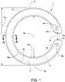
- Heater 1 comprises a C-shaped heater body 2 made from a material such as graphite, ceramics such as SiC, etc.
- the connecting holes 3a and 3b are the points of attachment of an electrical power source which provides the electric current to the heater 1.
- the heater body 2 can have a cross-section width W of about 20 mm, a height H of about 6 mm, an inner diameter Di of about 100 mm and an outer diameter Do of about 140 mm. These dimensions are exemplary of a suitable size. Other dimensions can be selected when appropriate.
- the heater body 2 has an upper horizontal wall 8 having a smooth and flat top heating surface 4 onto which an object to be heated, such as a wafer, is mounted directly or indirectly via a susceptor, etc.
- a center portion of the underside of the heater body 2 is recessed to form an elongated groove or recess 5 between a pair of opposite vertical side walls or ribs 6a, 6b, said side walls having inner surfaces 9a and 9b which at least partially define recess 5.
- the recess 5 and side walls 6a, 6b extend in an arcuate linear direction of the C-shaped heater body 2 so as to provide an inverted U-shaped cross section along a middle portion 7c of the heater, but not at the end portions of the heater body.
- the recess 5 terminates at end surfaces 5a and 5b, the portion of the body between recess end surfaces 5a and 5b and the respective exterior end surfaces 1a and 1b defining the respective end portions of the body.
- the underside of the heater body having 20 mm width comprises the recess 5 having 16 mm width and the opposite side walls 6a, 6b, each having 2 mm width.
- the recess 5 is 4 mm deep from the underside of the heater body 2, leaving the upper horizontal wall 8 of 2 mm thickness.
- body 2 has the same width W along its entire length, including both end portions and the middle portion 7c therebetween.
- the heater of the present invention is particularly advantageous in semiconductor wafer processing applications.
- the full thickness of the body 2 at the end portions maintains a relatively cooler temperature at the end portions but the uniform width of the body improves control of the heat distribution pattern.
- the middle portion 7c of the body has a reduced cross sectional area available for electrical conduction thereby increasing, and improving heater resistance.
- a heater was fabricated in accordance with this invention having a width of 20 mm and a height of 6 mm, and which exhibited a resistance 0.09 ⁇ .
- a control heater made of the same type material and having a width of 20 mm width and height of 6 mm, but fabricated without a recess 5 and ribs 6a, 6b, exhibited a resistance of 0.04 ⁇ .
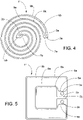
- the heater body is C-shaped in the illustrated embodiment, but in many cases, the heater body can be designed into a spiral heat pattern, such as heater 1' shown in Fig. 4 , and as shown in Japanese patent publication No. 2005-86117(A ), for uniform heating to the wafer or any other object to be heated.
- the heater body is formed into a square or rectangular pattern, such as heater 1" shown in Fig. 5 . These and other heater shapes are also within the scope of the present invention.
- Resistance heater 41 may include a generally a C-shaped heater body 42.
- the heater body 42 may be made from any appropriate material, such as by way of a non-limiting example, graphite, ceramics such as SiC, etc.
- the heater body 42 may include terminal connecting holes 43a, 43b, which may be located at respective end portions of the C-shaped heater body 42.
- the opposing exterior end surfaces 47a and 47b may be generally spaced apart so as to define a gap G2 between such.
- the connecting holes 43a and 43b may be the points of attachment of an electrical power source (not shown) that may provide the electric current to the resistance heater 41.
- the heater body 42 may have a cross-sectional shape such as shown in FIG. 7 .
- the heater body 42 may have a generally horizontally symmetrical cross-sectional shape, such as by way of a non-limiting example, a generally H-shaped cross-sectional shape.
- the heater body 42 may include a generally centrally positioned and generally horizontal wall 48.
- a top and bottom central portion 51, 53 of the heater body 42 may be recessed to form a pair of elongated grooves or recesses 45a, 45b between a pair of opposite vertical side walls or ribs 46a, 46b.
- the recesses 45a, 45b may be positioned on both the top and bottom portion of the heater body 42.
- the side walls 46a, 46b may each include inner surfaces 49a, 49b, 49c and 49d, which may at least partially define the recesses 45a, 45b.
- the recesses 45a, 45b and side walls 46a, 46b may extend in an arcuate linear direction of the generally C-shaped heater body 42.
- This may provide a generally H-shaped cross sectional shape along at least a middle portion 47c of the resistance heater 41.
- the vertical side walls 46a, 46b may each possess a generally smooth and flat heating surface 44a, 44b, respectively onto which an object to be heated, such as a wafer, may be mounted directly or indirectly via a susceptor, etc.
- the general H-shaped cross-sectional shape may not extend to the end portions 47a, 47b of the heater body 42.
- the recesses 45a, 45b may generally terminate at end surfaces 55a and 55b, the portion of the body 42 between recess end surfaces 55a and 55b and the respective exterior end surfaces 47a and 47b may define the respective end portions 57a, 57b of the body 42.
- the topside and underside of the heater body 42 may have a width W of approximately 20 mm, which may include the recesses 45a, 45b having a width of approximately 16 mm and the opposite side walls 46a, 46b each having a width of approximately 6 mm.
- the recesses 45a, 45b may be approximately 2 mm deep from the topside and underside of the heater body 42, leaving the central horizontal wall 48 of a thickness of approximately 2 mm.
- the body 42 may have width W along its entire length, including both end portions and the middle portion 47c therebetween.
- the width W may be generally consistent along an entire length of the body 42. In some embodiments, the width W may be approximately 20 mm. While the exemplary dimensions are described above, the present teachings are not limited to these specific dimensions. The dimensions are merely exemplary and may be altered as required.
- Resistance heater 61 may include a generally a C-shaped heater body 62.
- the heater body 62 may be made from any appropriate material, such as by way of a non-limiting example, graphite, ceramics such as SiC, etc.
- the heater body 62 may include terminal connecting holes 63a, 63b, which may be located at respective end portions of the C-shaped heater body 62.
- the opposing exterior end surfaces 67a and 67b may be generally spaced apart so as to define a gap G3 between such.
- the connecting holes 63a and 63b may be the points of attachment of an electrical power source (not shown) that may provide the electric current to the resistance heater 61.
- the heater body 62 may have a cross-sectional shape such as shown in FIG. 9 .
- the heater body 62 may have a generally symmetrical cross-sectional shape, such as by way of a non-limiting example, a generally I-shaped cross-sectional shape. Still further, the heater body 62 may have a generally horizontally symmetrical cross-sectional shape. In these embodiments, the heater body 62 may include a pair of generally horizontal walls 68a and 68b. The first wall 68a may be on the top portion of the body 62 and the second wall 68b may be on the bottom portion of the body 62. Either or both of the horizontal walls 68a and 68b may possess a generally smooth and flat heating surface 64 onto which an object to be heated, such as a wafer, may be mounted directly or indirectly via a susceptor, etc.
- a pair of side walls 66a, 66b of the heater body 62 may be recessed to form a pair of elongated grooves or recesses 65a, 65b.
- the recesses 65a, 65b may be formed in the pair of opposite vertical side walls 66a, 66b in any appropriate manner.
- a generally central wall 72 may be formed in the heater body 62. This may define the generally I-shaped cross-sectional heater body 42. Side walls 73a, 73b of the central wall 72 may define the recesses 65a, 65b.
- the recesses 65a, 65b and side walls 73a, 73b may extend in an arcuate linear direction of the generally C-shaped heater body 62 so as to provide a generally I-shaped cross sectional shape along at least a middle portion 67c of the resistance heater 61.
- the generally I-shaped cross-sectional shape may not extend to the end portions 75a, 75b of the heater body 62.
- the recess 65a, 65b may terminate at end surfaces 75a and 75b.
- the portion of the body 62 between recess end surfaces 75a and 75b and the respective exterior end surfaces 67a and 67b may define the respective end portions 77a, 77b of the body 62.
- the topside and underside of the heater body 62 may have a width of approximately 20 mm, which may include the recesses 65a, 65b having a height of approximately 2 mm a depth of approximately 7 mm from the vertical side walls 66a, 66b of the heater body 62. This may result in the thickness of walls 68a and 68b at the recesses 65a, 65b each being approximately 2 mm.
- the central wall 72 may have a width of approximately 6 mm and a thickness of approximately 6 mm.
- the body 62 may have width W along its entire length, including both end portions 77a, 77b and the middle portion 67c therebetween.
- the width W may be generally consistent along an entire length of the body 62 and may be approximately 20 mm. While the exemplary dimensions are described above, the present teachings are not limited to these specific dimensions. The dimensions are merely exemplary and may be altered as required.
Applications Claiming Priority (2)
| Application Number | Priority Date | Filing Date | Title |
|---|---|---|---|
| US13/424,947 US8993939B2 (en) | 2008-01-18 | 2012-03-20 | Resistance heater |
| PCT/US2013/033139 WO2013142594A1 (en) | 2012-03-20 | 2013-03-20 | Resistance heater |
Publications (3)
| Publication Number | Publication Date |
|---|---|
| EP2829155A1 EP2829155A1 (en) | 2015-01-28 |
| EP2829155A4 EP2829155A4 (en) | 2015-07-15 |
| EP2829155B1 true EP2829155B1 (en) | 2022-09-07 |
Family
ID=49223322
Family Applications (1)
| Application Number | Title | Priority Date | Filing Date |
|---|---|---|---|
| EP13764286.4A Active EP2829155B1 (en) | 2012-03-20 | 2013-03-20 | Resistance heater |
Country Status (4)
| Country | Link |
|---|---|
| EP (1) | EP2829155B1 (zh) |
| JP (1) | JP6537964B2 (zh) |
| CN (1) | CN104206003B (zh) |
| WO (1) | WO2013142594A1 (zh) |
Cited By (1)
| Publication number | Priority date | Publication date | Assignee | Title |
|---|---|---|---|---|
| US20220053612A1 (en) * | 2018-09-13 | 2022-02-17 | De Luca Oven Technologies, Llc | Heater element incorporating primary conductor for use in a high-speed oven |
Families Citing this family (3)
| Publication number | Priority date | Publication date | Assignee | Title |
|---|---|---|---|---|
| US11873098B2 (en) * | 2018-10-22 | 2024-01-16 | Goodrich Corporation | Heater design for carbon allotrope ice protection systems |
| CA3054177A1 (en) * | 2018-10-22 | 2020-04-22 | Goodrich Corporation | Heater design for carbon allotrope ice protection systems |
| JP2022515529A (ja) * | 2018-12-27 | 2022-02-18 | モメンティブ パフォーマンス マテリアルズ クオーツ インコーポレイテッド | 窒化ホウ素および二ホウ化チタンを含むセラミック複合体ヒーター |
Citations (1)
| Publication number | Priority date | Publication date | Assignee | Title |
|---|---|---|---|---|
| US4147888A (en) * | 1977-07-20 | 1979-04-03 | Seiki Sato | Electric heating element for electric resistance furnaces |
Family Cites Families (6)
| Publication number | Priority date | Publication date | Assignee | Title |
|---|---|---|---|---|
| US6285011B1 (en) * | 1999-10-12 | 2001-09-04 | Memc Electronic Materials, Inc. | Electrical resistance heater for crystal growing apparatus |
| JP4671262B2 (ja) * | 2003-01-21 | 2011-04-13 | 日本碍子株式会社 | 半導体加熱装置 |
| US20050217799A1 (en) * | 2004-03-31 | 2005-10-06 | Tokyo Electron Limited | Wafer heater assembly |
| JP4690297B2 (ja) * | 2006-12-01 | 2011-06-01 | モメンティブ・パフォーマンス・マテリアルズ・ジャパン合同会社 | ヒータ |
| US8164028B2 (en) * | 2008-01-18 | 2012-04-24 | Momentive Performance Materials Inc. | Resistance heater |
| EP2141490B1 (en) * | 2008-07-02 | 2015-04-01 | Stichting IMEC Nederland | Chemical sensing microbeam device |
-
2013
- 2013-03-20 JP JP2015501882A patent/JP6537964B2/ja active Active
- 2013-03-20 CN CN201380015871.4A patent/CN104206003B/zh active Active
- 2013-03-20 EP EP13764286.4A patent/EP2829155B1/en active Active
- 2013-03-20 WO PCT/US2013/033139 patent/WO2013142594A1/en active Application Filing
Patent Citations (1)
| Publication number | Priority date | Publication date | Assignee | Title |
|---|---|---|---|---|
| US4147888A (en) * | 1977-07-20 | 1979-04-03 | Seiki Sato | Electric heating element for electric resistance furnaces |
Cited By (1)
| Publication number | Priority date | Publication date | Assignee | Title |
|---|---|---|---|---|
| US20220053612A1 (en) * | 2018-09-13 | 2022-02-17 | De Luca Oven Technologies, Llc | Heater element incorporating primary conductor for use in a high-speed oven |
Also Published As
| Publication number | Publication date |
|---|---|
| WO2013142594A1 (en) | 2013-09-26 |
| EP2829155A4 (en) | 2015-07-15 |
| JP6537964B2 (ja) | 2019-07-03 |
| CN104206003A (zh) | 2014-12-10 |
| JP2015518627A (ja) | 2015-07-02 |
| CN104206003B (zh) | 2016-10-12 |
| EP2829155A1 (en) | 2015-01-28 |
Similar Documents
| Publication | Publication Date | Title |
|---|---|---|
| US8993939B2 (en) | Resistance heater | |
| EP2829155B1 (en) | Resistance heater | |
| KR102026727B1 (ko) | 히터를 구비한 기판 지지체 | |
| KR100709536B1 (ko) | 가열 장치 | |
| US8193473B2 (en) | Uniform temperature heater | |
| KR20040107477A (ko) | 서셉터를 포함한 처리 챔버에서 반도체 기판을 가열하기위한 공정 및 시스템 | |
| JP2019508862A (ja) | 円筒状ヒータ | |
| CN111869318A (zh) | 多区域加热器 | |
| US20150173127A1 (en) | Heating wire arrangement for ceramic heater | |
| JP4690297B2 (ja) | ヒータ | |
| JP6059512B2 (ja) | ヒータユニット | |
| US8164028B2 (en) | Resistance heater | |
| CN113195780B (zh) | 具有不均匀的纵向截面的用于半导体材料的外延反应器的反应室及反应器 | |
| CN106929802B (zh) | 用于加热坩埚的加热器设备和用于蒸发或升华材料的系统 | |
| JP7331107B2 (ja) | 半導体製造装置用部材 | |
| JP2005519427A (ja) | けい化モリブデン型のエレメント | |
| KR100650988B1 (ko) | 챔버 내에 열전도성 장벽이 구비된 저온 전기로 | |
| KR20190035857A (ko) | 비-균일한 절연부를 갖는 열적 프로세스 디바이스 | |
| KR101363027B1 (ko) | 세라믹 히터용 열선 커넥팅 구조. | |
| KR101333227B1 (ko) | 세라믹 히터용 전극 커넥팅 구조. | |
| KR20200123633A (ko) | 온도 편차 감소용 단열부재가 구비된 소결로 | |
| KR102273562B1 (ko) | 반도체 히팅장치 | |
| KR20230083898A (ko) | 반도체 제조 장치용 가열 장치 | |
| KR102273563B1 (ko) | 히팅장치를 이용한 소재 가열방법 | |
| US20230187187A1 (en) | Wafer placement table |
Legal Events
| Date | Code | Title | Description |
|---|---|---|---|
| PUAI | Public reference made under article 153(3) epc to a published international application that has entered the european phase |
Free format text: ORIGINAL CODE: 0009012 |
|
| 17P | Request for examination filed |
Effective date: 20140925 |
|
| AK | Designated contracting states |
Kind code of ref document: A1 Designated state(s): AL AT BE BG CH CY CZ DE DK EE ES FI FR GB GR HR HU IE IS IT LI LT LU LV MC MK MT NL NO PL PT RO RS SE SI SK SM TR |
|
| AX | Request for extension of the european patent |
Extension state: BA ME |
|
| RIN1 | Information on inventor provided before grant (corrected) |
Inventor name: OTAKA, AKINOBU Inventor name: LU, ZHONG-HAO Inventor name: MATSUI, YOSHIHIKO Inventor name: FUJIMURA, KENSUKE Inventor name: HIGUCHI, TAKESHI Inventor name: MORIKAWA, YUJI |
|
| DAX | Request for extension of the european patent (deleted) | ||
| RA4 | Supplementary search report drawn up and despatched (corrected) |
Effective date: 20150611 |
|
| RIC1 | Information provided on ipc code assigned before grant |
Ipc: H05B 3/20 20060101AFI20150605BHEP Ipc: H05B 3/24 20060101ALI20150605BHEP Ipc: H01L 21/67 20060101ALI20150605BHEP Ipc: H05B 3/14 20060101ALI20150605BHEP |
|
| RAP1 | Party data changed (applicant data changed or rights of an application transferred) |
Owner name: MOMENTIVE PERFORMANCE MATERIALS INC. |
|
| 17Q | First examination report despatched |
Effective date: 20151221 |
|
| STAA | Information on the status of an ep patent application or granted ep patent |
Free format text: STATUS: EXAMINATION IS IN PROGRESS |
|
| STAA | Information on the status of an ep patent application or granted ep patent |
Free format text: STATUS: EXAMINATION IS IN PROGRESS |
|
| RAP1 | Party data changed (applicant data changed or rights of an application transferred) |
Owner name: MOMENTIVE PERFORMANCE MATERIALS QUARTZ, INC. |
|
| GRAP | Despatch of communication of intention to grant a patent |
Free format text: ORIGINAL CODE: EPIDOSNIGR1 |
|
| STAA | Information on the status of an ep patent application or granted ep patent |
Free format text: STATUS: GRANT OF PATENT IS INTENDED |
|
| INTG | Intention to grant announced |
Effective date: 20220330 |
|
| GRAS | Grant fee paid |
Free format text: ORIGINAL CODE: EPIDOSNIGR3 |
|
| GRAA | (expected) grant |
Free format text: ORIGINAL CODE: 0009210 |
|
| STAA | Information on the status of an ep patent application or granted ep patent |
Free format text: STATUS: THE PATENT HAS BEEN GRANTED |
|
| AK | Designated contracting states |
Kind code of ref document: B1 Designated state(s): AL AT BE BG CH CY CZ DE DK EE ES FI FR GB GR HR HU IE IS IT LI LT LU LV MC MK MT NL NO PL PT RO RS SE SI SK SM TR |
|
| REG | Reference to a national code |
Ref country code: GB Ref legal event code: FG4D |
|
| REG | Reference to a national code |
Ref country code: CH Ref legal event code: EP Ref country code: AT Ref legal event code: REF Ref document number: 1518111 Country of ref document: AT Kind code of ref document: T Effective date: 20220915 |
|
| REG | Reference to a national code |
Ref country code: IE Ref legal event code: FG4D |
|
| REG | Reference to a national code |
Ref country code: DE Ref legal event code: R096 Ref document number: 602013082471 Country of ref document: DE |
|
| REG | Reference to a national code |
Ref country code: FI Ref legal event code: FGE |
|
| REG | Reference to a national code |
Ref country code: NL Ref legal event code: FP |
|
| REG | Reference to a national code |
Ref country code: LT Ref legal event code: MG9D |
|
| PG25 | Lapsed in a contracting state [announced via postgrant information from national office to epo] |
Ref country code: SE Free format text: LAPSE BECAUSE OF FAILURE TO SUBMIT A TRANSLATION OF THE DESCRIPTION OR TO PAY THE FEE WITHIN THE PRESCRIBED TIME-LIMIT Effective date: 20220907 Ref country code: RS Free format text: LAPSE BECAUSE OF FAILURE TO SUBMIT A TRANSLATION OF THE DESCRIPTION OR TO PAY THE FEE WITHIN THE PRESCRIBED TIME-LIMIT Effective date: 20220907 Ref country code: NO Free format text: LAPSE BECAUSE OF FAILURE TO SUBMIT A TRANSLATION OF THE DESCRIPTION OR TO PAY THE FEE WITHIN THE PRESCRIBED TIME-LIMIT Effective date: 20221207 Ref country code: LV Free format text: LAPSE BECAUSE OF FAILURE TO SUBMIT A TRANSLATION OF THE DESCRIPTION OR TO PAY THE FEE WITHIN THE PRESCRIBED TIME-LIMIT Effective date: 20220907 Ref country code: LT Free format text: LAPSE BECAUSE OF FAILURE TO SUBMIT A TRANSLATION OF THE DESCRIPTION OR TO PAY THE FEE WITHIN THE PRESCRIBED TIME-LIMIT Effective date: 20220907 Ref country code: ES Free format text: LAPSE BECAUSE OF FAILURE TO SUBMIT A TRANSLATION OF THE DESCRIPTION OR TO PAY THE FEE WITHIN THE PRESCRIBED TIME-LIMIT Effective date: 20220907 |
|
| REG | Reference to a national code |
Ref country code: AT Ref legal event code: MK05 Ref document number: 1518111 Country of ref document: AT Kind code of ref document: T Effective date: 20220907 |
|
| PG25 | Lapsed in a contracting state [announced via postgrant information from national office to epo] |
Ref country code: HR Free format text: LAPSE BECAUSE OF FAILURE TO SUBMIT A TRANSLATION OF THE DESCRIPTION OR TO PAY THE FEE WITHIN THE PRESCRIBED TIME-LIMIT Effective date: 20220907 Ref country code: GR Free format text: LAPSE BECAUSE OF FAILURE TO SUBMIT A TRANSLATION OF THE DESCRIPTION OR TO PAY THE FEE WITHIN THE PRESCRIBED TIME-LIMIT Effective date: 20221208 |
|
| PG25 | Lapsed in a contracting state [announced via postgrant information from national office to epo] |
Ref country code: SM Free format text: LAPSE BECAUSE OF FAILURE TO SUBMIT A TRANSLATION OF THE DESCRIPTION OR TO PAY THE FEE WITHIN THE PRESCRIBED TIME-LIMIT Effective date: 20220907 Ref country code: RO Free format text: LAPSE BECAUSE OF FAILURE TO SUBMIT A TRANSLATION OF THE DESCRIPTION OR TO PAY THE FEE WITHIN THE PRESCRIBED TIME-LIMIT Effective date: 20220907 Ref country code: PT Free format text: LAPSE BECAUSE OF FAILURE TO SUBMIT A TRANSLATION OF THE DESCRIPTION OR TO PAY THE FEE WITHIN THE PRESCRIBED TIME-LIMIT Effective date: 20230109 Ref country code: CZ Free format text: LAPSE BECAUSE OF FAILURE TO SUBMIT A TRANSLATION OF THE DESCRIPTION OR TO PAY THE FEE WITHIN THE PRESCRIBED TIME-LIMIT Effective date: 20220907 Ref country code: AT Free format text: LAPSE BECAUSE OF FAILURE TO SUBMIT A TRANSLATION OF THE DESCRIPTION OR TO PAY THE FEE WITHIN THE PRESCRIBED TIME-LIMIT Effective date: 20220907 |
|
| PGFP | Annual fee paid to national office [announced via postgrant information from national office to epo] |
Ref country code: FR Payment date: 20230323 Year of fee payment: 11 Ref country code: FI Payment date: 20230323 Year of fee payment: 11 |
|
| PG25 | Lapsed in a contracting state [announced via postgrant information from national office to epo] |
Ref country code: SK Free format text: LAPSE BECAUSE OF FAILURE TO SUBMIT A TRANSLATION OF THE DESCRIPTION OR TO PAY THE FEE WITHIN THE PRESCRIBED TIME-LIMIT Effective date: 20220907 Ref country code: PL Free format text: LAPSE BECAUSE OF FAILURE TO SUBMIT A TRANSLATION OF THE DESCRIPTION OR TO PAY THE FEE WITHIN THE PRESCRIBED TIME-LIMIT Effective date: 20220907 Ref country code: IS Free format text: LAPSE BECAUSE OF FAILURE TO SUBMIT A TRANSLATION OF THE DESCRIPTION OR TO PAY THE FEE WITHIN THE PRESCRIBED TIME-LIMIT Effective date: 20230107 Ref country code: EE Free format text: LAPSE BECAUSE OF FAILURE TO SUBMIT A TRANSLATION OF THE DESCRIPTION OR TO PAY THE FEE WITHIN THE PRESCRIBED TIME-LIMIT Effective date: 20220907 |
|
| PGFP | Annual fee paid to national office [announced via postgrant information from national office to epo] |
Ref country code: IT Payment date: 20230321 Year of fee payment: 11 Ref country code: GB Payment date: 20230321 Year of fee payment: 11 Ref country code: DE Payment date: 20230328 Year of fee payment: 11 |
|
| REG | Reference to a national code |
Ref country code: DE Ref legal event code: R097 Ref document number: 602013082471 Country of ref document: DE |
|
| PG25 | Lapsed in a contracting state [announced via postgrant information from national office to epo] |
Ref country code: AL Free format text: LAPSE BECAUSE OF FAILURE TO SUBMIT A TRANSLATION OF THE DESCRIPTION OR TO PAY THE FEE WITHIN THE PRESCRIBED TIME-LIMIT Effective date: 20220907 |
|
| PGFP | Annual fee paid to national office [announced via postgrant information from national office to epo] |
Ref country code: NL Payment date: 20230323 Year of fee payment: 11 |
|
| P01 | Opt-out of the competence of the unified patent court (upc) registered |
Effective date: 20230601 |
|
| PLBE | No opposition filed within time limit |
Free format text: ORIGINAL CODE: 0009261 |
|
| STAA | Information on the status of an ep patent application or granted ep patent |
Free format text: STATUS: NO OPPOSITION FILED WITHIN TIME LIMIT |
|
| PG25 | Lapsed in a contracting state [announced via postgrant information from national office to epo] |
Ref country code: DK Free format text: LAPSE BECAUSE OF FAILURE TO SUBMIT A TRANSLATION OF THE DESCRIPTION OR TO PAY THE FEE WITHIN THE PRESCRIBED TIME-LIMIT Effective date: 20220907 |
|
| 26N | No opposition filed |
Effective date: 20230608 |
|
| PG25 | Lapsed in a contracting state [announced via postgrant information from national office to epo] |
Ref country code: SI Free format text: LAPSE BECAUSE OF FAILURE TO SUBMIT A TRANSLATION OF THE DESCRIPTION OR TO PAY THE FEE WITHIN THE PRESCRIBED TIME-LIMIT Effective date: 20220907 |
|
| PG25 | Lapsed in a contracting state [announced via postgrant information from national office to epo] |
Ref country code: MC Free format text: LAPSE BECAUSE OF FAILURE TO SUBMIT A TRANSLATION OF THE DESCRIPTION OR TO PAY THE FEE WITHIN THE PRESCRIBED TIME-LIMIT Effective date: 20220907 |
|
| REG | Reference to a national code |
Ref country code: CH Ref legal event code: PL |
|
| REG | Reference to a national code |
Ref country code: BE Ref legal event code: MM Effective date: 20230331 |
|
| PG25 | Lapsed in a contracting state [announced via postgrant information from national office to epo] |
Ref country code: LU Free format text: LAPSE BECAUSE OF NON-PAYMENT OF DUE FEES Effective date: 20230320 |
|
| REG | Reference to a national code |
Ref country code: IE Ref legal event code: MM4A |
|
| PG25 | Lapsed in a contracting state [announced via postgrant information from national office to epo] |
Ref country code: LI Free format text: LAPSE BECAUSE OF NON-PAYMENT OF DUE FEES Effective date: 20230331 Ref country code: IE Free format text: LAPSE BECAUSE OF NON-PAYMENT OF DUE FEES Effective date: 20230320 Ref country code: CH Free format text: LAPSE BECAUSE OF NON-PAYMENT OF DUE FEES Effective date: 20230331 |
|
| PG25 | Lapsed in a contracting state [announced via postgrant information from national office to epo] |
Ref country code: BE Free format text: LAPSE BECAUSE OF NON-PAYMENT OF DUE FEES Effective date: 20230331 |
|
| PGFP | Annual fee paid to national office [announced via postgrant information from national office to epo] |
Ref country code: NL Payment date: 20240326 Year of fee payment: 12 |