EP2827192B1 - Continuously producing digital micro-scale patterns on a thin polymer film - Google Patents
Continuously producing digital micro-scale patterns on a thin polymer film Download PDFInfo
- Publication number
- EP2827192B1 EP2827192B1 EP14177409.1A EP14177409A EP2827192B1 EP 2827192 B1 EP2827192 B1 EP 2827192B1 EP 14177409 A EP14177409 A EP 14177409A EP 2827192 B1 EP2827192 B1 EP 2827192B1
- Authority
- EP
- European Patent Office
- Prior art keywords
- conveyor
- patterned
- thin film
- micro
- gap region
- Prior art date
- Legal status (The legal status is an assumption and is not a legal conclusion. Google has not performed a legal analysis and makes no representation as to the accuracy of the status listed.)
- Not-in-force
Links
- 229920006254 polymer film Polymers 0.000 title claims description 12
- 229920000642 polymer Polymers 0.000 claims description 97
- 239000010409 thin film Substances 0.000 claims description 81
- 239000007788 liquid Substances 0.000 claims description 75
- 230000005684 electric field Effects 0.000 claims description 58
- 238000000059 patterning Methods 0.000 claims description 36
- 238000001723 curing Methods 0.000 claims description 25
- 230000007246 mechanism Effects 0.000 claims description 18
- 239000002086 nanomaterial Substances 0.000 claims description 15
- 239000007787 solid Substances 0.000 claims description 11
- 238000000576 coating method Methods 0.000 claims description 10
- 238000011144 upstream manufacturing Methods 0.000 claims description 9
- 239000011248 coating agent Substances 0.000 claims description 8
- 238000001029 thermal curing Methods 0.000 claims description 7
- 239000004020 conductor Substances 0.000 claims description 6
- 239000003989 dielectric material Substances 0.000 claims description 5
- 239000011810 insulating material Substances 0.000 claims description 3
- 239000004065 semiconductor Substances 0.000 claims description 3
- 238000007766 curtain coating Methods 0.000 claims description 2
- 238000007767 slide coating Methods 0.000 claims description 2
- 238000007764 slot die coating Methods 0.000 claims description 2
- 238000001816 cooling Methods 0.000 claims 1
- 238000000034 method Methods 0.000 description 26
- 238000004519 manufacturing process Methods 0.000 description 16
- 230000015572 biosynthetic process Effects 0.000 description 12
- 230000008569 process Effects 0.000 description 10
- 239000010408 film Substances 0.000 description 8
- 239000000463 material Substances 0.000 description 8
- 239000002245 particle Substances 0.000 description 8
- 239000002861 polymer material Substances 0.000 description 8
- 238000013459 approach Methods 0.000 description 7
- 238000001459 lithography Methods 0.000 description 4
- OKTJSMMVPCPJKN-UHFFFAOYSA-N Carbon Chemical compound [C] OKTJSMMVPCPJKN-UHFFFAOYSA-N 0.000 description 3
- 230000008901 benefit Effects 0.000 description 3
- 239000002041 carbon nanotube Substances 0.000 description 3
- 229910021393 carbon nanotube Inorganic materials 0.000 description 3
- 239000003814 drug Substances 0.000 description 3
- 239000012530 fluid Substances 0.000 description 3
- 229910052751 metal Inorganic materials 0.000 description 3
- 239000002184 metal Substances 0.000 description 3
- 238000012545 processing Methods 0.000 description 3
- 239000012780 transparent material Substances 0.000 description 3
- 239000002202 Polyethylene glycol Substances 0.000 description 2
- 239000004372 Polyvinyl alcohol Substances 0.000 description 2
- GWEVSGVZZGPLCZ-UHFFFAOYSA-N Titan oxide Chemical compound O=[Ti]=O GWEVSGVZZGPLCZ-UHFFFAOYSA-N 0.000 description 2
- 230000003213 activating effect Effects 0.000 description 2
- 230000001419 dependent effect Effects 0.000 description 2
- 238000000151 deposition Methods 0.000 description 2
- 230000008021 deposition Effects 0.000 description 2
- 238000010586 diagram Methods 0.000 description 2
- 229940079593 drug Drugs 0.000 description 2
- 238000005516 engineering process Methods 0.000 description 2
- 239000000203 mixture Substances 0.000 description 2
- 239000002070 nanowire Substances 0.000 description 2
- 230000003287 optical effect Effects 0.000 description 2
- 108091008695 photoreceptors Proteins 0.000 description 2
- 229920001223 polyethylene glycol Polymers 0.000 description 2
- 229920002451 polyvinyl alcohol Polymers 0.000 description 2
- 229920000036 polyvinylpyrrolidone Polymers 0.000 description 2
- 239000001267 polyvinylpyrrolidone Substances 0.000 description 2
- 235000013855 polyvinylpyrrolidone Nutrition 0.000 description 2
- 239000002243 precursor Substances 0.000 description 2
- 230000007261 regionalization Effects 0.000 description 2
- 230000035945 sensitivity Effects 0.000 description 2
- 229920001187 thermosetting polymer Polymers 0.000 description 2
- 229910001218 Gallium arsenide Inorganic materials 0.000 description 1
- 239000004793 Polystyrene Substances 0.000 description 1
- 238000003848 UV Light-Curing Methods 0.000 description 1
- 239000000853 adhesive Substances 0.000 description 1
- 230000001070 adhesive effect Effects 0.000 description 1
- 239000006117 anti-reflective coating Substances 0.000 description 1
- 238000003491 array Methods 0.000 description 1
- 230000005540 biological transmission Effects 0.000 description 1
- 230000008859 change Effects 0.000 description 1
- 239000003795 chemical substances by application Substances 0.000 description 1
- 229920001940 conductive polymer Polymers 0.000 description 1
- 238000012937 correction Methods 0.000 description 1
- 230000007423 decrease Effects 0.000 description 1
- 230000003247 decreasing effect Effects 0.000 description 1
- 238000013461 design Methods 0.000 description 1
- 230000009969 flowable effect Effects 0.000 description 1
- 239000011521 glass Substances 0.000 description 1
- 238000010438 heat treatment Methods 0.000 description 1
- 230000002209 hydrophobic effect Effects 0.000 description 1
- 230000006872 improvement Effects 0.000 description 1
- AMGQUBHHOARCQH-UHFFFAOYSA-N indium;oxotin Chemical compound [In].[Sn]=O AMGQUBHHOARCQH-UHFFFAOYSA-N 0.000 description 1
- 230000003993 interaction Effects 0.000 description 1
- 238000000025 interference lithography Methods 0.000 description 1
- 238000011031 large-scale manufacturing process Methods 0.000 description 1
- 238000013532 laser treatment Methods 0.000 description 1
- 238000005461 lubrication Methods 0.000 description 1
- 238000003754 machining Methods 0.000 description 1
- 230000000873 masking effect Effects 0.000 description 1
- 238000005259 measurement Methods 0.000 description 1
- 238000002844 melting Methods 0.000 description 1
- 230000008018 melting Effects 0.000 description 1
- 238000012986 modification Methods 0.000 description 1
- 230000004048 modification Effects 0.000 description 1
- 239000003607 modifier Substances 0.000 description 1
- 238000001127 nanoimprint lithography Methods 0.000 description 1
- 239000002071 nanotube Substances 0.000 description 1
- 230000002093 peripheral effect Effects 0.000 description 1
- 229920002120 photoresistant polymer Polymers 0.000 description 1
- 229920002223 polystyrene Polymers 0.000 description 1
- 238000013442 quality metrics Methods 0.000 description 1
- 230000005855 radiation Effects 0.000 description 1
- 230000010076 replication Effects 0.000 description 1
- 230000004044 response Effects 0.000 description 1
- 238000012776 robust process Methods 0.000 description 1
- 238000005096 rolling process Methods 0.000 description 1
- 238000007493 shaping process Methods 0.000 description 1
- 125000006850 spacer group Chemical group 0.000 description 1
- 239000013077 target material Substances 0.000 description 1
- 230000002123 temporal effect Effects 0.000 description 1
- 238000007669 thermal treatment Methods 0.000 description 1
- 239000004634 thermosetting polymer Substances 0.000 description 1
- 238000000427 thin-film deposition Methods 0.000 description 1
- 239000004408 titanium dioxide Substances 0.000 description 1
- 238000009736 wetting Methods 0.000 description 1
Images


Classifications
-
- G—PHYSICS
- G03—PHOTOGRAPHY; CINEMATOGRAPHY; ANALOGOUS TECHNIQUES USING WAVES OTHER THAN OPTICAL WAVES; ELECTROGRAPHY; HOLOGRAPHY
- G03F—PHOTOMECHANICAL PRODUCTION OF TEXTURED OR PATTERNED SURFACES, e.g. FOR PRINTING, FOR PROCESSING OF SEMICONDUCTOR DEVICES; MATERIALS THEREFOR; ORIGINALS THEREFOR; APPARATUS SPECIALLY ADAPTED THEREFOR
- G03F7/00—Photomechanical, e.g. photolithographic, production of textured or patterned surfaces, e.g. printing surfaces; Materials therefor, e.g. comprising photoresists; Apparatus specially adapted therefor
- G03F7/70—Microphotolithographic exposure; Apparatus therefor
-
- B—PERFORMING OPERATIONS; TRANSPORTING
- B05—SPRAYING OR ATOMISING IN GENERAL; APPLYING FLUENT MATERIALS TO SURFACES, IN GENERAL
- B05C—APPARATUS FOR APPLYING FLUENT MATERIALS TO SURFACES, IN GENERAL
- B05C5/00—Apparatus in which liquid or other fluent material is projected, poured or allowed to flow on to the surface of the work
- B05C5/005—Curtain coaters
-
- B—PERFORMING OPERATIONS; TRANSPORTING
- B05—SPRAYING OR ATOMISING IN GENERAL; APPLYING FLUENT MATERIALS TO SURFACES, IN GENERAL
- B05C—APPARATUS FOR APPLYING FLUENT MATERIALS TO SURFACES, IN GENERAL
- B05C5/00—Apparatus in which liquid or other fluent material is projected, poured or allowed to flow on to the surface of the work
- B05C5/007—Slide-hopper coaters, i.e. apparatus in which the liquid or other fluent material flows freely on an inclined surface before contacting the work
-
- B—PERFORMING OPERATIONS; TRANSPORTING
- B05—SPRAYING OR ATOMISING IN GENERAL; APPLYING FLUENT MATERIALS TO SURFACES, IN GENERAL
- B05C—APPARATUS FOR APPLYING FLUENT MATERIALS TO SURFACES, IN GENERAL
- B05C9/00—Apparatus or plant for applying liquid or other fluent material to surfaces by means not covered by any preceding group, or in which the means of applying the liquid or other fluent material is not important
- B05C9/08—Apparatus or plant for applying liquid or other fluent material to surfaces by means not covered by any preceding group, or in which the means of applying the liquid or other fluent material is not important for applying liquid or other fluent material and performing an auxiliary operation
- B05C9/12—Apparatus or plant for applying liquid or other fluent material to surfaces by means not covered by any preceding group, or in which the means of applying the liquid or other fluent material is not important for applying liquid or other fluent material and performing an auxiliary operation the auxiliary operation being performed after the application
-
- G—PHYSICS
- G03—PHOTOGRAPHY; CINEMATOGRAPHY; ANALOGOUS TECHNIQUES USING WAVES OTHER THAN OPTICAL WAVES; ELECTROGRAPHY; HOLOGRAPHY
- G03F—PHOTOMECHANICAL PRODUCTION OF TEXTURED OR PATTERNED SURFACES, e.g. FOR PRINTING, FOR PROCESSING OF SEMICONDUCTOR DEVICES; MATERIALS THEREFOR; ORIGINALS THEREFOR; APPARATUS SPECIALLY ADAPTED THEREFOR
- G03F7/00—Photomechanical, e.g. photolithographic, production of textured or patterned surfaces, e.g. printing surfaces; Materials therefor, e.g. comprising photoresists; Apparatus specially adapted therefor
- G03F7/0002—Lithographic processes using patterning methods other than those involving the exposure to radiation, e.g. by stamping
-
- B—PERFORMING OPERATIONS; TRANSPORTING
- B41—PRINTING; LINING MACHINES; TYPEWRITERS; STAMPS
- B41F—PRINTING MACHINES OR PRESSES
- B41F16/00—Transfer printing apparatus
-
- G—PHYSICS
- G03—PHOTOGRAPHY; CINEMATOGRAPHY; ANALOGOUS TECHNIQUES USING WAVES OTHER THAN OPTICAL WAVES; ELECTROGRAPHY; HOLOGRAPHY
- G03G—ELECTROGRAPHY; ELECTROPHOTOGRAPHY; MAGNETOGRAPHY
- G03G13/00—Electrographic processes using a charge pattern
- G03G13/06—Developing
- G03G13/10—Developing using a liquid developer, e.g. liquid suspension
-
- G—PHYSICS
- G03—PHOTOGRAPHY; CINEMATOGRAPHY; ANALOGOUS TECHNIQUES USING WAVES OTHER THAN OPTICAL WAVES; ELECTROGRAPHY; HOLOGRAPHY
- G03G—ELECTROGRAPHY; ELECTROPHOTOGRAPHY; MAGNETOGRAPHY
- G03G15/00—Apparatus for electrographic processes using a charge pattern
- G03G15/02—Apparatus for electrographic processes using a charge pattern for laying down a uniform charge, e.g. for sensitising; Corona discharge devices
Definitions
- This invention relates to micro-scale patterned structures, and more particularly to systems for producing micro-scale patterned structures.
- Such patterned polymer thin films are useful, e.g., for optical applications (anti-reflective coatings and filters) and controlled wetting applications (hydrophobic and hydrophilic applications).
- Electrohydrodynamic (EHD) patterning is a recently developed technology that involves electrically transferring the micro- or nano-structures formed on a template onto a thin polymer film by shaping the surface of the liquid polymer film through a balance of applied forces on the liquid and the surface tension of the liquid.
- a surface instability can be driven by van der Waals and thermal forces, but is typically dominated by external forces, if those are present. All external (e.g., electrical or thermal) forces that cause a pressure gradient across the interface can cause this surface instability.
- the present invention focuses on EHD patterning techniques applied to polymer thin films having a height/thickness that is much less than the length-scale of the instability, so the kinetics of the polymer thin film are completely described by lubrication theory, and the emerging pattern is driven by the fastest growing capillary wave mode.
- the time scale for generating such polymer thin film EHD patterning is dependent on the liquid polymer's dielectric constant, viscosity, height/thickness and surface tension, the applied voltage (electric field), and the distance between the electrodes or charges used to generate the electric field, and the length scale of the emerging pattern is dependent on the surface tension, and the applied voltage and electric field inside the polymer film.
- EHD patterning can either occur at a length scale that is intrinsic to the film properties if the electric field is constant or be forced into specific structures if the electric field is spatially varied.
- the height of replication for EHD patterning has been limited at the nano-scale in previously proposed techniques because the electric field is sensitive to the spacer height of the template.
- conventional EHD patterning techniques are not commercially viable because they are unable to produce commercially useful quantities of film.
- WO 2007/021130 A1 discloses a patterning method using coatings containing ionic components.
- US 2004/009673 A1 discloses a lithography process for creating patterns in an activating light curable liquid using electric fields followed by curing of the activating light curable liquid.
- Nicoleta E. Voicu et al., XP002624803 discloses titanium dioxide patterning using electrohydrodynamic lithography.
- WO 01/47003 A2 discloses methods and apparatus for forming submicron patterns on films, including applying an electric field to an interface between flowable media having different dielectric properties.
- US 2003/0215577 A1 discloses a method and system for fabricating nanoscale patterns in light curable compositions using an electric field.
- EP2116899 A2 discloses a composition and method for forming an inorganic pattern and patterning via electrohydrodynamic lithography.
- the present invention is directed to systems that implement improved Electrohydrodynamic (EHD) thin film patterning techniques and provide viable and economical manufacturing techniques to continuously producing micro-scale patterned structures that either integrally connected to a thin polymer film or are separated from each other.
- the systems utilize two curved conveyors (e.g., two rollers or two belts) having opposing surfaces that are spaced apart by a relatively large distances on opposite sides of a gap (or nip) region.
- a liquid thin film containing a polymer, a polymer precursor, or another suitable material is coated or otherwise disposed onto one conveyor surface (e.g., the "lower" roller or belt) by a suitable coating mechanism such that it is subsequently conveyed into the gap region, where the minimum gap distance between the two conveyor surfaces is set such a small gap is provided between the upper film surface and the opposing conveyor surface.
- one conveyor surface e.g., the "lower” roller or belt
- the liquid thin film As it passes through the gap region, the liquid thin film is subjected to an electric field generated between the two conveyors, with the electric field strength and liquid thin film characteristics (e.g., viscosity and dielectric constant) being set such that the liquid thin film undergoes EHD patterning (i.e., portions of the liquid polymer are pulled toward the upper conveyor, thereby forming patterned micro-scale liquid polymer features that extend from the lower conveyor into the small gap that is filled with air or another fluid).
- EHD patterning i.e., portions of the liquid polymer are pulled toward the upper conveyor, thereby forming patterned micro-scale liquid polymer features that extend from the lower conveyor into the small gap that is filled with air or another fluid.
- An appropriate curing mechanism e.g., a UV laser or thermal treatment
- cross-link (cure) the polymer thin film while undergoing EHD patterning (e.g., inside the gap region or immediately outside the gap region), whereby the liquid micro-scale polymer features are hardened (solidified) to form micro-scale patterned structures having substantially the same pattern shape that was generated in the liquid polymer by the electric field.
- EHD patterning e.g., inside the gap region or immediately outside the gap region
- the solid micro-scale patterned structures and any adjoining polymer thin film material are then removed from the lower conveyor.
- the thin polymer film contains nanostructures (e.g., nanowires or nanotubes) that become vertically oriented within the micro-scale structures.
- the nanostructures have initial (e.g., random) orientations during thin film formation, but become aligned within the micro-scale patterned structure in a substantially perpendicular orientation relative to the underlying conveyor surface in response to the applied electric field and resulting hydrodynamic forces associated with EHD patterning formation of micro-scale features.
- This attribute makes the present invention highly valuable for the large scale production of certain devices that contain specialized nanostructures (e.g., carbon nanotubes for the production of flexible electronics interconnects or sensor arrays.
- discrete (separate) micro-scale patterned structures are produced that can be used for example, in creating micron sized particles for increased specificity in the delivery of drugs.
- the process involves forming a polymer thin film so that the thin film is entirely formed into features and breaks up into discrete liquid polymer "islands" as the applied electric field causes vertical growth of the micro-scale features (i.e., if insufficient liquid polymer surrounds the pillar-shaped micro-scale features, then the features become separated from each other).
- Subsequent curing “freezes” (solidifies) the discrete features to form a plurality of said solid micro-scale patterned structures disposed in a spaced-apart arrangement on the lower conveyor surface.
- the micro-scale patterned structures are then removed from the conveyor surface using a separating mechanism so that they can be incorporated into a target material.
- the upper and lower conveyors are implemented by parallel upper and lower cylindrical rollers, which are positioned by a nip (gap) system to define a precise nip distance.
- a UV cured polymer thin film is applied using a slot coater onto the lower roller, and curing is performed by way of UV laser light after micro-scale features are established by EHD patterning in the nip region.
- This roll-to-roll production system allows for high production output using existing slot coating systems and precision rollers, which minimizes manufacturing costs.
- the two conveyors are implemented by belts positioned to define an elongated gap region between opposing horizontally disposed belt sections.
- Thermosetting or UV curable polymer are applied upstream of the gap region, and curing is performed by way of heating blocks or UV light transmitted through transparent belt material.
- precise belt positioning is achieved using a tongue-and-groove type arrangement in which T-shaped ribs extend below each belt and are slidably received in corresponding grooves formed in a belt support structure. This belt-to-belt production system allows for longer pattern set-up periods and higher production output rates than the roll-to-roll approach.
- the present invention utilizes a dynamic charge generation device that facilitate digital control over the patterning process.
- the dynamic charge generation device includes an array of segmented electrodes disposed on the continuous-surface moving electrode structure
- charge patterns are either directly deposited or created through a photo-electric process on an insulated or dielectric surface of the moving electrode structure (e.g., by way of a scorotron), which provides the benefits of reducing the sensitivity of the EHD pattern on the electrode distance, enabling spatial modulation of the thin film patterns, and enabling temporal variations of the thin film patterns for continuous EHD patterning approaches.
- These digital patterning schemes allow the creation of coatings with arbitrary interactions with various wavelengths of EM radiation across an object, or surfaces with spatially varying wettability properties that act as passive pumps.
- the present invention relates to an improvement in systems for producing micro-scale patterned structures for a variety of commercial purposes.
- the following description is presented to enable one of ordinary skill in the art to make and use the invention as provided in the context of a particular application and its requirements.
- directional terms such as “upper”, “lower”, “upstream” and “downstream”, are intended to provide relative positions for purposes of description, and are not intended to designate an absolute frame of reference.
- the phrase “integrally connected” is used herein to describe the connective relationship between two portions of a single structure, and are distinguished from the terms “connected” or “coupled” (without the modifier “integrally”), which indicates two separate structures that are joined by way of, for example, adhesive, fastener, clip, or movable joint.
- Fig. 1 depicts a system 100 for continuously producing digital micro-scale patterned (polymer) features on a thin film according to a simplified exemplary embodiment of the present invention.
- System 100 generally includes a lower (first) conveyor 110, an upper (second) conveyor 120, associated conveyor drive mechanisms 130-1 and 130-2, a thin film formation device 140, an electric field generator (indicated by low voltage source 150-1 and high voltage source 150-2), and an optional curing mechanism 160.
- Conveyors 110 and 120 are implemented by any conveying devices (e.g., such as rollers or belts) that provide a curved surface capable of translating (moving) a liquid polymer thin film through a narrow gap region.
- lower conveyor 110 has a lower (first) conveyor surface 111 that is supported and constrained to move along a corresponding first curved (e.g., circular or oblong) path
- second conveyor 120 has an upper (second) conveyor surface 121 that is supported and constrained to move along a corresponding second curved path.
- both lower conveyor 110 and upper conveyor 120 comprise an electrically conductive or dielectric material that maintains a potential across gap region 101 during operation.
- lower conveyor 110 includes an electrically conductive metal or polymer, or is optionally coated with an electrically conductive and transparent material such as Indium-Tin Oxide (ITO).
- Upper roller 120 also includes an electrode pattern (described below), or includes an electrically conductive metal or polymer.
- lower conveyor 110 and upper conveyor 120 are respectively driven by lower drive member 130-1 and upper drive member 130-2 (e.g., motors and/or belts) such that surfaces 111 and 121 move at matching speeds through gap region 101.
- lower drive member 130-1 and upper drive member 130-2 e.g., motors and/or belts
- surfaces 111 and 121 are moved along their respective paths such that each (first) surface region 111-1 of lower surface 111 passes through gap region 101 substantially simultaneously with a corresponding (second) surface region 121-1 of upper surface 121.
- thin film formation device 140 is a coating device or other mechanism suitable for disposing a curable liquid polymer thin film 141L on lower conveyor surface 111 at a point that is upstream from gap region 101, whereby thin film 141L is subsequently conveyed into gap region 101 by normal movement of lower conveyor 110.
- device 140 deposits a thin film (first) portion 141-1 of a liquid polymer (e.g., polystyrene, polyvinyl alcohol (PVA), Polyvinylpyrrolidone (PVP), Polyethylene glycol (PEG) or OrmoStamp® UV cure polymer) on surface region 111-1 of lower conveyor surface 111, and subsequent movement of lower conveyor surface 111 causes portion 141-1 to move into gap region 101.
- a liquid polymer e.g., polystyrene, polyvinyl alcohol (PVA), Polyvinylpyrrolidone (PVP), Polyethylene glycol (PEG) or OrmoStamp® UV cure polymer
- thin film formation device 140 is implemented by a slot coater that reliably creates thin film 141L having a thickness (height) T (measured from conveyor surface 111 to an upper surface 142 of thin film 141) in the range of 1 to 100 microns).
- other coating devices e.g., a slot die coating system,
- low voltage source 150-1 and high voltage source 150-2 generate an electric field F between lower conveyor 110 and upper conveyor 120, for example, by respectively applying a low voltage V1 and high voltage V2 (e.g., 0V and 100V, respectively) to the electrically conductive material disposed on conveyors 110 and 120.
- V1 and high voltage V2 e.g., 0V and 100V, respectively
- the strength of electric field F is determined by the relative distance between the relatively low and relatively high charges generated by voltages V1 and V2, which are indicated by "+" and "-" in Fig. 1 for descriptive purposes only (e.g., one of the charges may be 0V or the polarity of the charges may be reversed).
- electric field F is highest (strongest) in gap region 101 (i.e., due to minimal gap distance G), and decreases (weakens) on either side of gap region 101 in accordance with the associated spacing distance between surfaces 111 and 121.
- voltages V1 and V2 are selected such that electric field F is sufficient to cause polymer liquid thin film 141L to undergo EHD patterning (deformation) as polymer liquid thin film 141 passes into and through gap region 101, thereby forming patterned liquid polymer features 143 in liquid polymer thin film 141L.
- patterned liquid polymer features 143 in the form of raised ridges or pillars are formed by liquid polymer drawn from surrounding portions of thin film portion 141, whereby each patterned liquid polymer feature 143 extends upward from conveyor surface 111 into gap region 101 (i.e., toward upper conveyor 120).
- suitable polymer characteristics e.g., viscosity
- patterned liquid polymer features 143 exhibit a micro-scale patterned shape (i.e., the width and height of each patterned liquid polymer feature 143 is on the order of 1 to 100 microns) in gap region 101.
- the EHD patterned liquid polymer features 143 and any surrounding polymer material are cured before the thin film polymer material passes out of electric field F.
- curing mechanism 160 acts to solidify each patterned liquid polymer feature 143 (i.e., when it is located inside gap region 101, or immediately after it exits gap region 101 but is still subjected to electric field F) and the surrounding polymer material, thereby forming solid micro-scale patterned structures 145 extending from solidified polymer thin film 141S, where each micro-scale patterned structure 145 has substantially the same micro-scale patterned shape as that of its precursor liquid polymer feature 143.
- the specific curing mechanism 160 utilized in each instance is determined by the type of polymer material forming thin film 141L (e.g., if a UV curable polymer is used, then curing mechanism 160 is implemented by a UV curing system, e.g., that directs a UV laser beam 161 onto portions of thin film 141L disposed in gap region 101). In other embodiments, depending on the type of polymer used, curing mechanism 160 is implemented by, for example, a visible light curing system or a focused thermal curing system.
- solidified polymer thin film 141S is removed from lower conveyor 110 for further processing.
- micro-scale patterned structures 145 remain spaced apart and extend upward from solidified polymer thin film 141S.
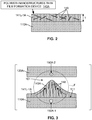
- Figs. 2 and 3 illustrate an unique attribute of the modified EHD patterning approach of the present invention in which "loaded" polymer thin films contain nanostructures that are inherently aligned during the formation of micro-scale polymer structures, thereby facilitating the production of a wide variety of highly valuable commercial applications.
- Fig. 2 is a partial cross-sectional view showing a liquid polymer thin film portion 141L-1A including nanostructures 148 (e.g., carbon nanotubes or GaAs nanowires).
- a polymer/nanostructure thin film formation device 140A e.g., one of coating systems mentioned above that is optimized to deposit the modified polymer/nanostructure material
- nanostructures 148 are dispersed with initial (e.g., random or non-random) orientations within liquid polymer thin film portion 141L-1A at deposition.
- Fig. 3 shows liquid polymer thin film portion 141L-1A when it is disposed in gap region 101 between lower conveyor 110 and upper conveyor 120 in a manner similar to that described above with reference to Fig. 1 .
- electric field F generated by voltage sources 150A-1 and 150A-2 causes EHD patterning deformation, whereby liquid polymer material flows inward and upward (as indicated by the dashed-line arrows) to form a patterned liquid polymer feature 143 that extends from liquid polymer thin film portion 141L-1A toward upper conveyor 120.
- nanostructures 148 when nanostructures 148 are reactive to an electric field (e.g., carbon nanotubes), nanostructures 148 align in electrical field F and couple to the hydrodynamic forces that result from the pattern formation, producing a generally vertical orientation (i.e., generally perpendicular to surface 111 of lower conveyor 110).
- an electric field e.g., carbon nanotubes
- Figs. 4(A) to 4(E) are simplified cross-sectional views illustrating system 100B according to an alternative embodiment of the present invention that produces separated (discrete) micro-scale structures for the creation of particles with increased specificity in the delivery of drugs.
- Fig. 4(A) depicts a polymer thin film portion 141B1(t0) at an initial time period (t0) on surface 111B of lower conveyor 110B.
- polymer thin film portion 141B1(t0) is formed by a slot coater or other thin film formation device 140B (not shown) while surface 111B is separated from surface 121B of upper conveyor 120B by relatively large distance D1.
- the polymer material forming polymer thin film portion 141B1(t0) has a relatively low viscosity and/or a thickness T1 of polymer thin film portion 141B1(t0) is intentionally lower than that used in the embodiments described above.
- Fig. 4(B) illustrates polymer thin film portion 141B1(t1) at a time period (t1) subsequent to time t0 after being moved by lower conveyor 110B into a position immediately upstream from the gap region, where surface 111B is separated from surface 121B by a relatively small distance D11.
- the applied electric field F(t1) generated by supplies 150B-1 and 150B-2 begins to cause EHD patterning of polymer thin film portion 141B1(t1), whereby the inward and upward flow of liquid polymer generates a liquid micro-scale patterned feature 143B(t1).
- Fig. 4(C) illustrates polymer thin film portion 141B1(t2) at a time period (t2) subsequent to time t1, when patterned feature 143B1(t2) is disposed in gap region 101B (i.e., where minimal gap distance G separates conveyors 110B and 120B). Due to the low viscosity and/or thin film thickness of the polymer thin film, the strength of electric field F(t2) causes patterned liquid polymer features 143B(t2) to separate from adjacent polymer features (not shown) on first surface 111B.
- patterned feature 143B1(t2) breaks away from adjacent features, whereby the liquid forming patterned feature 143B1(t2) comprises a discrete "island" of liquid polymer.
- the spacing and thickness of the polymer film are controlled such that the volume of liquid polymer drawn into each patterned feature (discrete liquid island) 143B1(t2) as it grows in the vertical (Z) direction (i.e., perpendicular to surface 111B) is equal to the volume of fluid in the negative space of the pattern, the EHD patterning process creates small particles of the same size scale as the patterns.
- Fig. 4(D) illustrates polymer thin film portion 141B1(t3) at a time period (t3) immediately subsequent to time t2, when patterned feature 143B1(t3) is disposed immediately downstream from the gap region (i.e., where conveyors 110B and 120B are separated by a distance D21 that is substantially equal to or slightly larger than the minimum gap distance).
- patterned feature 143B1(t3) a curing energy 161B (e.g., UV laser light) "freezes” (solidifies) discrete feature 143B1(t3) to form a solid micro-scale patterned particle (structure) 145B. Note that this curing process is performed on every discrete feature as it passes through the gap region, thereby generating multiple solid micro-scale patterned particles disposed in a spaced-apart arrangement on conveyor surface 111B.
- a curing energy 161B e.g., UV laser light
- Fig. 4(E) illustrates micro-scale patterned particle 145B subsequent to time period t3.
- a separator device 170B e.g., a knife edge
- Fig. 5 is a perspective view showing a system 100C according to a practical specific embodiment of the present invention in which the generalized conveyors mentioned above are implemented by parallel lower and upper rollers (conveyors) 110C and 120C, the generalized thin film formation device is implemented by a slot coater 140C, and the generalized curing device is implemented by a ultraviolet (UV) light source 160C, where these specific devices are controlled to perform a production method consistent with the generalized methods described above.
- the generalized conveyors mentioned above are implemented by parallel lower and upper rollers (conveyors) 110C and 120C
- the generalized thin film formation device is implemented by a slot coater 140C
- the generalized curing device is implemented by a ultraviolet (UV) light source 160C, where these specific devices are controlled to perform a production method consistent with the generalized methods described above.
- UV ultraviolet
- lower roller 110C is operably coupled to low voltage source 150C-1 such that it acts as the ground in the electric field circuit.
- the outer peripheral portions of lower roller 110C are made up of either an electrically conductive metal or an electrically conductive polymer, or outer surface 111C is optionally coated with an electrically conductive and/or transparent material such as ITO.
- Top roller 120C is operably coupled to high voltage source 150C-2 that supplies one or more high voltage signals to generate the applied electric field circuit.
- outer surface 121C of top roller 120C includes a continuous conductive layer that is electrically active across the entirety of roller surface 121C.
- top roller 120C includes either an electrode pattern or a dielectric material to which a charge pattern is applied.
- Lower roller 110C and upper roller 120C are driven by one or more motors 130C-1 and 130C-2 using techniques known in the art such that each region of surface 111C through nip-type gap region 101C substantially simultaneously with a corresponding region of surface 121C (i.e., rollers 110C and 120C are driven at matching speeds).
- Lower roller 110C and upper roller 120C are maintained by a support structure (also not shown) such that they remain separated by a fixed minimum distance G at a nip (gap) region 101C.
- a conventional high precision nip system 180C which is operably connected between the axis of rollers 110C and 120C to facilitate adjustment of minimum distance G using known techniques, serves to guarantees high roller distance dimensional control.
- Slot coater 140C coats (deposits) liquid polymer thin film 141C either directly onto cylinder roller surface 111C of lower roller 110C, or onto a support web (not shown) that is disposed over surface 111C. Slot coaters capable of performing this function are well known in the art. When polymer film 141C enters nip region 101C, it either replicates the pattern of electrodes disposed on upper roller 120C in the manner described below, or sets up a pattern based on the natural instability of the polymer system as described above.
- UV curable polymers are utilized because of their fast fixing time, and "fixing" mechanism is implemented by a system 160C (e.g., one of an Ultra Violet (UV) curing system, an visible light curing system, and a focused thermal curing system) that directs beam 161C onto a location adjacent to nip-type gap region 101C.
- system 160C e.g., one of an Ultra Violet (UV) curing system, an visible light curing system, and a focused thermal curing system
- beam 161C is applied such that the polymer is cross-linked and hardens into the solid micro-scale pattern shapes enforced on the liquid polymer by the applied electric field.
- UV laser systems capable of performing this curing function are well known in the art.
- the curing system is disposed inside one of rollers 110C and 120C, and is directed through transparent roller material into gap region 101C. Solidified polymer film (not shown) is then removed from lower roller 110C and moved downstream for any additional steps that might be required.
- roller width W is limited by the physical ability to both manufacture and install rollers 110C and 120C within the tolerances required. These tolerances are similar to those in typical slot coating systems, which can reasonably be expected to maintain a 0.5 micron tolerance over 3.5 meters. For one such realization of 8 micron features with a 2 micron tolerance, this leads to a maximum output of 1.3 m/s with fast UV cure times.
- the width can be increased and the sensitivity of the film pattern to machine tolerances can be adjusted for by varying the applied voltage through a number of electrode addressing schemes that are explained in further detail below.
- Fig. 6 is a simplified cross-sectional side view showing a system 100D according to another practical embodiment of the present invention.
- System 100D is characterized by a belt-to-belt arrangement formed by a lower belt-like conveyor 110D and an upper belt-like conveyor 120D that are positioned to define an elongated gap region 101D between opposing planar regions of lower belt surface 111D and upper belt surface 121D.
- a thin film deposition device e.g., a slot coater
- 140D is disposed to form a liquid polymer thin film 141D on lower belt surface 111D prior to entering gap region 101D, and voltage sources (not shown) are connected as described above to conductive material formed on the belts to generate the desired electric field inside elongated gap region 101D.
- the belt-to-belt arrangement of system 100D is similar to the roll-to-roll arrangement of 100C, but instead of a small nip-type gap area of the roll-to-roll arrangement, system 100D provides a large gap region that allows more time for the formation of the micro-scale pattern features.
- This arrangement facilitates the use of thermosetting polymers by facilitating thermal curing (e.g., by way of thermal curing systems (heater blocks) 160D disposed along the inside surface of the belt material adjacent to elongated gap region 101D).
- the belts are formed, for example, using a thermally conductive material, or a transparent material for admitting IR light into elongated gap region 101D.
- belt-like conveyors 110D and 120D must be held close by way of alignment blocks. This can either be achieved with significant amounts of tension or interlocking parts that slide in and out of the block using the arrangement indicated in Fig. 7 .
- Fig. 7 is a perspective cross-sectional view showing an interlocking arrangement according to a specific embodiment by which lower belt-like conveyor 110D is maintained in a precise planar orientation relative to an upper surface of underlying heater block (or other support structure) 160D.
- lower belt-like conveyor 110D includes a carrier belt portion 112D that slides over a planar upper surface 161D of heater block 160D such that patterned liquid features 143D form on conveyor surface 111D according to one of the processes described above.
- heater block 160D is constructed to define elongated T-shaped grooves 163D that extend in the moving direction X of lower belt-like conveyor 110D, and lower belt-like conveyor 110D includes T-shaped ribs 113D that extend below upper belt portion 112D and are slidably received in corresponding grooves 163D.
- Upper belt-like conveyor 120D ( Fig. 6 ) is constructed with a similar arrangement, thereby providing a sliding tongue-and-groove type arrangement that constrains the belts in the vertical direction and allows for tight tolerances to be achieved.
- Belt-to-belt system 100D facilitates higher production output speeds (i.e., linear belt speeds).
- the belt tolerances are largely dictated by the same tolerance limitations in the design of roll coating equipment. With precision machining it would be possible, in one possible realization to achieve a 0.5 micron tolerance over a 3.5 meter length. To create 8 micron features with a 2 micron tolerance over a 7 meter by 7 meter area, the total linear speed of the belts in this realization are limited to about 14 m/s. This realization is thus capable of much higher and industrially relevant throughput.
- belt-to-belt system 100D facilitates operations that do not require a curing device (i.e., system 100D).
- polymer 141D is heated and applied in a melted state onto surface 111D upstream of gap region 101D.
- the polymer temperature is high enough to maintain the melted state as the polymer is patterned by the applied electric field in the manner described above.
- the polymer is allowed to cool below the polymer's melting point temperature to form solid micro-scale patterned structures 145D having one of the forms described above.
- the various systems described above are modified to include digital patterning control, which is implemented using a dynamic charge generation mechanism that facilitates EHD patterning (i.e., electric field generation) by producing a dynamic (variable) charge pattern on at least one of the conveyor surfaces, whereby the charge pattern defining the electric field is dynamically alterable to compensate for system variances.
- EHD patterning i.e., electric field generation
- dynamic charge generation is achieved using either segmented electrodes or a charge patterning scheme.
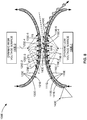
- Fig.8(A) is a simplified diagram depicting a system 100E includes a lower (first) conveyor 110E and an upper (second) conveyor 120E that are constructed and arranged to convey a polymer thin film 141E through a gap region 101E, where thin film 141E is generated on lower conveyor surface 111E by a suitable device 150E and patterned by an electric field F to form features 143E that are subsequently cured (e.g., by way of UV light 161E) to form micro-scale structures 145E in a manner similar to that described above.
- a suitable device 150E and patterned by an electric field F to form features 143E that are subsequently cured (e.g., by way of UV light 161E) to form micro-scale structures 145E in a manner similar to that described above.
- System 100E is characterized in that at least one of conveyors 110E and 120E includes segmented electrodes that are digitally addressable by a dynamic voltage source (electric field generator) such that each individual electrode receives an associated charge (voltage) having a value determined, e.g., by experimental measurement performed prior to production operations.
- upper conveyor 120E includes segmented upper electrodes 125E that are individually addressable by dynamic high voltage source (electric field generator) 150E-2 such that each individual upper electrode (e.g., electrodes 125E-1 to 125E-5) receives an associated (e.g., unique/different or common/same) voltage value.
- lower conveyor 110E includes segmented lower electrodes 115E that are digitally addressable by dynamic low voltage source (electric field generator) 150E-2 such that each individual lower electrode (e.g., electrodes 115E-1 to 115E-5) receives an associated voltage value.
- Sources 150E-1 and 150E-2 are electronic circuits produced in accordance with known techniques to generate and deliver associated voltage values such that each segmented electrode (or each upper/lower electrode pair) produces an associated portion of electric field F having an associated field strength.
- upper electrode 125E-1 (or the pair formed by upper electrode 125E-1 and lower electrode 115E-1) generate electric field portion F1 in the region between conveyor 110E and 120E.
- electrodes 125E-2 to 125E-5 (or pairs 125E-2/115E-2, 125E-3/115E-3, 125E-4/115E-4 and 125E-5/115E-5) generate electric field portions F2 to F5, respectively.
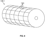
- Fig. 9 is a perspective view showing a roller-type upper conveyor 120E-1, which represents one type upper conveyor 120E used in system 100E (i.e., conveyor 120E may also be implemented using a belt-type conveyor).
- segmented upper electrodes 125E are arranged both along the rotational (circumferential) direction (i.e., as indicated in Fig. 8 ), and are also arranged along the cylindrical axis. That is, although the description related to Fig. 8 refers to variable charge patterns occurring along the rotational direction of roller-type conveyor 120E-1, it is understood that variable charge patterns discussed herein vary along the circumferential axis direction as well. That is, all electrodes 125E of roller-type upper conveyor 120E-1 are independently addressable such that each electrode receives an associated charge value.
- segmented electrodes 125E allow digital control over the electric field generated in gap region 101E during EHD patterning by facilitating the transmission of predetermined unique (different) or identical voltage values to each electrode, thereby allowing electrical correction (if needed) for physical variances that inevitably arise in large systems requiring precise tolerances, such as system 100E. That is, differences in localized electric field values F1 to F5, which may be caused by electrode distance variations between neighboring electrodes 125E-1 to 125E-5 or between paired electrodes (e.g., electrodes 115E-1 and 125E-1) across gap region 101E, are correctable by transmitting a predetermined unique "high" voltage to each electrode 125E-1 to 125E-5.
- each electrode 125E-1 to 125E-5 is individually addressed by dynamic high voltage source 150E-2 and receives an associated voltage whose value is set such that each electric field portion F1 to F5 has uniform field strength.
- the electrodes 125E arranged in the cylindrical axis direction i.e., as shown in Fig. 9
- dynamic high voltage source 150E-2 receives an associated voltage whose value is set such that each associated electric field portion also has a uniform field strength.
- Exemplary segmented electrodes with individual addressing schemes suitable for implementing electrodes 115E and 125E are disclosed in co-owned U.S. Patent No. 7,163,611 , entitled CONCENTRATION AND FOCUSING OF BIO-AGENTS AND MICRON-SIZED PARTICLES USING TRAVELING WAVE GRIDS, which is incorporated herein by reference in its entirety.
- segmented electrodes 125E have a modified (different) shape (e.g., line or point electrodes) that cover different parts of the "counter" surface depending on the patterns needed.
- a modified (different) shape e.g., line or point electrodes
- line or point electrodes Possible examples of line or point electrodes are disclosed in U.S. Patent No. 7,163,611 (cited above).
- Other electrode shapes e.g., hexagonal or circular are also possible, e.g., for making custom-shaped micro-scale particles.
- the size and distances between electrodes is altered to produce the desired EHD pattern.
- Fig. 8 indicates that each electrode pair produces a single separate micro-scale structure 145E, in other embodiments each electrode may be sized to generate multiple features/structures.
- a competing length scale to the intrinsic ⁇ max is introduced, which can either dominate the pattern formation dimension on the 2D plane, or define the area for the intrinsic pillar pattern.
- the voltages (charges) transmitted to each segmented electrode is changed (i.e., increased or decreased) over time, allowing for either custom pattern growth and or compensation of fabrication variations across the patterning area.
- These voltages can be adjusted dynamically, to either achieve specific quality metrics in the film, or to adjust as processing conditions change leading to an extremely robust process.
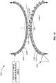
- Fig. 10 is a simplified diagram depicting another system 100F including a lower (first) conveyor 110F and an upper (second) conveyor 120F that are constructed and arranged to convey a polymer thin film 141F through a gap region 101F, where thin film 141F is deposited by device 140F and patterned by an electric field F to form features 143F that are subsequently cured to form micro-scale structures 145F in a manner similar to that described above.
- System 100F differs from the previous embodiment in that dynamic charge generation is achieved using well-defined charge patterns that are formed on an appropriate insulating or semiconducting material layer 123F disposed on surface 121F of upper conveyor 120F.
- first (e.g., positive) charges are selectively applied in a predetermined pattern on layer 123F by a first (e.g., positive) charge generating device 150F (e.g., a plasma generating device such as a scorotron) upstream of gap region 101F, whereby the first charges generate corresponding portions of electric field F in a manner similar to that described above with reference to the segmented electrode approach.
- a first (e.g., positive) charge generating device 150F e.g., a plasma generating device such as a scorotron
- relatively high charges are applied to the electrodes on lower conveyor 110F
- relatively low charges are applied to the electrodes of upper conveyor 120F.
- the charge patterns are achieved by either a masking process, or by a set of plasma generating devices of the required size.
- a photo sensitive material such as a photo receptor film similar to that used in a laser printer, is disposed on the upper conveyor, and the charge pattern is generated by light transmitted onto the photo sensitive material, where laser beam(s) are used to write a charge pattern on a photo receptor.
- the charge patterning approach provides an advantage in applications where different EHD patterns are needed in subsequent fabrication steps, or in continuous patterning systems (i.e. where each sheet or section of thin film has a different pattern).
- the charge patterning approach gives the biggest variability on the addressing electrodes, since the charge pattern can be changed easily from one step to the next, especially for the case of optical charge generation (similar to Xerography).
Landscapes
- Physics & Mathematics (AREA)
- General Physics & Mathematics (AREA)
- Application Of Or Painting With Fluid Materials (AREA)
- Micromachines (AREA)
- Shaping Of Tube Ends By Bending Or Straightening (AREA)
Applications Claiming Priority (1)
| Application Number | Priority Date | Filing Date | Title |
|---|---|---|---|
| US13/944,843 US9348231B2 (en) | 2013-07-17 | 2013-07-17 | Continuously producing digital micro-scale patterns on a thin polymer film |
Publications (2)
| Publication Number | Publication Date |
|---|---|
| EP2827192A1 EP2827192A1 (en) | 2015-01-21 |
| EP2827192B1 true EP2827192B1 (en) | 2019-02-27 |
Family
ID=51211592
Family Applications (1)
| Application Number | Title | Priority Date | Filing Date |
|---|---|---|---|
| EP14177409.1A Not-in-force EP2827192B1 (en) | 2013-07-17 | 2014-07-17 | Continuously producing digital micro-scale patterns on a thin polymer film |
Country Status (6)
| Country | Link |
|---|---|
| US (1) | US9348231B2 (enExample) |
| EP (1) | EP2827192B1 (enExample) |
| JP (1) | JP6293589B2 (enExample) |
| KR (1) | KR102093603B1 (enExample) |
| CN (1) | CN104290317B (enExample) |
| TW (1) | TWI631424B (enExample) |
Families Citing this family (13)
| Publication number | Priority date | Publication date | Assignee | Title |
|---|---|---|---|---|
| JP6037914B2 (ja) * | 2013-03-29 | 2016-12-07 | 富士フイルム株式会社 | 保護膜のエッチング方法およびテンプレートの製造方法 |
| US9884437B2 (en) | 2014-06-20 | 2018-02-06 | Palo Alto Research Center Incorporated | Integral vasculature |
| EP2974813A1 (de) * | 2014-07-17 | 2016-01-20 | MTU Aero Engines GmbH | Anlage und verfahren zur generativen herstellung und/oder reparatur von bauteilen |
| US10384432B2 (en) | 2016-02-19 | 2019-08-20 | Palo Alto Research Center Incorporated | Hierarchical laminates fabricated from micro-scale, digitally patterned films |
| WO2018052895A2 (en) * | 2016-09-16 | 2018-03-22 | 3M Innovative Properties Company | Method of making a nanostructured cylindrical roll |
| US10710283B2 (en) | 2016-12-22 | 2020-07-14 | Palo Alto Research Center Incorporated | Membrane surface hydrophobicity through electro-hydrodynamic film patterning |
| GB201701182D0 (en) * | 2017-01-24 | 2017-03-08 | Univ Birmingham | Surface enhanced raman scattering apparatus and method |
| NO342507B1 (en) * | 2017-03-29 | 2018-06-04 | Condalign As | A method for forming av body comprising at least one through-going passage |
| EP3671342B1 (en) * | 2018-12-20 | 2021-03-17 | IMEC vzw | Induced stress for euv pellicle tensioning |
| US11732378B2 (en) * | 2019-10-02 | 2023-08-22 | Palo Alto Research Center Incorporated | Three dielectric electrohydrodynamic patterning |
| CN112644158B (zh) * | 2020-06-28 | 2023-02-28 | 正扬科技有限公司 | 连续式紫外光固化装置 |
| CN112895408B (zh) * | 2020-12-28 | 2022-05-20 | 杭州电子科技大学 | 基于相场模型的聚合物表面微结构可控成形机理研究方法 |
| US20240012330A1 (en) * | 2021-02-21 | 2024-01-11 | The Regents Of The University Of California | Roll-to-roll based 3d printing through computed axial lithography |
Family Cites Families (19)
| Publication number | Priority date | Publication date | Assignee | Title |
|---|---|---|---|---|
| US2476282A (en) * | 1945-01-09 | 1949-07-19 | American Viscose Corp | Textile products and production thereof |
| US4166089A (en) * | 1969-11-13 | 1979-08-28 | Agfa-Gevaert N.V. | Corona free pinning of extruded polymer film |
| US6391217B2 (en) * | 1999-12-23 | 2002-05-21 | University Of Massachusetts | Methods and apparatus for forming submicron patterns on films |
| US6964793B2 (en) * | 2002-05-16 | 2005-11-15 | Board Of Regents, The University Of Texas System | Method for fabricating nanoscale patterns in light curable compositions using an electric field |
| KR20050025545A (ko) * | 2001-05-16 | 2005-03-14 | 보드 오브 리전츠, 더 유니버시티 오브 텍사스 시스템 | 전기장을 사용하여 광 중합 화합물내에 나노스케일의패턴을 생성하기 위한 방법 및 시스템 |
| JP2003343964A (ja) * | 2002-05-29 | 2003-12-03 | Glocal:Kk | 冷凍装置 |
| US6908861B2 (en) * | 2002-07-11 | 2005-06-21 | Molecular Imprints, Inc. | Method for imprint lithography using an electric field |
| MY144124A (en) * | 2002-07-11 | 2011-08-15 | Molecular Imprints Inc | Step and repeat imprint lithography systems |
| ITTO20020772A1 (it) * | 2002-09-06 | 2004-03-07 | Fiat Ricerche | Metodo per la realizzazione di strutture tridimensionali |
| JP2006506474A (ja) * | 2002-10-11 | 2006-02-23 | イー・アイ・デュポン・ドウ・ヌムール・アンド・カンパニー | パターニングされたフィブリル表面を有するフィルム、ならびにフィルムを製造するための方法および装置 |
| US7163611B2 (en) | 2003-12-03 | 2007-01-16 | Palo Alto Research Center Incorporated | Concentration and focusing of bio-agents and micron-sized particles using traveling wave grids |
| TWI345804B (en) * | 2005-08-17 | 2011-07-21 | Lg Chemical Ltd | Patterning method using coatings containing ionic components |
| KR100789581B1 (ko) | 2005-08-17 | 2007-12-28 | 주식회사 엘지화학 | 이온 성분을 함유하는 코팅액을 이용한 패턴 형성 방법 |
| JP2007062095A (ja) | 2005-08-30 | 2007-03-15 | Ricoh Co Ltd | プラスチック成形品の製造方法、及びその製造装置 |
| KR101265321B1 (ko) | 2005-11-14 | 2013-05-20 | 엘지디스플레이 주식회사 | 스탬프 제조 방법, 그를 이용한 박막트랜지스터 및액정표시장치의 제조 방법 |
| KR20090108853A (ko) * | 2008-04-14 | 2009-10-19 | 삼성전자주식회사 | 무기물 패턴 형성용 조성물 및 그를 이용한 무기물패턴형성 방법 |
| JP5542313B2 (ja) * | 2008-06-18 | 2014-07-09 | 協立化学産業株式会社 | パターン形成方法 |
| JP5129665B2 (ja) * | 2008-06-25 | 2013-01-30 | パナソニック株式会社 | プラズマ処理装置 |
| CN101620348B (zh) | 2008-07-04 | 2011-07-27 | 清华大学 | 触摸式液晶显示屏的制备方法 |
-
2013
- 2013-07-17 US US13/944,843 patent/US9348231B2/en not_active Expired - Fee Related
-
2014
- 2014-06-26 CN CN201410298767.7A patent/CN104290317B/zh not_active Expired - Fee Related
- 2014-06-27 JP JP2014133380A patent/JP6293589B2/ja not_active Expired - Fee Related
- 2014-07-04 KR KR1020140083679A patent/KR102093603B1/ko not_active Expired - Fee Related
- 2014-07-15 TW TW103124243A patent/TWI631424B/zh not_active IP Right Cessation
- 2014-07-17 EP EP14177409.1A patent/EP2827192B1/en not_active Not-in-force
Non-Patent Citations (1)
| Title |
|---|
| None * |
Also Published As
| Publication number | Publication date |
|---|---|
| KR102093603B1 (ko) | 2020-04-16 |
| EP2827192A1 (en) | 2015-01-21 |
| JP2015020434A (ja) | 2015-02-02 |
| US20150022790A1 (en) | 2015-01-22 |
| JP6293589B2 (ja) | 2018-03-14 |
| KR20150009923A (ko) | 2015-01-27 |
| CN104290317A (zh) | 2015-01-21 |
| US9348231B2 (en) | 2016-05-24 |
| TW201518868A (zh) | 2015-05-16 |
| CN104290317B (zh) | 2018-06-05 |
| TWI631424B (zh) | 2018-08-01 |
Similar Documents
| Publication | Publication Date | Title |
|---|---|---|
| EP2827192B1 (en) | Continuously producing digital micro-scale patterns on a thin polymer film | |
| EP2827193B1 (en) | Continuously producing digital micro-scale patterns on a thin polymer film | |
| US9651862B2 (en) | Drop pattern generation for imprint lithography with directionally-patterned templates | |
| Lu et al. | A Self‐Assembly Approach to the Fabrication of Patterned, Two‐Dimensional Arrays of Microlenses of Organic Polymers | |
| US9039402B2 (en) | Imprinting apparatus and method therefor | |
| CN101932754A (zh) | 单相流体印刻平板印刷方法 | |
| JP2015020435A5 (enExample) | ||
| Im et al. | Drop-on-demand electrohydrodynamic jet printing of microlens array on flexible substrates | |
| JP6486594B2 (ja) | 光学アレイを使用して微細構造を形成するためのフローリソグラフィ技法 | |
| US10744686B2 (en) | System for creating a structure including a vasculature network | |
| Shin et al. | Three-dimensional nanoprinting with charged aerosol focusing via an electrified mask | |
| JP2005525230A (ja) | 粒子の二次元集成のための方法及び装置 | |
| Park et al. | Rapid electrohydrodynamic-driven pattern replication over a large area via ultrahigh voltage pulses | |
| Jeong et al. | Spontaneous additive nanopatterning from solution route using selective wetting | |
| Zhang et al. | Patterned nanoparticle arrays fabricated using liquid film rupture self-assembly | |
| Zhong et al. | Roll-to-roll large-format slot die coating of photosensitive resin for UV embossing | |
| Chen et al. | Fabrication of sub-diffraction limit high-aspect-ratio nanostructures via laser direct writing | |
| Li et al. | Fabrication of micro-optical elements on curved substrates by electrostatic induced lithography | |
| Kim et al. | Characterization of 3D electrospinning on inkjet printed conductive pattern on paper | |
| Li et al. | Flexible Patterned Electrohydrodynamic Jet Printing Using Orthogonal Deflection Electrodes | |
| Duan et al. | 3D Turing nanowrinkles via anisotropic photopolymerization | |
| Li et al. | Formation of arbitrary patterns in ultraviolet cured polymer film via electrohydrodynamic patterning | |
| Li et al. | Influence of Template Geometry on Polymer Micro-Structure Duplication in Electrohydrodynamics Patterning Process |
Legal Events
| Date | Code | Title | Description |
|---|---|---|---|
| 17P | Request for examination filed |
Effective date: 20140717 |
|
| AK | Designated contracting states |
Kind code of ref document: A1 Designated state(s): AL AT BE BG CH CY CZ DE DK EE ES FI FR GB GR HR HU IE IS IT LI LT LU LV MC MK MT NL NO PL PT RO RS SE SI SK SM TR |
|
| AX | Request for extension of the european patent |
Extension state: BA ME |
|
| PUAI | Public reference made under article 153(3) epc to a published international application that has entered the european phase |
Free format text: ORIGINAL CODE: 0009012 |
|
| R17P | Request for examination filed (corrected) |
Effective date: 20150721 |
|
| RBV | Designated contracting states (corrected) |
Designated state(s): AL AT BE BG CH CY CZ DE DK EE ES FI FR GB GR HR HU IE IS IT LI LT LU LV MC MK MT NL NO PL PT RO RS SE SI SK SM TR |
|
| GRAP | Despatch of communication of intention to grant a patent |
Free format text: ORIGINAL CODE: EPIDOSNIGR1 |
|
| STAA | Information on the status of an ep patent application or granted ep patent |
Free format text: STATUS: GRANT OF PATENT IS INTENDED |
|
| INTG | Intention to grant announced |
Effective date: 20180926 |
|
| GRAS | Grant fee paid |
Free format text: ORIGINAL CODE: EPIDOSNIGR3 |
|
| GRAA | (expected) grant |
Free format text: ORIGINAL CODE: 0009210 |
|
| STAA | Information on the status of an ep patent application or granted ep patent |
Free format text: STATUS: THE PATENT HAS BEEN GRANTED |
|
| AK | Designated contracting states |
Kind code of ref document: B1 Designated state(s): AL AT BE BG CH CY CZ DE DK EE ES FI FR GB GR HR HU IE IS IT LI LT LU LV MC MK MT NL NO PL PT RO RS SE SI SK SM TR |
|
| REG | Reference to a national code |
Ref country code: GB Ref legal event code: FG4D |
|
| REG | Reference to a national code |
Ref country code: CH Ref legal event code: EP |
|
| REG | Reference to a national code |
Ref country code: DE Ref legal event code: R096 Ref document number: 602014041684 Country of ref document: DE |
|
| REG | Reference to a national code |
Ref country code: AT Ref legal event code: REF Ref document number: 1102246 Country of ref document: AT Kind code of ref document: T Effective date: 20190315 |
|
| REG | Reference to a national code |
Ref country code: IE Ref legal event code: FG4D |
|
| REG | Reference to a national code |
Ref country code: NL Ref legal event code: MP Effective date: 20190227 |
|
| REG | Reference to a national code |
Ref country code: LT Ref legal event code: MG4D |
|
| PG25 | Lapsed in a contracting state [announced via postgrant information from national office to epo] |
Ref country code: PT Free format text: LAPSE BECAUSE OF FAILURE TO SUBMIT A TRANSLATION OF THE DESCRIPTION OR TO PAY THE FEE WITHIN THE PRESCRIBED TIME-LIMIT Effective date: 20190627 Ref country code: SE Free format text: LAPSE BECAUSE OF FAILURE TO SUBMIT A TRANSLATION OF THE DESCRIPTION OR TO PAY THE FEE WITHIN THE PRESCRIBED TIME-LIMIT Effective date: 20190227 Ref country code: LT Free format text: LAPSE BECAUSE OF FAILURE TO SUBMIT A TRANSLATION OF THE DESCRIPTION OR TO PAY THE FEE WITHIN THE PRESCRIBED TIME-LIMIT Effective date: 20190227 Ref country code: NO Free format text: LAPSE BECAUSE OF FAILURE TO SUBMIT A TRANSLATION OF THE DESCRIPTION OR TO PAY THE FEE WITHIN THE PRESCRIBED TIME-LIMIT Effective date: 20190527 Ref country code: FI Free format text: LAPSE BECAUSE OF FAILURE TO SUBMIT A TRANSLATION OF THE DESCRIPTION OR TO PAY THE FEE WITHIN THE PRESCRIBED TIME-LIMIT Effective date: 20190227 Ref country code: NL Free format text: LAPSE BECAUSE OF FAILURE TO SUBMIT A TRANSLATION OF THE DESCRIPTION OR TO PAY THE FEE WITHIN THE PRESCRIBED TIME-LIMIT Effective date: 20190227 |
|
| PG25 | Lapsed in a contracting state [announced via postgrant information from national office to epo] |
Ref country code: RS Free format text: LAPSE BECAUSE OF FAILURE TO SUBMIT A TRANSLATION OF THE DESCRIPTION OR TO PAY THE FEE WITHIN THE PRESCRIBED TIME-LIMIT Effective date: 20190227 Ref country code: BG Free format text: LAPSE BECAUSE OF FAILURE TO SUBMIT A TRANSLATION OF THE DESCRIPTION OR TO PAY THE FEE WITHIN THE PRESCRIBED TIME-LIMIT Effective date: 20190527 Ref country code: IS Free format text: LAPSE BECAUSE OF FAILURE TO SUBMIT A TRANSLATION OF THE DESCRIPTION OR TO PAY THE FEE WITHIN THE PRESCRIBED TIME-LIMIT Effective date: 20190627 Ref country code: LV Free format text: LAPSE BECAUSE OF FAILURE TO SUBMIT A TRANSLATION OF THE DESCRIPTION OR TO PAY THE FEE WITHIN THE PRESCRIBED TIME-LIMIT Effective date: 20190227 Ref country code: GR Free format text: LAPSE BECAUSE OF FAILURE TO SUBMIT A TRANSLATION OF THE DESCRIPTION OR TO PAY THE FEE WITHIN THE PRESCRIBED TIME-LIMIT Effective date: 20190528 Ref country code: HR Free format text: LAPSE BECAUSE OF FAILURE TO SUBMIT A TRANSLATION OF THE DESCRIPTION OR TO PAY THE FEE WITHIN THE PRESCRIBED TIME-LIMIT Effective date: 20190227 |
|
| REG | Reference to a national code |
Ref country code: AT Ref legal event code: MK05 Ref document number: 1102246 Country of ref document: AT Kind code of ref document: T Effective date: 20190227 |
|
| PG25 | Lapsed in a contracting state [announced via postgrant information from national office to epo] |
Ref country code: SK Free format text: LAPSE BECAUSE OF FAILURE TO SUBMIT A TRANSLATION OF THE DESCRIPTION OR TO PAY THE FEE WITHIN THE PRESCRIBED TIME-LIMIT Effective date: 20190227 Ref country code: IT Free format text: LAPSE BECAUSE OF FAILURE TO SUBMIT A TRANSLATION OF THE DESCRIPTION OR TO PAY THE FEE WITHIN THE PRESCRIBED TIME-LIMIT Effective date: 20190227 Ref country code: EE Free format text: LAPSE BECAUSE OF FAILURE TO SUBMIT A TRANSLATION OF THE DESCRIPTION OR TO PAY THE FEE WITHIN THE PRESCRIBED TIME-LIMIT Effective date: 20190227 Ref country code: DK Free format text: LAPSE BECAUSE OF FAILURE TO SUBMIT A TRANSLATION OF THE DESCRIPTION OR TO PAY THE FEE WITHIN THE PRESCRIBED TIME-LIMIT Effective date: 20190227 Ref country code: AL Free format text: LAPSE BECAUSE OF FAILURE TO SUBMIT A TRANSLATION OF THE DESCRIPTION OR TO PAY THE FEE WITHIN THE PRESCRIBED TIME-LIMIT Effective date: 20190227 Ref country code: ES Free format text: LAPSE BECAUSE OF FAILURE TO SUBMIT A TRANSLATION OF THE DESCRIPTION OR TO PAY THE FEE WITHIN THE PRESCRIBED TIME-LIMIT Effective date: 20190227 Ref country code: RO Free format text: LAPSE BECAUSE OF FAILURE TO SUBMIT A TRANSLATION OF THE DESCRIPTION OR TO PAY THE FEE WITHIN THE PRESCRIBED TIME-LIMIT Effective date: 20190227 Ref country code: CZ Free format text: LAPSE BECAUSE OF FAILURE TO SUBMIT A TRANSLATION OF THE DESCRIPTION OR TO PAY THE FEE WITHIN THE PRESCRIBED TIME-LIMIT Effective date: 20190227 |
|
| REG | Reference to a national code |
Ref country code: DE Ref legal event code: R097 Ref document number: 602014041684 Country of ref document: DE |
|
| PG25 | Lapsed in a contracting state [announced via postgrant information from national office to epo] |
Ref country code: SM Free format text: LAPSE BECAUSE OF FAILURE TO SUBMIT A TRANSLATION OF THE DESCRIPTION OR TO PAY THE FEE WITHIN THE PRESCRIBED TIME-LIMIT Effective date: 20190227 Ref country code: PL Free format text: LAPSE BECAUSE OF FAILURE TO SUBMIT A TRANSLATION OF THE DESCRIPTION OR TO PAY THE FEE WITHIN THE PRESCRIBED TIME-LIMIT Effective date: 20190227 |
|
| PG25 | Lapsed in a contracting state [announced via postgrant information from national office to epo] |
Ref country code: AT Free format text: LAPSE BECAUSE OF FAILURE TO SUBMIT A TRANSLATION OF THE DESCRIPTION OR TO PAY THE FEE WITHIN THE PRESCRIBED TIME-LIMIT Effective date: 20190227 |
|
| PLBE | No opposition filed within time limit |
Free format text: ORIGINAL CODE: 0009261 |
|
| STAA | Information on the status of an ep patent application or granted ep patent |
Free format text: STATUS: NO OPPOSITION FILED WITHIN TIME LIMIT |
|
| 26N | No opposition filed |
Effective date: 20191128 |
|
| PG25 | Lapsed in a contracting state [announced via postgrant information from national office to epo] |
Ref country code: MC Free format text: LAPSE BECAUSE OF FAILURE TO SUBMIT A TRANSLATION OF THE DESCRIPTION OR TO PAY THE FEE WITHIN THE PRESCRIBED TIME-LIMIT Effective date: 20190227 Ref country code: SI Free format text: LAPSE BECAUSE OF FAILURE TO SUBMIT A TRANSLATION OF THE DESCRIPTION OR TO PAY THE FEE WITHIN THE PRESCRIBED TIME-LIMIT Effective date: 20190227 |
|
| REG | Reference to a national code |
Ref country code: CH Ref legal event code: PL |
|
| PG25 | Lapsed in a contracting state [announced via postgrant information from national office to epo] |
Ref country code: TR Free format text: LAPSE BECAUSE OF FAILURE TO SUBMIT A TRANSLATION OF THE DESCRIPTION OR TO PAY THE FEE WITHIN THE PRESCRIBED TIME-LIMIT Effective date: 20190227 |
|
| REG | Reference to a national code |
Ref country code: BE Ref legal event code: MM Effective date: 20190731 |
|
| PG25 | Lapsed in a contracting state [announced via postgrant information from national office to epo] |
Ref country code: LU Free format text: LAPSE BECAUSE OF NON-PAYMENT OF DUE FEES Effective date: 20190717 Ref country code: CH Free format text: LAPSE BECAUSE OF NON-PAYMENT OF DUE FEES Effective date: 20190731 Ref country code: LI Free format text: LAPSE BECAUSE OF NON-PAYMENT OF DUE FEES Effective date: 20190731 Ref country code: BE Free format text: LAPSE BECAUSE OF NON-PAYMENT OF DUE FEES Effective date: 20190731 |
|
| PG25 | Lapsed in a contracting state [announced via postgrant information from national office to epo] |
Ref country code: IE Free format text: LAPSE BECAUSE OF NON-PAYMENT OF DUE FEES Effective date: 20190717 |
|
| PG25 | Lapsed in a contracting state [announced via postgrant information from national office to epo] |
Ref country code: CY Free format text: LAPSE BECAUSE OF FAILURE TO SUBMIT A TRANSLATION OF THE DESCRIPTION OR TO PAY THE FEE WITHIN THE PRESCRIBED TIME-LIMIT Effective date: 20190227 |
|
| PG25 | Lapsed in a contracting state [announced via postgrant information from national office to epo] |
Ref country code: MT Free format text: LAPSE BECAUSE OF FAILURE TO SUBMIT A TRANSLATION OF THE DESCRIPTION OR TO PAY THE FEE WITHIN THE PRESCRIBED TIME-LIMIT Effective date: 20190227 Ref country code: HU Free format text: LAPSE BECAUSE OF FAILURE TO SUBMIT A TRANSLATION OF THE DESCRIPTION OR TO PAY THE FEE WITHIN THE PRESCRIBED TIME-LIMIT; INVALID AB INITIO Effective date: 20140717 |
|
| PG25 | Lapsed in a contracting state [announced via postgrant information from national office to epo] |
Ref country code: MK Free format text: LAPSE BECAUSE OF FAILURE TO SUBMIT A TRANSLATION OF THE DESCRIPTION OR TO PAY THE FEE WITHIN THE PRESCRIBED TIME-LIMIT Effective date: 20190227 |
|
| PGFP | Annual fee paid to national office [announced via postgrant information from national office to epo] |
Ref country code: GB Payment date: 20220621 Year of fee payment: 9 |
|
| PGFP | Annual fee paid to national office [announced via postgrant information from national office to epo] |
Ref country code: FR Payment date: 20220622 Year of fee payment: 9 |
|
| PGFP | Annual fee paid to national office [announced via postgrant information from national office to epo] |
Ref country code: DE Payment date: 20220621 Year of fee payment: 9 |
|
| REG | Reference to a national code |
Ref country code: DE Ref legal event code: R119 Ref document number: 602014041684 Country of ref document: DE |
|
| GBPC | Gb: european patent ceased through non-payment of renewal fee |
Effective date: 20230717 |
|
| PG25 | Lapsed in a contracting state [announced via postgrant information from national office to epo] |
Ref country code: DE Free format text: LAPSE BECAUSE OF NON-PAYMENT OF DUE FEES Effective date: 20240201 Ref country code: GB Free format text: LAPSE BECAUSE OF NON-PAYMENT OF DUE FEES Effective date: 20230717 |
|
| PG25 | Lapsed in a contracting state [announced via postgrant information from national office to epo] |
Ref country code: FR Free format text: LAPSE BECAUSE OF NON-PAYMENT OF DUE FEES Effective date: 20230731 |