EP2823564B1 - Étage de réception et procédé de réception - Google Patents
Étage de réception et procédé de réception Download PDFInfo
- Publication number
- EP2823564B1 EP2823564B1 EP13708403.4A EP13708403A EP2823564B1 EP 2823564 B1 EP2823564 B1 EP 2823564B1 EP 13708403 A EP13708403 A EP 13708403A EP 2823564 B1 EP2823564 B1 EP 2823564B1
- Authority
- EP
- European Patent Office
- Prior art keywords
- receiving
- signal
- paths
- comparators
- stage
- Prior art date
- Legal status (The legal status is an assumption and is not a legal conclusion. Google has not performed a legal analysis and makes no representation as to the accuracy of the status listed.)
- Active
Links
- 238000000034 method Methods 0.000 title claims description 15
- 230000003321 amplification Effects 0.000 claims description 27
- 238000003199 nucleic acid amplification method Methods 0.000 claims description 27
- 238000012545 processing Methods 0.000 claims description 4
- 238000010079 rubber tapping Methods 0.000 claims description 4
- 230000002452 interceptive effect Effects 0.000 claims 2
- 238000012935 Averaging Methods 0.000 claims 1
- 238000010586 diagram Methods 0.000 description 9
- 239000011159 matrix material Substances 0.000 description 5
- 230000008901 benefit Effects 0.000 description 4
- 230000006872 improvement Effects 0.000 description 4
- 238000013459 approach Methods 0.000 description 3
- 238000001514 detection method Methods 0.000 description 3
- 230000036039 immunity Effects 0.000 description 3
- 238000006243 chemical reaction Methods 0.000 description 2
- 238000004891 communication Methods 0.000 description 2
- 230000008569 process Effects 0.000 description 2
- 108010076504 Protein Sorting Signals Proteins 0.000 description 1
- 230000005540 biological transmission Effects 0.000 description 1
- 230000000903 blocking effect Effects 0.000 description 1
- 230000001427 coherent effect Effects 0.000 description 1
- 230000000052 comparative effect Effects 0.000 description 1
- 239000002131 composite material Substances 0.000 description 1
- 230000007423 decrease Effects 0.000 description 1
- 230000001934 delay Effects 0.000 description 1
- 230000001419 dependent effect Effects 0.000 description 1
- 238000011156 evaluation Methods 0.000 description 1
- 238000012986 modification Methods 0.000 description 1
- 230000004048 modification Effects 0.000 description 1
- 230000004044 response Effects 0.000 description 1
- 230000035945 sensitivity Effects 0.000 description 1
- 230000005236 sound signal Effects 0.000 description 1
Images


Classifications
-
- H—ELECTRICITY
- H03—ELECTRONIC CIRCUITRY
- H03G—CONTROL OF AMPLIFICATION
- H03G3/00—Gain control in amplifiers or frequency changers
- H03G3/20—Automatic control
- H03G3/30—Automatic control in amplifiers having semiconductor devices
- H03G3/3052—Automatic control in amplifiers having semiconductor devices in bandpass amplifiers (H.F. or I.F.) or in frequency-changers used in a (super)heterodyne receiver
-
- H—ELECTRICITY
- H04—ELECTRIC COMMUNICATION TECHNIQUE
- H04L—TRANSMISSION OF DIGITAL INFORMATION, e.g. TELEGRAPHIC COMMUNICATION
- H04L25/00—Baseband systems
- H04L25/02—Details ; arrangements for supplying electrical power along data transmission lines
- H04L25/08—Modifications for reducing interference; Modifications for reducing effects due to line faults ; Receiver end arrangements for detecting or overcoming line faults
-
- H—ELECTRICITY
- H04—ELECTRIC COMMUNICATION TECHNIQUE
- H04L—TRANSMISSION OF DIGITAL INFORMATION, e.g. TELEGRAPHIC COMMUNICATION
- H04L27/00—Modulated-carrier systems
- H04L27/02—Amplitude-modulated carrier systems, e.g. using on-off keying; Single sideband or vestigial sideband modulation
- H04L27/06—Demodulator circuits; Receiver circuits
Definitions
- Embodiments of the present invention refer to a receiving stage for receiving a receive signal and to a method for receiving a receive signal.
- a receiving stage is typically included by a receiver, e.g. a communication receiver or radio receiver. All types of radio receivers have the purpose of converting the information carried by the radio waves to a useable form, e.g. an audio signal or a (digital) data signal. Such wireless receivers are typically coupled to an antenna for receiving the electromagnetic wave or the RF signal (radio frequency signal).
- a receiver e.g. a communication receiver or radio receiver.
- All types of radio receivers have the purpose of converting the information carried by the radio waves to a useable form, e.g. an audio signal or a (digital) data signal.
- Such wireless receivers are typically coupled to an antenna for receiving the electromagnetic wave or the RF signal (radio frequency signal).
- the receiver typically comprises a receiving stage and a mixing stage arranged between the receiving stage and the antenna.
- the mixer stage has the purpose of performing a downmixing of the RF signal and to output an IF signal (intermediate frequency signal) to the receiving stage.
- the receiving stage may comprise an amplifier for increasing the IF signal amplitude and a demodulator for recovering the desired information, for example a bit sequence, based on the IF signal.
- the amplifier is adjustable in order to provide different amplification gains so that a weak signal, sent by a transmitter having a long distance, is more strongly amplified when compared to a strong signal, sent by a transmitter having a small distance.
- a state of the art approach for adjusting the amplification gain is to provide a so called automatic gain control (AGC) which is configured to adapt the gain of the amplifier as long as the signal output by the amplifier is out of a predetermined signal strength.
- AGC automatic gain control
- the adjustment of the amplification gain by using the automatic gain control takes time. Therefore, it cannot be guaranteed that a short signal sequence (short data telegram) may be received especially in case of signal strength changes (strong to weak or vice versa). In other words, a short data telegram could be missed. Thus, a repeated transmission of the telegram is required.
- AGC automatic gain control
- the patent application GB 2148638 A reveals an analog to a digital converter comprising a plurality of converts arranged in parallel, wherein the converters are logarithmically graduated.
- the patent application EP 1804414 A1 shows a gain control method for the RF and IF amplification stages of a bursty data frame reception system.
- the method comprises a step for evaluating the received signal strength, the gain adjustment step of the RF amplification stage to be temporarily deferred until a frame structure symbol is received, during which the gain adjustment step of the IF amplification stage takes place simultaneously with that of the RF gain.
- the patent application EP 0448071 A2 shows an adjustment unit for electrical signals, especially for ZF signals of a radio receiver.
- the adjustment unit comprises a digitally controllable signal converter and an analog to digital converter.
- the patent application EP 1598945 shows a wireless receiver detecting signals received at two or more antennas, with each antenna coupled to an input receive chain.
- a switch is employed to couple selected input receive chains to one or more corresponding output receive chains.
- the patent application US 2010/0141389 A1 shows an RFID transponder including an automatic gain control stage for amplifying a radio frequency signal and for providing an amplified RF signal.
- the automatic gain control stage has a control signal indicating an increase of the amplitude of the signal and a demodulator coupled to receive the amplified RF signal for demodulating same.
- the patent application US 7,463,704 B1 shows a wireless local area network system having multiple antennas to improve signal detection and decoding.
- the wireless local area network receiver includes multiple amplifiers that can appropriately size an incoming signal and an automatic gain control unit to process the received incoming signals.
- the patent application US 6,560,299 B1 shows a diversity receiver which is coupled to a composite antenna having first and second antennas physically configured to provide one or more forms of diversity reception.
- the multiple channel diversity receiver includes first and second RF channels.
- the objective of the present invention is to provide a concept for a receiving stage having an improved receipt behavior.
- An embodiment of the present invention provides a receiving stage for receiving a receive signal, e.g. an IF signal.
- the receiving stage comprises M receiving paths, wherein each receiving path comprises a signal processor and K comparators.
- the signal processors of the M receiving paths are configured to generate, for each of the M receiving paths, an amplified version of the receive signal such that an amplification gain of the respective receiving path increases from a first of the M receiving paths to a last of the M receiving paths.
- the K comparators of the respective receiving paths are configured to compare the amplified receive signal of the respective receiving path with a respective threshold value.
- the threshold value increases from a first of the K comparators to a last of the K comparators.
- Teachings of the present invention are based on recognizing that the adjustment of the amplification gain may become needless when the evaluation of the receive signal is performed in parallel receiving paths, wherein in each receiving path a version of the same signal amplified according different amplification gains (e.g. by different amplifiers having different gain) is evaluated. Consequently a receive signal having a weak signal strength is processed in a receiving path having a high amplification gain, wherein a receive signal having a strong signal strength is processed in a further receiving path having a low amplification gain. Thus, receive signals having different signal strengths may be received without any delay caused by the gain control in a manner enabling immediate processing.
- the processing of the receive signal may include evaluating the amplified receive signal, so each receiving path comprises besides the signal processor (e.g. amplifier), K comparators which are configured to compare the receive signal with respective (different) threshold values in order to output a bit sequence.
- the signal processor e.g. amplifier
- K comparators which are configured to compare the receive signal with respective (different) threshold values in order to output a bit sequence.
- the receiving stage may have a high input dynamic range and a quick response to dynamic changes of the desired signal, wherein the risk of missing telegrams is reduced due to the time advantages.
- the higher input dynamic range improves the immunity against interference, while keeping the time advantage compared to state of the art AGCs.
- a receiving stage having a high input dynamic range is formed due to the combination of the plurality of receiving paths (M receiving paths) and the plurality of comparators, wherein the dynamic range depends on the number of receiving paths (M) and on the number of comparators (K) and thus on the product M x K. Therefore, the receiving stage may be described by an M x K matrix (e.g. a 4 x 3 matrix).
- This M x K matrix may have two different variations.
- the receiving paths are received in parallel.
- the different amplification gains for the K receiving paths are generated by using different amplifiers having different gains so that in each of the M paths a different amplification gain is used.
- the amplifiers of the M signal processors comprising the amplifiers may be arranged in series, wherein the M comparator arrangements comprising the K comparators may be arranged in parallel.
- the amplification gain is graded from signal processor to signal processor due to the fact that a receive signal may be amplified several times, with the exception of the receive signal amplified for the first receiving path.
- the respective gains of the respective amplifiers may be equal.
- each signal processor may comprise an amplifier and a demodulator arranged between the amplifier and the comparator arrangement.
- the demodulator may be configured to demodulate the IF signal, for example based on a power detection or an envelope detection.
- each of the K comparators may be coupled to a correlator configured to detect a bit sequence forwarded by the respective comparator.
- the plurality of M x K comparators or correlators may be coupled to a digital selector configured to select or process (e.g. by means of combinational logic) one or multiples of the M x K channels via which the bit sequence is received.
- Fig. 1 shows a receiving stage 10 comprising M receiving paths 12a, 12b and 12c (M branches), wherein each receiving path comprises a signal processor 14a, 14b and 14c and K comparators 16a, 16b, 16c and 16d (K subbranches).
- the M receiving paths 12a, 12b and 12c are coupled to each other, for example via a common node 13, at the input side in order to receive the same receive signal (IF signal), for example from a mixing stage.
- IF signal receive signal
- This receive signal is processed or amplified by each of the signal processors 14a, 14b and 14c and output to the respective comparator arrangement 16 of the respective receiving path 12a, 12b and 12c, each comparator arrangement 16 comprising a plurality of comparators 16a, 16b, 16c and 16d.
- the comparators 16a, 16b, 16c and 16d are configured to compare the amplified receive signal of the respective receiving path 12a, 12b or 12c with a respective threshold value.
- the comparator arrangements 16 of the M receiving paths 12a - 12c are typically equal, wherein the K comparators 16a, 16b, 16c and 16d within a respective receiving path 12a, 12b or 12c differ from each other with regard to their threshold values.
- the threshold values of the K comparators 16a, 16b, 16c and 16d are selected such that the threshold value increases from a first of the K comparators 16a to a last of the K comparators 16d.
- Each comparator 16a, 16b, 16c and 16d is configured to output a binary signal, e.g. a "1", if the amplified receive signal is above the respective threshold value, and a "0" if the amplified receive signal is below the respective threshold value.
- the comparator is configured to output a digital signal based on an analog signal on the condition that the amplified receive signal oscillates around the respective threshold value.
- this means that the amplified receive signal has an off-level (lower value, e.g. -80 dBV) and an on-level (higher value, e.g. -70 dBV).
- Fig. 1 may be applied to a ASK (amplitude shift key) modulated receive signal, resulting in high input dynamic range without the time requirements of an automatic gain control
- the embodiments of Fig. 2a and 2b will benefit the receivers interferer immunity if the desired receive signal is modulated with OOK modulation, which is more thoroughly explained in the following.
- the signal levels are added as power levels, as shown by the following table: Table 1 Desired signal level Interferer level Total effective level (effective IF signal for data) -70 dBV -70 dBV -67 dBV -70 dBV -80 dBV -69,6 dBV
- a conversion of the receive signal into a digital signal may be able if the off-level and interferer level, respectively, is below one of the respective threshold values of the K comparators 16a to 16d and if the effective IF signal is above a respective threshold value of the respective comparator 16a to 16d, at times where the desired receive signal comprises a logical high state.
- the signal processors 14a, 14b and 14c which typically comprise amplifiers, of the M receiving paths may differ from each other.
- the different amplifiers and signal processors 14a, 14b and 14c, respectively are configured to generate, for each of the M receiving paths 12a, 12b and 12c, an amplified version of the receive signal such that an amplification gain of the respective receiving path 12a, 12b or 12c increases from a first of the M receiving paths 12a to a last of the M receiving paths 12c.
- the IF level of the received receive signal Due to the combination of the M receiving paths 12a to 12c and the K comparators 16a to 16d effective comparator thresholds (referred to as the IF level of the received receive signal) are generated which increase from the first comparator 16a of the first receiving path 12a to the last comparator 16d of the last signal path 12c.
- the receive signal may be processed or evaluated by M x K comparators, using M x K (effective comparator) thresholds, in parallel. This mode of operation of the receiving stage 10 formed by an M x K matrix will be discussed below.
- the discussion is made based on exemplary values for the amplification gain of the three signal processors 14a, 14b and 14c and for the threshold values of the comparators 16a, 16b, 16c and 16d.
- the exemplary amplification gain of the three signal processors 14a, 14b and 14c are 20 dB (14a), 30 dB (14b) and 40 dB (14c), wherein the exemplary threshold values of the four comparators 16a, 16b, 16c and 16d are -21 dBV (16a), -24 dBV (16b), - 27 dBV (16c) and -30 dBV (16d).
- the table 3 comprises for different receiving scenarios values for a data signal, for a continuous wave interferer signal and the resulting effective IF signal. Furthermore, the table comprises for each of the M x K comparators of the receiving stage 10 a respective output value for each receiving scenario.
- "0" means that the effective IF signal in the given scenario is below the effective comparator threshold at all (relevant) times, and wherein "1” means that effective IF signal is above the respective comparator thresholds at all (relevant) times.
- the table comprises a further column illustrating the comparator output of a simple OOK (On-Off Keying) comparator according to the state of the art.
- the receiver 10 extends the required signal to interferer ratio by allowing higher interferer levels. The topology allows a continuous signal reception without delays from the automatic gain control.
- Fig. 2a shows a further implementation of the receiving stage 10' comprising the M receiving paths 12a, 12b, 12c, wherein the receiving paths 12a, 12b and 12c are arranged in parallel to each other so that each of the signal processors 14a, 14b and 14c are directly coupled to the common node 13.
- Each receiving path 12a, 12b and 12c comprises the respective signal processor 14a, 14b and 14c and the comparator arrangement 16, wherein the comparator paths 16a, 16b, 16c and 16d are arranged in parallel and coupled to further respective common nodes 15a, 15b and 15c.
- Each of the signal processors 14a, 14b and 14c is formed by a combination of an amplifier 24a, 24b and 24c with a demodulator 26a, 26b and 26c.
- the amplifiers 24a, 24b and 24c have different gains in order to provide different amplification gains at the output of the signal processor 14a, 14b and 14c. Consequently, the receive signal is amplified differently.
- the amplified receive signal may, for example, be an amplitude modulated signal or another alternating signal which has to be demodulated before provided to the comparator paths 16a, 16b, 16c and 16d.
- the demodulation is performed by respective demodulators 26a, 26b and 26c.
- the demodulators 26a, 26b and 26c may, for example, be formed by a peak detector, power detector or an envelope detector.
- the demodulators 26a, 26b and 26c may comprise another detector for demodulating an amplitude modulator signal or, in general, detector which is configured to an output a demodulated signal, like a DC voltage, to the comparator arrangements 16 based on an (alternating) receive signal.
- All of the M x K comparators 16a, 16b, 16c, 16d of the receiving paths 12a, 12b and 12c are coupled to a digital selector 20.
- the digital selector 20 may be formed by an OR-operation unit.
- the digital selector 20 has the purpose of selecting or processing one or more of M x K channels and to forward the information to the output of the selector.
- each comparator 16a to 16d of the M receiving paths 12a, 12b or 12c may optionally be coupled to the digital selector 20 via a correlator 22a, 22b, 22c and 22d (correlator arrangement 22).
- each correlator 22a to 22d indicates a certain code match due to the corresponding comparator data.
- the output at the digital selector 20 is shown, wherein 1 at the output at the digital selector 20 means code match achieved and 0 means no code match achieved. Comparing the simple OOK correlator output (using only one comparator and one correlator) with the e.g. ORed correlator output signals, a strong improvement can be observed. Seven signal scenarios can be met by the proposed architecture. In contrary, a simple OOK receiver with a single comparator and a single correlator only meets one of the scenarios. In other words the higher input dynamic range leads to substantial improvement of interferer immunity. It should be noted that it is useful to use spread sequence modulation IF signals to distinguish the modulated interferer and the data modulated signals in the correlator.
- Fig. 2b shows a further receiving stage 10" comprising the M receiving paths 12a, 12b and 12c, wherein each receiving path comprises the comparator arrangement 16 coupled via the correlators 22a, 22b, 22c and 22d to the digital selector 20.
- the M receiving paths 12a, 12b and 12c are not coupled to a common node, but partially coupled in series.
- the second receiving path 12b is coupled to the first receiving path 12a via a first tapping 28a at the output of the amplifier 24a of the first signal processor 14a, i.e. that the tapping 28a is arranged between the amplifier 24a and the optional demodulator 26a.
- the signal processor 14c of the last receiving path 12c is coupled to the output of the amplifier 24b of the previous receiving path 12b via a tapping 28b.
- the signal amplified by the second amplifier 24b of the second receiving path 12b is pre-amplified by the first amplifier 24a of the first receiving path 12a, wherein the signal amplified by the amplifier 24c is pre-amplified by the amplifiers 24b and 24a of the previous receiving paths 12a and 12b. Consequently, the amplification gains increase from the first receiving path 12a to the last receiving path 12c, although the gains of the amplifiers 24a, 24b and 24c may be equal or may be selected arbitrarily.
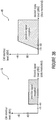
- Fig. 3a shows a reception map 40 illustrating the signal strength for a receiver 44 comprising one of the receiving stages 10, 10' or 10", wherein the TX signal is disturbed by an interferer 42.
- the emitted power of the interferer 42 is 100 mW.
- the desired signal is emitted with 10 mW.
- the distance between the two signal sources is 300 m (cf. broken line).
- the desired circle arcs represent the equipower lines of the interferer 42 meaning that the power of the interferer signal equals an annotated value, for all points on the arc.
- the hatched area represents the location in which the signal level is larger than the interferer level in the given scenario.
- the signal to interferer ratio (CIR) is larger than 10 dB and decreases with increasing distance.
- the proposed architecture of the receiving stages 10, 10' or 10" allows reception with low signal to interferer ratio (e.g. 3 dB), when using OOK modulated data on the receive signal.
- a short data telegram would have to be repeated several times, until the feedback loop locks the IF signal onto proper reception/sensing level for a comparator. With the proposed method there is no delay due to gain adjust and no telegram is missed.
- Fig. 3b shows two diagrams 46 and 48 in which the possible signal reception is marked dependent on the CW signal level (CW interferer level) and the data signal level (desired signal level).
- the first diagram 46 illustrates the possible signal reception (hatched area) for a simple OOK correlating receiver (using one comparator and one correlator).
- the second diagram 48 illustrates the possible signal reception for a receiver (cf. 10, 10' and 10") having an extended dynamic range using multiple comparators and correlators.
- the comparison with the two diagrams 46 and 48 regarding the CW signal level shows that a receiver 10, 10' and 10" having the improved receiving stage is able to receive a signal up to a CW signal level which is higher when compared to the state of the art approach.
- the desired signal level may be smaller (cf. data signal level: - 70 dBV point) in case of low interference.
- receivers 10, 10' and 10" are explained as receivers having three receiving paths 12a, 12b and 12c with four comparators 16a, 16b, 16c and 16d, it should be noted that the number M of the receiving paths as well as the number K of the comparators may vary.
- the difference between two successive amplification gains of the plurality of receiving paths 12a, 12b and 12c are preferably equidistant.
- the difference between two successive amplification gains may be 10 of 15 dB.
- the threshold values have been discussed as pressure values which equal for each of the M comparator arrangements 16, it should be noted that the pressure values may, alternatively, vary from the first receiving path 12a to the last receiving paths 12c.
- the outputs of the M x K comparators may be used to perform an occupancy estimation of the RF channel.
- aspects have also been described in the context of an apparatus, it is clear that the aspects also represent a description of the corresponding method, where a block or a device corresponds to a method step or a feature of the method step. Analogously, aspects described in the context of the method step also represent the description of a corresponding block, item or feature of the corresponding apparatus.
- Some or all of the method steps may be executed by (or using) a hardware apparatus, like a microprocessor, programmable computer or an electronic circuit. In some embodiments, some one or more of the most important method steps may be executed by such an apparatus.
Landscapes
- Engineering & Computer Science (AREA)
- Computer Networks & Wireless Communication (AREA)
- Signal Processing (AREA)
- Power Engineering (AREA)
- Circuits Of Receivers In General (AREA)
- Dc Digital Transmission (AREA)
- Noise Elimination (AREA)
Claims (18)
- Etage de réception (10, 10', 10") destiné à recevoir un signal de réception, comprenant:M trajets de réception (12a, 12b, 12c), chaque trajet de réception (12a, 12b, 12c) comprenant un processeur de signal (14a, 14b, 14c) et K comparateurs (16a, 16b, 16c, 16d),dans lequel chacun des K comparateurs (16a, 16b, 16c, 16d) est couplé à une unité de corrélation (22a, 22b, 22c, 22d) configurée pour détecter une séquence de bits transmise par le comparateur respectif (16a, 16b, 16c, 16d),dans lequel les processeurs de signal (14a, 14b, 14c) des M trajets de réception (12a, 12b, 12c) sont configurés pour générer, pour chacun des M trajets de réception (12a, 12b, 12c), une version amplifiée du signal de réception de sorte qu'un gain d'amplification du trajet de réception respectif (12a, 12b, 12c) augmente d'un premier des M trajets de réception (12a, 12b, 12c) à un dernier des M trajets de réception (12a, 12b, 12c),dans lequel, pour chacun des M trajets de réception (12a, 12b, 12c), les K comparateurs (16a, 16b, 16c, 16d) des trajets de réception respectifs (12a, 12b, 12c) sont configurés pour comparer le signal de réception amplifié du trajet de réception respectif (12a, 12b, 12c) avec une valeur de seuil respective et, pour chacun des M trajets de réception (12a, 12b, 12c), la valeur de seuil augmente d'un premier des K comparateurs (16a, 16b, 16c, 16d) au dernier des K comparateurs (16a, 16b, 16c, 16d).
- Etage de réception (10, 10', 10") selon la revendication 1, dans lequel les M trajets de réception (12a, 12b, 12c) sont disposés en parallèle et couplés à un noeud commun (13) de son côté d'entrée.
- Etage de réception (10, 10', 10") selon la revendication 2, dans lequel les processeurs de signal respectifs (14a, 14b, 14c) des M trajets de réception (12a, 12b, 12c) présentent des gains différents.
- Etage de réception (10, 10', 10") selon l'une des revendications 1 à 3, dans lequel chaque processeur de signal (14a, 14b, 14c) des M trajets de réception (12a, 12b, 12c) comprend un amplificateur (24a, 24b, 24c).
- Etage de réception (10, 10', 10") selon la revendication 4, dans lequel chaque processeur de signal (14a, 14b, 14c) des M trajets de réception (12a, 12b, 12c) comprend un démodulateur (26a, 26b, 26c) disposé entre l'amplificateur respectif (24a, 24b, 24c) et les K comparateurs (16a, 16b, 16c, 16d).
- Etage de réception (10, 10', 10") selon l'une des revendications 1 à 5, dans lequel les processeurs de signal (14a, 14b, 14c) des M trajets de réception sont disposés en série et dans lequel les K comparateurs (16a, 16b, 16c, 16d) des M trajets de réception (12a, 12b, 12c) sont disposés en parallèle.
- Etage de réception (10, 10', 10") selon la revendication 6, dans lequel chaque processeur de signal (14a, 14b, 14c) des M trajets de réception (12a, 12b, 12c) comprend un amplificateur (24a, 24b, 24c) et dans lequel les gains des amplificateurs respectifs des M trajets de réception (12a, 12b, 12c) sont égaux, de sorte qu'au moins le gain d'amplification du dernier des M trajets de réception (12a, 12b, 12c) soit basé sur une combinaison du gain de l'amplificateur du premier des M trajets de réception (12a, 12b, 12c) et du gain de l'amplificateur du dernier des M trajets de réception (12a, 12b, 12c).
- Etage de réception (10, 10', 10") selon la revendication 7, dans lequel chaque processeur de signal (14a, 14b, 14c) des M trajets de réception (12a, 12b, 12c) comprend un amplificateur (24a, 24b, 24c) et un démodulateur (26a, 26b, 26c) disposé entre l'amplificateur (24a, 24b, 24c) et les K comparateurs (16a, 16b, 16c, 16d), dans lequel, pour chacun des M trajets de réception (12a, 12b, 12c), une dérivation pour le suivant des M trajets de réception (12a, 12b, 12c) est disposée entre l'amplificateur respectif (24a, 24b, 24c) et le démodulateur respectif (26a, 26b, 26c).
- Etage de réception (10, 10', 10") selon l'une des revendications 1 à 8, dans lequel les K comparateurs (16a, 16b, 16c, 16d) sont disposés en parallèle et couplés au processeur de signal respectif (14a, 14b, 14c) par l'intermédiaire d'un noeud commun (15a, 15b, 15c).
- Etage de réception (10, 10', 10") selon l'une des revendications 1 à 9, dans lequel les K comparateurs (16a, 16b, 16c, 16d) sont configurés pour transmettre le signal de réception amplifié si le signal de réception amplifié est supérieur à une valeur de seuil respective et qu'une différence entre le signal de réception amplifié et un signal d'interférence est supérieure à une distance moyenne des K valeurs de seuil, dans lequel le signal de réception comprend le signal d'interférence et un signal de données portant la séquence de bits.
- Etage de réception (10, 10', 10") selon la revendication 10 ou 11, dans lequel le corrélateur respectif (22a, 22b, 22c, 22d) comprend une unité d'opérateur XNOR ou une unité d'opérateur XOR.
- Etage de réception (10, 10', 10") selon l'une des revendications 10 à 12, dans lequel chaque corrélateur (22a, 22b, 22c, 22d) de l'M trajet de réception (12a, 12b, 12c) est couplé à un sélecteur numérique (20) configuré pour sortir des informations sur base de la séquence de bits détectée par l'un des K corrélateurs (22a, 22b, 22c, 22d).
- Etage de réception (10, 10', 10") selon la revendication 12, dans lequel le sélecteur numérique (20) comprend une logique combinatoire pour la sélection et/ou le traitement d'un ou plusieurs des K x M canaux, chaque canal étant formé par le corrélateur respectif (22a, 22b, 22c, 22d) de 1'M trajet de réception (12a, 12b, 12c).
- Etage de réception (10, 10', 10") selon la revendication 12 ou 13, dans lequel le sélecteur numérique (20) est configuré pour sortir des informations sur le corrélateur respectif (22a, 22b, 22c, 22d) dans lequel est détectée la séquence de bits.
- Etage de réception (10, 10', 10") selon la revendication 5, dans lequel le démodulateur (26a, 26b, 26c) comprend un détecteur de crête, un détecteur de puissance, un détecteur d'enveloppe et/ou un détecteur pour démoduler un signal de modulateur d'amplitude.
- Etage de réception (10, 10', 10") selon l'une des revendications 1 à 15, dans lequel les M-1 différences entre deux gains d'amplification successifs des M gains d'amplification sont équidistantes.
- Etage de réception (10, 10', 10") selon la revendication 16, dans lequel une distance moyenne entre les K valeurs de seuil est au moins deux fois plus petite que la différence entre deux gains d'amplification successifs.
- Procédé permettant de recevoir un signal de réception, à l'aide de l'étage de réception (10, 10', 10") comprenant M trajets de réception (12a, 12b, 12c), chaque trajet de réception (12a, 12b, 12c) comprenant un processeur de signal (14a, 14b, 14c) et K comparateurs (16a, 16b, 16c, 16d), le procédé comprenant le fait de:générer une version amplifiée du signal de réception pour chacun des M trajets de réception (12a, 12b, 12c), à l'aide du processeur de signal respectif (14a, 14b, 14c) du trajet de réception moyen, de sorte qu'un gain d'amplification des trajets de réception respectifs (12a, 12b, 12c) augmente d'un premier du trajet moyen (12a, 12b, 12c) à un dernier des trajets de réception (12a, 12b, 12c); etcomparer le signal de réception amplifié des trajets de réception respectifs (12a, 12b, 12c) avec une valeur de seuil respective pour chacun des M trajets de réception, à l'aide des K comparateurs (16a, 16b, 16c, 16d) des trajets de réception respectifs (12a, 12b, 12c), dans lequel, pour chacun des trajets de réception (12a, 12b, 12c), la valeur de seuil augmente d'un premier des K comparateurs (16a, 16b, 16c, 16d) à un dernier des K comparateurs (16a, 16b, 16c, 16d),dans lequel chacun des K comparateurs (16a, 16b, 16c, 16d) est couplé à une unité de corrélation (22a, 22b, 22c, 22d) configurée pour détecter une séquence de bits transmise par le comparateur respectif (16a, 16b, 16c, 16d).
Applications Claiming Priority (2)
| Application Number | Priority Date | Filing Date | Title |
|---|---|---|---|
| US201261607320P | 2012-03-06 | 2012-03-06 | |
| PCT/EP2013/054523 WO2013131966A2 (fr) | 2012-03-06 | 2013-03-06 | Étage de réception et procédé de réception |
Publications (2)
| Publication Number | Publication Date |
|---|---|
| EP2823564A2 EP2823564A2 (fr) | 2015-01-14 |
| EP2823564B1 true EP2823564B1 (fr) | 2017-01-04 |
Family
ID=47844304
Family Applications (1)
| Application Number | Title | Priority Date | Filing Date |
|---|---|---|---|
| EP13708403.4A Active EP2823564B1 (fr) | 2012-03-06 | 2013-03-06 | Étage de réception et procédé de réception |
Country Status (4)
| Country | Link |
|---|---|
| US (1) | US9407228B2 (fr) |
| EP (1) | EP2823564B1 (fr) |
| JP (1) | JP5887433B2 (fr) |
| WO (1) | WO2013131966A2 (fr) |
Family Cites Families (37)
| Publication number | Priority date | Publication date | Assignee | Title |
|---|---|---|---|---|
| US3569953A (en) * | 1968-03-25 | 1971-03-09 | Sylvania Electric Prod | Wide range analogue to digital converter |
| DE3337041C1 (de) * | 1983-10-12 | 1985-04-18 | Krautkrämer GmbH, 5000 Köln | Schaltungsvorrichtung zur Logarithmierung und Digitalisierung analoger Signale |
| JPS61284125A (ja) * | 1985-06-11 | 1986-12-15 | Nec Corp | ダイバ−シチ受信方式 |
| JPH03213021A (ja) * | 1990-01-18 | 1991-09-18 | Fujitsu Ltd | Sd受信装置 |
| DE4009140C2 (de) * | 1990-03-21 | 1997-04-03 | Plath Naut Elektron Tech | Regeleinrichtung für Funkempfänger |
| US5742896A (en) * | 1990-11-09 | 1998-04-21 | Bose Corporation | Diversity reception with selector switching at superaudible rate |
| JP2643614B2 (ja) * | 1991-02-22 | 1997-08-20 | 日本電気株式会社 | ディジタル移動通信端末装置 |
| JPH0884104A (ja) * | 1994-09-09 | 1996-03-26 | Toshiba Corp | 無線通信装置 |
| JP3586004B2 (ja) * | 1995-08-22 | 2004-11-10 | 富士通株式会社 | 移動無線通信の誤り率検出装置 |
| FI100041B (fi) * | 1995-12-29 | 1997-08-29 | Nokia Telecommunications Oy | Menetelmä signaalin ja kohinan laadun estimoimiseksi ja vastaanotin |
| US6393046B1 (en) * | 1996-04-25 | 2002-05-21 | Sirf Technology, Inc. | Spread spectrum receiver with multi-bit correlator |
| JPH11220346A (ja) * | 1998-02-02 | 1999-08-10 | Fujitsu Ltd | 自動利得制御回路 |
| JP3362699B2 (ja) * | 1999-06-10 | 2003-01-07 | 日本電気株式会社 | 空間送受信ダイバーシチ通信システム |
| US6560299B1 (en) * | 1999-07-30 | 2003-05-06 | Christopher H Strolle | Diversity receiver with joint signal processing |
| US6191725B1 (en) * | 1999-08-30 | 2001-02-20 | Her Majesty The Queen In Right Of Canada, As Represented By Minister Of National Defence Of Her Majesty's Canadian Government | Automatic gain control for digital radar intercept receivers |
| JP3358603B2 (ja) * | 1999-11-04 | 2002-12-24 | 日本電気株式会社 | パスタイミング検出回路及びその検出方法 |
| JP4321959B2 (ja) * | 2000-10-17 | 2009-08-26 | Okiセミコンダクタ株式会社 | 信号補償回路及び復調回路 |
| US6963733B2 (en) * | 2001-10-31 | 2005-11-08 | Telefonaktiebolaget L M Ericsson (Publ) | Method and apparatus for reducing the effect of AGC switching transients |
| JP2004147082A (ja) * | 2002-10-24 | 2004-05-20 | Matsushita Electric Ind Co Ltd | 通信装置 |
| US7310503B2 (en) * | 2002-10-28 | 2007-12-18 | Mitsubishi Denki Kabushiki Kaisha | Diversity reception device and diversity reception method |
| JP2004297320A (ja) * | 2003-03-26 | 2004-10-21 | Alps Electric Co Ltd | ダイバーシティ受信装置 |
| JP3906179B2 (ja) * | 2003-04-25 | 2007-04-18 | 株式会社東芝 | 無線受信機および無線信号処理方法 |
| JP4229816B2 (ja) * | 2003-11-25 | 2009-02-25 | シャープ株式会社 | 受信装置 |
| DE102004011780A1 (de) * | 2004-03-09 | 2005-10-27 | Gerd Reime | Zugangskontrolleinrichtung |
| US7356322B2 (en) * | 2004-05-17 | 2008-04-08 | Agere Systems Inc. | Multiple-branch wireless receiver |
| US7463704B1 (en) * | 2004-07-01 | 2008-12-09 | Atheros Communications, Inc. | Multi-chain signal detection and gain control for automatic gain control systems |
| JP4682684B2 (ja) * | 2005-04-28 | 2011-05-11 | パナソニック株式会社 | デジタル信号受信装置 |
| US7787841B2 (en) * | 2005-06-13 | 2010-08-31 | Panasonic Corporation | Receiving module and receiving device using the same |
| US7953191B2 (en) * | 2005-12-28 | 2011-05-31 | Thomson Licensing | Gain control method and device for a bursty data frame reception system |
| TW200805919A (en) * | 2006-07-12 | 2008-01-16 | Matsushita Electric Ind Co Ltd | A diversity receiver and method using the same |
| JP2008271441A (ja) * | 2007-04-24 | 2008-11-06 | Sharp Corp | 信号分配装置、受信装置、及び当該受信装置を備える機器 |
| JP2009060178A (ja) * | 2007-08-29 | 2009-03-19 | Sharp Corp | ダイバーシティ装置 |
| US7853224B2 (en) * | 2007-11-02 | 2010-12-14 | Micrel, Incorporated | Fast settling radio receiver automatic gain control system |
| JP5074279B2 (ja) * | 2008-04-22 | 2012-11-14 | ルネサスエレクトロニクス株式会社 | 信号処理装置 |
| DE102008060082B4 (de) * | 2008-12-02 | 2019-09-05 | Texas Instruments Deutschland Gmbh | RFID-Transponder mit verbesserter Weckmusterdetektion und Verfahren |
| KR101554220B1 (ko) * | 2009-06-03 | 2015-09-21 | 삼성전자주식회사 | 휴대단말기의 근접 센서를 이용한 데이터 출력 방법 및 장치 |
| KR20100136649A (ko) * | 2009-06-19 | 2010-12-29 | 삼성전자주식회사 | 휴대단말기의 근접 센서를 이용한 사용자 인터페이스 구현 방법 및 장치 |
-
2013
- 2013-03-06 WO PCT/EP2013/054523 patent/WO2013131966A2/fr active Application Filing
- 2013-03-06 EP EP13708403.4A patent/EP2823564B1/fr active Active
- 2013-03-06 JP JP2014560355A patent/JP5887433B2/ja active Active
-
2014
- 2014-09-04 US US14/477,825 patent/US9407228B2/en active Active
Non-Patent Citations (1)
| Title |
|---|
| None * |
Also Published As
| Publication number | Publication date |
|---|---|
| WO2013131966A2 (fr) | 2013-09-12 |
| US20140376666A1 (en) | 2014-12-25 |
| WO2013131966A3 (fr) | 2013-10-31 |
| JP5887433B2 (ja) | 2016-03-16 |
| JP2015513263A (ja) | 2015-04-30 |
| EP2823564A2 (fr) | 2015-01-14 |
| US9407228B2 (en) | 2016-08-02 |
Similar Documents
| Publication | Publication Date | Title |
|---|---|---|
| CN107276621B (zh) | 兼顾多种应用场景的接收机自动增益控制系统及方法 | |
| JP5342099B2 (ja) | 測距・通信複合システム | |
| JP2001251242A5 (fr) | ||
| US10404497B2 (en) | Non-coherent multi-symbol-delay differential detector | |
| US8189715B2 (en) | Receiver for receiving data symbols having a symbol period | |
| EP2628340A1 (fr) | Système et procédé de retrait sélectif d'un canal dans des récepteurs multicanaux | |
| JP4631533B2 (ja) | 無線通信装置 | |
| US8724750B2 (en) | Adjacent channel rejection of a CCK blocker | |
| US8009718B2 (en) | Wireless transmitter and receiver for use in an ultra-wideband direct spread pulse communication system | |
| EP2823564B1 (fr) | Étage de réception et procédé de réception | |
| US8655295B2 (en) | Receiving apparatus | |
| US10594282B2 (en) | Automatic gain control (AGC) circuit, despreading circuit, and method for reproducing reception data | |
| US20160028450A1 (en) | Robust wireless communication system and components thereof for processing a message from two sources | |
| US9319102B2 (en) | Communication apparatus, communication system, communication method, and storage medium | |
| US10939468B2 (en) | Clear channel assessment | |
| JP6229518B2 (ja) | 無線受信装置及び無線受信方法 | |
| US10050666B2 (en) | Devices for detecting ultra-wide band signals | |
| KR101924906B1 (ko) | 이득 제어 장치 및 방법 | |
| JP4845819B2 (ja) | 信号検出装置、受信機およびしきい値算出方法 | |
| US9537518B2 (en) | Power sensing in wireless system | |
| EP3393050A1 (fr) | Récepteur sans fil | |
| EP0583966B1 (fr) | Commande automatique de gain | |
| JP5413962B2 (ja) | 無線通信システム | |
| JPH01311642A (ja) | ダイバーシチ受信方式 | |
| JP2023005139A (ja) | 信号処理回路及び電子機器 |
Legal Events
| Date | Code | Title | Description |
|---|---|---|---|
| PUAI | Public reference made under article 153(3) epc to a published international application that has entered the european phase |
Free format text: ORIGINAL CODE: 0009012 |
|
| 17P | Request for examination filed |
Effective date: 20140811 |
|
| AK | Designated contracting states |
Kind code of ref document: A2 Designated state(s): AL AT BE BG CH CY CZ DE DK EE ES FI FR GB GR HR HU IE IS IT LI LT LU LV MC MK MT NL NO PL PT RO RS SE SI SK SM TR |
|
| AX | Request for extension of the european patent |
Extension state: BA ME |
|
| RIN1 | Information on inventor provided before grant (corrected) |
Inventor name: EPPEL, MARKUS Inventor name: OEHLER, FRANK Inventor name: MILOSIU, HEINRICH |
|
| DAX | Request for extension of the european patent (deleted) | ||
| GRAP | Despatch of communication of intention to grant a patent |
Free format text: ORIGINAL CODE: EPIDOSNIGR1 |
|
| INTG | Intention to grant announced |
Effective date: 20160713 |
|
| GRAS | Grant fee paid |
Free format text: ORIGINAL CODE: EPIDOSNIGR3 |
|
| GRAA | (expected) grant |
Free format text: ORIGINAL CODE: 0009210 |
|
| AK | Designated contracting states |
Kind code of ref document: B1 Designated state(s): AL AT BE BG CH CY CZ DE DK EE ES FI FR GB GR HR HU IE IS IT LI LT LU LV MC MK MT NL NO PL PT RO RS SE SI SK SM TR |
|
| REG | Reference to a national code |
Ref country code: GB Ref legal event code: FG4D |
|
| REG | Reference to a national code |
Ref country code: CH Ref legal event code: EP |
|
| REG | Reference to a national code |
Ref country code: AT Ref legal event code: REF Ref document number: 860141 Country of ref document: AT Kind code of ref document: T Effective date: 20170115 |
|
| REG | Reference to a national code |
Ref country code: IE Ref legal event code: FG4D |
|
| REG | Reference to a national code |
Ref country code: DE Ref legal event code: R096 Ref document number: 602013016140 Country of ref document: DE |
|
| REG | Reference to a national code |
Ref country code: FR Ref legal event code: PLFP Year of fee payment: 5 |
|
| REG | Reference to a national code |
Ref country code: LT Ref legal event code: MG4D Ref country code: NL Ref legal event code: MP Effective date: 20170104 |
|
| REG | Reference to a national code |
Ref country code: AT Ref legal event code: MK05 Ref document number: 860141 Country of ref document: AT Kind code of ref document: T Effective date: 20170104 |
|
| PG25 | Lapsed in a contracting state [announced via postgrant information from national office to epo] |
Ref country code: NL Free format text: LAPSE BECAUSE OF FAILURE TO SUBMIT A TRANSLATION OF THE DESCRIPTION OR TO PAY THE FEE WITHIN THE PRESCRIBED TIME-LIMIT Effective date: 20170104 |
|
| PG25 | Lapsed in a contracting state [announced via postgrant information from national office to epo] |
Ref country code: GR Free format text: LAPSE BECAUSE OF FAILURE TO SUBMIT A TRANSLATION OF THE DESCRIPTION OR TO PAY THE FEE WITHIN THE PRESCRIBED TIME-LIMIT Effective date: 20170405 Ref country code: IS Free format text: LAPSE BECAUSE OF FAILURE TO SUBMIT A TRANSLATION OF THE DESCRIPTION OR TO PAY THE FEE WITHIN THE PRESCRIBED TIME-LIMIT Effective date: 20170504 Ref country code: LT Free format text: LAPSE BECAUSE OF FAILURE TO SUBMIT A TRANSLATION OF THE DESCRIPTION OR TO PAY THE FEE WITHIN THE PRESCRIBED TIME-LIMIT Effective date: 20170104 Ref country code: HR Free format text: LAPSE BECAUSE OF FAILURE TO SUBMIT A TRANSLATION OF THE DESCRIPTION OR TO PAY THE FEE WITHIN THE PRESCRIBED TIME-LIMIT Effective date: 20170104 Ref country code: FI Free format text: LAPSE BECAUSE OF FAILURE TO SUBMIT A TRANSLATION OF THE DESCRIPTION OR TO PAY THE FEE WITHIN THE PRESCRIBED TIME-LIMIT Effective date: 20170104 Ref country code: NO Free format text: LAPSE BECAUSE OF FAILURE TO SUBMIT A TRANSLATION OF THE DESCRIPTION OR TO PAY THE FEE WITHIN THE PRESCRIBED TIME-LIMIT Effective date: 20170404 |
|
| PG25 | Lapsed in a contracting state [announced via postgrant information from national office to epo] |
Ref country code: PT Free format text: LAPSE BECAUSE OF FAILURE TO SUBMIT A TRANSLATION OF THE DESCRIPTION OR TO PAY THE FEE WITHIN THE PRESCRIBED TIME-LIMIT Effective date: 20170504 Ref country code: BG Free format text: LAPSE BECAUSE OF FAILURE TO SUBMIT A TRANSLATION OF THE DESCRIPTION OR TO PAY THE FEE WITHIN THE PRESCRIBED TIME-LIMIT Effective date: 20170404 Ref country code: ES Free format text: LAPSE BECAUSE OF FAILURE TO SUBMIT A TRANSLATION OF THE DESCRIPTION OR TO PAY THE FEE WITHIN THE PRESCRIBED TIME-LIMIT Effective date: 20170104 Ref country code: LV Free format text: LAPSE BECAUSE OF FAILURE TO SUBMIT A TRANSLATION OF THE DESCRIPTION OR TO PAY THE FEE WITHIN THE PRESCRIBED TIME-LIMIT Effective date: 20170104 Ref country code: PL Free format text: LAPSE BECAUSE OF FAILURE TO SUBMIT A TRANSLATION OF THE DESCRIPTION OR TO PAY THE FEE WITHIN THE PRESCRIBED TIME-LIMIT Effective date: 20170104 Ref country code: AT Free format text: LAPSE BECAUSE OF FAILURE TO SUBMIT A TRANSLATION OF THE DESCRIPTION OR TO PAY THE FEE WITHIN THE PRESCRIBED TIME-LIMIT Effective date: 20170104 Ref country code: SE Free format text: LAPSE BECAUSE OF FAILURE TO SUBMIT A TRANSLATION OF THE DESCRIPTION OR TO PAY THE FEE WITHIN THE PRESCRIBED TIME-LIMIT Effective date: 20170104 Ref country code: RS Free format text: LAPSE BECAUSE OF FAILURE TO SUBMIT A TRANSLATION OF THE DESCRIPTION OR TO PAY THE FEE WITHIN THE PRESCRIBED TIME-LIMIT Effective date: 20170104 |
|
| REG | Reference to a national code |
Ref country code: DE Ref legal event code: R097 Ref document number: 602013016140 Country of ref document: DE |
|
| PG25 | Lapsed in a contracting state [announced via postgrant information from national office to epo] |
Ref country code: EE Free format text: LAPSE BECAUSE OF FAILURE TO SUBMIT A TRANSLATION OF THE DESCRIPTION OR TO PAY THE FEE WITHIN THE PRESCRIBED TIME-LIMIT Effective date: 20170104 Ref country code: SK Free format text: LAPSE BECAUSE OF FAILURE TO SUBMIT A TRANSLATION OF THE DESCRIPTION OR TO PAY THE FEE WITHIN THE PRESCRIBED TIME-LIMIT Effective date: 20170104 Ref country code: RO Free format text: LAPSE BECAUSE OF FAILURE TO SUBMIT A TRANSLATION OF THE DESCRIPTION OR TO PAY THE FEE WITHIN THE PRESCRIBED TIME-LIMIT Effective date: 20170104 Ref country code: CZ Free format text: LAPSE BECAUSE OF FAILURE TO SUBMIT A TRANSLATION OF THE DESCRIPTION OR TO PAY THE FEE WITHIN THE PRESCRIBED TIME-LIMIT Effective date: 20170104 |
|
| REG | Reference to a national code |
Ref country code: CH Ref legal event code: PL |
|
| PLBE | No opposition filed within time limit |
Free format text: ORIGINAL CODE: 0009261 |
|
| STAA | Information on the status of an ep patent application or granted ep patent |
Free format text: STATUS: NO OPPOSITION FILED WITHIN TIME LIMIT |
|
| PG25 | Lapsed in a contracting state [announced via postgrant information from national office to epo] |
Ref country code: MC Free format text: LAPSE BECAUSE OF FAILURE TO SUBMIT A TRANSLATION OF THE DESCRIPTION OR TO PAY THE FEE WITHIN THE PRESCRIBED TIME-LIMIT Effective date: 20170104 Ref country code: SM Free format text: LAPSE BECAUSE OF FAILURE TO SUBMIT A TRANSLATION OF THE DESCRIPTION OR TO PAY THE FEE WITHIN THE PRESCRIBED TIME-LIMIT Effective date: 20170104 Ref country code: DK Free format text: LAPSE BECAUSE OF FAILURE TO SUBMIT A TRANSLATION OF THE DESCRIPTION OR TO PAY THE FEE WITHIN THE PRESCRIBED TIME-LIMIT Effective date: 20170104 |
|
| 26N | No opposition filed |
Effective date: 20171005 |
|
| REG | Reference to a national code |
Ref country code: IE Ref legal event code: MM4A |
|
| PG25 | Lapsed in a contracting state [announced via postgrant information from national office to epo] |
Ref country code: LU Free format text: LAPSE BECAUSE OF NON-PAYMENT OF DUE FEES Effective date: 20170306 |
|
| PG25 | Lapsed in a contracting state [announced via postgrant information from national office to epo] |
Ref country code: LI Free format text: LAPSE BECAUSE OF NON-PAYMENT OF DUE FEES Effective date: 20170331 Ref country code: SI Free format text: LAPSE BECAUSE OF FAILURE TO SUBMIT A TRANSLATION OF THE DESCRIPTION OR TO PAY THE FEE WITHIN THE PRESCRIBED TIME-LIMIT Effective date: 20170104 Ref country code: IE Free format text: LAPSE BECAUSE OF NON-PAYMENT OF DUE FEES Effective date: 20170306 Ref country code: CH Free format text: LAPSE BECAUSE OF NON-PAYMENT OF DUE FEES Effective date: 20170331 |
|
| REG | Reference to a national code |
Ref country code: BE Ref legal event code: MM Effective date: 20170331 |
|
| REG | Reference to a national code |
Ref country code: FR Ref legal event code: PLFP Year of fee payment: 6 |
|
| PG25 | Lapsed in a contracting state [announced via postgrant information from national office to epo] |
Ref country code: BE Free format text: LAPSE BECAUSE OF NON-PAYMENT OF DUE FEES Effective date: 20170331 |
|
| PG25 | Lapsed in a contracting state [announced via postgrant information from national office to epo] |
Ref country code: MT Free format text: LAPSE BECAUSE OF NON-PAYMENT OF DUE FEES Effective date: 20170306 |
|
| PG25 | Lapsed in a contracting state [announced via postgrant information from national office to epo] |
Ref country code: HU Free format text: LAPSE BECAUSE OF FAILURE TO SUBMIT A TRANSLATION OF THE DESCRIPTION OR TO PAY THE FEE WITHIN THE PRESCRIBED TIME-LIMIT; INVALID AB INITIO Effective date: 20130306 |
|
| PG25 | Lapsed in a contracting state [announced via postgrant information from national office to epo] |
Ref country code: CY Free format text: LAPSE BECAUSE OF FAILURE TO SUBMIT A TRANSLATION OF THE DESCRIPTION OR TO PAY THE FEE WITHIN THE PRESCRIBED TIME-LIMIT Effective date: 20170104 |
|
| PG25 | Lapsed in a contracting state [announced via postgrant information from national office to epo] |
Ref country code: MK Free format text: LAPSE BECAUSE OF FAILURE TO SUBMIT A TRANSLATION OF THE DESCRIPTION OR TO PAY THE FEE WITHIN THE PRESCRIBED TIME-LIMIT Effective date: 20170104 |
|
| PG25 | Lapsed in a contracting state [announced via postgrant information from national office to epo] |
Ref country code: TR Free format text: LAPSE BECAUSE OF FAILURE TO SUBMIT A TRANSLATION OF THE DESCRIPTION OR TO PAY THE FEE WITHIN THE PRESCRIBED TIME-LIMIT Effective date: 20170104 |
|
| PG25 | Lapsed in a contracting state [announced via postgrant information from national office to epo] |
Ref country code: AL Free format text: LAPSE BECAUSE OF FAILURE TO SUBMIT A TRANSLATION OF THE DESCRIPTION OR TO PAY THE FEE WITHIN THE PRESCRIBED TIME-LIMIT Effective date: 20170104 |
|
| P01 | Opt-out of the competence of the unified patent court (upc) registered |
Effective date: 20230524 |
|
| PGFP | Annual fee paid to national office [announced via postgrant information from national office to epo] |
Ref country code: DE Payment date: 20240321 Year of fee payment: 12 Ref country code: GB Payment date: 20240322 Year of fee payment: 12 |
|
| PGFP | Annual fee paid to national office [announced via postgrant information from national office to epo] |
Ref country code: IT Payment date: 20240329 Year of fee payment: 12 Ref country code: FR Payment date: 20240320 Year of fee payment: 12 |