EP2816619A1 - Lichtemittierende Vorrichtung und Beleuchtungsvorrichtung damit - Google Patents
Lichtemittierende Vorrichtung und Beleuchtungsvorrichtung damit Download PDFInfo
- Publication number
- EP2816619A1 EP2816619A1 EP14172944.2A EP14172944A EP2816619A1 EP 2816619 A1 EP2816619 A1 EP 2816619A1 EP 14172944 A EP14172944 A EP 14172944A EP 2816619 A1 EP2816619 A1 EP 2816619A1
- Authority
- EP
- European Patent Office
- Prior art keywords
- light emitting
- electrode
- electrode layer
- layer
- type semiconductor
- Prior art date
- Legal status (The legal status is an assumption and is not a legal conclusion. Google has not performed a legal analysis and makes no representation as to the accuracy of the status listed.)
- Granted
Links
Images


Classifications
-
- H—ELECTRICITY
- H01—ELECTRIC ELEMENTS
- H01L—SEMICONDUCTOR DEVICES NOT COVERED BY CLASS H10
- H01L33/00—Semiconductor devices with at least one potential-jump barrier or surface barrier specially adapted for light emission; Processes or apparatus specially adapted for the manufacture or treatment thereof or of parts thereof; Details thereof
- H01L33/36—Semiconductor devices with at least one potential-jump barrier or surface barrier specially adapted for light emission; Processes or apparatus specially adapted for the manufacture or treatment thereof or of parts thereof; Details thereof characterised by the electrodes
- H01L33/38—Semiconductor devices with at least one potential-jump barrier or surface barrier specially adapted for light emission; Processes or apparatus specially adapted for the manufacture or treatment thereof or of parts thereof; Details thereof characterised by the electrodes with a particular shape
-
- H—ELECTRICITY
- H01—ELECTRIC ELEMENTS
- H01L—SEMICONDUCTOR DEVICES NOT COVERED BY CLASS H10
- H01L33/00—Semiconductor devices with at least one potential-jump barrier or surface barrier specially adapted for light emission; Processes or apparatus specially adapted for the manufacture or treatment thereof or of parts thereof; Details thereof
- H01L33/02—Semiconductor devices with at least one potential-jump barrier or surface barrier specially adapted for light emission; Processes or apparatus specially adapted for the manufacture or treatment thereof or of parts thereof; Details thereof characterised by the semiconductor bodies
- H01L33/20—Semiconductor devices with at least one potential-jump barrier or surface barrier specially adapted for light emission; Processes or apparatus specially adapted for the manufacture or treatment thereof or of parts thereof; Details thereof characterised by the semiconductor bodies with a particular shape, e.g. curved or truncated substrate
-
- H—ELECTRICITY
- H01—ELECTRIC ELEMENTS
- H01L—SEMICONDUCTOR DEVICES NOT COVERED BY CLASS H10
- H01L33/00—Semiconductor devices with at least one potential-jump barrier or surface barrier specially adapted for light emission; Processes or apparatus specially adapted for the manufacture or treatment thereof or of parts thereof; Details thereof
- H01L33/02—Semiconductor devices with at least one potential-jump barrier or surface barrier specially adapted for light emission; Processes or apparatus specially adapted for the manufacture or treatment thereof or of parts thereof; Details thereof characterised by the semiconductor bodies
- H01L33/26—Materials of the light emitting region
- H01L33/28—Materials of the light emitting region containing only elements of group II and group VI of the periodic system
-
- H—ELECTRICITY
- H01—ELECTRIC ELEMENTS
- H01L—SEMICONDUCTOR DEVICES NOT COVERED BY CLASS H10
- H01L33/00—Semiconductor devices with at least one potential-jump barrier or surface barrier specially adapted for light emission; Processes or apparatus specially adapted for the manufacture or treatment thereof or of parts thereof; Details thereof
- H01L33/02—Semiconductor devices with at least one potential-jump barrier or surface barrier specially adapted for light emission; Processes or apparatus specially adapted for the manufacture or treatment thereof or of parts thereof; Details thereof characterised by the semiconductor bodies
- H01L33/26—Materials of the light emitting region
- H01L33/30—Materials of the light emitting region containing only elements of group III and group V of the periodic system
- H01L33/32—Materials of the light emitting region containing only elements of group III and group V of the periodic system containing nitrogen
-
- H—ELECTRICITY
- H01—ELECTRIC ELEMENTS
- H01L—SEMICONDUCTOR DEVICES NOT COVERED BY CLASS H10
- H01L33/00—Semiconductor devices with at least one potential-jump barrier or surface barrier specially adapted for light emission; Processes or apparatus specially adapted for the manufacture or treatment thereof or of parts thereof; Details thereof
- H01L33/36—Semiconductor devices with at least one potential-jump barrier or surface barrier specially adapted for light emission; Processes or apparatus specially adapted for the manufacture or treatment thereof or of parts thereof; Details thereof characterised by the electrodes
- H01L33/40—Materials therefor
- H01L33/42—Transparent materials
-
- H—ELECTRICITY
- H01—ELECTRIC ELEMENTS
- H01L—SEMICONDUCTOR DEVICES NOT COVERED BY CLASS H10
- H01L33/00—Semiconductor devices with at least one potential-jump barrier or surface barrier specially adapted for light emission; Processes or apparatus specially adapted for the manufacture or treatment thereof or of parts thereof; Details thereof
- H01L33/48—Semiconductor devices with at least one potential-jump barrier or surface barrier specially adapted for light emission; Processes or apparatus specially adapted for the manufacture or treatment thereof or of parts thereof; Details thereof characterised by the semiconductor body packages
- H01L33/58—Optical field-shaping elements
- H01L33/60—Reflective elements
-
- H—ELECTRICITY
- H01—ELECTRIC ELEMENTS
- H01L—SEMICONDUCTOR DEVICES NOT COVERED BY CLASS H10
- H01L2224/00—Indexing scheme for arrangements for connecting or disconnecting semiconductor or solid-state bodies and methods related thereto as covered by H01L24/00
- H01L2224/01—Means for bonding being attached to, or being formed on, the surface to be connected, e.g. chip-to-package, die-attach, "first-level" interconnects; Manufacturing methods related thereto
- H01L2224/42—Wire connectors; Manufacturing methods related thereto
- H01L2224/47—Structure, shape, material or disposition of the wire connectors after the connecting process
- H01L2224/48—Structure, shape, material or disposition of the wire connectors after the connecting process of an individual wire connector
- H01L2224/4805—Shape
- H01L2224/4809—Loop shape
- H01L2224/48091—Arched
-
- H—ELECTRICITY
- H01—ELECTRIC ELEMENTS
- H01L—SEMICONDUCTOR DEVICES NOT COVERED BY CLASS H10
- H01L2924/00—Indexing scheme for arrangements or methods for connecting or disconnecting semiconductor or solid-state bodies as covered by H01L24/00
- H01L2924/15—Details of package parts other than the semiconductor or other solid state devices to be connected
- H01L2924/181—Encapsulation
-
- H—ELECTRICITY
- H01—ELECTRIC ELEMENTS
- H01L—SEMICONDUCTOR DEVICES NOT COVERED BY CLASS H10
- H01L33/00—Semiconductor devices with at least one potential-jump barrier or surface barrier specially adapted for light emission; Processes or apparatus specially adapted for the manufacture or treatment thereof or of parts thereof; Details thereof
- H01L33/44—Semiconductor devices with at least one potential-jump barrier or surface barrier specially adapted for light emission; Processes or apparatus specially adapted for the manufacture or treatment thereof or of parts thereof; Details thereof characterised by the coatings, e.g. passivation layer or anti-reflective coating
Definitions
- Embodiments relate to a light emitting device and a lighting apparatus including the same.
- Light emitting devices such as light emitting diodes (LEDs) and laser diodes, which use a Group III-V or Group II-VI compound semiconductor material, may render various colors such as red, green, blue, and ultraviolet by virtue of development of thin film growth technologies and device materials. It may also be possible to produce white light at high efficiency using fluorescent materials or through color mixing. Further, the light emitting devices have advantages, such as low power consumption, semi-permanent lifespan, fast response time, safety, and environmental friendliness as compared to conventional light sources, such as fluorescent lamps and incandescent lamps.
- these light emitting devices are increasingly applied to transmission modules of optical communication units, light emitting diode backlights as a replacement for cold cathode fluorescent lamps (CCFLs) constituting backlights of liquid crystal display (LCD) devices, and lighting apparatuses using white light emitting diodes as a replacement for fluorescent lamps or incandescent lamps, headlights for vehicles and traffic lights.
- CCFLs cold cathode fluorescent lamps
- LCD liquid crystal display
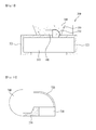
- FIG. 1 is a cross-sectional view of a conventional light emitting device.
- FIG. 2 is a top image view illustrating current spreading of the light emitting device in FIG. 1.
- FIG. 1 illustrates a cross-sectional view taken along line A-A of FIG. 2 .
- the conventional light emitting device which is designated by reference numeral "1" includes a substrate 10, and a light emitting structure 20 disposed on the substrate 10.
- the light emitting structure 20 includes a first conductivity type semiconductor layer 22, an active layer 24, and a second conductivity type semiconductor layer 26.
- the light emitting structure 20 has a mesa etching region M where portions of the second conductivity type semiconductor layer 26, active layer 24, and first conductivity type semiconductor layer 22 are removed through etching.
- a first electrode 30 is disposed on a portion of the first conductivity type semiconductor layer 22 exposed through the etching region M.
- a second electrode 40 is disposed on an unetched portion of the second conductivity type semiconductor layer 26.
- a transparent electrode layer 50 is disposed between the second conductivity type semiconductor layer 26 and the second electrode 40.
- the conventional light emitting device 1 may have a following problem.
- Embodiments provide a light emitting device exhibiting improved current spreading and a lighting apparatus including the same.
- a light emitting device includes a light emitting structure including a first conductivity type semiconductor layer, a second conductivity type semiconductor layer, and an active layer disposed between the first conductivity type semiconductor layer and the second conductivity type semiconductor layer, a first electrode disposed on the first conductivity type semiconductor layer, and a second electrode disposed on the second conductivity type semiconductor layer, wherein the light emitting structure includes a mesa etching region where the second conductivity type semiconductor layer, the active layer, and the first conductivity type semiconductor layer are partially etched, thereby exposing a portion of the first conductivity type semiconductor layer, and the first electrode is disposed on the exposed portion of the first conductivity type semiconductor layer in the mesa etching region, wherein a first electrode layer is disposed between the second conductivity type semiconductor layer and the second electrode, and a second electrode layer is disposed between portions of the first electrode layer spaced from each other at opposite sides of the mesa etching region.
- Each of the first electrode layer and the second electrode layer may be a transparent electrode layer.
- the second electrode layer may overlap, at opposite ends thereof, the first electrode layer.
- the second electrode layer may overlap a portion of the mesa etching region.
- the first electrode may be disposed beneath the second electrode layer.
- An insulating layer may be disposed between the mesa etching region and the second electrode layer.
- the insulating layer may be disposed inside a portion of the light emitting structure exposed through the mesa etching region.
- An empty space may be present between the second electrode layer and the first electrode.
- the insulating layer may fill the space between the second electrode layer and the first electrode.
- the second electrode layer may contact the first electrode layer, and may have a higher level than the first electrode layer at a location where the second electrode layer contacts the first electrode layer.
- the second electrode layer may be thicker than the first electrode layer.
- the insulating layer may enclose the first electrode.
- a light emitting device in another embodiment, includes a light emitting structure including a first conductivity type semiconductor layer, a second conductivity type semiconductor layer, and an active layer disposed between the first conductivity type semiconductor layer and the second conductivity type semiconductor layer, a first electrode disposed on the first conductivity type semiconductor layer, and a second electrode disposed on the second conductivity type semiconductor layer, wherein the light emitting structure includes a mesa etching region where the second conductivity type semiconductor layer, the active layer, and the first conductivity type semiconductor layer are partially etched, thereby exposing a portion of the first conductivity type semiconductor layer, and the first electrode is disposed on the exposed portion of the first conductivity type semiconductor layer in the mesa etching region, wherein a first electrode layer is disposed between the second conductivity type semiconductor layer and the second electrode, and a plurality of second electrode layer units is disposed between portions of the first electrode layer spaced from each other at opposite sides of the mesa etching region.
- Each of the first electrode layer and the second electrode layer may be a transparent electrode layer. Adjacent ones of the second electrode layer units may have a non-uniform spacing.
- the spacing between the second electrode layer units may be gradually reduced in a direction from a pad portion of the second electrode to an end portion of the second electrode.
- the second electrode layer units may be gradually increased in number in a direction from a pad portion of the second electrode to an end portion of the second electrode.
- the second electrode units may have non-uniform widths, respectively.
- the widths of the second electrode layer units may be gradually increased in a direction from a pad portion of the second electrode to an end portion of the second electrode.
- An insulating layer may be disposed between the mesa etching region and the second electrode layer.
- the insulating layer may be disposed inside a portion of the light emitting structure exposed through the mesa etching region.
- the insulating layer may fill a space between the second electrode layer and the first electrode.
- a lighting apparatus in another embodiment, includes a light source module including the light emitting device according to one of the above-described embodiments, a reflection plate disposed on a bottom cover, a light guide plate disposed on the reflection plate, and an optical sheet disposed on the light guide plate.
- each layer is exaggerated, omitted, or schematically illustrated for convenience of description and clarity.
- the size or area of each constituent element does not entirely reflect the actual size thereof.
- FIG. 3 is a cross-sectional view of a light emitting device according to a first embodiment.
- FIG. 4 is a plan view of the light emitting device according to the first embodiment.
- FIG. 3 illustrates a cross-sectional view taken along line B - B of FIG. 4 .
- the light emitting device may include a substrate 110, and a light emitting structure 120 disposed on the substrate 110.
- the light emitting device 100A includes a light emitting diode (LED) using a plurality of compound semiconductor layers, for example, semiconductor layers of Group III-V or Group II-VI elements.
- the LED may be a colored LED to emit blue, green, or red light, a white LED, or an ultraviolet (UV) LED.
- Light emitted from the LED may be diversified through variation of kinds and concentrations of materials constituting the semiconductor layers, although the present disclosure is not limited thereto.
- the light emitting structure 120 includes a first conductivity type semiconductor layer 122, an active layer 124, and a second conductivity type semiconductor layer 126.
- the light emitting structure 120 may be formed using, for example, metal organic chemical vapor deposition (MOCVD), chemical vapor deposition (CVD), plasma-enhanced chemical vapor deposition (PECVD), molecular beam epitaxy (MBE), hydride vapor phase epitaxy (HVPE), or the like.
- MOCVD metal organic chemical vapor deposition
- CVD chemical vapor deposition
- PECVD plasma-enhanced chemical vapor deposition
- MBE molecular beam epitaxy
- HVPE hydride vapor phase epitaxy
- the first conductivity type semiconductor layer 122 may be made of a semiconductor compound, for example, a Group III-V or Group II-VI compound semiconductor.
- the first conductivity type semiconductor layer 122 may be doped with a first conductivity type dopant.
- the first conductivity type dopant is an n-type dopant.
- the n-type dopant may include Si, Ge, Sn, Se, Te, or the like, although the present disclosure is not limited thereto.
- the first conductivity type semiconductor layer 122 is a p-type semiconductor layer
- the first conductivity type dopant is a p-type dopant.
- the p-type dopant may include Mg, Zn, Ca, Sr, Ba, or the like, although the present disclosure is not limited thereto.
- the first conductivity type semiconductor layer 122 may include a semiconductor material having a formula of Al x In y Ga 1-x-y N (0 ⁇ x ⁇ 1, 0 ⁇ y ⁇ 1, and 0 ⁇ x+y ⁇ 1).
- the first conductivity type semiconductor layer 122 may include at least one element of Ga, N, In, Al, As, and P.
- the first conductivity type semiconductor layer 122 may be made of at least one of GaN, InN, AIN, InGaN, AlGaN, InAlGaN, AlInN, AlGaAs, InGaAs, AlInGaAs, GaP, AlGaP, InGaP, AlInGaP, and InP.
- the second conductivity type semiconductor layer 126 may be made of a semiconductor compound, for example, a Group III-V or Group II-VI compound semiconductor.
- the second conductivity type semiconductor layer 126 may be doped with a second conductivity type dopant.
- the second conductivity type semiconductor layer 126 is a p-type semiconductor layer
- the second conductivity type dopant is a p-type dopant.
- the p-type dopant may include Mg, Zn, Ca, Sr, Ba, or the like, although the present disclosure is not limited thereto.
- the second conductivity type semiconductor layer 126 is an n-type semiconductor layer
- the second conductivity type dopant is an n-type dopant.
- the n-type dopant may include Si, Ge, Sn, Se, Te, or the like, although the present disclosure is not limited thereto.
- the second conductivity type semiconductor layer 126 may include a semiconductor material having a formula of Al x In y Ga 1-x-y N (0 ⁇ x ⁇ 1, 0 ⁇ y ⁇ 1, 0 ⁇ x + y ⁇ 1).
- the second conductivity type semiconductor layer 126 may include at least one element of Ga, N, In, Al, As, and P.
- the second conductivity type semiconductor layer 126 may be made of at least one of GaN, InN, AIN, InGaN, AlGaN, InAlGaN, AlInN, AlGaAs, InGaAs, AlInGaAs, GaP, AlGaP, InGaP, AlInGaP, and InP.
- first conductivity type semiconductor layer 122 is an n-type semiconductor layer
- second conductivity type semiconductor layer 126 is a p-type semiconductor layer
- a semiconductor layer having an opposite polarity to the second conductivity type may be formed over the second conductivity type semiconductor layer 126.
- the light emitting structure 120 may be implemented as one of an n-p junction structure, a p-n junction structure, an n-p-n junction structure, and a p-n-p junction structure.
- the active layer 124 is disposed between the first conductivity type semiconductor layer 122 and the second conductivity type semiconductor layer 126.
- the active layer 124 electrons and holes meet and, as such, emit light with energy determined by the intrinsic energy band of the material of the active layer 124 (light emitting layer).
- the first conductivity type semiconductor layer 122 is an n-type semiconductor layer
- the second conductivity type semiconductor layer 126 is a p-type semiconductor layer
- electrons may be injected from the first conductivity type semiconductor layer 122 into the active layer 124
- holes may be injected from the second conductivity type semiconductor layer 126 into the active layer 124.
- the active layer 124 may have at least one of a single quantum well structure, a multi quantum well structure, a quantum wire structure, and a quantum dot structure.
- the active layer 124 may have a multi quantum well structure through injection of tri-methyl gallium gas (TMGa), ammonia gas (NH 3 ), nitrogen gas (N 2 ), and tri-methyl indium gas (TMIn), although the present disclosure is not limited thereto.
- TMGa tri-methyl gallium gas
- NH 3 ammonia gas
- N 2 nitrogen gas
- TIn tri-methyl indium gas
- the active layer 124 may have well and barrier layers having at least one of layer pair structures of InGaN/GaN, InGaN/InGaN, GaN/AlGaN, InAlGaN/GaN, GaAs(InGaAs)/AlGaAs, and GaP(InGaP)/AlGaP, although the present disclosure is not limited thereto.
- the well layer may be made of a material having a lower band gap than the barrier layer.
- the light emitting structure 120 is supported by the substrate 110 disposed beneath the light emitting structure 120.
- the substrate 110 may be formed using a material suitable for growth of a semiconductor material or a material having excellent thermal conductivity.
- the substrate 110 may be made of at least one of sapphire
- Al 2 O 3 (Al 2 O 3 ), SiC, GaAs, GaN, ZnO, Si, GaP, InP, Ge, and Ga 2 O 3 .
- Wet washing or plasma treatment may be performed upon the substrate 110, to remove impurities from the surface of the substrate 110.
- a buffer layer 112 may be disposed between the light emitting structure 120 and the substrate 110.
- the buffer layer is adapted to reduce lattice mismatch and thermal expansion coefficient difference between the material of the substrate 110 and the material of the light emitting structure 120.
- the buffer layer may be made of a Group III-V or Group II-VI compound semiconductor, for example, at least one of GaN, InN, AIN, InGaN, AlGaN, InAlGaN, and AlInN.
- An undoped semiconductor layer 114 may be disposed between the substrate 110 and the first conductivity type semiconductor layer 122.
- the undoped semiconductor layer 114 is a layer formed to achieve an enhancement in crystallinity of the first conductivity type semiconductor layer 122.
- the undoped semiconductor layer 114 may be made of a material identical to or different from the material of the first semiconductor layer 122.
- the undoped semiconductor layer 114 exhibits lower electric conductivity than the first conductivity type semiconductor layer 122 because no first conductivity type dopant is doped therein.
- the undoped semiconductor layer 114 may be disposed over the buffer layer 112 while contacting the first conductivity type semiconductor layer 122.
- the undoped semiconductor layer 112 is grown at a temperature higher than the growth temperature of the buffer layer 112.
- the undoped semiconductor layer 112 exhibits higher crystallinity than the buffer layer 112.
- the light emitting structure 120 includes a mesa etching region M where portions of the second conductivity type semiconductor layer 126, active layer 124, and first conductivity type semiconductor layer 122 are removed through etching. Through the mesa etching region M, the first conductivity type semiconductor layer 122 is partially exposed.
- a first electrode 130 is disposed on the first conductivity type semiconductor layer 122.
- a second electrode 140 is disposed on the second conductivity type semiconductor layer 126.
- the first electrode 130 is disposed on the portion of the first conductivity type semiconductor layer 122 exposed through the mesa etching region M.
- the second electrode 140 is disposed on an unetched portion of the second conductivity type semiconductor layer 126.
- the first electrode layer 130 may include at least one of Mo, Cr, Ni, Au, Al, Ti, Pt, V, W, Pd, Cu, Rh, and Ir.
- the first electrode layer 120 may be formed to have a single layer structure or a multilayer structure.
- the first electrode 130 and second electrode 140 may include first and second electrode pad portions 130P and 140P having relatively large widths, respectively.
- the first and second electrode pad portions 130P and 140P may be areas to which wires (not shown) will be bonded for supply of current to the light emitting device 100A.
- An electrode layer 150 is disposed over the light emitting structure 120.
- the electrode layer 150 may be a transparent electrode layer.
- the electrode layer 150 may be disposed over the second conductivity type semiconductor layer 126 while covering at least a portion of the mesa etching region M.
- the electrode layer 150 is adapted to improve such electrical characteristics.
- the electrode layer 150 may have a layer structure or a multi pattern structure.
- the electrode layer 150 may be made of at least one of indium tin oxide (ITO), indium zinc oxide (IZO), indium zinc tin oxide (IZTO), indium aluminum zinc oxide (IAZO), indium gallium zinc oxide (IGZO), indium gallium tin oxide (IGTO), aluminum zinc oxide (AZO), antimony tin oxide (ATO), gallium zinc oxide (GZO), IZO nitride (IZON), Al-GaZnO (AGZO), In-GaZnO (IGZO), ZnO, IrO x , RuO x , NiO, RuO x /ITO, Ni/IrO x /Au, Ni/IrO x /Au/ITO, Ag, Ni, Cr, Ti, Al, Rh, Pd, Ir, Sn, In, Ru, Mg, Zn, Pt, Au, and H
- the electrode layer 150 includes a first electrode layer 151 disposed between the second conductivity type semiconductor layer 126 and the second electrode 140, and a second electrode layer 152 disposed between portions of the first electrode layer 151 spaced from each other at opposite sides of the mesa etching region M.
- the first electrode layer 151 is disposed on the unetched portion of the second conductivity type semiconductor layer 126.
- the second electrode layer 152 is disposed to correspond to the mesa etching region M.
- the second electrode layer 152 may connect the portions of the first electrode layer 151 spaced by the mesa etching region M.
- a transparent electrode layer may also be disposed in the mesa etching region M, not only to uniformly spread current injected from the second electrode 140 over the light emitting structure 120, but also to reduce a phenomenon in which current is concentrated around the second electrode 140.
- current is spread up to the mesa etching region M, an enhancement in light amount of the light emitting device 100A and an improvement in operating voltage of the light emitting device 100A may be achieved.
- the second electrode layer 152 contacts, at opposite ends thereof, the first electrode layer 151.
- opposite ends of the second electrode layer 152 may overlap the first electrode layer 151.
- the second electrode layer 152 may be thicker than the first electrode layer 151.
- the second electrode layer 152 is arranged to correspond to the mesa etching region M, which is a non-emission region, and, as such, there is no possibility of light absorption by the second electrode layer 152. Accordingly, it may be possible to maximize current spreading effects by forming the second electrode layer 152 to be thicker than the first electrode layer 151.
- the first electrode 130 is disposed beneath the second electrode layer 152.
- the second electrode layer 152 covers at least a portion of the mesa etching region M.
- the position and size of the second electrode layer 152 covering the mesa etching region M may be varied in accordance with embodiments, so long as the second electrode layer 152 connects the portions of the first electrode layer 151 spaced by the mesa etching region M.
- the second electrode layer 152 is illustrated as not being disposed over the first electrode pad portion 130P.
- the second electrode layer 152 may be arranged to completely cover the mesa etching region M or to partially cover the mesa etching region M. That is, the second electrode layer 152 may overlap a portion of the mesa etching region M.
- an insulating layer 160 may be disposed beneath the second electrode layer 152 in the mesa etching region M.
- the insulating layer 160 may also be disposed on an upper surface of the light emitting structure 120 in a region where the first electrode layer 151 is not disposed.
- the insulating layer 160 may protect side walls of the light emitting structure 120 exposed through etching while preventing electrical short circuit between the active layer 124 and the second electrode layer 152 or between the first conductivity type semiconductor layer 122 and the second electrode layer 152.
- the insulating layer 160 may be disposed at the side walls of the light emitting structure 120 exposed through mesa etching in the mesa etching region M.
- the insulating layer 160 may function to support the second electrode layer 152.
- the insulating layer 160 may be made of a non-conductive oxide or nitride.
- the insulating layer 160 may include a silicon oxide (SiO 2 ) layer, an oxide nitride layer, or an aluminum oxide layer, although the present disclosure is not limited thereto.
- the second electrode layer 152 may take the form of an air bridge.
- FIG. 5 is a plan view of a light emitting device according to a second embodiment.
- the cross-sectional view of the light emitting element of FIG. 5 taken along line B - B of FIG. 5 is identical to FIG. 3 and, as such, is not again shown and refers to FIG. 3 .
- the content of this embodiment repeating that of the previous embodiment will be no longer described and, as such, a description will be given only in conjunction with the differences of the embodiments.
- the light emitting device according to the second embodiment which is designated by reference numeral "100B" is different from the light emitting device 100A according to the first embodiment in that the second electrode layer 152 is disposed in the mesa etching region M toward an end portion E of the second electrode 140. That is, the mesa etching region M is exposed in a region adjacent to the second electrode pad portion 140P, and the second electrode 152 is disposed toward the end portion E of the second electrode 140.
- the second electrode layer 152 is disposed in the mesa etching region M toward the end portion E of the second electrode 140 and, as such, current may flow through the second electrode layer 152 before bypassing the mesa etching region M. Accordingly, smooth flow of current may be achieved.
- FIG. 6 is a plan view of a light emitting device according to a third embodiment.
- the cross-sectional view of the light emitting element of FIG. 6 taken along line B - B of FIG. 6 is identical to FIG. 3 and, as such, is not again shown and refers to FIG. 3 .
- the content of this embodiment repeating those of the previous embodiments will be no longer described and, as such, a description will be given only in conjunction with the differences of the embodiments.
- the second electrode layer 152 may include a plurality of spaced second electrode layer units 152a. Although three second electrode layer units 152a 1 , 152a 2 , and 152a 3 are illustrated in FIG. 6 , the number of second electrode layer units 152a may be varied in accordance with embodiments.
- Adjacent ones of the plural second electrode layer units 152a may be non-uniform.
- the spacing between the second electrode layer unit 152a 1 disposed at the leftmost and the second electrode layer unit 152a 2 disposed at the middle namely, a spacing D 1 differs from the spacing between the second electrode layer unit 152a 2 disposed at the middle and the second electrode layer unit 152a 3 disposed at the rightmost, namely, a spacing D 2 .
- the spacing between the adjacent two second electrode layer units 152a may be gradually reduced in a direction from the pad portion 140P of the second electrode 140 to the end portion E of the second electrode 140 (D 1 > D 2 ). That is, the number of second electrode layer units 152a may be gradually increased in the mesa etching region M in a direction toward the end portion E of the second electrode 140.
- a phenomenon in which current is concentrated occurs because current injected through the second electrode 140 flows while bypassing the mesa etching region M and, as such, smooth flow of current is not exhibited at the end portion E of the second electrode 140.
- a plurality of second electrode layer units 152a is disposed in the mesa etching region M toward the end portion E of the second electrode 140 and, as such, smooth flow of current may be achieved.
- FIG. 7 is a plan view of a light emitting device according to a fourth embodiment.
- the cross-sectional view of the light emitting element of FIG. 7 taken along line B - B of FIG. 6 is identical to FIG. 3 and, as such, is not again shown and refers to FIG. 3 .
- the content of this embodiment repeating those of the previous embodiments will be no longer described and, as such, a description will be given only in conjunction with the differences of the embodiments.
- the second electrode layer 152 may include a plurality of spaced second electrode layer units 152a. Although two second electrode layer units 152a 1 and 152a 2 are illustrated in FIG. 7 , the number of second electrode layer units 152a may be varied in accordance with embodiments.
- the plural second electrode layer units 152a may have a non-uniform width.
- the width of each second electrode layer unit 152a means a width in a direction perpendicular to a longitudinal direction of the mesa etching region M.
- the width of the second electrode layer unit 152a 1 disposed at the left side namely, a width W 1 differs from the width of the second electrode layer unit 152a 2 disposed at the right side, namely, a width W 2 .
- the widths of the plural second electrode layer units 152a may be gradually increased in a direction from the pad portion 140P of the second electrode 140 to the end portion E of the second electrode 140 (W 1 ⁇ W 2 ).
- the widths of the plural second electrode layer units 152a may be gradually increased in a direction toward the end portion E of the second electrode 140 and, as such, smooth flow of current may be achieved.
- FIG. 8 is a cross-sectional view of a light emitting device according to a fifth embodiment.
- the content of this embodiment repeating those of the previous embodiments will be no longer described and, as such, a description will be given only in conjunction with the differences of the embodiments.
- an insulating layer 160 may be disposed in the mesa etching region M.
- the insulating layer 160 may be disposed between the light emitting structure 120 and the second electrode layer 152.
- the insulating layer 160 may protect side walls of the light emitting structure 120 exposed through etching and the first electrode 130 while preventing electrical short circuit between the active layer 124 or the first conductivity type semiconductor layer 122 and the second electrode layer 152.
- the insulating layer 160 may be disposed not only at the side walls of the light emitting structure 120 exposed through mesa etching, but also between the second electrode layer 152 and the first electrode 130. That is, the insulating layer 160 may be disposed to enclose the first electrode 130 beneath the second electrode layer 152.
- the insulating layer 160 may function to more firmly support the second electrode layer 152 by filling a space between the second electrode layer 152 and the first electrode 130.
- the plan view of the light emitting device 100E according to the fifth embodiment may be similar to FIGs. 4 to 7 . Variations of the second electrode layer 152 described with reference to FIGs. 4 to 7 may also be applied to the fifth embodiment. No description will be given of such variations.
- FIG. 9 is a view illustrating a light emitting device package according to an embodiment including one of the light emitting devices according to the above-described embodiments.
- the light emitting device package according to this embodiment which is designated by reference numeral "300" includes a body 310, first and second lead frames 321 and 322 disposed at the body 310, the light emitting device 100 according to one of the above-described embodiments, which is disposed at the body 300, to be electrically connected to the first and second lead frames 321 and 322, and a mold 340 formed in a cavity, which may be formed at the body 310.
- the light emitting device 100 has a single chip structure including a plurality of light emitting cells connected in series or in parallel.
- the body 310 may be made of a silicon material, a synthetic resin material, or a metal material.
- a conductive material such as a metal material
- an insulating layer may be coated over the surface of the body 310, although not shown, in order to avoid electrical short circuit between the first and second lead frames 321 and 322 and the metal body. Accordingly, it may be possible to avoid electrical short circuit between the first lead frame 321 and the second lead frame 322.
- the first and second lead frames 321 and 322 are electrically isolated from each other, and supply current to the light emitting device 100.
- the first and second lead frames 321 and 322 may also reflect light generated from the light emitting device 100 so as to achieve an enhancement in luminous efficacy.
- the first and second lead frames 321 and 322 may function to outwardly dissipate heat generated from the light emitting device 100.
- the light emitting device 100 may be mounted on the body 310 or on the first lead frame 321 or second lead frame 322. In this embodiment, the light emitting device 100 is directly electrically connected to the first lead frame 321 while being connected to the second lead frame 322 via a wire 330. The light emitting device 100 may be electrically connected to the lead frames 321 and 322, using a flip-chip method or a die-bonding method, in place of the wire-bonding method.
- the mold 340 may encapsulate the light emitting device 100, to protect the light emitting device 100.
- the mold 340 may include phosphors 350, to change the wavelength of light emitted from the light emitting device 100.
- the phosphors 350 may include garnet-based phosphors, silicate-based phosphors, nitride-based phosphors, or oxynitride-based phosphors.
- the garnet-based phosphors may be YAG (Y 3 Al 5 O 12 :Ce 3+ ) or TAG (Tb 3 Al 5 O 12 :Ce 3+ ).
- the silicate-based phosphors may be (Sr,Ba,Mg,Ca) 2 SiO 4 :Eu 2+ .
- the nitride-based phosphors may be CaAlSiN 3 :Eu 2+ containing SiN.
- the oxynitride-based phosphors may be Si 6-x Al x O x N 8-x :Eu 2+ (0 ⁇ x ⁇ 6).
- Light of a first wavelength range emitted from the light emitting device 100 is excited by the phosphors 350 and, as such, is changed into light of a second wavelength range.
- the optical path thereof may be changed.
- a plurality of light emitting device packages each of which has the above-described structure according to the illustrated embodiment, is prepared, and is then arrayed on a substrate.
- Optical members namely, light guide plates, prism sheets, diffusion sheets, etc., may be arranged on optical paths of the light emitting device packages.
- Such light emitting device packages, substrate, and optical members may function as a light unit.
- a display apparatus, an indication apparatus or a lighting system may be implemented using the semiconductor light emitting devices or light emitting device packages described in conjunction with the above-described embodiments.
- the lighting system may include, for example, a lamp or a street lamp.
- FIG. 10 is a view illustrating a head lamp according to an embodiment, in which a light emitting device or light emitting device package according to one of the above-described embodiments is disposed.
- light emitted from a light emitting module 710 in which a light emitting device or light emitting device package according to one of the above-described embodiments is disposed, passes through a lens 740 after being reflected by a reflector 720 and a shade 730, so as to be directed forwardly of a vehicle body.
- the light emitting module 710 may include a plurality of light emitting devices mounted on a circuit board, although the present disclosure is not limited thereto.
- FIG. 11 is a view illustrating a lighting system according to an embodiment in which light emitting device packages according to the above-described embodiment are disposed.
- the lighting system includes a light source module 830-835, a reflection plate 820 disposed on a bottom cover 810, a light guide plate 840 disposed in front of the reflection plate 820, to guide light emitted from the light source module 830-835 to a front side of the lighting system 800, an optical sheet including first and second prism sheets 850 and 860 disposed in front of the light guide plate 840, a panel 870 disposed in front of the optical sheet, and a color filter 880 disposed in front of the panel 870.
- the light source module 830-835 includes a circuit board 830 and light emitting device packages 835 mounted on the circuit board 830.
- a printed circuit board PCB
- the light emitting device packages 835 may have the configuration described above in conjunction with FIG. 9 .
- the bottom cover 810 may receive the constituent elements of the lighting system 800.
- the reflection plate 820 may be provided as a separate element, as shown in FIG. 11 , or may be formed by coating material having high reflectivity over a rear surface of the light guide plate 840 or a front surface of the bottom cover 810.
- the reflection plate 820 may be made of a material having high reflectivity and capable of being formed into an ultra thin structure.
- Polyethylene terephthalate (PET) may be used for the reflection plate 820.
- the light guide plate 840 serves to scatter light emitted from the light source module 830-835 so as to uniformly distribute the light throughout all regions of the lighting system. Therefore, the light guide plate 840 may be made of a material having high refractivity and transmissivity.
- the material of the light guide plate 840 may include polymethylmethacrylate (PMMA), polycarbonate (PC), polyethylene (PE), or the like.
- PMMA polymethylmethacrylate
- PC polycarbonate
- PE polyethylene
- the light guide plate 840 may be omitted. In this case, an air guide system, which transfers light in a space over the reflective sheet 820, may be implemented.
- the first prism sheet 850 may be formed by coating a polymer exhibiting light transmittance and elasticity over one surface of a base film.
- the first prism sheet 850 may have a prism layer having a plurality of three-dimensional structures in the form of a repeated pattern.
- the pattern may be of a stripe type in which ridges and valleys are repeated.
- the second prism sheet 860 may have a similar structure to the first prism sheet 850.
- the second prism sheet 860 may be configured such that the orientation direction of ridges and valleys formed on one surface of the base film of the second prism sheet 860 is perpendicular to the orientation direction of the ridges and valleys formed on one surface of the base film of the first prism sheet 850.
- Such a configuration serves to uniformly distribute light transmitted from the light source module 830-835 and the reflective sheet 820 toward the entire surface of the panel 870.
- the optical sheet may be constituted by the first prism sheet 850 and second prism sheet 860.
- the optical sheet may include other combinations, for example, a microlens array, a combination of a diffusion sheet and a microlens array, and a combination of a prism sheet and a microlens array.
- a liquid crystal display panel may be used as the panel 870. Further, instead of the liquid crystal display panel 870, other kinds of display devices requiring light sources may be provided.
- the display panel 870 is configured such that liquid crystals are located between glass bodies, and polarizing plates are mounted on both glass bodies so as to utilize polarizing properties of light.
- the liquid crystals have properties between a liquid and a solid. That is, the liquid crystals which are organic molecules having fluidity like the liquid, are regularly oriented, and, as such, display an image using change of such molecular orientation due to an external electric field.
- the liquid crystal display panel used in the lighting system is of an active matrix type, and uses transistors as switches to adjust a voltage applied to each pixel.
- the color filter 880 is provided on the front surface of the panel 870, and transmits only a red, green or blue light component of light projected from the panel 870 per pixel, thereby displaying an image.
- current spreading up to the mesa etching region may be achieved and, as such, an enhancement in light amount of the light emitting device and an improvement in operating voltage of the light emitting device may be achieved.
Landscapes
- Engineering & Computer Science (AREA)
- Microelectronics & Electronic Packaging (AREA)
- Manufacturing & Machinery (AREA)
- Computer Hardware Design (AREA)
- Power Engineering (AREA)
- Led Devices (AREA)
Applications Claiming Priority (1)
| Application Number | Priority Date | Filing Date | Title |
|---|---|---|---|
| KR1020130070104A KR102080775B1 (ko) | 2013-06-19 | 2013-06-19 | 발광소자 |
Publications (2)
| Publication Number | Publication Date |
|---|---|
| EP2816619A1 true EP2816619A1 (de) | 2014-12-24 |
| EP2816619B1 EP2816619B1 (de) | 2019-07-31 |
Family
ID=50942612
Family Applications (1)
| Application Number | Title | Priority Date | Filing Date |
|---|---|---|---|
| EP14172944.2A Active EP2816619B1 (de) | 2013-06-19 | 2014-06-18 | Lichtemittierende Vorrichtung und entsprechende Beleuchtungsvorrichtung |
Country Status (4)
| Country | Link |
|---|---|
| US (2) | US9209363B2 (de) |
| EP (1) | EP2816619B1 (de) |
| KR (1) | KR102080775B1 (de) |
| CN (1) | CN104241487B (de) |
Cited By (1)
| Publication number | Priority date | Publication date | Assignee | Title |
|---|---|---|---|---|
| CN112786758A (zh) * | 2021-01-29 | 2021-05-11 | 錼创显示科技股份有限公司 | 微型发光二极管及显示面板 |
Families Citing this family (10)
| Publication number | Priority date | Publication date | Assignee | Title |
|---|---|---|---|---|
| KR102024295B1 (ko) * | 2013-02-05 | 2019-09-23 | 엘지이노텍 주식회사 | 발광 모듈 |
| US9666779B2 (en) * | 2013-11-25 | 2017-05-30 | Yangzhou Zhongke Semiconductor Lighting Co., Ltd. | Semiconductor light emitting diode chip with current extension layer and graphical current extension layers |
| KR102309511B1 (ko) * | 2015-01-20 | 2021-10-06 | 엘지디스플레이 주식회사 | 액정표시장치 |
| USD845920S1 (en) * | 2015-08-12 | 2019-04-16 | Epistar Corporation | Portion of light-emitting diode unit |
| TWD182762S (zh) * | 2016-02-24 | 2017-05-01 | 晶元光電股份有限公司 | 發光二極體陣列之部分 |
| TWD190563S (zh) * | 2017-06-23 | 2018-05-21 | 晶元光電股份有限公司 | 發光二極體陣列之部分 |
| KR102410809B1 (ko) * | 2017-08-25 | 2022-06-20 | 쑤저우 레킨 세미컨덕터 컴퍼니 리미티드 | 반도체 소자 |
| TWD198613S (zh) | 2018-08-08 | 2019-07-11 | 晶元光電股份有限公司 | 發光二極體之部分 |
| KR102147443B1 (ko) * | 2018-10-25 | 2020-08-28 | 엘지전자 주식회사 | 반도체 발광 소자를 이용한 디스플레이 장치 및 이의 제조방법 |
| CN110911537B (zh) * | 2019-11-29 | 2021-12-28 | 东莞市中晶半导体科技有限公司 | 共阴极led芯片及其制作方法 |
Citations (12)
| Publication number | Priority date | Publication date | Assignee | Title |
|---|---|---|---|---|
| JPH06296041A (ja) * | 1993-04-08 | 1994-10-21 | Nichia Chem Ind Ltd | 窒化ガリウム系化合物半導体発光素子 |
| US20040012030A1 (en) * | 2002-07-22 | 2004-01-22 | United Epitaxy Company, Ltd. | Structure of a light emitting diode and method of making the same |
| US20040256631A1 (en) * | 2003-06-23 | 2004-12-23 | Shin Hyoun Soo | GaN LED for flip-chip bonding and method of fabricating the same |
| EP1553640A1 (de) * | 2002-08-01 | 2005-07-13 | Nichia Corporation | Halbleiter-lichtemissionsbauelement, verfahren zu seiner herstellung und lichtemissionsvorrichtung damit |
| US20060124954A1 (en) * | 2004-10-21 | 2006-06-15 | Nichia Corporation | Semiconductor light emitting device and method for manufacturing the same |
| US20090039359A1 (en) * | 2007-08-10 | 2009-02-12 | Seoul Opto Device Co., Ltd. | Light emitting diode with improved current spreading performance |
| DE102007046743A1 (de) * | 2007-09-28 | 2009-04-02 | Osram Opto Semiconductors Gmbh | Optoelektronisches Bauelement sowie Verfahren zu dessen Herstellung |
| US20100148185A1 (en) * | 2008-12-15 | 2010-06-17 | Everlight Electronics Co., Ltd. | Flip-chip light-emitting diode device |
| EP2207211A1 (de) * | 2008-12-24 | 2010-07-14 | LG Innotek Co., Ltd. | Elektrodenstruktur für eine Leuchtdiode |
| EP2369646A1 (de) * | 2010-03-25 | 2011-09-28 | LG Innotek Co., Ltd. | Lichtemittierende Vorrichtung, Gehäuse für lichtemittierende Vorrichtung und Beleuchtungssystem |
| EP2375459A1 (de) * | 2010-04-06 | 2011-10-12 | LG Innotek Co., Ltd. | Lichtemittierende Vorrichtung, Gehäuse für lichtemittierende Vorrichtung und Beleuchtungssystem |
| JP2013048200A (ja) * | 2011-07-26 | 2013-03-07 | Mitsubishi Chemicals Corp | GaN系LED素子 |
Family Cites Families (8)
| Publication number | Priority date | Publication date | Assignee | Title |
|---|---|---|---|---|
| TW516248B (en) * | 2001-12-21 | 2003-01-01 | Epitech Technology Corp | Nitride light emitting diode with spiral-shaped metal electrode |
| KR100665116B1 (ko) * | 2005-01-27 | 2007-01-09 | 삼성전기주식회사 | Esd 보호용 led를 구비한 질화갈륨계 발광 소자 및그 제조 방법 |
| KR101428053B1 (ko) * | 2007-12-13 | 2014-08-08 | 엘지이노텍 주식회사 | 반도체 발광소자 및 그 제조방법 |
| DE102009006177A1 (de) * | 2008-11-28 | 2010-06-02 | Osram Opto Semiconductors Gmbh | Strahlungsemittierender Halbleiterchip |
| TWI470832B (zh) * | 2010-03-08 | 2015-01-21 | Lg Innotek Co Ltd | 發光裝置 |
| KR20120015651A (ko) * | 2010-08-12 | 2012-02-22 | 서울옵토디바이스주식회사 | 개선된 광 추출 효율을 갖는 발광 다이오드 |
| KR101742615B1 (ko) * | 2010-09-20 | 2017-06-01 | 엘지이노텍 주식회사 | 발광 소자 패키지 및 발광 모듈 |
| KR20130077208A (ko) * | 2011-12-29 | 2013-07-09 | 삼성전자주식회사 | 반도체 발광 소자 및 led 모듈 |
-
2013
- 2013-06-19 KR KR1020130070104A patent/KR102080775B1/ko active IP Right Grant
-
2014
- 2014-06-18 EP EP14172944.2A patent/EP2816619B1/de active Active
- 2014-06-18 US US14/308,101 patent/US9209363B2/en active Active
- 2014-06-19 CN CN201410275911.5A patent/CN104241487B/zh active Active
-
2015
- 2015-11-03 US US14/931,638 patent/US9318662B2/en active Active
Patent Citations (12)
| Publication number | Priority date | Publication date | Assignee | Title |
|---|---|---|---|---|
| JPH06296041A (ja) * | 1993-04-08 | 1994-10-21 | Nichia Chem Ind Ltd | 窒化ガリウム系化合物半導体発光素子 |
| US20040012030A1 (en) * | 2002-07-22 | 2004-01-22 | United Epitaxy Company, Ltd. | Structure of a light emitting diode and method of making the same |
| EP1553640A1 (de) * | 2002-08-01 | 2005-07-13 | Nichia Corporation | Halbleiter-lichtemissionsbauelement, verfahren zu seiner herstellung und lichtemissionsvorrichtung damit |
| US20040256631A1 (en) * | 2003-06-23 | 2004-12-23 | Shin Hyoun Soo | GaN LED for flip-chip bonding and method of fabricating the same |
| US20060124954A1 (en) * | 2004-10-21 | 2006-06-15 | Nichia Corporation | Semiconductor light emitting device and method for manufacturing the same |
| US20090039359A1 (en) * | 2007-08-10 | 2009-02-12 | Seoul Opto Device Co., Ltd. | Light emitting diode with improved current spreading performance |
| DE102007046743A1 (de) * | 2007-09-28 | 2009-04-02 | Osram Opto Semiconductors Gmbh | Optoelektronisches Bauelement sowie Verfahren zu dessen Herstellung |
| US20100148185A1 (en) * | 2008-12-15 | 2010-06-17 | Everlight Electronics Co., Ltd. | Flip-chip light-emitting diode device |
| EP2207211A1 (de) * | 2008-12-24 | 2010-07-14 | LG Innotek Co., Ltd. | Elektrodenstruktur für eine Leuchtdiode |
| EP2369646A1 (de) * | 2010-03-25 | 2011-09-28 | LG Innotek Co., Ltd. | Lichtemittierende Vorrichtung, Gehäuse für lichtemittierende Vorrichtung und Beleuchtungssystem |
| EP2375459A1 (de) * | 2010-04-06 | 2011-10-12 | LG Innotek Co., Ltd. | Lichtemittierende Vorrichtung, Gehäuse für lichtemittierende Vorrichtung und Beleuchtungssystem |
| JP2013048200A (ja) * | 2011-07-26 | 2013-03-07 | Mitsubishi Chemicals Corp | GaN系LED素子 |
Cited By (2)
| Publication number | Priority date | Publication date | Assignee | Title |
|---|---|---|---|---|
| CN112786758A (zh) * | 2021-01-29 | 2021-05-11 | 錼创显示科技股份有限公司 | 微型发光二极管及显示面板 |
| CN112786758B (zh) * | 2021-01-29 | 2023-09-26 | 錼创显示科技股份有限公司 | 微型发光二极管及显示面板 |
Also Published As
| Publication number | Publication date |
|---|---|
| KR102080775B1 (ko) | 2020-02-24 |
| CN104241487B (zh) | 2017-04-12 |
| US20140374785A1 (en) | 2014-12-25 |
| US9318662B2 (en) | 2016-04-19 |
| CN104241487A (zh) | 2014-12-24 |
| EP2816619B1 (de) | 2019-07-31 |
| KR20140147236A (ko) | 2014-12-30 |
| US20160072018A1 (en) | 2016-03-10 |
| US9209363B2 (en) | 2015-12-08 |
Similar Documents
| Publication | Publication Date | Title |
|---|---|---|
| US9318662B2 (en) | Light emitting device with improved current spreading performance and lighting apparatus including the same | |
| KR101941033B1 (ko) | 발광소자 | |
| US9356007B2 (en) | Light emitting device and lighting apparatus including the same | |
| US9112093B2 (en) | Light emitting device | |
| US20140131657A1 (en) | Light emitting device | |
| KR101908657B1 (ko) | 발광소자 | |
| KR20140008064A (ko) | 발광소자 | |
| KR102194805B1 (ko) | 발광소자 | |
| KR101991032B1 (ko) | 발광소자 | |
| KR101929933B1 (ko) | 발광 소자 및 이를 포함하는 조명 시스템 | |
| KR101922529B1 (ko) | 발광소자 | |
| KR101974153B1 (ko) | 발광 소자 및 이를 포함하는 조명 시스템 | |
| KR101902398B1 (ko) | 발광 소자 및 이를 포함하는 조명 시스템 | |
| KR20130138416A (ko) | 발광소자 | |
| KR101897003B1 (ko) | 발광소자 | |
| KR20140092092A (ko) | 발광소자 | |
| KR101883844B1 (ko) | 발광소자 | |
| KR101911865B1 (ko) | 발광소자 | |
| KR20140099618A (ko) | 발광소자 및 이를 포함한 발광소자 패키지 | |
| KR101943448B1 (ko) | 발광소자 패키지 | |
| KR102024294B1 (ko) | 발광소자 패키지 | |
| KR20130074989A (ko) | 발광소자 | |
| KR20150011118A (ko) | 발광소자 | |
| KR20140067243A (ko) | 발광소자 |
Legal Events
| Date | Code | Title | Description |
|---|---|---|---|
| PUAI | Public reference made under article 153(3) epc to a published international application that has entered the european phase |
Free format text: ORIGINAL CODE: 0009012 |
|
| 17P | Request for examination filed |
Effective date: 20140618 |
|
| AK | Designated contracting states |
Kind code of ref document: A1 Designated state(s): AL AT BE BG CH CY CZ DE DK EE ES FI FR GB GR HR HU IE IS IT LI LT LU LV MC MK MT NL NO PL PT RO RS SE SI SK SM TR |
|
| AX | Request for extension of the european patent |
Extension state: BA ME |
|
| RBV | Designated contracting states (corrected) |
Designated state(s): AL AT BE BG CH CY CZ DE DK EE ES FI FR GB GR HR HU IE IS IT LI LT LU LV MC MK MT NL NO PL PT RO RS SE SI SK SM TR |
|
| RAP1 | Party data changed (applicant data changed or rights of an application transferred) |
Owner name: LG INNOTEK CO., LTD. |
|
| STAA | Information on the status of an ep patent application or granted ep patent |
Free format text: STATUS: EXAMINATION IS IN PROGRESS |
|
| 17Q | First examination report despatched |
Effective date: 20170623 |
|
| GRAP | Despatch of communication of intention to grant a patent |
Free format text: ORIGINAL CODE: EPIDOSNIGR1 |
|
| STAA | Information on the status of an ep patent application or granted ep patent |
Free format text: STATUS: GRANT OF PATENT IS INTENDED |
|
| RIC1 | Information provided on ipc code assigned before grant |
Ipc: H01L 33/38 20100101AFI20190110BHEP Ipc: H01L 33/42 20100101ALI20190110BHEP Ipc: H01L 33/20 20100101ALN20190110BHEP |
|
| INTG | Intention to grant announced |
Effective date: 20190130 |
|
| GRAS | Grant fee paid |
Free format text: ORIGINAL CODE: EPIDOSNIGR3 |
|
| GRAA | (expected) grant |
Free format text: ORIGINAL CODE: 0009210 |
|
| STAA | Information on the status of an ep patent application or granted ep patent |
Free format text: STATUS: THE PATENT HAS BEEN GRANTED |
|
| AK | Designated contracting states |
Kind code of ref document: B1 Designated state(s): AL AT BE BG CH CY CZ DE DK EE ES FI FR GB GR HR HU IE IS IT LI LT LU LV MC MK MT NL NO PL PT RO RS SE SI SK SM TR |
|
| REG | Reference to a national code |
Ref country code: CH Ref legal event code: EP Ref country code: GB Ref legal event code: FG4D |
|
| REG | Reference to a national code |
Ref country code: AT Ref legal event code: REF Ref document number: 1161856 Country of ref document: AT Kind code of ref document: T Effective date: 20190815 |
|
| REG | Reference to a national code |
Ref country code: IE Ref legal event code: FG4D |
|
| REG | Reference to a national code |
Ref country code: DE Ref legal event code: R096 Ref document number: 602014050765 Country of ref document: DE |
|
| REG | Reference to a national code |
Ref country code: NL Ref legal event code: MP Effective date: 20190731 |
|
| REG | Reference to a national code |
Ref country code: LT Ref legal event code: MG4D |
|
| REG | Reference to a national code |
Ref country code: AT Ref legal event code: MK05 Ref document number: 1161856 Country of ref document: AT Kind code of ref document: T Effective date: 20190731 |
|
| PG25 | Lapsed in a contracting state [announced via postgrant information from national office to epo] |
Ref country code: LT Free format text: LAPSE BECAUSE OF FAILURE TO SUBMIT A TRANSLATION OF THE DESCRIPTION OR TO PAY THE FEE WITHIN THE PRESCRIBED TIME-LIMIT Effective date: 20190731 Ref country code: HR Free format text: LAPSE BECAUSE OF FAILURE TO SUBMIT A TRANSLATION OF THE DESCRIPTION OR TO PAY THE FEE WITHIN THE PRESCRIBED TIME-LIMIT Effective date: 20190731 Ref country code: AT Free format text: LAPSE BECAUSE OF FAILURE TO SUBMIT A TRANSLATION OF THE DESCRIPTION OR TO PAY THE FEE WITHIN THE PRESCRIBED TIME-LIMIT Effective date: 20190731 Ref country code: BG Free format text: LAPSE BECAUSE OF FAILURE TO SUBMIT A TRANSLATION OF THE DESCRIPTION OR TO PAY THE FEE WITHIN THE PRESCRIBED TIME-LIMIT Effective date: 20191031 Ref country code: NL Free format text: LAPSE BECAUSE OF FAILURE TO SUBMIT A TRANSLATION OF THE DESCRIPTION OR TO PAY THE FEE WITHIN THE PRESCRIBED TIME-LIMIT Effective date: 20190731 Ref country code: PT Free format text: LAPSE BECAUSE OF FAILURE TO SUBMIT A TRANSLATION OF THE DESCRIPTION OR TO PAY THE FEE WITHIN THE PRESCRIBED TIME-LIMIT Effective date: 20191202 Ref country code: NO Free format text: LAPSE BECAUSE OF FAILURE TO SUBMIT A TRANSLATION OF THE DESCRIPTION OR TO PAY THE FEE WITHIN THE PRESCRIBED TIME-LIMIT Effective date: 20191031 Ref country code: SE Free format text: LAPSE BECAUSE OF FAILURE TO SUBMIT A TRANSLATION OF THE DESCRIPTION OR TO PAY THE FEE WITHIN THE PRESCRIBED TIME-LIMIT Effective date: 20190731 Ref country code: FI Free format text: LAPSE BECAUSE OF FAILURE TO SUBMIT A TRANSLATION OF THE DESCRIPTION OR TO PAY THE FEE WITHIN THE PRESCRIBED TIME-LIMIT Effective date: 20190731 |
|
| PG25 | Lapsed in a contracting state [announced via postgrant information from national office to epo] |
Ref country code: RS Free format text: LAPSE BECAUSE OF FAILURE TO SUBMIT A TRANSLATION OF THE DESCRIPTION OR TO PAY THE FEE WITHIN THE PRESCRIBED TIME-LIMIT Effective date: 20190731 Ref country code: ES Free format text: LAPSE BECAUSE OF FAILURE TO SUBMIT A TRANSLATION OF THE DESCRIPTION OR TO PAY THE FEE WITHIN THE PRESCRIBED TIME-LIMIT Effective date: 20190731 Ref country code: AL Free format text: LAPSE BECAUSE OF FAILURE TO SUBMIT A TRANSLATION OF THE DESCRIPTION OR TO PAY THE FEE WITHIN THE PRESCRIBED TIME-LIMIT Effective date: 20190731 Ref country code: GR Free format text: LAPSE BECAUSE OF FAILURE TO SUBMIT A TRANSLATION OF THE DESCRIPTION OR TO PAY THE FEE WITHIN THE PRESCRIBED TIME-LIMIT Effective date: 20191101 Ref country code: IS Free format text: LAPSE BECAUSE OF FAILURE TO SUBMIT A TRANSLATION OF THE DESCRIPTION OR TO PAY THE FEE WITHIN THE PRESCRIBED TIME-LIMIT Effective date: 20191130 Ref country code: LV Free format text: LAPSE BECAUSE OF FAILURE TO SUBMIT A TRANSLATION OF THE DESCRIPTION OR TO PAY THE FEE WITHIN THE PRESCRIBED TIME-LIMIT Effective date: 20190731 |
|
| PG25 | Lapsed in a contracting state [announced via postgrant information from national office to epo] |
Ref country code: TR Free format text: LAPSE BECAUSE OF FAILURE TO SUBMIT A TRANSLATION OF THE DESCRIPTION OR TO PAY THE FEE WITHIN THE PRESCRIBED TIME-LIMIT Effective date: 20190731 |
|
| PG25 | Lapsed in a contracting state [announced via postgrant information from national office to epo] |
Ref country code: EE Free format text: LAPSE BECAUSE OF FAILURE TO SUBMIT A TRANSLATION OF THE DESCRIPTION OR TO PAY THE FEE WITHIN THE PRESCRIBED TIME-LIMIT Effective date: 20190731 Ref country code: DK Free format text: LAPSE BECAUSE OF FAILURE TO SUBMIT A TRANSLATION OF THE DESCRIPTION OR TO PAY THE FEE WITHIN THE PRESCRIBED TIME-LIMIT Effective date: 20190731 Ref country code: IT Free format text: LAPSE BECAUSE OF FAILURE TO SUBMIT A TRANSLATION OF THE DESCRIPTION OR TO PAY THE FEE WITHIN THE PRESCRIBED TIME-LIMIT Effective date: 20190731 Ref country code: RO Free format text: LAPSE BECAUSE OF FAILURE TO SUBMIT A TRANSLATION OF THE DESCRIPTION OR TO PAY THE FEE WITHIN THE PRESCRIBED TIME-LIMIT Effective date: 20190731 Ref country code: PL Free format text: LAPSE BECAUSE OF FAILURE TO SUBMIT A TRANSLATION OF THE DESCRIPTION OR TO PAY THE FEE WITHIN THE PRESCRIBED TIME-LIMIT Effective date: 20190731 |
|
| PG25 | Lapsed in a contracting state [announced via postgrant information from national office to epo] |
Ref country code: SM Free format text: LAPSE BECAUSE OF FAILURE TO SUBMIT A TRANSLATION OF THE DESCRIPTION OR TO PAY THE FEE WITHIN THE PRESCRIBED TIME-LIMIT Effective date: 20190731 Ref country code: IS Free format text: LAPSE BECAUSE OF FAILURE TO SUBMIT A TRANSLATION OF THE DESCRIPTION OR TO PAY THE FEE WITHIN THE PRESCRIBED TIME-LIMIT Effective date: 20200224 Ref country code: SK Free format text: LAPSE BECAUSE OF FAILURE TO SUBMIT A TRANSLATION OF THE DESCRIPTION OR TO PAY THE FEE WITHIN THE PRESCRIBED TIME-LIMIT Effective date: 20190731 Ref country code: CZ Free format text: LAPSE BECAUSE OF FAILURE TO SUBMIT A TRANSLATION OF THE DESCRIPTION OR TO PAY THE FEE WITHIN THE PRESCRIBED TIME-LIMIT Effective date: 20190731 |
|
| REG | Reference to a national code |
Ref country code: DE Ref legal event code: R097 Ref document number: 602014050765 Country of ref document: DE |
|
| PLBE | No opposition filed within time limit |
Free format text: ORIGINAL CODE: 0009261 |
|
| STAA | Information on the status of an ep patent application or granted ep patent |
Free format text: STATUS: NO OPPOSITION FILED WITHIN TIME LIMIT |
|
| PG2D | Information on lapse in contracting state deleted |
Ref country code: IS |
|
| PG25 | Lapsed in a contracting state [announced via postgrant information from national office to epo] |
Ref country code: IS Free format text: LAPSE BECAUSE OF FAILURE TO SUBMIT A TRANSLATION OF THE DESCRIPTION OR TO PAY THE FEE WITHIN THE PRESCRIBED TIME-LIMIT Effective date: 20191030 |
|
| 26N | No opposition filed |
Effective date: 20200603 |
|
| PG25 | Lapsed in a contracting state [announced via postgrant information from national office to epo] |
Ref country code: SI Free format text: LAPSE BECAUSE OF FAILURE TO SUBMIT A TRANSLATION OF THE DESCRIPTION OR TO PAY THE FEE WITHIN THE PRESCRIBED TIME-LIMIT Effective date: 20190731 |
|
| PG25 | Lapsed in a contracting state [announced via postgrant information from national office to epo] |
Ref country code: MC Free format text: LAPSE BECAUSE OF FAILURE TO SUBMIT A TRANSLATION OF THE DESCRIPTION OR TO PAY THE FEE WITHIN THE PRESCRIBED TIME-LIMIT Effective date: 20190731 |
|
| REG | Reference to a national code |
Ref country code: CH Ref legal event code: PL |
|
| GBPC | Gb: european patent ceased through non-payment of renewal fee |
Effective date: 20200618 |
|
| PG25 | Lapsed in a contracting state [announced via postgrant information from national office to epo] |
Ref country code: LU Free format text: LAPSE BECAUSE OF NON-PAYMENT OF DUE FEES Effective date: 20200618 |
|
| REG | Reference to a national code |
Ref country code: BE Ref legal event code: MM Effective date: 20200630 |
|
| PG25 | Lapsed in a contracting state [announced via postgrant information from national office to epo] |
Ref country code: LI Free format text: LAPSE BECAUSE OF NON-PAYMENT OF DUE FEES Effective date: 20200630 Ref country code: GB Free format text: LAPSE BECAUSE OF NON-PAYMENT OF DUE FEES Effective date: 20200618 Ref country code: IE Free format text: LAPSE BECAUSE OF NON-PAYMENT OF DUE FEES Effective date: 20200618 Ref country code: CH Free format text: LAPSE BECAUSE OF NON-PAYMENT OF DUE FEES Effective date: 20200630 Ref country code: FR Free format text: LAPSE BECAUSE OF NON-PAYMENT OF DUE FEES Effective date: 20200630 |
|
| PG25 | Lapsed in a contracting state [announced via postgrant information from national office to epo] |
Ref country code: BE Free format text: LAPSE BECAUSE OF NON-PAYMENT OF DUE FEES Effective date: 20200630 |
|
| REG | Reference to a national code |
Ref country code: DE Ref legal event code: R081 Ref document number: 602014050765 Country of ref document: DE Owner name: SUZHOU LEKIN SEMICONDUCTOR CO. LTD., TAICANG, CN Free format text: FORMER OWNER: LG INNOTEK CO., LTD., SEOUL, KR |
|
| PG25 | Lapsed in a contracting state [announced via postgrant information from national office to epo] |
Ref country code: MT Free format text: LAPSE BECAUSE OF FAILURE TO SUBMIT A TRANSLATION OF THE DESCRIPTION OR TO PAY THE FEE WITHIN THE PRESCRIBED TIME-LIMIT Effective date: 20190731 Ref country code: CY Free format text: LAPSE BECAUSE OF FAILURE TO SUBMIT A TRANSLATION OF THE DESCRIPTION OR TO PAY THE FEE WITHIN THE PRESCRIBED TIME-LIMIT Effective date: 20190731 |
|
| PG25 | Lapsed in a contracting state [announced via postgrant information from national office to epo] |
Ref country code: MK Free format text: LAPSE BECAUSE OF FAILURE TO SUBMIT A TRANSLATION OF THE DESCRIPTION OR TO PAY THE FEE WITHIN THE PRESCRIBED TIME-LIMIT Effective date: 20190731 |
|
| PGFP | Annual fee paid to national office [announced via postgrant information from national office to epo] |
Ref country code: DE Payment date: 20230502 Year of fee payment: 10 |