EP2816596A1 - Eingebettetes Die-Down-Paket mit Paket-auf-Paket-Vorrichtung - Google Patents
Eingebettetes Die-Down-Paket mit Paket-auf-Paket-Vorrichtung Download PDFInfo
- Publication number
- EP2816596A1 EP2816596A1 EP20140161193 EP14161193A EP2816596A1 EP 2816596 A1 EP2816596 A1 EP 2816596A1 EP 20140161193 EP20140161193 EP 20140161193 EP 14161193 A EP14161193 A EP 14161193A EP 2816596 A1 EP2816596 A1 EP 2816596A1
- Authority
- EP
- European Patent Office
- Prior art keywords
- carrier
- die
- layer
- contact points
- build
- Prior art date
- Legal status (The legal status is an assumption and is not a legal conclusion. Google has not performed a legal analysis and makes no representation as to the accuracy of the status listed.)
- Granted
Links
Images




Classifications
-
- H—ELECTRICITY
- H10—SEMICONDUCTOR DEVICES; ELECTRIC SOLID-STATE DEVICES NOT OTHERWISE PROVIDED FOR
- H10W—GENERIC PACKAGES, INTERCONNECTIONS, CONNECTORS OR OTHER CONSTRUCTIONAL DETAILS OF DEVICES COVERED BY CLASS H10
- H10W70/00—Package substrates; Interposers; Redistribution layers [RDL]
- H10W70/01—Manufacture or treatment
- H10W70/05—Manufacture or treatment of insulating or insulated package substrates, or of interposers, or of redistribution layers
-
- H—ELECTRICITY
- H10—SEMICONDUCTOR DEVICES; ELECTRIC SOLID-STATE DEVICES NOT OTHERWISE PROVIDED FOR
- H10W—GENERIC PACKAGES, INTERCONNECTIONS, CONNECTORS OR OTHER CONSTRUCTIONAL DETAILS OF DEVICES COVERED BY CLASS H10
- H10W70/00—Package substrates; Interposers; Redistribution layers [RDL]
- H10W70/01—Manufacture or treatment
- H10W70/05—Manufacture or treatment of insulating or insulated package substrates, or of interposers, or of redistribution layers
- H10W70/095—Manufacture or treatment of insulating or insulated package substrates, or of interposers, or of redistribution layers of vias therein
-
- H—ELECTRICITY
- H10—SEMICONDUCTOR DEVICES; ELECTRIC SOLID-STATE DEVICES NOT OTHERWISE PROVIDED FOR
- H10W—GENERIC PACKAGES, INTERCONNECTIONS, CONNECTORS OR OTHER CONSTRUCTIONAL DETAILS OF DEVICES COVERED BY CLASS H10
- H10W70/00—Package substrates; Interposers; Redistribution layers [RDL]
- H10W70/60—Insulating or insulated package substrates; Interposers; Redistribution layers
-
- H—ELECTRICITY
- H10—SEMICONDUCTOR DEVICES; ELECTRIC SOLID-STATE DEVICES NOT OTHERWISE PROVIDED FOR
- H10W—GENERIC PACKAGES, INTERCONNECTIONS, CONNECTORS OR OTHER CONSTRUCTIONAL DETAILS OF DEVICES COVERED BY CLASS H10
- H10W70/00—Package substrates; Interposers; Redistribution layers [RDL]
- H10W70/60—Insulating or insulated package substrates; Interposers; Redistribution layers
- H10W70/611—Insulating or insulated package substrates; Interposers; Redistribution layers for connecting multiple chips together
-
- H—ELECTRICITY
- H10—SEMICONDUCTOR DEVICES; ELECTRIC SOLID-STATE DEVICES NOT OTHERWISE PROVIDED FOR
- H10W—GENERIC PACKAGES, INTERCONNECTIONS, CONNECTORS OR OTHER CONSTRUCTIONAL DETAILS OF DEVICES COVERED BY CLASS H10
- H10W70/00—Package substrates; Interposers; Redistribution layers [RDL]
- H10W70/60—Insulating or insulated package substrates; Interposers; Redistribution layers
- H10W70/611—Insulating or insulated package substrates; Interposers; Redistribution layers for connecting multiple chips together
- H10W70/614—Insulating or insulated package substrates; Interposers; Redistribution layers for connecting multiple chips together the multiple chips being integrally enclosed
-
- H—ELECTRICITY
- H10—SEMICONDUCTOR DEVICES; ELECTRIC SOLID-STATE DEVICES NOT OTHERWISE PROVIDED FOR
- H10W—GENERIC PACKAGES, INTERCONNECTIONS, CONNECTORS OR OTHER CONSTRUCTIONAL DETAILS OF DEVICES COVERED BY CLASS H10
- H10W70/00—Package substrates; Interposers; Redistribution layers [RDL]
- H10W70/60—Insulating or insulated package substrates; Interposers; Redistribution layers
- H10W70/62—Insulating or insulated package substrates; Interposers; Redistribution layers characterised by their interconnections
- H10W70/63—Vias, e.g. via plugs
- H10W70/635—Through-vias
-
- H—ELECTRICITY
- H10—SEMICONDUCTOR DEVICES; ELECTRIC SOLID-STATE DEVICES NOT OTHERWISE PROVIDED FOR
- H10W—GENERIC PACKAGES, INTERCONNECTIONS, CONNECTORS OR OTHER CONSTRUCTIONAL DETAILS OF DEVICES COVERED BY CLASS H10
- H10W70/00—Package substrates; Interposers; Redistribution layers [RDL]
- H10W70/60—Insulating or insulated package substrates; Interposers; Redistribution layers
- H10W70/67—Insulating or insulated package substrates; Interposers; Redistribution layers characterised by their insulating layers or insulating parts
- H10W70/68—Shapes or dispositions thereof
- H10W70/685—Shapes or dispositions thereof comprising multiple insulating layers
-
- H—ELECTRICITY
- H10—SEMICONDUCTOR DEVICES; ELECTRIC SOLID-STATE DEVICES NOT OTHERWISE PROVIDED FOR
- H10W—GENERIC PACKAGES, INTERCONNECTIONS, CONNECTORS OR OTHER CONSTRUCTIONAL DETAILS OF DEVICES COVERED BY CLASS H10
- H10W72/00—Interconnections or connectors in packages
-
- H—ELECTRICITY
- H10—SEMICONDUCTOR DEVICES; ELECTRIC SOLID-STATE DEVICES NOT OTHERWISE PROVIDED FOR
- H10W—GENERIC PACKAGES, INTERCONNECTIONS, CONNECTORS OR OTHER CONSTRUCTIONAL DETAILS OF DEVICES COVERED BY CLASS H10
- H10W90/00—Package configurations
-
- H—ELECTRICITY
- H05—ELECTRIC TECHNIQUES NOT OTHERWISE PROVIDED FOR
- H05K—PRINTED CIRCUITS; CASINGS OR CONSTRUCTIONAL DETAILS OF ELECTRIC APPARATUS; MANUFACTURE OF ASSEMBLAGES OF ELECTRICAL COMPONENTS
- H05K1/00—Printed circuits
- H05K1/18—Printed circuits structurally associated with non-printed electric components
- H05K1/182—Printed circuits structurally associated with non-printed electric components associated with components mounted in printed circuit boards [PCB], e.g. insert-mounted components [IMC]
- H05K1/185—Printed circuits structurally associated with non-printed electric components associated with components mounted in printed circuit boards [PCB], e.g. insert-mounted components [IMC] associated with components encapsulated in the insulating substrate of the PCBs; associated with components incorporated in internal layers of multilayer circuit boards
-
- H—ELECTRICITY
- H05—ELECTRIC TECHNIQUES NOT OTHERWISE PROVIDED FOR
- H05K—PRINTED CIRCUITS; CASINGS OR CONSTRUCTIONAL DETAILS OF ELECTRIC APPARATUS; MANUFACTURE OF ASSEMBLAGES OF ELECTRICAL COMPONENTS
- H05K2201/00—Indexing scheme relating to printed circuits covered by H05K1/00
- H05K2201/10—Details of components or other objects attached to or integrated in a printed circuit board
- H05K2201/10613—Details of electrical connections of non-printed components, e.g. special leads
- H05K2201/10621—Components characterised by their electrical contacts
- H05K2201/10674—Flip chip
-
- H—ELECTRICITY
- H05—ELECTRIC TECHNIQUES NOT OTHERWISE PROVIDED FOR
- H05K—PRINTED CIRCUITS; CASINGS OR CONSTRUCTIONAL DETAILS OF ELECTRIC APPARATUS; MANUFACTURE OF ASSEMBLAGES OF ELECTRICAL COMPONENTS
- H05K3/00—Apparatus or processes for manufacturing printed circuits
- H05K3/46—Manufacturing multilayer circuits
- H05K3/4644—Manufacturing multilayer circuits by building the multilayer layer by layer, i.e. build-up multilayer circuits
- H05K3/4682—Manufacture of core-less build-up multilayer circuits on a temporary carrier or on a metal foil
-
- H—ELECTRICITY
- H10—SEMICONDUCTOR DEVICES; ELECTRIC SOLID-STATE DEVICES NOT OTHERWISE PROVIDED FOR
- H10W—GENERIC PACKAGES, INTERCONNECTIONS, CONNECTORS OR OTHER CONSTRUCTIONAL DETAILS OF DEVICES COVERED BY CLASS H10
- H10W70/00—Package substrates; Interposers; Redistribution layers [RDL]
- H10W70/01—Manufacture or treatment
- H10W70/05—Manufacture or treatment of insulating or insulated package substrates, or of interposers, or of redistribution layers
- H10W70/08—Manufacture or treatment of insulating or insulated package substrates, or of interposers, or of redistribution layers by depositing layers on the chip or wafer, e.g. "chip-first" RDLs
- H10W70/09—Manufacture or treatment of insulating or insulated package substrates, or of interposers, or of redistribution layers by depositing layers on the chip or wafer, e.g. "chip-first" RDLs extending onto an encapsulation that laterally surrounds the chip or wafer, e.g. fan-out wafer level package [FOWLP] RDLs
-
- H—ELECTRICITY
- H10—SEMICONDUCTOR DEVICES; ELECTRIC SOLID-STATE DEVICES NOT OTHERWISE PROVIDED FOR
- H10W—GENERIC PACKAGES, INTERCONNECTIONS, CONNECTORS OR OTHER CONSTRUCTIONAL DETAILS OF DEVICES COVERED BY CLASS H10
- H10W70/00—Package substrates; Interposers; Redistribution layers [RDL]
- H10W70/01—Manufacture or treatment
- H10W70/05—Manufacture or treatment of insulating or insulated package substrates, or of interposers, or of redistribution layers
- H10W70/093—Connecting or disconnecting other interconnections thereto or therefrom, e.g. connecting bond wires or bumps
-
- H—ELECTRICITY
- H10—SEMICONDUCTOR DEVICES; ELECTRIC SOLID-STATE DEVICES NOT OTHERWISE PROVIDED FOR
- H10W—GENERIC PACKAGES, INTERCONNECTIONS, CONNECTORS OR OTHER CONSTRUCTIONAL DETAILS OF DEVICES COVERED BY CLASS H10
- H10W72/00—Interconnections or connectors in packages
- H10W72/20—Bump connectors, e.g. solder bumps or copper pillars; Dummy bumps; Thermal bumps
- H10W72/241—Dispositions, e.g. layouts
-
- H—ELECTRICITY
- H10—SEMICONDUCTOR DEVICES; ELECTRIC SOLID-STATE DEVICES NOT OTHERWISE PROVIDED FOR
- H10W—GENERIC PACKAGES, INTERCONNECTIONS, CONNECTORS OR OTHER CONSTRUCTIONAL DETAILS OF DEVICES COVERED BY CLASS H10
- H10W72/00—Interconnections or connectors in packages
- H10W72/851—Dispositions of multiple connectors or interconnections
- H10W72/874—On different surfaces
- H10W72/884—Die-attach connectors and bond wires
-
- H—ELECTRICITY
- H10—SEMICONDUCTOR DEVICES; ELECTRIC SOLID-STATE DEVICES NOT OTHERWISE PROVIDED FOR
- H10W—GENERIC PACKAGES, INTERCONNECTIONS, CONNECTORS OR OTHER CONSTRUCTIONAL DETAILS OF DEVICES COVERED BY CLASS H10
- H10W72/00—Interconnections or connectors in packages
- H10W72/90—Bond pads, in general
- H10W72/941—Dispositions of bond pads
- H10W72/9413—Dispositions of bond pads on encapsulations
-
- H—ELECTRICITY
- H10—SEMICONDUCTOR DEVICES; ELECTRIC SOLID-STATE DEVICES NOT OTHERWISE PROVIDED FOR
- H10W—GENERIC PACKAGES, INTERCONNECTIONS, CONNECTORS OR OTHER CONSTRUCTIONAL DETAILS OF DEVICES COVERED BY CLASS H10
- H10W74/00—Encapsulations, e.g. protective coatings
-
- H—ELECTRICITY
- H10—SEMICONDUCTOR DEVICES; ELECTRIC SOLID-STATE DEVICES NOT OTHERWISE PROVIDED FOR
- H10W—GENERIC PACKAGES, INTERCONNECTIONS, CONNECTORS OR OTHER CONSTRUCTIONAL DETAILS OF DEVICES COVERED BY CLASS H10
- H10W74/00—Encapsulations, e.g. protective coatings
- H10W74/10—Encapsulations, e.g. protective coatings characterised by their shape or disposition
-
- H—ELECTRICITY
- H10—SEMICONDUCTOR DEVICES; ELECTRIC SOLID-STATE DEVICES NOT OTHERWISE PROVIDED FOR
- H10W—GENERIC PACKAGES, INTERCONNECTIONS, CONNECTORS OR OTHER CONSTRUCTIONAL DETAILS OF DEVICES COVERED BY CLASS H10
- H10W74/00—Encapsulations, e.g. protective coatings
- H10W74/10—Encapsulations, e.g. protective coatings characterised by their shape or disposition
- H10W74/131—Encapsulations, e.g. protective coatings characterised by their shape or disposition the semiconductor body being only partially enclosed
- H10W74/142—Encapsulations, e.g. protective coatings characterised by their shape or disposition the semiconductor body being only partially enclosed the encapsulations exposing the passive side of the semiconductor body
-
- H—ELECTRICITY
- H10—SEMICONDUCTOR DEVICES; ELECTRIC SOLID-STATE DEVICES NOT OTHERWISE PROVIDED FOR
- H10W—GENERIC PACKAGES, INTERCONNECTIONS, CONNECTORS OR OTHER CONSTRUCTIONAL DETAILS OF DEVICES COVERED BY CLASS H10
- H10W90/00—Package configurations
- H10W90/20—Configurations of stacked chips
- H10W90/28—Configurations of stacked chips the stacked chips having different sizes, e.g. chip stacks having a pyramidal shape
-
- H—ELECTRICITY
- H10—SEMICONDUCTOR DEVICES; ELECTRIC SOLID-STATE DEVICES NOT OTHERWISE PROVIDED FOR
- H10W—GENERIC PACKAGES, INTERCONNECTIONS, CONNECTORS OR OTHER CONSTRUCTIONAL DETAILS OF DEVICES COVERED BY CLASS H10
- H10W90/00—Package configurations
- H10W90/20—Configurations of stacked chips
- H10W90/291—Configurations of stacked chips characterised by containers, encapsulations, or other housings for the stacked chips
-
- H—ELECTRICITY
- H10—SEMICONDUCTOR DEVICES; ELECTRIC SOLID-STATE DEVICES NOT OTHERWISE PROVIDED FOR
- H10W—GENERIC PACKAGES, INTERCONNECTIONS, CONNECTORS OR OTHER CONSTRUCTIONAL DETAILS OF DEVICES COVERED BY CLASS H10
- H10W90/00—Package configurations
- H10W90/701—Package configurations characterised by the relative positions of pads or connectors relative to package parts
- H10W90/721—Package configurations characterised by the relative positions of pads or connectors relative to package parts of bump connectors
- H10W90/722—Package configurations characterised by the relative positions of pads or connectors relative to package parts of bump connectors between stacked chips
-
- H—ELECTRICITY
- H10—SEMICONDUCTOR DEVICES; ELECTRIC SOLID-STATE DEVICES NOT OTHERWISE PROVIDED FOR
- H10W—GENERIC PACKAGES, INTERCONNECTIONS, CONNECTORS OR OTHER CONSTRUCTIONAL DETAILS OF DEVICES COVERED BY CLASS H10
- H10W90/00—Package configurations
- H10W90/701—Package configurations characterised by the relative positions of pads or connectors relative to package parts
- H10W90/731—Package configurations characterised by the relative positions of pads or connectors relative to package parts of die-attach connectors
- H10W90/732—Package configurations characterised by the relative positions of pads or connectors relative to package parts of die-attach connectors between stacked chips
-
- H—ELECTRICITY
- H10—SEMICONDUCTOR DEVICES; ELECTRIC SOLID-STATE DEVICES NOT OTHERWISE PROVIDED FOR
- H10W—GENERIC PACKAGES, INTERCONNECTIONS, CONNECTORS OR OTHER CONSTRUCTIONAL DETAILS OF DEVICES COVERED BY CLASS H10
- H10W90/00—Package configurations
- H10W90/701—Package configurations characterised by the relative positions of pads or connectors relative to package parts
- H10W90/731—Package configurations characterised by the relative positions of pads or connectors relative to package parts of die-attach connectors
- H10W90/734—Package configurations characterised by the relative positions of pads or connectors relative to package parts of die-attach connectors between a chip and a stacked insulating package substrate, interposer or RDL
-
- H—ELECTRICITY
- H10—SEMICONDUCTOR DEVICES; ELECTRIC SOLID-STATE DEVICES NOT OTHERWISE PROVIDED FOR
- H10W—GENERIC PACKAGES, INTERCONNECTIONS, CONNECTORS OR OTHER CONSTRUCTIONAL DETAILS OF DEVICES COVERED BY CLASS H10
- H10W90/00—Package configurations
- H10W90/701—Package configurations characterised by the relative positions of pads or connectors relative to package parts
- H10W90/751—Package configurations characterised by the relative positions of pads or connectors relative to package parts of bond wires
- H10W90/754—Package configurations characterised by the relative positions of pads or connectors relative to package parts of bond wires between a chip and a stacked insulating package substrate, interposer or RDL
Definitions
- BBUL packaging technology including methods to mechanically and electrically attach a silicon die (e.g., a microprocessor) to a substrate or other carrier continues to be refined and improved.
- Bumpless Build-Up Layer (BBUL) packaging technology is one approach to a packaging architecture.
- BBUL packaging technology eliminates the need for assembly, eliminates prior solder ball interconnections (e.g., flip-chip interconnections), reduces stress on low-k interlayer dielectric of dies due to die-to-substrate coefficient of thermal expansion (CTE mismatch), and reduces package inductance through elimination of core and flip-chip interconnect for improved input/output (I/O) and power delivery performance.
- I/O input/output
- POP package on package
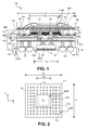
- FIG. 1 shows a cross-sectional view of a package on package (POP) device integration apparatus or assembly according to one embodiment.
- assembly 100 includes microelectronic package 110 that utilizes bumpless build-up layer (BBUL) packaging technology.
- Microelectronic package 110 includes carrier 120.
- Carrier 120 includes die 130, such as a microprocessor die or a system on chip (SOC) die, embedded in the carrier device side up (as viewed).
- die 130 is a silicon die or the like having a thickness of approximately 150 micrometers ( ⁇ m).
- die 130 can be a silicon die or the like that has a thickness less than 150 ⁇ m such as 50 ⁇ m to 150 ⁇ m.
- Die 130 is positioned, in this view, at a base of carrier 120 (a "die down" configuration).
- Figure 1 shows carrier 120 including multiple build-up layers including dielectric layers 140A, 140B, 140C, 140D and 140E of, for example, Ajinomoto build-up film (ABF) (e.g., dielectric layers 140A, 140B and 140C) or glass film (e.g., dielectric layers 140D and 140E) and electrically conductive layers or lines 150A, 150B, 150C and 150D (four shown) of, for example, copper or a copper alloy (connected with conductive vias or the like) that provide connectivity to die 130 (power, ground, input/output, etc.) through contacts 155 such as, for example, contacts suitable for a surface mount packaging implementation (e.g., a ball grid array).
- ABSF Ajinomoto build-up film
- dielectric layers 140A, 140B and 140C glass film
- electrically conductive layers or lines 150A, 150B, 150C and 150D four shown
- contacts 155 such as, for example, contacts suitable for a surface mount packaging implementation (e.g.,
- Dielectric layers 140A-D are respectively disposed between conductive layers 150A-D to insulate the conductive layers (i.e., the conductive material layers or lines and the dielectric material layers alternate in a stack from bottom to top as viewed).
- Die 130 and carrier 120 are in direct physical contact with each other (e.g., there are no solder bumps connecting die 130 to carrier 120).
- Die 130 is directly electronically connected through conductive pillars 160 to conductive vias 165 of carrier 120.
- adhesive layer 135 of, for example, a die backside film (DBF) polymer, an epoxy based dielectric adhesive with or without fillers.
- DPF die backside film
- dielectric layer 140A surrounds the lateral sidewalls of die 130. In this manner, dielectric layer 140A embeds at least a portion of a thickness dimension of die 130. In the embodiment shown in Figure 1 , dielectric layer 140A embeds a portion of the lateral sidewall of die 130. In this embodiment, dielectric layer 140A also embeds the entire portion of a thickness dimension of adhesive layer 135.
- microelectronic package 110 is configured to be connected to a printed circuit board at a base or die side of the package.
- carrier 120 includes contact points or pads 155 at its base for connection to a printed circuit board.
- Contact points or pads 155 are connected to conductive layer or line 150A (first level) through conductive vias 157 through dielectric layer 140A.
- Figure 1 shows a surface-mount packaging, such as a ball grid array (BGA) to mount microelectronic package to, for example, a printed circuit board or other board.
- BGA ball grid array
- solder material 148 e.g., solder balls
- contact points or pad 155 of carrier 120 in connection of microelectronic package 110 to a substrate, such as a printed circuit board the contact points or pads are recessed or set-off in a different plane of dielectric layer 140A than a portion of the package including die 130.
- contact points or pads 155 are disposed at a plane or gradation between a device side of the die and the embedded thickness dimension of the die.
- Figure 1 shows dielectric layer 140A defining gradation 1400A at a base of microelectronic package 110 defined by the dielectric material or the dielectric layer embedding a thickness dimension of adhesive layer 135.
- dielectric layer 140A that embeds adhesive layer 135 and a portion of the lateral sidewalls of die 130 does not extend a width dimension, W 1 , of carrier 120. Instead, that portion of dielectric layer 140A extends a width dimension, W 2 , that is at least sufficient to surround the lateral sidewalls of die 130 but not sufficient to cover contact points or pads 155.
- Dielectric layer 140A also defines gradation 1400B, a distance from gradation 1400A. Contact points or pads 155 are exposed at gradation 1400B.
- the difference between a plane of gradation 1400A and gradation 1400B creates cavity 145 at base of assembly 100 between the carrier portion of the package and a substrate (e.g., a printed circuit board).
- cavity 145 surrounds die 130. Disposed within cavity 145 are solder material
- a z-dimension length i.e., a z-height
- the transition from gradation 1400A and 1400B is illustrated as a vertical line. It is appreciated that the transition may be other than vertical (e.g., a slope between 45° and 90° from 1400A to 1400B) and may be the result of tooling.
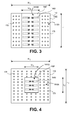
- Figure 2 shows a cross-sectional view the package of Figure 1 through line 2-2'.
- Figure 2 shows gradation 1400A and gradation 1400B in dielectric layer 140A.
- cavity 145 created by the difference in gradations of dielectric layer 140A and including solder material 148 (e.g., solder balls) extends about each lateral side of die 130.
- cavity 145 may be two separate cavities, one on each side of opposing lateral sidewalls of die 130 such that gradation 1400A on dielectric layer 140A extends an entire width dimension (x-direction) or length dimension (y-direction) of microelectronic package 110.
- Figure 2 also shows a single die, die 130, in microelectronic package 110. It is appreciated that, in another embodiment, another die or dies may be included in microelectronic package 110, such as arranged along a width or length dimension of microelectronic package 110.
- Figure 1 shows alternating layers of conductive material and dielectric material.
- assembly 100 includes four layers or lines of conductive material (e.g., conductive layers 150A, 150B, 150C and 150D).
- Conductive layer or line 150D is the ultimate layer in the sense that it is the layer aligned furthest from die 130.
- Conductive layer 150C is the penultimate layer.
- conductive layer or line 150C is patterned to include contact points 158 for connection to a secondary device (e.g., a package, a die).
- a plane of dielectric layer 140D defines gradation 1410A at contact points 158.
- dielectric layer 140E Between penultimate conductive layer 150C and ultimate conductive layer 150D is dielectric layer 140E.
- dielectric layer 140F On ultimate conductive layer 150D is dielectric layer 140F.
- a plane of dielectric layer 140F defines gradation 1410B a distance from the plane of gradation 1410A.
- contact points 158 are disposed at gradation 1410A between the ultimate conductive layer (conductive layer 150D) and the die and more specifically, in one embodiment, at the penultimate conductive layer (conductive layer 150C) or at dielectric layer 140D.
- the transition from gradation 1410A to 1410B is shown as a vertical line, but in other embodiments may be other than vertical (e.g., a slope between 45° and 90°).
- a width dimension (x-direction) of dielectric layers 140A-C and conductive layers 150A-D of carrier 120 is represented by width, W 1 .
- W 1 is greater than a width dimension of dielectric layers 140E-F and patterned conductive layer 150D, a width dimension of dielectric layers 140E and 140F represent as width, W 3 .
- the difference in width dimensions (W 1 -W 3 ) creates cavity 170 between microelectronic package 110 and a secondary device, such as package 180 shown connected to microelectronic package 110 in Figure 1 .
- package 180 is connected to microelectronic package 110 through solder material connections 178 (e.g., solder balls) at contact points 158. Solder material connections 178 to contact points 158 and to package 180 occur in cavity 170. Because solder material connections 178 are disposed within cavity 170, the height or z-dimension of assembly 100 is reduced over a z-dimension without cavity 170.
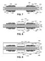
- Figure 3 shows a cross-sectional view of microelectronic package 110 through line 3-3'.
- the cross-sectional view illustrates gradation 1410A and gradation 1410B.
- microelectronic package 110 includes gradation 1410B extending a length dimension, L 1 , across microelectronic package 110 and a width dimension, W 3 , that is less than an entire width dimension, W 1 , of the package.
- Gradation 1410A and associated cavity 170 is disposed on opposing lateral sides of the cross-sectional area associated with gradation 1410B (i.e., the lateral sides of dielectric layer 140E and dielectric layer 140F).
- Figure 3 also shows solder material connections 178 disposed on contact points or pads 158 of package 110 in areas of gradation 1410A. It is appreciated that the number of contact points or pads 158 may vary according to the requirements of the device or devices to be attached to package 110.
- Figure 4 shows an alternative embodiment of package 110 through line 3-3'.
- gradation 1410B extends a length dimension, L 2 , that is less than an entire length dimension, L 1 of the package.
- an area covered by gradation 1410A is larger because such area can be disposed adjacent each of the four lateral sides of gradation 1410B.
- the larger area of gradation 1410A allows for the placement of additional contact points or pads and the associated increased solder material connections 178 as may be necessary depending on, for example, the requirements of a secondary device or devices to be connected to package 110.
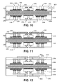
- Figures 5-22 describe one embodiment for forming a microelectronic package, such as microelectronic package 110 ( Figure 1 ).
- Figure 5 shows an exploded cross-sectional side view of a portion of sacrificial substrate 210 of, for example, a prepeg material including opposing layers of copper foils 215A and 215B that are separated from sacrificial substrate 210 by shorter copper foil layers 220A and 220B, respectively. Copper foils 215A and 215B tend to stick to the shorter foils based on vacuum.
- Figure 6 shows the assembled structure of Figure 5 .
- One technique of forming build-up packages is to form two separate packages or a sacrificial substrate, one on a top surface of sacrificial substrate 210 and one on a bottom surface (as viewed). At some point during the formation process, the two packages are separated from sacrificial substrate 210. The following formation process follows this technique.
- Figure 7 shows the structure of Figure 6 following the introduction of dielectric material layer 225A and dielectric material layer 225B on foil layer 215A and foil layer 215B, respectively.
- dielectric material layer 225A/225B is an ABF material introduced as a film over the respective surfaces of the substrate.
- a suitable thickness for dielectric material layer 225A/225B is on the order of 20 microns.
- spacer layer 230A and spacer layer 230B are spacer layer 230A and spacer layer 230B.
- spacer layer 230A/230B is a copper material (e.g., copper or a copper alloy) having a thickness selected for a thickness or depth of a cavity on a substrate connection side of a package (e.g., cavity 145 in Figure 1 ).
- a representative thickness dimension is on the order of 50 microns to 65 microns.
- spacer layer 230A/230B is introduced across the surface of the structure (e.g., as a film (laminated film)) and then patterned to a length and width dimension of the desired cavity or cavities.
- One representative patterning technique is to introduce a light sensitive material such as a dry film resist (DFR) material; expose the light sensitive material to a light source through a mask to render a portion of the light sensitive material soluble in a developer; remove the soluble portion of the light sensitive material with a developer to leave a patterned light sensitive material layer; etch spacer layer 230A/230B through the patterned light sensitive material layer; and remove the light sensitive material layer.
- a light sensitive material such as a dry film resist (DFR) material
- DFR dry film resist
- contact pads 235A and contact pads 235B are, for example, a gold material (e.g., gold, gold alloy) deposited using an electroless seed layer followed by a dry film resist (DFR) patterning and plating.
- Contact pads 235A/235B are configured for connection of the package to a substrate such as a printed circuit board (e.g., contact pads 155 in Figure 1 ). The number and position of the pads will therefore be dictated, at least in part, by the requirements of connection of the package to a substrate.
- secondary pad material 236A and secondary pad material 236B such as copper (e.g., copper, copper alloy) also deposited using a plating technique.
- copper e.g., copper, copper alloy
- alternative surface finishing layers e.g., nickel and/or palladium may be added such as in between contact pads 235A/235B and secondary pad material 236A/236B to, for example, improve solder joint reliability.
- Figure 8 shows the structure of Figure 7 following the mounting of die 240A and die 240B on opposite sides of the structure.
- die 240A is attached to adhesive 250A and die 240B is attached to adhesive 250B.
- a suitable adhesive material for 250A and adhesive 250B is DBF.
- Die 240A and die 240B are positioned device side up (device side facing away from each copper foil).
- Figure 8 shows that conductive pillars 245A and 245B are connected to the contact points of die 240A and die 240B, respectively. Pillars 245A and pillars 245B may be fabricated at the die fabrication stage.
- Figure 9 shows the structure of Figure 8 following the introduction of a dielectric layer on each side of the structure.
- Figure 9 shows dielectric layer 260A and dielectric layer 260B.
- dielectric layer 260A and dielectric layer 260B are each an ABF dielectric material possibly including a filler that have been described for use in forming a BBUL package.
- One method of introduction of an ABF material is as a film that is laid on the respective dice, the contacts and copper foils.
- Figure 10 shows the structure of Figure 9 following the opening of vias 262A and 262B in dielectric layer 260A and dielectric layer 260B to contacts 236A, contacts 236B, pillars 245A and pillars 245B.
- openings or vias may be achieved by a laser process.
- Figure 11 shows the structure of Figure 10 following the patterning of a conductive line or layer 275A and conductive line or layer 275B on dielectric layer 260A and dielectric layer 260B, respectively, and conductive vias 265A and 265B formed through the respective dielectric layers to contacts 236A and contacts 236B, respectively. Conductive vias are also formed to pillars 245A and pillars 245B to contact points on a device side of die 240A and die 240B.
- a suitable material for patterned conductive line or layer 275A/275B and for conductive vias 265A/265B is copper deposited, for example, by an electroplating process.
- Figure 12 shows the structure of Figure 11 following the patterning of an additional level of conductive line or layer of a carrier.
- Figure 12 shows conductive line or layer 280A and conductive line or layer 280B separated from conductive line or layer 275A and 275B, respectively by dielectric layer 278A and 278B, respectively (e.g., an ABF film).
- a typical BBUL package may have four to six levels of conductive lines or traces similar to conductive lines or layers 275A, 275B, 280A and 280B separated from adjacent lines by dielectric material (e.g., ABF film). Connections between the layers are made, in one embodiment, by conductive vias (e.g., copper filled vias) formed by laser drilling the vias and depositing a conductive material in the vias by way of an electroplating process.
- conductive vias e.g., copper filled vias
- Figure 13 shows the structure of Figure 12 following the introduction and patterning of conductive lines or layers 285A and 285B (third level).
- at least a portion of conductive lines or layers are patterned into lands or pads for packaging implementation (e.g., to connect to an external component such as a package or die) while another portion of lines or layers 290A and 290B are patterned to route signals.
- Figure 13 also shows the structure after the introduction of dielectric layer 282A and dielectric layer 282B on respective sides of the structure.
- dielectric layer 282A/282B is a glass cloth (ABF glass cloth) introduced or laminated as a film or sheet across the surface of the structure. Glass cloth has a property that renders the dielectric layer stiffer than a conventional ABF layer.
- dielectric layer 282A/282B is a conventional ABF layer.
- dielectric layer 282A and dielectric layer 282B are laminated on conductive line or layer 285A and conductive line or layer 285B, respectively.
- Figure 14 shows the structure of Figure 13 following the introduction of spacer layer 290A and spacer layer 290B on conductive line 285A and conductive line 285B and dielectric layer 282A and dielectric layer 282B.
- spacer layer 290A and spacer layer 290B are a copper material (e.g., copper or copper alloy) introduced by lamination and/or hot press process.
- the copper material is introduced to a thickness selected for a cavity to be formed between a microelectronic package that is being formed and a secondary device, such as a secondary package or substrate (e.g., cavity 170 between package 110 and secondary device 180 in Figure 1 ).
- a representative thickness is on the order of 70 microns.
- Figure 15 shows the structure of Figure 14 following the introduction of a light sensitive material such as a dry film resist (DFR) on the structure.
- Figure 15 shows DFR layer 292A on spacer layer 290A and DFR layer 292B on spacer layer 290B.
- each DFR layer is exposed to ultraviolet light through a mask (mask 294A and mask 294B, respectively) to render a portion the DFR layer soluble to a developer.
- portion 293A and portion 293B are exposed to the ultraviolet light.
- portion 293A of DFR layer 292A and portion 293B of DFR layer 292B is selected, in one embodiment, based on an area of the microelectronic package in which a cavity is not to be formed (e.g., an area represented by width W 3 in Figure 1 ).
- portion 293A and portion 293B are removed with a developer to produce a pattern that can be transferred to spacer layer 290A and spacer layer 290B.
- Figure 16 shows the structure of Figure 15 following the removal of material from an area of spacer layer 290A (area 291A) and spacer layer 290B (area 291B) using the respective patterned DFR layer.
- the removal may be done by an etch process.
- Figure 16 also shows the structure after the removal of the DFR layer.
- Figure 17 shows the structure of Figure 16 following the introduction and patterning of a dielectric material in area 291A and area 291B, respectively.
- the dielectric material is glass cloth introduced as a film.
- Figure 17 shows dielectric layer 296A and dielectric layer 296B of, for example, glass cloth patterned with vias openings to patterned conductive layer or line 285A and conductive layer or line 285B using, for example, a laser process.
- dielectric layer 296A/296B introduced, for example, by way of a lamination process, may overlay on spacer layer 290A and 290B.
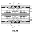
- Figure 18 shows the structure of Figure 17 following the patterning of an additional conductive layer or line (a fourth line) with conductive layer or line 298A and conductive layer or line 298B and conductive vias 297A and conductive vias 297B through the respective dielectric layers to patterned conductive layer or line 285A and 285B, respectively.
- a suitable material for patterned conductive layer or line 298A/298B and for conductive vias 297A/297B is copper deposited, for example, by an electroplating process.
- Figure 18 also shows the introduction of a dielectric material over patterned conductive layer/line 298A/298B.
- Figure 18 shows dielectric layer 299A and dielectric layer 299B on conductive layer 298A and conductive layer 298B, respectively.
- dielectric layer 296A/296B overlays on spacer layer 290A/290B
- dielectric layer 299A/299B may overlay on dielectric layer 296A/296B and spacer layer 290A/290B.
- a planarization process is performed to polish the structure to expose spacer layer 290A/290B.
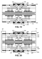
- Figure 19 shows the structure of Figure 18 following the removal of spacer layer 290A and spacer layer 290B.
- the spacer layer and conductive layer may be removed by a wet blasting process. Removal of the spacer layer proceeds to expose a portion of patterned conductive layer or line 285A and patterned conductive layer or line 285B, respectively, that was previously covered by the spacer layer. The exposed portions of patterned conductive layer or line 285A/285B will be used to connect to a secondary device (e.g., a package or die).
- a conductive material such as gold may be deposited on the exposed patterned conductive layer or line to improve an electrical connection with a secondary device.
- Figure 20 shows the structure of Figure 19 undergoing a singulation process to separate the two packages that have been described from other packages or as well as to define the xy dimensions of the two packages.
- One singulation process is by mechanical sawing. Another option is laser cutting.
- Figure 20 shows area 300 and area 305 on the left and right side, respectively, designating the area for the singulation.
- Figure 21 shows a portion of the structure of Figure 20 following the separation of the structure into two individual package portions by removal of sacrificial substrate 210 and copper foils 215A and 215B.
- Figure 21 shows a portion of a free standing microelectronic package that has a die (die 240B) connected at a device side to a build-up carrier including a number of alternating layers of electrically conductive material (four levels of conductive traces) and dielectric or insulating material.
- Figure 21 also shows the portion of the structure following the removal of spacer layer 230B and dielectric layer 225B (see, for example, Figure 7 and the associated text).
- spacer layer 230B of copper and dielectric layer 225B of ABF is by a wet blast process.
- the removal of the spacer layer and dielectric layer proceeds to expose contact pads 235B/236B.
- Contact pads 235B/236B will be used to connect the package to a substrate such as a printed circuit board.
- Figure 22 shows the package of Figure 21 inverted.
- the package is connected to substrate 325 that is, for example, a printed circuit board.
- die 240B of the package is disposed at a base of the package.
- Cavity 345 is formed laterally from the die between the package and substrate 325 with contact pads 235B in the cavity.
- the package is connected to substrate 325, in this embodiment, through solder material connections (e.g., solder balls) disposed in cavity 345 at contact pads 235B.
- solder material connections e.g., solder balls
- the package includes a protruding portion including patterned conductive layer or line 298B and laterally adjacent to the protruding portion exposed contact pads of patterned conductive layer or line 285B.
- the package is connected to a secondary device.
- Secondary device 350 is, for example, a package including a die or dice such as memory dice or other die (e.g., processor, system on a chip). With secondary device 350 disposed on the package, cavity 370 is created with contact pads of patterned conductive layer or line 285B in the cavity.
- the package is connected to secondary device 350 through solder material connections 320 (e.g., solder balls) disposed in cavity 370 at the contact pads of patterned conductive layer or line 285B.
- FIG 22 shows POP device integration assembly or apparatus where embedded die 240B (e.g., a microprocessor) is connected to the base package (a BBUL package) through bottom or first conductive layer or line 275B (L1).
- embedded die 240B is electrically connected to package 350 (e.g., a package including one or more memory devices) through conductive layers of the base package (e.g., 275B (L1), 280B (L2)) and POP pads at conductive layer 285B (L3).
- Die 240B is also electrically connected to input/output (I/O) devices on substrate 325 through vias 265B.
- I/O input/output
- the described configuration provides reduced interconnect routing between die 240B and package 350 and I/O devices of substrate 325 than previous POP assembly configurations. Reduced communication latency between devices and lower power consumption can be realized with the described configuration. Still further, the configuration utilizes conductive layer 298B (L4) effectively by incorporating routing and contact points or pads in the level.
- the dual-sided cavity design of the base package reduces the overall POP assembly thickness (z-height) with a potential to achieve greater than 25 percent base package z-height reduction over, for example, a POP assembly that might include only a single cavity between the base package and a secondary package (e.g., a POP assembly that only includes cavity 370).
- dimensions shown in Figure 22 include:
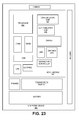
- FIG. 23 illustrates a computing device 400 in accordance with one implementation.
- Computing device 400 houses board 402.
- Board 402 may include a number of components, including but not limited to processor 404 and at least one communication chip 406.
- Processor 404 is physically and electrically connected to board 402.
- the at least one communication chip 406 is also physically and electrically connected to board 402.
- communication chip 406 is part of processor 404.
- computing device 400 may include other components that may or may not be physically and electrically connected to board 402. These other components include, but are not limited to, volatile memory (e.g., DRAM), non-volatile memory (e.g., ROM), flash memory, a graphics processor, a digital signal processor, a crypto processor, a chipset, an antenna, a display, a touchscreen display, a touchscreen controller, a battery, an audio codec, a video codec, a power amplifier, a global positioning system (GPS) device, a compass, an accelerometer, a gyroscope, a speaker, a camera, and a mass storage device (such as hard disk drive, compact disk (CD), digital versatile disk (DVD), and so forth).
- volatile memory e.g., DRAM
- non-volatile memory e.g., ROM
- flash memory e.g., a graphics processor, a digital signal processor, a crypto processor, a chipset, an antenna, a display
- Communication chip 406 enables wireless communications for the transfer of data to and from computing device 400.
- wireless and its derivatives may be used to describe circuits, devices, systems, methods, techniques, communications channels, etc., that may communicate data through the use of modulated electromagnetic radiation through a non-solid medium. The term does not imply that the associated devices do not contain any wires, although in some embodiments they might not.
- Communication chip 406 may implement any of a number of wireless standards or protocols, including but not limited to Wi-Fi (IEEE 802.11 family), WiMAX (IEEE 802.16 family), IEEE 802.20, long term evolution (LTE), Ev-DO, HSPA+, HSDPA+, HSUPA+, EDGE, GSM, GPRS, CDMA, TDMA, DECT, Bluetooth, derivatives thereof, as well as any other wireless protocols that are designated as 3G, 4G, 5G, and beyond.
- Computing device 400 may include a plurality of communication chips 406.
- a first communication chip 406 may be dedicated to shorter range wireless communications such as Wi-Fi and Bluetooth and a second communication chip 406 may be dedicated to longer range wireless communications such as GPS, EDGE, GPRS, CDMA, WiMAX, LTE, Ev-DO, and others.
- Processor 404 of computing device 400 includes an integrated circuit die packaged within processor 404.
- the package formed in accordance with embodiment described above utilizes BBUL technology with a carrier as described including a die embedded therein in at a base of the carrier body and a cavity formed between the carrier and board 402 where electrical connections are made to the board (through, for example, solder material contacts).
- the term "processor” may refer to any device or portion of a device that processes electronic data from registers and/or memory to transform that electronic data into other electronic data that may be stored in registers and/or memory.
- Communication chip 406 also includes an integrated circuit die packaged within communication chip 406.
- package is based on BBUL technology such as described above that enables stacking at a reduced z-height of various devices, including but not limited to, a microprocessor chip (die) with a memory die with a graphics die with a chip set with GPS.
- die microprocessor chip
- Such package includes the dual-sided cavity confirmation described above.
- another component housed within computing device 400 may contain a microelectronic package that incorporates a primary BBUL carrier implementation such as described above.
- computing device 400 may be a laptop, a netbook, a notebook, an ultrabook, a smartphone, a tablet, a personal digital assistant (PDA), an ultra mobile PC, a mobile phone, a desktop computer, a server, a printer, a scanner, a monitor, a set-top box, an entertainment control unit, a digital camera, a portable music player, or a digital video recorder.
- computing device 400 may be any other electronic device that processes data.
- Example 1 is an apparatus including a die having a thickness dimension and a die area defined by a length dimension and a width dimension; and a build-up carrier having a carrier area greater than the die area, the build-up carrier including a plurality of alternating layers of conductive material and dielectric material disposed on a device side of the die and dielectric material embedding a portion of the thickness dimension of the die; and a plurality of carrier contact points configured for mounting the build-up carrier to a substrate, the plurality of carrier contact points disposed at a gradation between the device side of the die and the embedded the thickness dimension of the die wherein at least one of the plurality of carrier contact points is coupled to at least one of the alternating layers of conductive materials.
- the plurality of carrier contact points of the apparatus of Example 1 include a first plurality of carrier contact points and the gradation includes a first gradation and a plurality of the layers of conductive material include an ultimate layer disposed furthest from the die, the carrier further includes a plurality of second carrier contact points disposed at a second gradation between the ultimate layer of conductive material and the die.
- Example 3 the second gradation in the apparatus of Example 2 is in a plane defined by a penultimate layer of the plurality of layers of conductive material.
- the die of the apparatus of Example 1 includes contact points on a device side and at least one of the plurality of layers of conductive material is coupled to at least one of the contact points of the die.
- Example 6 the second carrier contact points of the apparatus of Example 2 are configured for connection of the build-up carrier to a secondary device or package.
- the die of the apparatus of Example 1 includes a dielectric layer on a side opposite the device side.
- Example 8 is a method including disposing a die on a sacrificial substrate with a device side of the die opposite the sacrificial substrate; forming a build-up carrier adjacent a device side of a die, wherein the build-up carrier includes a plurality of alternating layers of conductive material and dielectric material, and dielectric material embedding a portion of a thickness dimension of the die and defining a gradation between the device side of the die and a backside of the die, the gradation including a plurality of carrier contact points configured for mounting the build-up carrier to the substrate; and separating the die and the build-up carrier from the sacrificial substrate.
- Example 9 prior to forming the build-up carrier in the method of Example 8, the method includes disposing a spacer layer on the sacrificial substrate, the spacer layer including an opening to accomodate the die on the sacrificial substrate and dielectric material to embed a portion of the thickness dimension of the die, the spacer layer having a thickness equivalent to a thickness of the first gradation, and after forming the build-up carrier, separating the die and the build-up carrier from the sacrificial substrate includes separating from the spacer layer.
- forming the build-up carrier in the method of Example 9 includes forming the plurality of carrier contact points on the spacer layer.
- Example 11 the plurality of carrier contact points in the method of Example 10 are configured for connection of the build-up carrier to a printed circuit board.
- the gradation in the method of Example 8 includes a first gradation and forming the build-up carrier includes patterning the penultimate layer of the plurality of conductive layers and forming a spacer layer on the patterned penultimate layer, the spacer layer including an opening to accomodate the ultimate layer of the plurality of conductive layers, the spacer layer having a thickness equivalent to a thickness of a second gradation; and patterning the ultimate layer of the plurality of conductive layers, and after forming the build-up carrier, removing the spacer layer.
- forming the build-up carrier in the method of Example 11 includes disposing dielectric material on the patterned ultimate layer of the plurality of conductive layers.
- patterning the penultimate layer of the plurality of conductive layers in the method of Example 12 includes patterning the penultimate layer into the second plurality of carrier contact points configured for connection of the build-up carrier to a secondary device or package.
- Example 15 any of the methods of Examples 8-14 are used in the formation of a package including at least one die (e.g., an integrated circuit substrate).
- Example 16 includes a package including a microprocessor disposed in a carrier, the microprocessor including a first side and an opposite second side including a device side with contact points and a microprocessor area defined by a length dimension and a width dimension; the carrier including a carrier area greater than the microprocessor area; a plurality of alternating layers of conductive material and dielectric material disposed on the second side of the microprocessor with, of a plurality of the layers of conductive material, an ultimate layer of conductive material disposed furthest from the microprocessor and with dielectric material embedding a portion of a thickness dimension of the microprocessor; a plurality of first carrier contact points disposed at a first gradation between the second side of the microprocessor and the dielectric material embedding the thickness dimension of the microprocessor; and a plurality of second carrier contact points disposed at a second gradation between the ultimate layer of conductive material and the microprocessor; and a printed circuit board coupled to the first carrier contact points.
- Example 17 the apparatus of Example 16 further includes a secondary device or package coupled to the second carrier contact points.
- the second gradation of the apparatus of Example 16 includes a thickness dimension equivalent to a separation between the ultimate layer of conductive material and a penultimate layer of the plurality of layers of conductive material.
Landscapes
- Production Of Multi-Layered Print Wiring Board (AREA)
- Engineering & Computer Science (AREA)
- Ceramic Engineering (AREA)
- Manufacturing & Machinery (AREA)
Applications Claiming Priority (1)
| Application Number | Priority Date | Filing Date | Title |
|---|---|---|---|
| US13/852,876 US9455218B2 (en) | 2013-03-28 | 2013-03-28 | Embedded die-down package-on-package device |
Publications (2)
| Publication Number | Publication Date |
|---|---|
| EP2816596A1 true EP2816596A1 (de) | 2014-12-24 |
| EP2816596B1 EP2816596B1 (de) | 2020-07-15 |
Family
ID=50336229
Family Applications (1)
| Application Number | Title | Priority Date | Filing Date |
|---|---|---|---|
| EP14161193.9A Active EP2816596B1 (de) | 2013-03-28 | 2014-03-21 | Eingebettetes Die-Down-Paket mit Paket-auf-Paket-Vorrichtung |
Country Status (5)
| Country | Link |
|---|---|
| US (2) | US9455218B2 (de) |
| EP (1) | EP2816596B1 (de) |
| JP (1) | JP5889947B2 (de) |
| KR (2) | KR101594384B1 (de) |
| CN (1) | CN104078453B (de) |
Families Citing this family (33)
| Publication number | Priority date | Publication date | Assignee | Title |
|---|---|---|---|---|
| US20150282367A1 (en) * | 2014-03-27 | 2015-10-01 | Hans-Joachim Barth | Electronic assembly that includes stacked electronic components |
| US9930793B2 (en) * | 2014-03-27 | 2018-03-27 | Intel Corporation | Electric circuit on flexible substrate |
| US9401350B1 (en) * | 2015-07-29 | 2016-07-26 | Qualcomm Incorporated | Package-on-package (POP) structure including multiple dies |
| US9711458B2 (en) * | 2015-11-13 | 2017-07-18 | Taiwan Semiconductor Manufacturing Company, Ltd. | Structure and formation method for chip package |
| EP3255665B1 (de) * | 2016-06-08 | 2022-01-12 | AT & S Austria Technologie & Systemtechnik Aktiengesellschaft | Elektronisches bauteil mit komponententräger und seine herstellung |
| EP3302006A1 (de) | 2016-09-30 | 2018-04-04 | AT & S Austria Technologie & Systemtechnik Aktiengesellschaft | Komponententräger mit mindestens einem wärmerohr und verfahren zur herstellung des besagten komponententrägers |
| SG10201608773PA (en) * | 2016-10-19 | 2018-05-30 | Delta Electronics Intl Singapore Pte Ltd | Method Of Packaging Semiconductor Device |
| TW202537391A (zh) | 2016-12-14 | 2025-09-16 | 成真股份有限公司 | 標準大宗商品化現場可編程邏輯閘陣列(fpga)積體電路晶片組成之邏輯驅動器 |
| US11625523B2 (en) | 2016-12-14 | 2023-04-11 | iCometrue Company Ltd. | Logic drive based on standard commodity FPGA IC chips |
| CN107123604A (zh) * | 2017-06-01 | 2017-09-01 | 中芯长电半导体(江阴)有限公司 | 一种双面成型的封装方法 |
| US10447274B2 (en) | 2017-07-11 | 2019-10-15 | iCometrue Company Ltd. | Logic drive based on standard commodity FPGA IC chips using non-volatile memory cells |
| US10993333B2 (en) * | 2017-07-15 | 2021-04-27 | Sanmina Corporation | Methods of manufacturing ultra thin dielectric printed circuit boards with thin laminates |
| US10957679B2 (en) | 2017-08-08 | 2021-03-23 | iCometrue Company Ltd. | Logic drive based on standardized commodity programmable logic semiconductor IC chips |
| US10630296B2 (en) | 2017-09-12 | 2020-04-21 | iCometrue Company Ltd. | Logic drive with brain-like elasticity and integrality based on standard commodity FPGA IC chips using non-volatile memory cells |
| US10504865B2 (en) * | 2017-09-28 | 2019-12-10 | Taiwan Semiconductor Manufacturing Co., Ltd. | Package structure and method of manufacturing the same |
| US10608642B2 (en) | 2018-02-01 | 2020-03-31 | iCometrue Company Ltd. | Logic drive using standard commodity programmable logic IC chips comprising non-volatile radom access memory cells |
| US10623000B2 (en) | 2018-02-14 | 2020-04-14 | iCometrue Company Ltd. | Logic drive using standard commodity programmable logic IC chips |
| US12476637B2 (en) | 2018-05-24 | 2025-11-18 | iCometrue Company Ltd. | Logic drive using standard commodity programmable logic IC chips |
| US10608638B2 (en) | 2018-05-24 | 2020-03-31 | iCometrue Company Ltd. | Logic drive using standard commodity programmable logic IC chips |
| US11309334B2 (en) | 2018-09-11 | 2022-04-19 | iCometrue Company Ltd. | Logic drive using standard commodity programmable logic IC chips comprising non-volatile random access memory cells |
| US10937762B2 (en) | 2018-10-04 | 2021-03-02 | iCometrue Company Ltd. | Logic drive based on multichip package using interconnection bridge |
| US11616046B2 (en) | 2018-11-02 | 2023-03-28 | iCometrue Company Ltd. | Logic drive based on chip scale package comprising standardized commodity programmable logic IC chip and memory IC chip |
| US11211334B2 (en) | 2018-11-18 | 2021-12-28 | iCometrue Company Ltd. | Logic drive based on chip scale package comprising standardized commodity programmable logic IC chip and memory IC chip |
| US11658122B2 (en) | 2019-03-18 | 2023-05-23 | Intel Corporation | EMIB patch on glass laminate substrate |
| US11227838B2 (en) | 2019-07-02 | 2022-01-18 | iCometrue Company Ltd. | Logic drive based on multichip package comprising standard commodity FPGA IC chip with cooperating or supporting circuits |
| US11887930B2 (en) | 2019-08-05 | 2024-01-30 | iCometrue Company Ltd. | Vertical interconnect elevator based on through silicon vias |
| US11637056B2 (en) | 2019-09-20 | 2023-04-25 | iCometrue Company Ltd. | 3D chip package based on through-silicon-via interconnection elevator |
| US11600526B2 (en) | 2020-01-22 | 2023-03-07 | iCometrue Company Ltd. | Chip package based on through-silicon-via connector and silicon interconnection bridge |
| TW202240808A (zh) | 2021-01-08 | 2022-10-16 | 成真股份有限公司 | 使用於積體電路晶片封裝結構中的微型熱導管 |
| JP7676800B2 (ja) * | 2021-02-15 | 2025-05-15 | Toppanホールディングス株式会社 | 配線基板積層体 |
| US12176278B2 (en) | 2021-05-30 | 2024-12-24 | iCometrue Company Ltd. | 3D chip package based on vertical-through-via connector |
| US20230187365A1 (en) | 2021-09-24 | 2023-06-15 | iCometrue Company Ltd. | Field Programmable Multichip Package Based on Field-Programmable-Gate-Array (FPGA) Integrated-Circuit (IC) Chip |
| US12268012B2 (en) | 2021-09-24 | 2025-04-01 | iCometrue Company Ltd. | Multi-output look-up table (LUT) for use in coarse-grained field-programmable-gate-array (FPGA) integrated-circuit (IC) chip |
Citations (2)
| Publication number | Priority date | Publication date | Assignee | Title |
|---|---|---|---|---|
| US20060134835A1 (en) * | 2002-11-06 | 2006-06-22 | Sambo He | Method for making a neo-layer comprising embedded discrete components |
| US20130026653A1 (en) * | 2010-03-23 | 2013-01-31 | Nec Corporation | Method for manufacturing semiconductor device |
Family Cites Families (13)
| Publication number | Priority date | Publication date | Assignee | Title |
|---|---|---|---|---|
| US6515355B1 (en) * | 1998-09-02 | 2003-02-04 | Micron Technology, Inc. | Passivation layer for packaged integrated circuits |
| US20020124955A1 (en) * | 2001-03-08 | 2002-09-12 | I-Chung Tung | Attachment of a heat spreader for fabricating a cavity down plastic chip carrier |
| US6992899B2 (en) | 2003-03-21 | 2006-01-31 | Intel Corporation | Power delivery apparatus, systems, and methods |
| JP4271590B2 (ja) | 2004-01-20 | 2009-06-03 | 新光電気工業株式会社 | 半導体装置及びその製造方法 |
| US7919844B2 (en) * | 2005-05-26 | 2011-04-05 | Aprolase Development Co., Llc | Tier structure with tier frame having a feedthrough structure |
| JP2009135391A (ja) | 2007-11-02 | 2009-06-18 | Denso Corp | 電子装置およびその製造方法 |
| US20100073894A1 (en) | 2008-09-22 | 2010-03-25 | Russell Mortensen | Coreless substrate, method of manufacturing same, and package for microelectronic device incorporating same |
| KR101058621B1 (ko) | 2009-07-23 | 2011-08-22 | 삼성전기주식회사 | 반도체 패키지 및 이의 제조 방법 |
| JP5249173B2 (ja) | 2009-10-30 | 2013-07-31 | 新光電気工業株式会社 | 半導体素子実装配線基板及びその製造方法 |
| US8716873B2 (en) * | 2010-07-01 | 2014-05-06 | United Test And Assembly Center Ltd. | Semiconductor packages and methods of packaging semiconductor devices |
| US20120319295A1 (en) * | 2011-06-17 | 2012-12-20 | Chi Heejo | Integrated circuit packaging system with pads and method of manufacture thereof |
| US8916481B2 (en) * | 2011-11-02 | 2014-12-23 | Stmicroelectronics Pte Ltd. | Embedded wafer level package for 3D and package-on-package applications, and method of manufacture |
| US9721878B2 (en) * | 2012-09-28 | 2017-08-01 | Intel Corporation | High density second level interconnection for bumpless build up layer (BBUL) packaging technology |
-
2013
- 2013-03-28 US US13/852,876 patent/US9455218B2/en not_active Expired - Fee Related
-
2014
- 2014-03-21 EP EP14161193.9A patent/EP2816596B1/de active Active
- 2014-03-27 CN CN201410267110.4A patent/CN104078453B/zh active Active
- 2014-03-27 KR KR1020140035901A patent/KR101594384B1/ko active Active
- 2014-03-28 JP JP2014069161A patent/JP5889947B2/ja not_active Expired - Fee Related
-
2015
- 2015-07-15 KR KR1020150100666A patent/KR20150088231A/ko not_active Withdrawn
-
2016
- 2016-09-22 US US15/273,549 patent/US9812422B2/en not_active Expired - Fee Related
Patent Citations (2)
| Publication number | Priority date | Publication date | Assignee | Title |
|---|---|---|---|---|
| US20060134835A1 (en) * | 2002-11-06 | 2006-06-22 | Sambo He | Method for making a neo-layer comprising embedded discrete components |
| US20130026653A1 (en) * | 2010-03-23 | 2013-01-31 | Nec Corporation | Method for manufacturing semiconductor device |
Also Published As
| Publication number | Publication date |
|---|---|
| JP5889947B2 (ja) | 2016-03-22 |
| CN104078453A (zh) | 2014-10-01 |
| KR20140119636A (ko) | 2014-10-10 |
| KR101594384B1 (ko) | 2016-02-16 |
| US20140291866A1 (en) | 2014-10-02 |
| US20170012020A1 (en) | 2017-01-12 |
| JP2014195076A (ja) | 2014-10-09 |
| CN104078453B (zh) | 2017-04-12 |
| US9455218B2 (en) | 2016-09-27 |
| EP2816596B1 (de) | 2020-07-15 |
| KR20150088231A (ko) | 2015-07-31 |
| US9812422B2 (en) | 2017-11-07 |
Similar Documents
| Publication | Publication Date | Title |
|---|---|---|
| EP2816596B1 (de) | Eingebettetes Die-Down-Paket mit Paket-auf-Paket-Vorrichtung | |
| US9806050B2 (en) | Method of fabricating package structure | |
| TWI705611B (zh) | 天線基底以及包括其的天線模組 | |
| US9691728B2 (en) | BBUL top side substrate layer enabling dual sided silicon interconnect and stacking flexibility | |
| KR101652890B1 (ko) | 빌드업층에 임베드된 로직 다이 및 다른 컴포넌트 | |
| US9721878B2 (en) | High density second level interconnection for bumpless build up layer (BBUL) packaging technology | |
| US10483197B2 (en) | Semiconductor package | |
| US9159714B2 (en) | Package on wide I/O silicon | |
| US11049782B2 (en) | Fan-out semiconductor package | |
| US9601421B2 (en) | BBUL material integration in-plane with embedded die for warpage control | |
| KR102952166B1 (ko) | 초박형 브리지 및 멀티-다이 초미세 피치 패치 아키텍처 및 제조 방법 | |
| US20210343659A1 (en) | Fan-out semiconductor package | |
| TW201246499A (en) | A multi-chip package having a substrate with a plurality of vertically embedded die and a process forming the same | |
| US20130313727A1 (en) | Multi-stacked bbul package | |
| TWI734962B (zh) | 半導體封裝與包括其的天線模組 | |
| US9041207B2 (en) | Method to increase I/O density and reduce layer counts in BBUL packages | |
| US11640952B2 (en) | Electronic component embedded substrate | |
| US12526930B2 (en) | Printed circuit board and method of manufacturing the same | |
| KR20140076089A (ko) | 반도체 기판 및 그 제조 방법, 그리고 반도체 패키지 |
Legal Events
| Date | Code | Title | Description |
|---|---|---|---|
| PUAI | Public reference made under article 153(3) epc to a published international application that has entered the european phase |
Free format text: ORIGINAL CODE: 0009012 |
|
| 17P | Request for examination filed |
Effective date: 20140321 |
|
| AK | Designated contracting states |
Kind code of ref document: A1 Designated state(s): AL AT BE BG CH CY CZ DE DK EE ES FI FR GB GR HR HU IE IS IT LI LT LU LV MC MK MT NL NO PL PT RO RS SE SI SK SM TR |
|
| AX | Request for extension of the european patent |
Extension state: BA ME |
|
| 17Q | First examination report despatched |
Effective date: 20141217 |
|
| RBV | Designated contracting states (corrected) |
Designated state(s): AL AT BE BG CH CY CZ DE DK EE ES FI FR GB GR HR HU IE IS IT LI LT LU LV MC MK MT NL NO PL PT RO RS SE SI SK SM TR |
|
| STAA | Information on the status of an ep patent application or granted ep patent |
Free format text: STATUS: EXAMINATION IS IN PROGRESS |
|
| GRAP | Despatch of communication of intention to grant a patent |
Free format text: ORIGINAL CODE: EPIDOSNIGR1 |
|
| STAA | Information on the status of an ep patent application or granted ep patent |
Free format text: STATUS: GRANT OF PATENT IS INTENDED |
|
| INTG | Intention to grant announced |
Effective date: 20200207 |
|
| GRAS | Grant fee paid |
Free format text: ORIGINAL CODE: EPIDOSNIGR3 |
|
| GRAA | (expected) grant |
Free format text: ORIGINAL CODE: 0009210 |
|
| STAA | Information on the status of an ep patent application or granted ep patent |
Free format text: STATUS: THE PATENT HAS BEEN GRANTED |
|
| AK | Designated contracting states |
Kind code of ref document: B1 Designated state(s): AL AT BE BG CH CY CZ DE DK EE ES FI FR GB GR HR HU IE IS IT LI LT LU LV MC MK MT NL NO PL PT RO RS SE SI SK SM TR |
|
| REG | Reference to a national code |
Ref country code: GB Ref legal event code: FG4D Ref country code: CH Ref legal event code: EP |
|
| REG | Reference to a national code |
Ref country code: IE Ref legal event code: FG4D |
|
| REG | Reference to a national code |
Ref country code: DE Ref legal event code: R096 Ref document number: 602014067662 Country of ref document: DE |
|
| REG | Reference to a national code |
Ref country code: AT Ref legal event code: REF Ref document number: 1291940 Country of ref document: AT Kind code of ref document: T Effective date: 20200815 |
|
| REG | Reference to a national code |
Ref country code: NL Ref legal event code: FP |
|
| REG | Reference to a national code |
Ref country code: LT Ref legal event code: MG4D |
|
| REG | Reference to a national code |
Ref country code: AT Ref legal event code: MK05 Ref document number: 1291940 Country of ref document: AT Kind code of ref document: T Effective date: 20200715 |
|
| PG25 | Lapsed in a contracting state [announced via postgrant information from national office to epo] |
Ref country code: BG Free format text: LAPSE BECAUSE OF FAILURE TO SUBMIT A TRANSLATION OF THE DESCRIPTION OR TO PAY THE FEE WITHIN THE PRESCRIBED TIME-LIMIT Effective date: 20201015 Ref country code: ES Free format text: LAPSE BECAUSE OF FAILURE TO SUBMIT A TRANSLATION OF THE DESCRIPTION OR TO PAY THE FEE WITHIN THE PRESCRIBED TIME-LIMIT Effective date: 20200715 Ref country code: NO Free format text: LAPSE BECAUSE OF FAILURE TO SUBMIT A TRANSLATION OF THE DESCRIPTION OR TO PAY THE FEE WITHIN THE PRESCRIBED TIME-LIMIT Effective date: 20201015 Ref country code: GR Free format text: LAPSE BECAUSE OF FAILURE TO SUBMIT A TRANSLATION OF THE DESCRIPTION OR TO PAY THE FEE WITHIN THE PRESCRIBED TIME-LIMIT Effective date: 20201016 Ref country code: HR Free format text: LAPSE BECAUSE OF FAILURE TO SUBMIT A TRANSLATION OF THE DESCRIPTION OR TO PAY THE FEE WITHIN THE PRESCRIBED TIME-LIMIT Effective date: 20200715 Ref country code: AT Free format text: LAPSE BECAUSE OF FAILURE TO SUBMIT A TRANSLATION OF THE DESCRIPTION OR TO PAY THE FEE WITHIN THE PRESCRIBED TIME-LIMIT Effective date: 20200715 Ref country code: LT Free format text: LAPSE BECAUSE OF FAILURE TO SUBMIT A TRANSLATION OF THE DESCRIPTION OR TO PAY THE FEE WITHIN THE PRESCRIBED TIME-LIMIT Effective date: 20200715 Ref country code: PT Free format text: LAPSE BECAUSE OF FAILURE TO SUBMIT A TRANSLATION OF THE DESCRIPTION OR TO PAY THE FEE WITHIN THE PRESCRIBED TIME-LIMIT Effective date: 20201116 Ref country code: SE Free format text: LAPSE BECAUSE OF FAILURE TO SUBMIT A TRANSLATION OF THE DESCRIPTION OR TO PAY THE FEE WITHIN THE PRESCRIBED TIME-LIMIT Effective date: 20200715 Ref country code: FI Free format text: LAPSE BECAUSE OF FAILURE TO SUBMIT A TRANSLATION OF THE DESCRIPTION OR TO PAY THE FEE WITHIN THE PRESCRIBED TIME-LIMIT Effective date: 20200715 |
|
| PG25 | Lapsed in a contracting state [announced via postgrant information from national office to epo] |
Ref country code: IS Free format text: LAPSE BECAUSE OF FAILURE TO SUBMIT A TRANSLATION OF THE DESCRIPTION OR TO PAY THE FEE WITHIN THE PRESCRIBED TIME-LIMIT Effective date: 20201115 Ref country code: PL Free format text: LAPSE BECAUSE OF FAILURE TO SUBMIT A TRANSLATION OF THE DESCRIPTION OR TO PAY THE FEE WITHIN THE PRESCRIBED TIME-LIMIT Effective date: 20200715 Ref country code: RS Free format text: LAPSE BECAUSE OF FAILURE TO SUBMIT A TRANSLATION OF THE DESCRIPTION OR TO PAY THE FEE WITHIN THE PRESCRIBED TIME-LIMIT Effective date: 20200715 Ref country code: LV Free format text: LAPSE BECAUSE OF FAILURE TO SUBMIT A TRANSLATION OF THE DESCRIPTION OR TO PAY THE FEE WITHIN THE PRESCRIBED TIME-LIMIT Effective date: 20200715 |
|
| REG | Reference to a national code |
Ref country code: DE Ref legal event code: R097 Ref document number: 602014067662 Country of ref document: DE |
|
| PG25 | Lapsed in a contracting state [announced via postgrant information from national office to epo] |
Ref country code: RO Free format text: LAPSE BECAUSE OF FAILURE TO SUBMIT A TRANSLATION OF THE DESCRIPTION OR TO PAY THE FEE WITHIN THE PRESCRIBED TIME-LIMIT Effective date: 20200715 Ref country code: SM Free format text: LAPSE BECAUSE OF FAILURE TO SUBMIT A TRANSLATION OF THE DESCRIPTION OR TO PAY THE FEE WITHIN THE PRESCRIBED TIME-LIMIT Effective date: 20200715 Ref country code: IT Free format text: LAPSE BECAUSE OF FAILURE TO SUBMIT A TRANSLATION OF THE DESCRIPTION OR TO PAY THE FEE WITHIN THE PRESCRIBED TIME-LIMIT Effective date: 20200715 Ref country code: DK Free format text: LAPSE BECAUSE OF FAILURE TO SUBMIT A TRANSLATION OF THE DESCRIPTION OR TO PAY THE FEE WITHIN THE PRESCRIBED TIME-LIMIT Effective date: 20200715 Ref country code: EE Free format text: LAPSE BECAUSE OF FAILURE TO SUBMIT A TRANSLATION OF THE DESCRIPTION OR TO PAY THE FEE WITHIN THE PRESCRIBED TIME-LIMIT Effective date: 20200715 Ref country code: CZ Free format text: LAPSE BECAUSE OF FAILURE TO SUBMIT A TRANSLATION OF THE DESCRIPTION OR TO PAY THE FEE WITHIN THE PRESCRIBED TIME-LIMIT Effective date: 20200715 |
|
| PLBE | No opposition filed within time limit |
Free format text: ORIGINAL CODE: 0009261 |
|
| STAA | Information on the status of an ep patent application or granted ep patent |
Free format text: STATUS: NO OPPOSITION FILED WITHIN TIME LIMIT |
|
| PG25 | Lapsed in a contracting state [announced via postgrant information from national office to epo] |
Ref country code: AL Free format text: LAPSE BECAUSE OF FAILURE TO SUBMIT A TRANSLATION OF THE DESCRIPTION OR TO PAY THE FEE WITHIN THE PRESCRIBED TIME-LIMIT Effective date: 20200715 |
|
| 26N | No opposition filed |
Effective date: 20210416 |
|
| PG25 | Lapsed in a contracting state [announced via postgrant information from national office to epo] |
Ref country code: SK Free format text: LAPSE BECAUSE OF FAILURE TO SUBMIT A TRANSLATION OF THE DESCRIPTION OR TO PAY THE FEE WITHIN THE PRESCRIBED TIME-LIMIT Effective date: 20200715 |
|
| PG25 | Lapsed in a contracting state [announced via postgrant information from national office to epo] |
Ref country code: SI Free format text: LAPSE BECAUSE OF FAILURE TO SUBMIT A TRANSLATION OF THE DESCRIPTION OR TO PAY THE FEE WITHIN THE PRESCRIBED TIME-LIMIT Effective date: 20200715 |
|
| PG25 | Lapsed in a contracting state [announced via postgrant information from national office to epo] |
Ref country code: MC Free format text: LAPSE BECAUSE OF FAILURE TO SUBMIT A TRANSLATION OF THE DESCRIPTION OR TO PAY THE FEE WITHIN THE PRESCRIBED TIME-LIMIT Effective date: 20200715 |
|
| REG | Reference to a national code |
Ref country code: CH Ref legal event code: PL |
|
| REG | Reference to a national code |
Ref country code: BE Ref legal event code: MM Effective date: 20210331 |
|
| PG25 | Lapsed in a contracting state [announced via postgrant information from national office to epo] |
Ref country code: CH Free format text: LAPSE BECAUSE OF NON-PAYMENT OF DUE FEES Effective date: 20210331 Ref country code: LU Free format text: LAPSE BECAUSE OF NON-PAYMENT OF DUE FEES Effective date: 20210321 Ref country code: LI Free format text: LAPSE BECAUSE OF NON-PAYMENT OF DUE FEES Effective date: 20210331 Ref country code: IE Free format text: LAPSE BECAUSE OF NON-PAYMENT OF DUE FEES Effective date: 20210321 |
|
| PG25 | Lapsed in a contracting state [announced via postgrant information from national office to epo] |
Ref country code: BE Free format text: LAPSE BECAUSE OF NON-PAYMENT OF DUE FEES Effective date: 20210331 |
|
| PG25 | Lapsed in a contracting state [announced via postgrant information from national office to epo] |
Ref country code: HU Free format text: LAPSE BECAUSE OF FAILURE TO SUBMIT A TRANSLATION OF THE DESCRIPTION OR TO PAY THE FEE WITHIN THE PRESCRIBED TIME-LIMIT; INVALID AB INITIO Effective date: 20140321 |
|
| P01 | Opt-out of the competence of the unified patent court (upc) registered |
Effective date: 20230518 |
|
| PG25 | Lapsed in a contracting state [announced via postgrant information from national office to epo] |
Ref country code: CY Free format text: LAPSE BECAUSE OF FAILURE TO SUBMIT A TRANSLATION OF THE DESCRIPTION OR TO PAY THE FEE WITHIN THE PRESCRIBED TIME-LIMIT Effective date: 20200715 |
|
| PG25 | Lapsed in a contracting state [announced via postgrant information from national office to epo] |
Ref country code: MK Free format text: LAPSE BECAUSE OF FAILURE TO SUBMIT A TRANSLATION OF THE DESCRIPTION OR TO PAY THE FEE WITHIN THE PRESCRIBED TIME-LIMIT Effective date: 20200715 |
|
| PG25 | Lapsed in a contracting state [announced via postgrant information from national office to epo] |
Ref country code: MT Free format text: LAPSE BECAUSE OF FAILURE TO SUBMIT A TRANSLATION OF THE DESCRIPTION OR TO PAY THE FEE WITHIN THE PRESCRIBED TIME-LIMIT Effective date: 20200715 |
|
| REG | Reference to a national code |
Ref country code: DE Ref legal event code: R079 Ref document number: 602014067662 Country of ref document: DE Free format text: PREVIOUS MAIN CLASS: H01L0023480000 Ipc: H10W0072000000 |
|
| PG25 | Lapsed in a contracting state [announced via postgrant information from national office to epo] |
Ref country code: TR Free format text: LAPSE BECAUSE OF FAILURE TO SUBMIT A TRANSLATION OF THE DESCRIPTION OR TO PAY THE FEE WITHIN THE PRESCRIBED TIME-LIMIT Effective date: 20200715 |
|
| PGFP | Annual fee paid to national office [announced via postgrant information from national office to epo] |
Ref country code: NL Payment date: 20260227 Year of fee payment: 13 |
|
| PGFP | Annual fee paid to national office [announced via postgrant information from national office to epo] |
Ref country code: GB Payment date: 20260223 Year of fee payment: 13 |
|
| PGFP | Annual fee paid to national office [announced via postgrant information from national office to epo] |
Ref country code: DE Payment date: 20260102 Year of fee payment: 13 |
|
| PGFP | Annual fee paid to national office [announced via postgrant information from national office to epo] |
Ref country code: FR Payment date: 20260223 Year of fee payment: 13 |