EP2812919B1 - Ensemble de puces empilées avec plusieurs interposeurs - Google Patents
Ensemble de puces empilées avec plusieurs interposeurs Download PDFInfo
- Publication number
- EP2812919B1 EP2812919B1 EP12816386.2A EP12816386A EP2812919B1 EP 2812919 B1 EP2812919 B1 EP 2812919B1 EP 12816386 A EP12816386 A EP 12816386A EP 2812919 B1 EP2812919 B1 EP 2812919B1
- Authority
- EP
- European Patent Office
- Prior art keywords
- interposer
- die
- interconnect
- integrated circuit
- interconnects
- Prior art date
- Legal status (The legal status is an assumption and is not a legal conclusion. Google has not performed a legal analysis and makes no representation as to the accuracy of the status listed.)
- Active
Links
- 239000000758 substrate Substances 0.000 claims description 48
- 230000006854 communication Effects 0.000 claims description 23
- 238000004891 communication Methods 0.000 claims description 23
- 238000000034 method Methods 0.000 claims description 19
- 229910052751 metal Inorganic materials 0.000 claims description 12
- 239000002184 metal Substances 0.000 claims description 12
- 239000011295 pitch Substances 0.000 description 64
- 229910000679 solder Inorganic materials 0.000 description 56
- 238000010586 diagram Methods 0.000 description 47
- 235000012431 wafers Nutrition 0.000 description 28
- 238000000429 assembly Methods 0.000 description 19
- 230000000712 assembly Effects 0.000 description 19
- 229910052710 silicon Inorganic materials 0.000 description 17
- 239000010703 silicon Substances 0.000 description 17
- 238000003384 imaging method Methods 0.000 description 14
- XUIMIQQOPSSXEZ-UHFFFAOYSA-N Silicon Chemical compound [Si] XUIMIQQOPSSXEZ-UHFFFAOYSA-N 0.000 description 13
- 230000008878 coupling Effects 0.000 description 11
- 238000010168 coupling process Methods 0.000 description 11
- 238000005859 coupling reaction Methods 0.000 description 11
- 238000004549 pulsed laser deposition Methods 0.000 description 9
- 230000007175 bidirectional communication Effects 0.000 description 7
- 239000000463 material Substances 0.000 description 6
- 230000002457 bidirectional effect Effects 0.000 description 5
- 239000004020 conductor Substances 0.000 description 5
- 230000006870 function Effects 0.000 description 5
- PXHVJJICTQNCMI-UHFFFAOYSA-N Nickel Chemical compound [Ni] PXHVJJICTQNCMI-UHFFFAOYSA-N 0.000 description 4
- 235000019800 disodium phosphate Nutrition 0.000 description 4
- 239000011806 microball Substances 0.000 description 4
- 239000005022 packaging material Substances 0.000 description 4
- 230000008569 process Effects 0.000 description 4
- 238000012545 processing Methods 0.000 description 4
- 239000004065 semiconductor Substances 0.000 description 4
- 230000003139 buffering effect Effects 0.000 description 3
- 238000005520 cutting process Methods 0.000 description 3
- 238000013461 design Methods 0.000 description 3
- 229910003460 diamond Inorganic materials 0.000 description 3
- 239000010432 diamond Substances 0.000 description 3
- 238000005516 engineering process Methods 0.000 description 3
- 238000000608 laser ablation Methods 0.000 description 3
- 238000001459 lithography Methods 0.000 description 3
- 238000004806 packaging method and process Methods 0.000 description 3
- RYGMFSIKBFXOCR-UHFFFAOYSA-N Copper Chemical compound [Cu] RYGMFSIKBFXOCR-UHFFFAOYSA-N 0.000 description 2
- VYPSYNLAJGMNEJ-UHFFFAOYSA-N Silicium dioxide Chemical compound O=[Si]=O VYPSYNLAJGMNEJ-UHFFFAOYSA-N 0.000 description 2
- 229910052782 aluminium Inorganic materials 0.000 description 2
- XAGFODPZIPBFFR-UHFFFAOYSA-N aluminium Chemical compound [Al] XAGFODPZIPBFFR-UHFFFAOYSA-N 0.000 description 2
- 238000013459 approach Methods 0.000 description 2
- 239000011805 ball Substances 0.000 description 2
- 230000008901 benefit Effects 0.000 description 2
- 230000015572 biosynthetic process Effects 0.000 description 2
- 239000000872 buffer Substances 0.000 description 2
- 229910052802 copper Inorganic materials 0.000 description 2
- 239000010949 copper Substances 0.000 description 2
- 230000001419 dependent effect Effects 0.000 description 2
- 230000008021 deposition Effects 0.000 description 2
- 238000000151 deposition Methods 0.000 description 2
- 239000004744 fabric Substances 0.000 description 2
- PCHJSUWPFVWCPO-UHFFFAOYSA-N gold Chemical compound [Au] PCHJSUWPFVWCPO-UHFFFAOYSA-N 0.000 description 2
- 229910052737 gold Inorganic materials 0.000 description 2
- 239000010931 gold Substances 0.000 description 2
- 238000002370 liquid polymer infiltration Methods 0.000 description 2
- 238000004519 manufacturing process Methods 0.000 description 2
- 238000004377 microelectronic Methods 0.000 description 2
- 229910052759 nickel Inorganic materials 0.000 description 2
- 238000000926 separation method Methods 0.000 description 2
- 229910021332 silicide Inorganic materials 0.000 description 2
- 239000007787 solid Substances 0.000 description 2
- 230000003068 static effect Effects 0.000 description 2
- 101100498818 Arabidopsis thaliana DDR4 gene Proteins 0.000 description 1
- 101000822695 Clostridium perfringens (strain 13 / Type A) Small, acid-soluble spore protein C1 Proteins 0.000 description 1
- 101000655262 Clostridium perfringens (strain 13 / Type A) Small, acid-soluble spore protein C2 Proteins 0.000 description 1
- 101000655256 Paraclostridium bifermentans Small, acid-soluble spore protein alpha Proteins 0.000 description 1
- 101000655264 Paraclostridium bifermentans Small, acid-soluble spore protein beta Proteins 0.000 description 1
- 239000000853 adhesive Substances 0.000 description 1
- 230000001070 adhesive effect Effects 0.000 description 1
- 238000003491 array Methods 0.000 description 1
- 230000032798 delamination Effects 0.000 description 1
- 238000005553 drilling Methods 0.000 description 1
- 230000000694 effects Effects 0.000 description 1
- 238000005530 etching Methods 0.000 description 1
- 239000011521 glass Substances 0.000 description 1
- 239000012535 impurity Substances 0.000 description 1
- 239000011159 matrix material Substances 0.000 description 1
- 239000012778 molding material Substances 0.000 description 1
- 238000012544 monitoring process Methods 0.000 description 1
- 238000000465 moulding Methods 0.000 description 1
- 230000003287 optical effect Effects 0.000 description 1
- 238000012856 packing Methods 0.000 description 1
- 229920000747 poly(lactic acid) Polymers 0.000 description 1
- 238000007639 printing Methods 0.000 description 1
- 230000000644 propagated effect Effects 0.000 description 1
- 230000009467 reduction Effects 0.000 description 1
- 235000012239 silicon dioxide Nutrition 0.000 description 1
- 239000000377 silicon dioxide Substances 0.000 description 1
Images


Classifications
-
- H—ELECTRICITY
- H01—ELECTRIC ELEMENTS
- H01L—SEMICONDUCTOR DEVICES NOT COVERED BY CLASS H10
- H01L25/00—Assemblies consisting of a plurality of individual semiconductor or other solid state devices ; Multistep manufacturing processes thereof
- H01L25/03—Assemblies consisting of a plurality of individual semiconductor or other solid state devices ; Multistep manufacturing processes thereof all the devices being of a type provided for in the same subgroup of groups H01L27/00 - H01L33/00, or in a single subclass of H10K, H10N, e.g. assemblies of rectifier diodes
- H01L25/04—Assemblies consisting of a plurality of individual semiconductor or other solid state devices ; Multistep manufacturing processes thereof all the devices being of a type provided for in the same subgroup of groups H01L27/00 - H01L33/00, or in a single subclass of H10K, H10N, e.g. assemblies of rectifier diodes the devices not having separate containers
- H01L25/065—Assemblies consisting of a plurality of individual semiconductor or other solid state devices ; Multistep manufacturing processes thereof all the devices being of a type provided for in the same subgroup of groups H01L27/00 - H01L33/00, or in a single subclass of H10K, H10N, e.g. assemblies of rectifier diodes the devices not having separate containers the devices being of a type provided for in group H01L27/00
- H01L25/0652—Assemblies consisting of a plurality of individual semiconductor or other solid state devices ; Multistep manufacturing processes thereof all the devices being of a type provided for in the same subgroup of groups H01L27/00 - H01L33/00, or in a single subclass of H10K, H10N, e.g. assemblies of rectifier diodes the devices not having separate containers the devices being of a type provided for in group H01L27/00 the devices being arranged next and on each other, i.e. mixed assemblies
-
- H—ELECTRICITY
- H01—ELECTRIC ELEMENTS
- H01L—SEMICONDUCTOR DEVICES NOT COVERED BY CLASS H10
- H01L23/00—Details of semiconductor or other solid state devices
- H01L23/12—Mountings, e.g. non-detachable insulating substrates
- H01L23/14—Mountings, e.g. non-detachable insulating substrates characterised by the material or its electrical properties
- H01L23/147—Semiconductor insulating substrates
-
- H—ELECTRICITY
- H01—ELECTRIC ELEMENTS
- H01L—SEMICONDUCTOR DEVICES NOT COVERED BY CLASS H10
- H01L23/00—Details of semiconductor or other solid state devices
- H01L23/52—Arrangements for conducting electric current within the device in operation from one component to another, i.e. interconnections, e.g. wires, lead frames
- H01L23/538—Arrangements for conducting electric current within the device in operation from one component to another, i.e. interconnections, e.g. wires, lead frames the interconnection structure between a plurality of semiconductor chips being formed on, or in, insulating substrates
- H01L23/5384—Conductive vias through the substrate with or without pins, e.g. buried coaxial conductors
-
- H—ELECTRICITY
- H01—ELECTRIC ELEMENTS
- H01L—SEMICONDUCTOR DEVICES NOT COVERED BY CLASS H10
- H01L23/00—Details of semiconductor or other solid state devices
- H01L23/52—Arrangements for conducting electric current within the device in operation from one component to another, i.e. interconnections, e.g. wires, lead frames
- H01L23/538—Arrangements for conducting electric current within the device in operation from one component to another, i.e. interconnections, e.g. wires, lead frames the interconnection structure between a plurality of semiconductor chips being formed on, or in, insulating substrates
- H01L23/5385—Assembly of a plurality of insulating substrates
-
- H—ELECTRICITY
- H01—ELECTRIC ELEMENTS
- H01L—SEMICONDUCTOR DEVICES NOT COVERED BY CLASS H10
- H01L25/00—Assemblies consisting of a plurality of individual semiconductor or other solid state devices ; Multistep manufacturing processes thereof
- H01L25/03—Assemblies consisting of a plurality of individual semiconductor or other solid state devices ; Multistep manufacturing processes thereof all the devices being of a type provided for in the same subgroup of groups H01L27/00 - H01L33/00, or in a single subclass of H10K, H10N, e.g. assemblies of rectifier diodes
- H01L25/04—Assemblies consisting of a plurality of individual semiconductor or other solid state devices ; Multistep manufacturing processes thereof all the devices being of a type provided for in the same subgroup of groups H01L27/00 - H01L33/00, or in a single subclass of H10K, H10N, e.g. assemblies of rectifier diodes the devices not having separate containers
- H01L25/065—Assemblies consisting of a plurality of individual semiconductor or other solid state devices ; Multistep manufacturing processes thereof all the devices being of a type provided for in the same subgroup of groups H01L27/00 - H01L33/00, or in a single subclass of H10K, H10N, e.g. assemblies of rectifier diodes the devices not having separate containers the devices being of a type provided for in group H01L27/00
- H01L25/0655—Assemblies consisting of a plurality of individual semiconductor or other solid state devices ; Multistep manufacturing processes thereof all the devices being of a type provided for in the same subgroup of groups H01L27/00 - H01L33/00, or in a single subclass of H10K, H10N, e.g. assemblies of rectifier diodes the devices not having separate containers the devices being of a type provided for in group H01L27/00 the devices being arranged next to each other
-
- H—ELECTRICITY
- H01—ELECTRIC ELEMENTS
- H01L—SEMICONDUCTOR DEVICES NOT COVERED BY CLASS H10
- H01L2224/00—Indexing scheme for arrangements for connecting or disconnecting semiconductor or solid-state bodies and methods related thereto as covered by H01L24/00
- H01L2224/01—Means for bonding being attached to, or being formed on, the surface to be connected, e.g. chip-to-package, die-attach, "first-level" interconnects; Manufacturing methods related thereto
- H01L2224/10—Bump connectors; Manufacturing methods related thereto
- H01L2224/15—Structure, shape, material or disposition of the bump connectors after the connecting process
- H01L2224/16—Structure, shape, material or disposition of the bump connectors after the connecting process of an individual bump connector
- H01L2224/161—Disposition
- H01L2224/16135—Disposition the bump connector connecting between different semiconductor or solid-state bodies, i.e. chip-to-chip
- H01L2224/16145—Disposition the bump connector connecting between different semiconductor or solid-state bodies, i.e. chip-to-chip the bodies being stacked
-
- H—ELECTRICITY
- H01—ELECTRIC ELEMENTS
- H01L—SEMICONDUCTOR DEVICES NOT COVERED BY CLASS H10
- H01L2224/00—Indexing scheme for arrangements for connecting or disconnecting semiconductor or solid-state bodies and methods related thereto as covered by H01L24/00
- H01L2224/01—Means for bonding being attached to, or being formed on, the surface to be connected, e.g. chip-to-package, die-attach, "first-level" interconnects; Manufacturing methods related thereto
- H01L2224/10—Bump connectors; Manufacturing methods related thereto
- H01L2224/15—Structure, shape, material or disposition of the bump connectors after the connecting process
- H01L2224/16—Structure, shape, material or disposition of the bump connectors after the connecting process of an individual bump connector
- H01L2224/161—Disposition
- H01L2224/16151—Disposition the bump connector connecting between a semiconductor or solid-state body and an item not being a semiconductor or solid-state body, e.g. chip-to-substrate, chip-to-passive
- H01L2224/16221—Disposition the bump connector connecting between a semiconductor or solid-state body and an item not being a semiconductor or solid-state body, e.g. chip-to-substrate, chip-to-passive the body and the item being stacked
- H01L2224/16225—Disposition the bump connector connecting between a semiconductor or solid-state body and an item not being a semiconductor or solid-state body, e.g. chip-to-substrate, chip-to-passive the body and the item being stacked the item being non-metallic, e.g. insulating substrate with or without metallisation
- H01L2224/16227—Disposition the bump connector connecting between a semiconductor or solid-state body and an item not being a semiconductor or solid-state body, e.g. chip-to-substrate, chip-to-passive the body and the item being stacked the item being non-metallic, e.g. insulating substrate with or without metallisation the bump connector connecting to a bond pad of the item
-
- H—ELECTRICITY
- H01—ELECTRIC ELEMENTS
- H01L—SEMICONDUCTOR DEVICES NOT COVERED BY CLASS H10
- H01L2224/00—Indexing scheme for arrangements for connecting or disconnecting semiconductor or solid-state bodies and methods related thereto as covered by H01L24/00
- H01L2224/01—Means for bonding being attached to, or being formed on, the surface to be connected, e.g. chip-to-package, die-attach, "first-level" interconnects; Manufacturing methods related thereto
- H01L2224/10—Bump connectors; Manufacturing methods related thereto
- H01L2224/15—Structure, shape, material or disposition of the bump connectors after the connecting process
- H01L2224/16—Structure, shape, material or disposition of the bump connectors after the connecting process of an individual bump connector
- H01L2224/161—Disposition
- H01L2224/16151—Disposition the bump connector connecting between a semiconductor or solid-state body and an item not being a semiconductor or solid-state body, e.g. chip-to-substrate, chip-to-passive
- H01L2224/16221—Disposition the bump connector connecting between a semiconductor or solid-state body and an item not being a semiconductor or solid-state body, e.g. chip-to-substrate, chip-to-passive the body and the item being stacked
- H01L2224/16225—Disposition the bump connector connecting between a semiconductor or solid-state body and an item not being a semiconductor or solid-state body, e.g. chip-to-substrate, chip-to-passive the body and the item being stacked the item being non-metallic, e.g. insulating substrate with or without metallisation
- H01L2224/16235—Disposition the bump connector connecting between a semiconductor or solid-state body and an item not being a semiconductor or solid-state body, e.g. chip-to-substrate, chip-to-passive the body and the item being stacked the item being non-metallic, e.g. insulating substrate with or without metallisation the bump connector connecting to a via metallisation of the item
-
- H—ELECTRICITY
- H01—ELECTRIC ELEMENTS
- H01L—SEMICONDUCTOR DEVICES NOT COVERED BY CLASS H10
- H01L2224/00—Indexing scheme for arrangements for connecting or disconnecting semiconductor or solid-state bodies and methods related thereto as covered by H01L24/00
- H01L2224/01—Means for bonding being attached to, or being formed on, the surface to be connected, e.g. chip-to-package, die-attach, "first-level" interconnects; Manufacturing methods related thereto
- H01L2224/10—Bump connectors; Manufacturing methods related thereto
- H01L2224/15—Structure, shape, material or disposition of the bump connectors after the connecting process
- H01L2224/17—Structure, shape, material or disposition of the bump connectors after the connecting process of a plurality of bump connectors
- H01L2224/171—Disposition
- H01L2224/1718—Disposition being disposed on at least two different sides of the body, e.g. dual array
- H01L2224/17181—On opposite sides of the body
-
- H—ELECTRICITY
- H01—ELECTRIC ELEMENTS
- H01L—SEMICONDUCTOR DEVICES NOT COVERED BY CLASS H10
- H01L25/00—Assemblies consisting of a plurality of individual semiconductor or other solid state devices ; Multistep manufacturing processes thereof
- H01L25/18—Assemblies consisting of a plurality of individual semiconductor or other solid state devices ; Multistep manufacturing processes thereof the devices being of types provided for in two or more different subgroups of the same main group of groups H01L27/00 - H01L33/00, or in a single subclass of H10K, H10N
-
- H—ELECTRICITY
- H01—ELECTRIC ELEMENTS
- H01L—SEMICONDUCTOR DEVICES NOT COVERED BY CLASS H10
- H01L2924/00—Indexing scheme for arrangements or methods for connecting or disconnecting semiconductor or solid-state bodies as covered by H01L24/00
- H01L2924/15—Details of package parts other than the semiconductor or other solid state devices to be connected
- H01L2924/151—Die mounting substrate
- H01L2924/1515—Shape
- H01L2924/15151—Shape the die mounting substrate comprising an aperture, e.g. for underfilling, outgassing, window type wire connections
-
- H—ELECTRICITY
- H01—ELECTRIC ELEMENTS
- H01L—SEMICONDUCTOR DEVICES NOT COVERED BY CLASS H10
- H01L2924/00—Indexing scheme for arrangements or methods for connecting or disconnecting semiconductor or solid-state bodies as covered by H01L24/00
- H01L2924/15—Details of package parts other than the semiconductor or other solid state devices to be connected
- H01L2924/151—Die mounting substrate
- H01L2924/1517—Multilayer substrate
- H01L2924/15192—Resurf arrangement of the internal vias
-
- H—ELECTRICITY
- H01—ELECTRIC ELEMENTS
- H01L—SEMICONDUCTOR DEVICES NOT COVERED BY CLASS H10
- H01L2924/00—Indexing scheme for arrangements or methods for connecting or disconnecting semiconductor or solid-state bodies as covered by H01L24/00
- H01L2924/15—Details of package parts other than the semiconductor or other solid state devices to be connected
- H01L2924/151—Die mounting substrate
- H01L2924/153—Connection portion
- H01L2924/1531—Connection portion the connection portion being formed only on the surface of the substrate opposite to the die mounting surface
- H01L2924/15311—Connection portion the connection portion being formed only on the surface of the substrate opposite to the die mounting surface being a ball array, e.g. BGA
-
- H—ELECTRICITY
- H01—ELECTRIC ELEMENTS
- H01L—SEMICONDUCTOR DEVICES NOT COVERED BY CLASS H10
- H01L2924/00—Indexing scheme for arrangements or methods for connecting or disconnecting semiconductor or solid-state bodies as covered by H01L24/00
- H01L2924/15—Details of package parts other than the semiconductor or other solid state devices to be connected
- H01L2924/151—Die mounting substrate
- H01L2924/156—Material
- H01L2924/157—Material with a principal constituent of the material being a metal or a metalloid, e.g. boron [B], silicon [Si], germanium [Ge], arsenic [As], antimony [Sb], tellurium [Te] and polonium [Po], and alloys thereof
-
- H—ELECTRICITY
- H01—ELECTRIC ELEMENTS
- H01L—SEMICONDUCTOR DEVICES NOT COVERED BY CLASS H10
- H01L2924/00—Indexing scheme for arrangements or methods for connecting or disconnecting semiconductor or solid-state bodies as covered by H01L24/00
- H01L2924/30—Technical effects
- H01L2924/35—Mechanical effects
- H01L2924/351—Thermal stress
- H01L2924/3511—Warping
-
- H—ELECTRICITY
- H01—ELECTRIC ELEMENTS
- H01L—SEMICONDUCTOR DEVICES NOT COVERED BY CLASS H10
- H01L2924/00—Indexing scheme for arrangements or methods for connecting or disconnecting semiconductor or solid-state bodies as covered by H01L24/00
- H01L2924/30—Technical effects
- H01L2924/37—Effects of the manufacturing process
- H01L2924/37001—Yield
Definitions
- the invention relates to integrated circuit devices ("ICs"). More particularly, the invention relates to a stacked die assembly for an IC that includes multiple interposers.
- SSIT Stacked-Silicon Interconnect Technology
- a microelectronic package comprising a substrate; a silicon patch embedded in the substrate; a first interconnect structure at a first location of the silicon patch and a second interconnect structure at a second location of the silicon patch; and an electrically conductive line in the silicon patch connecting the first interconnect structure and the second interconnect structure to each other.
- a microelectronic package comprises a plurality of dies, additional silicon patches and additional dies.
- a width of electrically conductive line may be no greater than approximately 0.2 micrometers, while the spacing between (i.e., the pitch of) at least one pair of adjacent interconnect structures is no greater than 80 microns.
- the invention concerns a stacked die assembly for an IC according to claim 1.
- the signals routed between the first interposer and the second interposer avoid the interconnect restricted area of the first interposer and the second interposer.
- the assembly can also include a third integrated circuit die coupled to the first interposer, where the first integrated circuit die provides a communication bridge between the second integrated circuit die and the third integrated circuit die.
- the second interposer includes fine pitch interconnects.
- the fine pitch interconnects can include a plurality of die-to-die interconnects.
- a first portion of the plurality of die-to-die interconnects can interconnect the first integrated circuit die to the first interposer.
- a second portion of the plurality of die-to-die interconnects can interconnect the first integrated circuit die to the second interposer.
- the first portion and the second portion of the plurality of die-to-die interconnects can be disposed on opposing sides of the interconnect restricted area.
- a third portion of the plurality of die-to-die interconnects can interconnect the second integrated circuit die to the second interposer.
- a portion of the plurality of conductive lines of the second interposer can be coupled to the second portion of the plurality of die-to-die interconnects and the third portion of the plurality of die-to-die interconnects in order to interconnect the first integrated circuit die to the second integrated circuit die.
- the second portion of the plurality of die-to-die interconnects can be located outside the interconnect restricted area, and the portion of the plurality of conductive lines can be located outside of an offset region of the second interposer associated with the interconnect restricted area.
- a first edge of the first interposer and a second edge of the second interposer are positioned substantially side-by-side for abutting one another.
- the first interposer includes a first offset region associated with the interconnect restricted area having a first boundary that is coterminous with the first edge.
- the second interposer includes a second offset region associated with the interconnect restricted area having a second boundary that is coterminous with the second edge.
- the interconnect restricted area can include no metal layer and no via layer used for providing a fine pitch interconnect.
- a first height of the first interposer can be substantially the same as a second height of the second interposer.
- a first width of the first interposer and a second width of the second interposer can both be less than or equal to a same lithographic maximum width.
- the second integrated circuit die can include a vertical stack of memory dies, and interface logic for the vertical stack of memory dies.
- a method for forming an assembly is also described according to independent claim 8.
- Some exemplary methods also include reserving a portion of each of the first interposer and the second interposer to provide an interconnect restricted area. Routing the signals between the first interposer and the second interposer can include avoiding the interconnect restricted area of the first interposer and the second interposer.
- the method can further include interconnecting a third integrated circuit die to the first interposer, where the first integrated circuit die provides a communication bridge between the second integrated circuit die and the third integrated circuit die.
- the method can further include forming the first interposer using a first mask set and forming the second interposer using a second mask set.
- the first mask set can be substantially different from the second mask set responsive at least in part to the second integrated circuit die being for a different type of integrated circuit than the first integrated circuit die.
- a first height of the first interposer can be substantially the same as a second height of the second interposer.
- a first width of the first interposer and a second width of the second interposer can both be less than or equal to a same lithographic maximum width.
- DDR memory such as DRAM with serial I/Os, may use 64 transceivers which involves 256 signal pins in addition to power, ground, and other reference pins to support 200 Gbps.
- SSIT Stacked-Silicon Interconnect Technology
- interposer or carrier die, whether such interposer is an active interposer or a passive interposer.
- a passive interposer is used, even though in other examples, not forming part of the invention, an active interposer may be used.
- interposer area was too small to provide a sufficient pin count for obtaining for example enough bandwidth for a 400 Gbps application.
- PLDs Programmable logic devices
- FPGA field programmable gate array
- programmable tiles typically include an array of programmable tiles. These programmable tiles can include, for example, input/output blocks (“lOBs”), configurable logic blocks (“CLBs”), dedicated random access memory blocks (“BRAMs”), multipliers, digital signal processing blocks (“DSPs”), processors, clock managers, delay lock loops (“DLLs”), and so forth.
- lOBs input/output blocks
- CLBs configurable logic blocks
- BRAMs dedicated random access memory blocks
- DSPs digital signal processing blocks
- processors processors
- clock managers delay lock loops
- DLLs delay lock loops
- Each programmable tile typically includes both programmable interconnect and programmable logic.
- the programmable interconnect typically includes a large number of interconnect lines of varying lengths interconnected by programmable interconnect points ("PIPs").
- PIPs programmable interconnect points
- the programmable logic implements the logic of a user design using programmable elements that can include, for example, function generators, registers, arithmetic logic, and so forth.
- the programmable interconnect and programmable logic are typically programmed by loading a stream of configuration data into internal configuration memory cells that define how the programmable elements are configured.
- the configuration data can be read from memory (e.g., from an external PROM) or written into the FPGA by an external device.
- the collective states of the individual memory cells then determine the function of the FPGA.
- a CPLD includes two or more "function blocks” connected together and to input/output ("I/O") resources by an interconnect switch matrix.
- Each function block of the CPLD includes a two-level AND/OR structure similar to those used in Programmable Logic Arrays ("PLAs”) and Programmable Array Logic (“PAL”) devices.
- PLAs Programmable Logic Arrays
- PAL Programmable Array Logic
- configuration data is typically stored on-chip in non-volatile memory.
- configuration data is stored on-chip in non-volatile memory, then downloaded to volatile memory as part of an initial configuration (programming) sequence.
- PLDs programmable logic devices
- the data bits can be stored in volatile memory (e.g., static memory cells, as in FPGAs and some CPLDs), in non-volatile memory (e.g., FLASH memory, as in some CPLDs), or in any other type of memory cell.
- volatile memory e.g., static memory cells, as in FPGAs and some CPLDs
- non-volatile memory e.g., FLASH memory, as in some CPLDs
- any other type of memory cell e.g., static memory cells, as in FPGAs and some CPLDs
- PLDs are programmed by applying a processing layer, such as a metal layer, that programmably interconnects the various elements on the device. These PLDs are known as mask programmable devices. PLDs can also be implemented in other ways, e.g., using fuse or antifuse technology.
- the terms "PLD” and "programmable logic device” include but are not limited to these exemplary devices, as well as encompassing devices that are only partially programmable. For example, one type of PLD includes a combination of hard-coded transistor logic and a programmable switch fabric that programmably interconnects the hard-coded transistor logic.
- FIG. 1 illustrates an FPGA architecture 100 that includes a large number of different programmable tiles including multi-gigabit transceivers (“MGTs") 101, configurable logic blocks (“CLBs”) 102, random access memory blocks (“BRAMs”) 103, input/output blocks (“IOBs”) 104, configuration and clocking logic (“CONFIG/CLOCKS”) 105, digital signal processing blocks (“DSPs”) 106, specialized input/output blocks (“I/O”) 107 (e.g., configuration ports and clock ports), and other programmable logic 108 such as digital clock managers, analog-to-digital converters, system monitoring logic, and so forth.
- Some FPGAs also include dedicated processor blocks (“PROC”) 110.
- PROC dedicated processor blocks
- each programmable tile includes a programmable interconnect element ("INT") 111 having standardized connections to and from a corresponding interconnect element in each adjacent tile. Therefore, the programmable interconnect elements taken together implement the programmable interconnect structure for the illustrated FPGA.
- the programmable interconnect element 111 also includes the connections to and from the programmable logic element within the same tile, as shown by the examples included at the top of FIG. 1 .
- a CLB 102 can include a configurable logic element ("CLE") 112 that can be programmed to implement user logic plus a single programmable interconnect element (“INT") 111.
- a BRAM 103 can include a BRAM logic element (“BRL”) 113 in addition to one or more programmable interconnect elements.
- BRAM logic element BRAM logic element
- the number of interconnect elements included in a tile depends on the height of the tile. In the pictured example, not forming part of the invention, a BRAM tile has the same height as five CLBs, but other numbers (e.g., four) can also be used.
- a DSP tile 106 can include a DSP logic element (“DSPL”) 114 in addition to an appropriate number of programmable interconnect elements.
- DSPL DSP logic element
- An IOB 104 can include, for example, two instances of an input/output logic element ("IOL") 115 in addition to one instance of the programmable interconnect element 111.
- IOL input/output logic element
- the actual I/O pads connected, for example, to the I/O logic element 115 typically are not confined to the area of the input/output logic element 115.
- a horizontal area near the center of the die (shown in FIG. 1 ) is used for configuration, clock, and other control logic.
- Vertical columns 109 extending from this horizontal area or column are used to distribute the clocks and configuration signals across the breadth of the FPGA.
- Some FPGAs utilizing the architecture illustrated in FIG. 1 include additional logic blocks that disrupt the regular columnar structure making up a large part of the FPGA.
- the additional logic blocks can be programmable blocks and/or dedicated logic.
- processor block 110 spans several columns of CLBs and BRAMs.
- FIG. 1 is intended to illustrate only an exemplary FPGA architecture.
- the numbers of logic blocks in a row, the relative width of the rows, the number and order of rows, the types of logic blocks included in the rows, the relative sizes of the logic blocks, and the interconnect/logic implementations included at the top of FIG. 1 are purely exemplary.
- more than one adjacent row of CLBs is typically included wherever the CLBs appear, to facilitate the efficient implementation of user logic, but the number of adjacent CLB rows varies with the overall size of the FPGA.
- FIG. 2 is a block diagram depicting an exemplary communications line card 200, not forming part of the invention.
- Communications line card 200 may include one or more interface modules 202, a communications system 201, and network processors and traffic managers 203.
- Interface modules 202 may provide interconnects for front plate interconnects 204.
- Front plate interconnects 204 may be used for bidirectional communication with interface modules 202.
- One or more of interface modules 202 may include optical interconnects.
- Interface modules 202 may be coupled to communications system 201 via lines 206.
- Communications system 201 may be coupled to network processors and traffic managers 203 via lines 207.
- Network processors and traffic managers 203 may be coupled to backplane interconnects 205. It should be understood that lines 206, lines 207, and backplane interconnects 205 may be used for bidirectional communication.
- FIG. 3 is a block diagram depicting an exemplary communications system 201, not forming part of the invention.
- Communication system 201 may include IC dies, such as for example a System-on-a-Chip die (“SoC") 300 and one or more memory dies ("memory pool”) 303.
- SoC 300 may be implemented as an FPGA, such as previously described herein for example.
- FPGA field-programmable gate array
- SoC 300 includes line-side transceivers 301, line-system bridge 304, and system-side transceivers 302.
- Lines 206 may be interconnected to line-side transceivers 301, and lines 207 may be interconnected to system-side transceivers 302.
- Line-system bridge 304 may be interconnected to both system-side transceivers 302 and line-side transceivers 301 for bidirectional communication.
- Memory pool 303 may be interconnected to line-system bridge 304 via interconnects 330 for bidirectional communication.
- interconnects 330 bandwidth of approximately 1.0 terabits per second ("Tbps") or more may be provided.
- Tbps 1.0 terabits per second
- DDR double-data-rate
- bandwidth for packet buffering for a 400 or faster gigabit line card may be provided while fitting within maximum reticle dimensions using multiple interposed dies ("interposers").
- Interposers can be printed on a same wafer without severing at least pairs of adjacent interposers, namely an extended interposer.
- interposers are completely separated from one another and subsequently coupled to one another using a bridging die.
- conventional FPGA slices may be used for an extended interposer.
- fine pitch interconnects it is generally meant interconnects with a pitch associated with lower-level metal layers.
- some fine pitch interconnects may be 0.8 microns or less, where pitch takes into account wire width for wire spacing.
- some fine pitch interconnects may be 0.4 microns or less. It has been suggested that fine pitch interconnects can be formed with a dense metal pitch of approximately 90 nm, or 0.09 microns, in a 28 nm process. Accordingly, it should be understood that in some examples, not forming part of the invention, fine pitch interconnects may have a pitch which is less than 100 nm.
- fine pitch interconnects may be less than that supported by lithography limitations at the edge of an imaging field, namely a reduction in image quality at field edges of an image field.
- Examples of fine pitch interconnects include without limitation dense flip-chip micro bumps or balls with associated dense flip-chip micro bump pads. Such fine pitch interconnects may be in a staggered array, such that horizontal and vertical minimum pitches are different from one another. Accordingly, fine pitch interconnects are substantially denser than conventional flip-chip micro bumps.
- An interposer assembly 310 may be housed in a single IC package with two or more dies stacked thereon or therewith.
- Interposer assembly 310 may be an extended interposer having two or more interposers formed on a same wafer using same or different mask sets, where such two or more interposers are not severed from one another, namely are left joined together at what might otherwise be a scribe line area on such wafer.
- interposer assembly 310 may be two severed dies coupled to one another by a bridging die, as described below in additional detail.
- memory pool 303 is formed with a form of double data rate (“DDR”) random access memory (“RAM”), including without limitation DDR DRAM; however, it should be understood that other types of memory including other types of memory interfaces, such as QDR for example, may be used.
- DDR double data rate
- RAM random access memory
- SSIT is capable of supporting more than one Tbps between SoC 300 and memory pool 303 using DDR-based DRAM provided a sufficient number of interconnects 330 exist between such SoC 300 and memory pool 303, which pin density is now available due to an increase of the maximum size of available interposer area, as described below.
- FIG. 4 is a block diagram depicting another exemplary communications system 400.
- Communication system 400 may include communications system 201 of FIG. 3 , interface modules 202, and network processors and traffic managers 203.
- Interface modules 202, SoC 300, and memory pool 303 may be interconnected to a same interposer assembly 410.
- Interposer assembly 410 like interposer assembly 310 of FIG. 3 , may be an extended interposer in communication system 400 having two or more interposers formed on a same wafer using same or different mask sets, where such two or more interposers are not severed from one another, namely are left joined together at what might otherwise be a scribe line area on such wafer.
- interposer assembly 410 may be separate interposers coupled to one another by a bridging die.
- Interface modules 202, SoC 300, memory pool 303, and network processors and traffic managers 203 can be interconnected to a same interposer assembly 411, where interposer assembly 411 includes interposer assembly 410.
- interposer assembly 411 may include more interposers joined together than interposer assembly 410, and thus effectively interposer assembly 411 would replace or include interposer assembly 410.
- SoC 300 implemented with one or more FPGAs
- one or more network processor and/or one or more traffic manager of network processors and traffic managers 203 may be instantiated in such one or more FPGAs, as generally indicated with dotted line 412.
- a communications system 400 may be entirely contained within a single packaged IC having interposer assembly 411.
- a single packaged IC having interposer assembly 410 may be coupled via a printed circuit board ("PCB") to network processors and traffic managers 203.
- PCB printed circuit board
- die-to-die interconnects such as fine pitch interconnects for example, may be used in comparison to much larger conventional die-to-die interconnects and/or chip-to-chip interconnects, such as conventional micro bumps or micro balls, respectively, for example. Accordingly, interconnect density may be significantly enhanced by using an interposer assembly with fine pitch interconnects for die-to-die interconnecting.
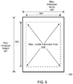
- FIG. 5 is a block diagram depicting an exemplary single interposer 500.
- Interposer 500 has a maximum interposer height 501 and a maximum interposer width 502. These maximum height 501 and width 502 are generally determined by lithography, and in particular may be limited by reticle imaging size. Additionally restricting maximum usable interposer area 510 are offsets 511 through 514 from edges of interposer 500. These offsets may be due to providing margins for packaging and assembly, such as a package lid, scribe lines, a seal ring, and under fill margining, as well as lithographic imaging.
- interposer 500 may be cut out of a silicon wafer by first using laser ablation to create trenches along scribe lines followed by cutting with a diamond tipped circular blade along such laser ablated trenches.
- Laser ablation may be used to reduce chipping or delamination along such edges in comparison with cutting with a diamond tipped circular blade alone.
- laser ablation tends to leave a wider trench than cutting with a diamond tipped circular blade.
- a maximum usable interposer height 503 and a maximum usable interposer width 504 may define a maximum usable interposer area 510. However, some of this area may be a restricted area. As described below in additional detail, for a left-side interposer of an interposer assembly, a right edge of a portion of area 510, such as offset region 512, for such left-side interposer may align with a left edge of an "interconnect restricted area.”
- interconnect restricted area it is generally meant a region associated with other regions which are not sufficiently reliable or otherwise not available for fine pitch alignment of operative fine pitch interconnects.
- a left edge of such right-side interposer may align with a right edge of such an interconnect restricted area.
- a top and bottom orientation may be used.
- An interconnect restricted area thus may include parts, such as offsets for example, of a first interposer and a second interposer, where signals are routed via a bridging die to avoid the interconnect restricted area of the first interposer and the second interposer.
- an offset region of an interposer may be at a far edge area of a reticle imaging field, imaging fine pitch interconnects at such far edge area may not be performed reliably.
- fine pitch interconnects may be reliably formed more towards the center of such reticle imaging field, for example such as used in the formation of a die bridging first and second interposers.
- fine pitch interconnects may not be reliably aligned in offset regions of first and second interposers, such fine pitch interconnects may be used to carry signals in a bridging die above such offset regions.
- fine pitch interconnects are formed outside of an interconnect restricted area of such first and second interposers, such that a plurality of components that interconnect the integrated circuit die to the first interposer and the second interposer are located outside the interconnect restricted area.
- conventional micro bumps for example may be located in an interconnect restricted area.
- an inter-reticle imaging field seam is where at least two image fields, whether from same or different reticles, of a lithographic operation overlap with one another.
- metal wires for one inter-die interposer interface such as for example from one group of micro bumps on one active die to another group of micro bumps on another active die, may be formed entirely within one interposer reticle field. More particularly, with respect to fine pitch interconnects, such inter-die interposer interface may be moved away from a far edge area of a reticle image field for an interposer.
- An interconnect restricted area in addition to being associated with areas of offsets, may optionally include a portion of otherwise usable area of interposer area 510, such as from a right-side and/or a left-side interposer for enhanced margin.
- an IC die such as an FPGA die bridges interposers which are joined together from a same wafer, for example bridges offset regions 511 and 512 from right and left interposers, respectively, of an interposer assembly, such as interposer assembly 310 or 410 for example.
- scribe line areas of such interposers below such FPGA die may form at least part of an interconnect restricted area.
- offsets may likewise be reduced as some edges of an interposer may not be cut or otherwise severed.
- scribe line area between such interposers may be reduced.
- scribe line areas on a wafer are generally uniform as between all dies thereof, even though in other embodiments scribe line areas on a wafer may not be generally uniform as between all dies thereof.
- offset areas may be at far edge areas of a lithographic imaging field, and as such it may not be possible to reliably form fine pitch interconnects in such offset areas.
- An interconnect restricted area is described at least with respect to being responsive to offset regions of interposers, and in some embodiments may include a gap between interposers and/or otherwise useable area of one or more interposers subject to lithographic imaging field geometric limitations.
- An interconnect restricted area may be defined as a design rule and/or layout rule for design of an interposer or interposers. In other words, such interconnect restricted area may be thought of as being on a die to which a bridging die is interconnected. Conductive lines as well as other interconnects of such interposers may likewise be associated with an interconnect restriction. Furthermore, a gap between interposers may likewise be associated with an interconnect restricted region.
- an interconnect restricted area is referred to herein as defined on interposers responsive at least to portions of offset regions of such interposers.
- an interconnect restriction region of an interposer is referred to herein as an offset region.
- an interconnect restricted area may be of any die, including an active die or a passive die, as an interposer may be an active device or a passive device. However, for purposes of clarity and not limitation, it shall be assumed that interposers are passive devices.
- a bridging die to connect one interposer to another interposer, whether severed or extended interposers, may be an active die or a passive die.
- fine pitch interconnects to a bridging die may be located on opposing sides of an interconnect restricted area of first and second interposers.
- maximum interposer height 501 may be approximately 31 mm (approximately 1.22 inches) after package lid footprint margining, and presently maximum interposer width 502 may be approximately 26 mm (approximately 1.024 inches) after package lid footprint margining.
- maximum usable interposer height 503 may be approximately 29 mm (approximately 1.142 inches), and maximum usable interposer width 504 may be approximately 24 mm (approximately 0.9449 inch).
- a maximum usable interposer area 510 may be approximately 700 mm 2 (approximately 27.56 square inches), and this maximum usable interposer area 510 should be considered in view of presently existing monolithic die sizes of approximately 600 mm 2 (approximately 23.62 square inches) or above for high-end devices.
- 1 gigabit of memory would have consumed approximately 25% to 50% of interposer usable area, and thus such an amount of memory could not be packaged with large high-end devices. This meant that pin counts density was significantly limited due to size of such interconnects.
- buffering using one gigabyte of memory may effectively only account for approximately 2.5 ms of 400 Gbps traffic, which may lead to an improper balance with respect to utilization of transceivers and line-system bridging.
- interposer area is provided by effectively bridging two or more interposers to provide a stacked die assembly.
- this may involve using one or more die interconnected to two or more interposers, where such interposer dies are formed on a same wafer as a single platform for providing a single IC package.
- the two or more interposers are physically connected to one another as a single platform, in contrast to an embodiment where two or more separated interposers make physical contact with each other.
- Reticle imaging fields used to form interposers may or may not overlap with one another.
- interposers are severed from one another.
- interposer dies may be completely severed from one another and then molded together for a single IC package, as described below for example, and bridged with a bridging die.
- FIG. 6-1 is a block diagram depicting an assembly according to the invention such as, e.g., stacked die assembly 600A.
- Stacked die assembly 600A includes SoC 300, memory pools 303A and 303B, and an interposer assembly of interposers 500A and 500B whether for an extended interposer or completely severed interposers 500A and 500B.
- SoC 300 is an FPGA; however, it should be understood that other types of ICs may be used.
- SoC 300 may include line-side transceivers 301, system-side transceivers 302A through 302C, and line-system bridge 304.
- Line-side transceivers 301 and system-side transceivers 302A through 302C may be coupled for bidirectional communication via line-system bridge 304, and such coupling may be an intra-die coupling, such as by using PIPs of an FPGA.
- Line-system bridge 304 may be implemented in FPGA programmable resources, namely "FPGA fabric".
- SoC 300 may be interconnected to both interposer 500A and 500B, such as to a surface of interposer 500A and to a surface of interposer 500B.
- SoC 300 may extend from an upper surface of interposer 500A to an upper surface of interposer 500B so as to bridge interposers 500A and 500B.
- interposers 500A and 500B are a common single platform formed of a same wafer.
- interposers 500A and 500B may be separated interposers coupled to one another via SoC 300.
- a portion of usable area 510 of interposer 500A bordering a left-most edge of offset region 515, as generally indicated by dotted line 710A, and/or a portion of usable area 510 of interposer 500B bordering a right-most edge of offset region 516, as generally indicated by dotted line 710B, may optionally be respective portions used to define an interconnect restricted area 599 in addition to being responsive to offset regions 515 and 516.
- interconnect restricted area 599 described below in additional detail is formed only responsive to offset regions 515 and 516, even though in other embodiments a portion of otherwise usable area 510 may be used.
- SoC 300 conventionally may have dense micro bumps or other fine pitch interconnects, including conductive line interconnect components, that fall within either or both of offset regions 515 and 516.
- the interconnect restricted area 599 of interposers includes interconnects, but it does not include fine pitch interconnects.
- offset regions 515 and 516 are not suitable for fine pitch interconnects, for SoC 300 to bridge interposers 500A and 500B, whether they are severed from one another or not, fine pitch "pinout" layout of such SoC 300 may not be conventional. Rather, fine pitch "pinout" layout of SoC 300 may be tailored to bridging interposers 500A and 500B.
- fine pitch interconnects of SoC 300 disposed over offset regions 515 and 516 may be aligned to coarse pitch interconnects that fall within offset regions 515 and 516, namely fall within interconnect restricted area 599, of interposers 500A and 500B.
- Memory pools 303A and 303B are interconnected to a surface of interposer 500B.
- memory pools 303A and 303B may be interconnected to an upper surface of interposer 500B for inter-die coupling with SoC 300.
- Memory pools 303A and 303B may be coupled to SoC 300 for bidirectional communication.
- Interposers 500A and 500B may have a same or a substantially same height. Width W1 of interposer 500A may be less than or equal to a maximum interposer width 502, and width W2 of interposer 500B likewise may be less than or equal to a maximum interposer width 502. However, width W1 may be substantially larger than width W2 in order to accommodate different die sizes.
- An interposer assembly of interposers 500A and 500B may have an overall interposer assembly width 602 of width W1 + W2.
- an overall interposer assembly width 602 of approximately 40 millimeters (approximately 1.575 inches) may be used with SoC 300 having a width of approximately 24 millimeters (approximately 0.9449 inch).
- stacked die assembly 600A may fit within a single 50 mm (1.969 inches) x 50 mm (1.969 inches) package.
- other heights, widths, and/or package sizes may be used.
- Interposer 500A and an edge of interposer 500B are positioned at least substantially side-by-side to one another. When interposers 500A and 500B are severed from one another, such edges of interposers 500A and 500B may abut one another.
- Interposer 500A has a reserved or offset region 515 proximal to interposer 500B. According to the invention, offset region 515 has a boundary that is coterminous with a far right edge of interposer 500A.
- Interposer 500B has a reserved or offset region 516 proximal to interposer 500A. According to the invention, offset region 516 has a boundary that is coterminous with a far left edge of interposer 500B.
- offset regions 515 and 516 may be accounted for in dense fine pitch pinout layout of SoC 300, where SoC 300 is formed to provide an electrical interconnection within restricted area 599 associated with offset regions 515 and 516 of interposers 500A and 500B, respectively, though not with fine pitch-to-fine pitch die-to-die interconnection.
- SoC 300 is formed to provide an electrical interconnection within restricted area 599 associated with offset regions 515 and 516 of interposers 500A and 500B, respectively, though not with fine pitch-to-fine pitch die-to-die interconnection.
- Either or both of offset regions 515 and 516 may be formed such that they include no metal layer portion and no via layer portion used to provide an operative fine pitch-to-fine pitch electrical interconnection, and thus SoC 300 may not include any pinouts for corresponding fine pitch interconnects associated within such offset regions 515 and 516.
- either or both of offset regions 515 and 516 may be formed such that they include no electrical interconnects and associated conductive lines.
- Electrical interconnects are used to carry signal for operation of a device. Electrical interconnects may be contrasted from non-electrical interconnects for nonelectrical structures, such as for example dummy structures, such as may be used for example for lithographic imaging or otherwise.
- Fine pitch die-to-die interconnects such as die-to-die interconnects described below for example, for interconnecting SoC 300 to memory pools 303A and 303B via interposer 500B may be exclusively located on interposer 500B outside of offset region 516. All fine pitch conductive lines for interconnecting SoC 300 to memory pools 303A and 303B may be formed as part of interposer 500B outside of offset region 516.
- interconnect restricted area 599 is free of any operative interconnects, even though in other embodiments interconnects not subject to fine pitch alignment restrictions may be present in such interconnect restricted area 599.
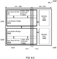
- FIG. 6-2 is a block diagram depicting another exemplary stacked die assembly 600B.
- Stacked die assembly 600B is generally the same as stacked die assembly 600A of FIG. 6-1 , except for the following differences.
- stacked die assembly 600B includes two SoCs, namely SoC 300A and SoC 300B.
- SoC 300A includes line-side transceivers 301, system-side transceivers 302A and line-system bridge 304A
- SoC 300B includes system-side transceivers 302B and 302C and line-system bridge 304B.
- SoCs 300A and 300B may be interconnected to one another via interconnects associated with interposer 500A.
- FIG. 6-3 is a block diagram depicting yet another example of a stacked die assembly 600C.
- Stacked die assembly 600C is generally the same as stacked die assembly 600B of FIG. 6-2 , except for the following differences.
- SoC 300A includes line-side transceivers 301A and system-side transceivers 302A, as well as line-system bridge 304A
- SoC 300B includes line-side transceivers 301B and system-side transceivers 302B, as well as line-system bridge 304B.
- Each of SoCs 300A and 300B may bridge offset regions 515 and 516 for coupling interposers 500A and 500B to one another or for interposers 500A and 500B not severed from one another.
- Approximately equal amounts of semiconductor area may be provided for forming line-side and system-side transceivers, and two SoCs may be used to physically bridge interposers 500A and 500B.
- transceiver resources may be configured either for line-side or system-side.
- interposers such as interposers 500A and 500B
- a mask set used to form interposer 500A may be substantially different from a mask set used to form interposer 500B.
- an SoC die may be substantially different than a memory die, including without limitation substantially different sizes and pinouts.
- interposer assembly By providing an interposer assembly as described herein, it should be understood that more transceivers, as well as more resources generally, for line-system bridging may be implemented in a single IC package along with buffer memory. Furthermore, the amount of memory may be substantially increased owing to having a larger interposer assembly footprint. Because such resources may be collectively mounted to an interposer assembly for an IC package, die-to-die interconnects may be formed with dense micro bumps for example which are significantly smaller than conventional micro bumps and substantially smaller than micro-balls. Micro-balls, which are sometimes referred to C4 solder balls, are significantly larger than conventional micro bumps and are conventionally used for an IC -to-IC interconnect via a PCB.
- interconnect density is enhanced by providing an interposer assembly with a larger footprint within a package, because more area is provided for fine pitch die-to-die interconnection, which may be used instead of conventional die-to-die interconnects and/or chip-to-chip interconnects.
- bandwidth may correspondingly be increased by virtue of such interconnect density.
- Bandwidth increase may be further aided by an additional amount of resources available within a packaged stacked die assembly having a large interposer assembly for supporting such additional resources.
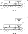
- FIG. 7-1 is a block diagram depicting an exemplary cross-sectional view of any of stacked die assemblies 600A, 600B, and 600C (collectively and singly "stacked die assembly 600") of FIGS. 6-1 , 6-2 , or 6-3 , respectively.
- SoC 300 and memory pool 303 are interconnected to an interposer assembly formed of interposers 500A and 500B via interconnects 713.
- Interconnects 713 in this example are dense die-to-die flip-chip micro bumps; however, other types of die-to-die fine pitch interconnects may be used.
- SoC 300 is connected to upper surface 703 of interposer 500A via a portion of die-to-die interconnects 713, which may be fine pitch interconnects or may be conventional flip-chip micro bumps, and is connected to upper surface 704 of interposer 500B via another portion of die-to-die interconnects 713.
- Memory pool 303 is connected to upper surface 704 of interposer 500B via yet another portion of die-to-die interconnects 713.
- Some of die-to-die interconnects 713 may be coupled to other larger interconnects, which are referred to herein as "connectors" 711 so as not to be confused with die-to-die interconnects ('interconnects”) 713.
- connectors 711 are coupled to interconnects 713 using "through-substrate vias", such as through-silicon vias (“TSVs”) 712 for example.
- TSVs through-silicon vias
- connectors 711 are micro-balls; however, other types of chip-to-chip large-scale interconnects may be used.
- connectors 711 are substantially larger than interconnects 713. Accordingly, by providing an interposer assembly formed of interposers 500A and 500B, which may be joined to or severed from one another, a larger interposer area for interconnecting dies is provided so as to avoid having to use chip-to-chip interconnects. According to the invention, interposers 500A and 500B are severed from one another, namely separate dies.
- interposers 500A and 500B are silicon interposers, and thus for this example, through-substrate vias are TSVs 712; however, in other embodiments other types of substrates or die platforms may be used.
- a far right edge 701 of interposer 500A according to the invention abuts a far left edge 702 of interposer 500B.
- Edges 701 and 702 respectively provide boundaries of offset regions 515 and 516, as previously described herein.
- offset regions 515 and 516 of interposers 500A and 500B, respectively are free of active fine pitch interconnects and associated conductive lines, namely an interconnect restricted area or region 710 which may correspond to all or portions of offset regions 515 and 516.
- interconnects 713 on upper surface 704 of interposer 500B are for interconnecting SoC 300 and memory pool 303.
- Conductive lines such as conductive line 715 (hereinafter singly and collectively "conductive lines 715"), which may for example be between layers of interposer 500B, are used to couple a portion of interconnects 713 located between SoC 300 and upper surface 704 with another portion of interconnects 713 located between memory pool 303 and upper surface 704.
- all conductive lines 715 for interconnecting SoC 300 and memory pool 303 may be provided as part of interposer 500B.
- all conductive lines 715 for die-to-die interconnection may be self-contained within interposer 500B.
- Interconnects 713 and conductive lines 715 are examples of components that may be used to interconnect SoC 300 to memory pool 303. Interconnects 713 and conductive lines 715 may singly and collectively provide fine pitch interconnects.
- FIG. 7-2 is a block diagram depicting a cross-sectional view of another exemplary stacked die assembly 700.
- Stacked die assembly 700 is similar to stacked die assembly 600, except memory pool 303 is replaced with a vertical stack of memory dies interconnected to one another, namely stacked die memory 720.
- Stacked die memory 720 may include memory pool dies ("memory pools") 303-1 through 303-N, for N a positive integer greater than one. Even though not shown for purposes of clarity and not limitation, it should be understood that memory pool dies 303-1 through 303-N may be interconnected to one another, such as through use of TSVs for example, to provide stacked die memory 720.
- Memory pool die 303-1 may be interconnected to interposer 500B as previously described for example with reference to memory pool 303.
- FIG. 7-3 is a block diagram depicting a cross-sectional view of yet another stacked die assembly 700.
- memory pool dies 303-1 through 303-N are stacked on top of a memory interface 731 for forming a stacked die memory 730.
- Stacked die memory 730 replaces stacked die memory 720.
- Memory interface 731 is interconnected to interposer 500B.
- Memory interface 731 may include interface logic for memory pool dies 303-1 through 303-N.
- Memory interface 731 is interconnected to a memory pool die 303-1 and may be interconnected to each of memory pool dies 303-1 through 303-N through one or more intervening memory pool dies thereof depending on configuration of stacked die memory 730.
- FIG. 8 is a block diagram depicting an exemplary top view of an interposer assembly 800.
- Interposer assembly 800 includes interposers 500A and 500B.
- Each of interposers 500A and 500B has a height which may be equal to or less than a maximum interposer height 501.
- both of interposers 500A and 500B in this example have a same maximum interposer height 501 and likewise have a same maximum usable height 503.
- interposers 500A and 500B may have unequal heights at least one of which is not at a maximum height.
- Each of interposers 500A and 500B has a width which may be equal to or less than a maximum interposer width 502.
- a maximum interposer width 502. For purposes of clarity by way of example and not limitation, both of interposers 500A and 500B in this example have a same maximum interposer width 502 and likewise have a same maximum usable width 504. However, in other embodiments, interposers 500A and 500B may have unequal widths at least one of which is not a maximum width.
- electrical interconnect restricted area 710 is not defined responsive to abutting diced edges of interposers 500A and 500B, as interposers 500A and 500B in this example are formed on a same wafer or other substrate as a whole, namely are formed integral to one another as a single platform.
- interposers 500A and 500B are formed as a single platform in contrast to two separate platforms.
- interposers 500A and 500B in this example are from a same semiconductor substrate to provide a single platform. Offset regions 515 and 516 of interposers 500A and 500B may be used to define an electrical interconnect restricted area 710.
- interposers 500A and 500B when interposers 500A and 500B are formed as a single platform, electrical interconnect restricted area 710 need not include a scribe line seam and need not include margining for dicing for packaging. Thus, in an extended or single platform version of interposers 500A and 500B, maximum usable area may be increased over an embodiment where interposers 500A and 500B are diced to provide separate dies thereof, and accordingly, footprint of interconnect restricted area 710 may be reduced subject to interposer reticle field lithographic imaging limitations.
- Interconnect restricted area 710 may be enlarged to mitigate against alignment issues.
- substrates including without limitation glass or another form of substrate base material.
- FIG. 9-1 is a block diagram depicting an exemplary wafer 900.
- Wafer 900 may be used for forming interposer assemblies 800 of interposers 500A and 500B. Two separate reticle sets may be used to print interposer patterns, including without limitation wires and vias, for forming interposers 500A and 500B.
- Wafer 900 may be laser ablated and/or sawn along horizontal rows 901 and vertical columns 902. Horizontal rows 901 and vertical columns 902 may be scribe lines. It should be appreciated that after dicing wafer 900, interposer assemblies 800, having interposers 500A and 500B formed integral to one another of the same wafer substrate material, are provided as dies of a single platform.
- FIG. 9-2 is a block diagram depicting an exemplary wafer 900 with interposer assemblies 800 formed of four interposers each.
- interposer assemblies 800 each include interposers 500A, 500B, 500C, and 500D, where such collection of interposers are formed integral to one another as single or common platform.
- FIG. 10-1 is a block diagram depicting a cross-sectional view of an exemplary stacked die assembly 1000, not forming part of the invention.
- Stacked die assembly 1000 is similar to stacked die assembly 600, except that rather than abutting edges 701 and 702, a gap 1010 between such edges is provided. Edges 701 and 702 may or may not be position at lease substantially parallel to one another for such side-by-side orientation.
- gap 1010 effectively extends a restricted interconnect area 1049, and accordingly, as what might otherwise be pinouts under SoC 300 extending above gap 1010 may be omitted.
- a die other than SoC 300 may be used to bridge interposers 500A and 500B.
- interposers 500A and 500B have a gap 1010 between them, then a seam associated with reticle fields used to form such interposers may not exist if such interposers are formed from different wafers.
- offset regions 515 and 516 persist, and thus for purposes of clarity and not limitation it shall be assumed that an interconnect restricted region or area 1049 persists and includes gap 1010.
- FIG. 10-2 is a block diagram depicting a cross-sectional view of an exemplary stacked die assembly 1100, not forming part of the invention.
- Stacked die assembly 1100 is similar to stacked die assembly 1000, except for the following differences.
- SoC 300C does not bridge interposers 500A and 500B, and thus SoC 300C is interconnected only to interposer 500A in this example.
- a bridge die 1110 is added to interconnect an upper surface of interposer 500A and to an upper surface of interposer 500B.
- Bridge die 1110 spans offset regions 515 and 516, as well as gap 1010 between interposers 500A and 500B, for physically bridging such interposers.
- each of interposers 500A and 500B optionally may be used to provide interconnect restricted area or region 710, as previously described.
- image quality generally along edges of image fields associated with one or more reticles used in manufacturing interposer 500A and 500B may be sufficiently degraded so as to make reliably forming fine pitch interconnects in areas or regions associated with such edges problematic.
- fine pitch interconnects 713 and fine pitch conductive lines 715 respectively associated with interposer 500A and 500B are all outside of offset regions 515 and 516.
- bridge die 1110 may be a passive device.
- bridge die 1110 may itself be a silicon interposer. However, whether a passive or an active die, bridge die 1110 may be manufactured to have a pinout that accounts for offset regions 515 and 516, as well as gap 1010.
- bridge die 1110 may be interconnected to SoC 300C via interposer 500A using associated fine pitch micro bumps. Moreover, bridge die 1110 may be interconnected to a memory pool die 303 via interposer 500B using associated fine pitch micro bumps.
- Bridge die 1110 may optionally be an active die.
- bridge die 1110 may provide a bidirectional communication bridge between SoC 300C and memory pool 303.
- bridge die 1110 may include buffers and/or pipelined flip-flops for die-to-die communication.
- bridge die 1110 may provide an interconnection network between SoC 300C and memory pool 303, such as for switching for example.
- Bridge die 1110 may optionally include an array of bidirectional repeaters 1111 or a set of crossbar switches 1111, where each such bidirectional repeater or crossbar switch 1111 may be statically configured to be either transferring signals from a first IC to a second IC, such as for example from SoC 300C to memory pool 303, and/or the other way round.
- configuration bits for such array of bidirectional repeaters 1111 may eventually be stored inside bridge die 1110, although such configuration bits may be initialized by one of such other ICs, such as SoC 300C or memory pool 303 for example.
- such crossbar switches 1111 may be statically configured.
- a P-by-Q-by-W (“PxQxW”) crossbar switch 1111 has P input ports, Q output ports, and W bits per port, and may be implemented as Q instances of a P-to-1 mux with a W-bit-wide datapath.
- Select control lines of these P-to-1 muxes can be static so traffic between the first and the second ICs, such as between SoC 300C and memory pool 303 for example, does not have to go straight.
- Two crossbar switches 1111 may be used to allow traffic to be able to go from a first IC to a second IC and/or the other way round.
- offset region 515 provides a first portion of an electrical interconnect restricted area of interposer 500A outside of which fine pitch interconnects, as well as fine pitch conductive lines associated therewith, for interconnecting bridge die 1110 to interposer 500A for interconnection to SoC 300C may be formed.
- offset region 516 provides a second portion of an electrical interconnect restricted area of interposer 500B outside of which fine pitch interconnects, as well as fine pitch conductive lines associated therewith, for interconnecting bridge die 1110 to interposer 500B for interconnection to memory pool 303 may be formed.
- fine pitch interconnects of bridge die 1110 for bidirectional repeaters 1111 or crossbar switches 1111 may be outside of and/or extend above interconnect restricted area 1049 though are generally not available for gap 1010.
- FIG. 11 is a flow diagram depicting an exemplary process 1150, not forming part of the invention, for forming one or more of stacked die assemblies 1100.
- Stacked die assemblies 1100 are similar to stacked die assembly 1100 of FIG. 10-2 , except for the following differences. Furthermore, even though an example of stacked die assembly 1100 is used, it should be understood that stacked die assembly 1000 may be used in such process 1150.
- interposers 500A and 500B are formed as separate die for forming pairs thereof. Accordingly, interposers 500A and 500B may be diced from same or separate wafers. By way of example not limitation, one wafer may be used exclusively for forming interposers 500A, and another wafer may be used exclusively for forming interposers 500B.
- interposers 500A and 500B formed at 1101 are placed into or otherwise put in contact with a molding or packaging material 1120. Effectively at 1102, a wafer or other substrate may be re-constructed with interposers 500A and 500B in respective pairs using a mold. It should be appreciated that a portion of such packaging material 1120 extends between pairs of interposers 500A and 500B, namely extends into gap 1010.
- SoC 300C, bridge die 1110, and memory pool 303 may be interconnected to interposers 500A and 500B, as previously described herein.
- stacked die assemblies 1100 may be diced from such molded substrate.
- unitary stacked die assemblies 1100 may be provided as set in packaging material 1120, where each such unitary stacked die assembly 1100 has a portion of packaging material 1120 extending between an edge of interposer 500A and an edge of interposer 500B.
- Having two or more separate interposers with one or more bridge die may reduce stress. Furthermore, separate interposers may allow for combinations thereof to be customized by changing one or more of such interposer to accommodate different types of ICs. Total yield may be improved with a combination of separate interposers, as known good interposers may be combined to form interposer assemblies. Separate interposers may reduce warping, which may increase assembly yield during top die assembly on interposers. Separate interposers may reduce underfilling of fine pitch interconnects.
- the large size of a single interposer may induce large amounts of stress on the interposer and on other IC structures that couple to the interposer.
- solder bumps below the interposer that couple the interposer to the substrate of an IC package can be exposed to a significant amount of stress that is dependent upon the size of the interposer.
- the interposer can be split or subdivided into two or more individual interposers rather than using a single, monolithic interposer.
- the smaller interposers and any IC structure coupled to the smaller interposers are subjected to reduced stress, thereby increasing reliability of the multi-die IC structure.
- FIG. 12 is a block diagram illustrating a topographic view of an IC structure 1200, not forming part of the invention.
- IC structure 1200 is a multi-die IC structure.
- FIG. 12 illustrates a packing approach to stacking multiple dies of IC structure 1200 within a single package.
- IC structure 1200 can include a plurality of dies 1205, 1210, and 1215. Dies 1205-1215 can be mounted on two or more interposers 1220 and 1225. Interposers 1220 and 1225 each can be implemented as a silicon interposer. Interposers 1220 and 1225 can be mounted on a substrate 1230 of an IC package within which IC structure 1200 can be implemented.
- Each of interposers 1220 and 1225 can be a die having a planar surface on which dies 1205-1215 can be horizontally stacked. As shown, dies 1205 and 1210 can be located on the planar surfaces of interposers 1220 and 1225 side-by-side. In the example shown in FIG. 12 , die 1205 is mounted only to interposer 1220. Die 1215 is mounted only to interposer 1225. Die 1210 is mounted to both interposer 1220 and to interposer 1225. In general, each of dies 1205-1215 can be coplanar. Similarly, each of interposers 1220 and 1225 can be coplanar. As used within this specification, the term "coplanar" means that the enumerated structures are located in a same plane or that each enumerated structure has at least one surface that is in a same plane as the others.
- Each of interposers 1220 and 1225 can provide a common mounting surface and electrical coupling point for one or more dies of a multi-die IC structure. Interposers 1220 and 1225 can serve as an intermediate layer for interconnect routing between dies 1205-1215 or as a ground or power plane for IC structure 1200. Each of interposers 1220 and 1225 can be implemented with a silicon wafer substrate, whether doped or un-doped with an N-type and/or a P-type impurity. The manufacturing of interposers 1220 and 1225 can include one or more additional process steps that allow the deposition of one or more layer(s) of metal interconnect. These metal interconnect layers can include aluminum, gold, copper, nickel, various silicides, and/or the like.
- Interposers 1220 and 1225 can be manufactured using one or more additional process steps that allow the deposition of one or more dielectric or insulating layer(s) such as, for example, silicon dioxide.
- interposer 1220 and/or 1225 can be implemented as passive dies in that one or both of interposers 1220 and/or 1225 can include no active circuit elements, e.g., no P-material in contact with N-material or "PN" junctions.
- interposers 1220 and 1225 can be manufactured using one or more additional process steps that allow the creation of active circuit elements such as, for example, transistor devices and/or diode devices.
- each of interposers 1220 and 1225 is, in general, a die and is characterized by the presence of one or more TSVs as will be described in greater detail within this specification.
- FIG. 13-1 is a block diagram illustrating a cross-sectional side view of IC structure 1200 of FIG. 12 , not forming part of the invention. More particularly, FIG. 13-1 illustrates a view of IC structure 1200 of FIG. 12 taken along cut-line 13-1-13-1. As such, like numbers will be used to refer to the same items throughout this specification.
- a first (bottom) surface of interposer 1220 can be coupled to a top surface of substrate 1230.
- a first (bottom) surface of interposer 1225 can be coupled to the top surface of substrate 1230.
- a second (top) surface of interposer 1220 can be coupled to a bottom surface of die 1205 and to a portion of a bottom surface of die 1210.
- a second (top) surface of interposer 1225 can be coupled to a portion of the bottom surface of die 1210 and to a bottom surface of die 1215.
- dies 1205-1215 can be electrically coupled to interposers 1220 and 1225 via solder bumps 1305.
- Solder bumps 1305 can be implemented in the form of "micro-bumps," for example. More particularly, die 1205 is coupled to interposer 1220 through solder bumps 1305. Die 1210 is coupled to interposer 1220 and to interposer 1225 through solder bumps 1305. Die 1215 is coupled to interposer 1225 through solder bumps 1305. Each of solder bumps 1305 also can serve to physically attach dies 1205-1215 to interposer 1220 and/or to interposer 1225 as the case may be.
- Interposer 1220 can include one or more patterned layers formed of metal or another conductive material forming interconnect region 1310. The patterned layers can be used to form inter-die wires such as inter-die wire 1315 that can pass inter-die signals between dies 1205 and 1210.
- inter-die wire 1315 can be formed using one or more of the patterned metal layers in combination with one or more vias from interconnect region 1310.
- Inter-die wire 1315 can connect to one of solder bumps 1305 located between die 1205 and interposer 1220 and to another one of solder bumps 1305 located between die 1210 and interposer 1220, thereby coupling die 1205 to die 1210 and allowing the exchange of signals between dies 1205 and 1210.
- Interposer 1225 can include one or more patterned layers formed of metal or another conductive material forming interconnect region 1320.
- Interconnect region 1320 can be substantially similar to interconnect region 1310 of interposer 1220. Accordingly, the patterned layers and vias can be used to form inter-die wires such as inter-die wire 1325.
- Inter-die wire 1325 can connect to one of solder bumps 1305 located between die 1210 and interposer 1225 and to another one of solder bumps 1305 located between die 1215 and interposer 1225, thereby coupling die 1210 to die 1215 and allowing the exchange of signals between dies 1210 and 1215.
- solder bumps 1305 a variety of other techniques can be used to couple dies 1205-1215 to interposers 1220 and 1225.
- bond wires or edge wires can be used to couple a die to one or more interposers.
- an adhesive material can be used to physically attach a die to one or more interposers.
- the coupling of dies 1205-1215 to interposers 1220 and 1225 via solder bumps 1305, as illustrated within FIG. 13-1 is provided for purposes of illustration and is not intended to limit the examples disclosed within this specification.
- Solder bumps 1330 can be used to electrically couple the bottom surface of each of interposers 1220 and 1225 to substrate 1230.
- solder bumps 1330 can be implemented in the form of "C4-bumps.”
- substrate 1230 can be part of a multi-die IC package in which IC structure 1200 is implemented.
- Solder bumps 1330 can be used to couple IC structure 1200 to a node external to the multi-die IC package.
- each of interposers 1220 and 1225 can include one or more through-silicon vias (TSVs) 1335.
- each TSV 1335 can be implemented as a via formed of conductive material to form an electrical connection that vertically transverses, e.g., extends through a substantial portion, if not the entirety of, interposer 1220 and/or interposer 1225.
- TSVs 1335 can be implemented by drilling or etching an opening into interposer 1220 and/or interposer 1225 that extends from a top planar surface, i.e., the surface to which solder bumps 1305 are coupled, through to a bottom planar surface, i.e., the surface to which solder bumps 1330 are coupled.
- Conductive material then can be deposited within the openings. Examples of conductive material that can be used to fill the openings to form TSVs 1335 can include, but are not limited to, aluminum, gold, copper, nickel, various silicides, and/or the like.
- each TSV 1335 is shown to couple to solder bumps 1305 through one or more of the patterned layers in combination with one or more vias within interconnect region 1310 in interposer 1220 or within interconnect region 1320 in interposer 1225.
- TSVs 1335 can extend substantially through interposer 1220 and interposer 1225 to couple solder bumps 1305 with solder bumps 1330 by passing through interconnect region 1310 or interconnect region 1320 as the case may be.
- TSVs 1335 in combination with solder bumps 1305 and solder bumps 1330, couple die 1205 to substrate 1230 via interposer 1220.
- Die 1210 is coupled to substrate 1230 using TSVs 1335, solder bumps 1305, and solder bumps 1330 through interposer 1220 and through interposer 1225.
- Die 1215 is coupled to substrate 1230 using TSVs 1335, solder bumps 1305, and solder bumps 1330, through interposer 1225.
- signals can be propagated from die 1205 to die 1215 through inter-die wires such as inter-die wire 1315 and inter-die wire 1325 in combination with wires or other signal paths implemented within die 1210 that couple inter-die wire 1315 with inter-die wire 1325.
- the signal paths implemented within die 1210 can be implemented in the form of hardwired circuitry or programmable circuitry.
- dies 1205-1215 can be implemented as any of a variety of different types of dies.
- One or more of dies 1205-1215 can be implemented as a memory device, a processor, e.g., a central processing unit, an application-specific IC, or a programmable IC.
- Each such type of IC can include hardwired circuitry coupling inter-die wire 1315 with inter-die wire 1325.
- Each of dies 1205-1215 can be implemented as a similar or same type of IC.
- die 1205 can be implemented as first type of IC, while dies 1210 and 1215 are implemented as a second and different type of IC.
- each of dies 1205-1215 can be implemented as a different type of IC.
- the signal paths in die 1210 that couple inter-die wire 1315 to inter-die wire 1325 can be hardwired or programmable circuitry.
- die 1205 can be rendered unable to communicate with die 1215 unless or until programmable circuitry is configured to implement such a connection.
- interposer 1220 and interposer 1225 can be separated by a distance 1340.
- the respective edge of each of interposers 1220 and 1225 effectively forms a channel having a width equal to distance 1340 that extends between each of interposers 1220 and 1225.
- die 1210 effectively spans the channel between interposer 1220 and interposer 1225.
- Each of interposers 1220 and 1225 can have a length of L int .
- Substrate 1230 can have a length of L sub . Though illustrated as having a same length, each of interposers 1220 and 1225 can have different lengths depending upon the implementation of IC structure 100.
- IC structure 1200 is subjected to a variety of different stresses.
- interposers 1220 and 1225 are subjected to stress as each provides a structural base upon which dies are mounted.
- Further solder bumps and, in particular, solder bumps 1330 can be subjected to increased levels of stress.
- solder bumps 1330 that are located along one or more or all edges edge of interposer 1220 and/or 1225 can be subjected to increased levels of shear strain.
- solder bumps 1330 that are subjected to increased levels of shear strain are illustrated with shading as opposed to the solid coloration of the other ones of solder bumps 1330.
- the left-most and right-most solder bumps 1330 beneath interposer 1220 are subjected to a higher level of shear strain than other ones of the solder bumps 1330 between interposer 1220 and substrate 1230.
- the left-most and right-most of solder bumps 1330 beneath interposer 1225 are subjected to a higher level of shear strain than other ones of solder bumps 1330 between interposer 1225 and substrate 1230.
- shear strain (y) can be determined according to equation (1) below.
- ⁇ ⁇ thermal l ⁇ ⁇ h
- ⁇ thermal represents the thermal expansion coefficient
- l represents length
- ⁇ ⁇ represents the difference in the angle ⁇ before application of shear strain and after application of shear strain as shown in FIG. 13-2
- h represents height.
- the angle ⁇ is initially zero when solder bump 1330A is not exposed to shear strain. After solder bump 1330A is located between interposer 1225 and substrate 1230, thereby exposing solder bump 1330A to shear strain, solder bump 1330A flattens.
- the vertex of ⁇ is the center of the bottom flattened portion of solder bump 1330A.
- the angle ⁇ is measured as shown from the center line aligned with the vertex to the end point of the top flattened portion of solder bump 1330A in contact with interposer 1225, e.g., approximately one half of the top flattened portion of solder bump 1330A in contact with interposer 1225.
- Equation (1) can be applied to FIG. 13-1 to determine the shear strain to which solder bump 1330A, for example, is subjected.
- the variable l represents a length measured from a center of an interposer, i.e., interposer 1225 in this case, to an outer edge solder bump 1330A. In this example, l is one-half of L int .
- the variable h represents the height of solder bump 1330A.
- the coefficient of thermal expansion is, in effect, the difference between the coefficient of thermal expansion for substrate 1230 and the coefficient of thermal expansion for interposer 1225. For purposes of discussion, it can be assumed that the coefficient of thermal expansion for interposer 1225 is approximately 3 and the coefficient of thermal expansion for substrate 1230 is approximately 12. Accordingly, equation (1) can be reduced to equation (2) below.
- ⁇ 9 l ⁇ ⁇ h
- the shear strain is generally dependent upon the length of each interposer, e.g., L int .
- the shear strain to which solder bump 1330A is subjected can be reduced by reducing L int , which also reduces l . Accordingly, rather than using a single, monolithic interposer, shear strain on solder bump 1330A and on other bumps similarly positioned, can be reduced by using two or more smaller interposers, e.g., interposers that have reduced length compared to a single, monolithic interposer.
- FIG. 14 is a block diagram illustrating a topographic view of an IC structure 1400, not forming part of the invention.
- IC structure 1400 is a multi-die IC structure.
- IC structure 1400 can include a plurality of dies 1405, 1410, and 1415.
- Dies 1405-1415 can be coplanar and, as such can be mounted on interposers 1420, 1425, 1430, and 1435.
- Each of interposers 1420-1435 can be implemented as a silicon interposer substantially as described with reference to FIGs. 12 and 13 .
- Interposers 1420-1435 can be coplanar and mounted on a substrate of an IC package within which IC structure 1400 can be implemented. For ease of illustration, the substrate is not shown in FIG. 14 .
- IC structure 1400 is shown superimposed over a Cartesian coordinate system in which the X-axis bisects IC 1400 into two equal halves and the Y-axis bisects IC structure 1400 into two equal halves.
- the X-axis is perpendicular to the Y-axis.
- interposer 1420 is located entirely within quadrant 1.
- Interposer 1425 is located entirely within quadrant 2.
- Interposer 1430 is located entirely within quadrant 3.
- Interposer 1435 is located entirely within quadrant 4.
- each interposer 1420-1435 can be referred to as the first surface.
- the top surface of each interposer 1420-1435 to which the dies are mounted can be referred to as the second surface.
- die 1405 is mounted on a portion of the second surface of interposer 1420 and a portion of the second surface of interposer 1425. Die 1405 is located within only quadrants 1 and 2.
- Die 1410 is mounted on a portion of the second surface of each of interposers 1420-1435 and is partly within each of quadrants 1-4.
- Die 1415 is mounted on a portion of the second surface of interposer 1430 and a portion of the second surface of interposer 1435. Thus, die 1415 is located only within quadrants 3 and 4.
- Each of interposers 1420 and 1425 can include one or more inter-die wires that can be used to couple die 1405 with die 1410.
- each of interposers 1430 and 1435 can include one or more inter-die wires that can be used to couple dies 1410-1415.
- Die 1410 can be configured with wires or signal paths that can couple interposer 1420 to one, or more or each of interposers 1425, 1430, and 1435.
- die 1410 can be configured with wires or signals that can couple interposer 1425 with one, or more or each of interposers 1420, 1430, and 1435.
- Die 1405 can be configured with wires or signal paths that can couple interposer 1420 to interposer 1425.
- die 1415 can be configured with wires or signal paths that can couple interposer 1430 with interposer 1435.
- each of interposers 1420-1435 can include one or more TSVs.
- die 1405 can be coupled to the substrate through one or more TSVs located within interposer 1420 and/or one or more TSVs located within interposer 1425.
- Die 1410 can be coupled to the substrate through one or more TSVs located within interposer 1420, interposer 1425, interposer 1430, and/or interposer 1435.
- Die 1415 can be coupled to the substrate through one or more TSVs located within interposer 1430 and/or one or more TSVs located within interposer 1435.
- interposer 1420 can be separated from interposer 1435 by a predetermined distance 1440.
- interposer 1425 can be separated from interposer 1430 by the predetermined distance 1440. Accordingly, the separation described effectively forms a channel along the X-axis having a width of the distance 1440. Die 1410 effectively spans distance 1440 of the channel formed on the X-axis shown.
- Interposer 1420 can be separated from interposer 1425 by a predetermined distance 1445.
- interposer 1430 can be separated from interposer 1435 by the predetermined distance 1445. Accordingly, the separation described effectively forms a channel along the Y-axis having a width of the distance 1445.
- Each of dies 1405, 1410, and 1415 effectively spans distance 1445 of the channel formed on the Y-axis shown.
- FIG. 15 is a block diagram illustrating a cross-sectional side view of IC structure 1400 of FIG. 14 . More particularly, FIG. 15 illustrates a view of IC structure 1400 of FIG. 14 taken along cut-line 15-15. FIG. 15 illustrates the reduced length l that is achieved by using two or more interposers as opposed to a single, larger or monolithic interposer. Referring to FIG. 15 , the particular ones of solder bumps 1505 that are subjected to increased levels of shear strain are illustrated with shading as opposed to the solid coloration of other ones of solder bumps 1505. In this example, four interposers are used, thereby reducing l and reducing the amount of shear strain placed on solder bumps 1505A-1505D.
- Interposer 1430 can include an interconnect region 1510 that can be implemented as described with reference other interconnect regions already described within this specification.
- One or more inter-die wires formed within interconnect region 1510 can couple die 1410 and die 1415.
- interposer 1435 can include an interconnect region 1515 that can be implemented as previously described.
- One or more inter-die wires formed within interconnect region 1515 can couple die 1410 to die 1415.
- FIG. 15 also illustrates that interposer 1430 and interposer 1435 each can include one or more TSVs 1520. TSVs 1520 allow dies to couple to a substrate through an interposer to connect to nodes external to IC structure 1400 and external to the IC package.
- FIG. 16 is a block diagram illustrating a further cross-sectional side view of IC structure 1400 of FIG. 14 . More particularly, FIG. 16 illustrates a view of IC structure 1400 of FIG. 14 taken along cut-line 16-16.
- interposer 1435 can include one or more inter-die wires such as inter-die wire 1530 coupling die 1415 with die 1410.
- interposer 1420 can include an interconnect region 1525 that can be used to form one or more inter-die wires such as inter-die wire 1535.
- Inter-die wire 1535 can couple die 1410 with die 1405.
- FIG. 17 is a block diagram illustrating a topographic view of an IC structure 1700, not forming part of the invention.
- IC structure 1700 is a multi-die IC structure. As pictured, IC structure 1700 can include a plurality of dies 1705 and 1710. Dies 1705-1710 can be coplanar and mounted on interposers 1715 and 1720. Interposers 1715 and 1720 each can be implemented as a silicon interposer substantially as described within this specification. Interposers 1715 and 1720 can be coplanar and mounted on a substrate of an IC package within which IC structure 1700 can be implemented. For ease of illustration, the substrate is not illustrated in FIG. 17 .
- a first (bottom) surface of interposer 1715 can be coupled to a top surface of the substrate, e.g., using solder bumps such as C4 type solder bumps.
- a first (bottom) surface of interposer 1720 can be coupled to the top surface of the substrate also using solder bumps such as C4 type bumps.
- a second (top) surface of interposer 1715 can be coupled to a portion of a bottom surface of die 1705 and to a portion of a bottom surface of die 1710.
- a second (top) surface of interposer 1720 can be coupled to a portion of a bottom surface of die 1705 and to a portion of a bottom surface of die 1710.
- Dies 1705 and 1710 can be coupled to interposers 1715 and 1720 through solder bumps such as micro-bumps as previously described.
- Each of interposers 1715 and 1720 can include one or more TSVs through which dies 1705 and 1710 can couple to the substrate. As such, die 1705 can couple to the substrate through both interposer 1715 and interposer 1720. Similarly, die 1710 can couple to the substrate through both interposer 1715 and interposer 1720. Each of interposers 1715 and 1720 can include an interconnect region having one or more inter-die wires that support the exchange of signals between dies 1705 and 1710.
- multiple dies may be interconnected to one another over a larger interposer area than previously available by using multiple interposers.
- memory such as DRAM
- SSIT-based FPGA die stack Even though the example of adding memory, such as DRAM, to an SSIT-based FPGA die stack was used, it should be understood that the following description applies to any stacked die assembly in which die-to-die interconnects are enhanced by use of multiple interposers within a same package.
- a stacked die assembly as described herein may not be as constrained by current lithography, margining for packaging and assembly, and/or availability of die-to-die interconnects.
- the interposers in the multiple-interposer examples described herein may be active interposers, namely interposers with active components.
Claims (12)
- Ensemble de puces empilées pour des puces de circuit intégré d'un dispositif à circuit intégré, comprenant :un premier interposeur (500A) formé sur une tranche, le premier interposeur ayant une première région de décalage (515) qui fait partie d'une zone d'interconnexion restreinte (710), la première région de décalage (515) ayant une première limite qui coïncide avec un premier bord du premier interposeur ;un second interposeur (500B) formé sur la tranche et séparé du premier interposeur (500A), le second interposeur ayant une seconde région de décalage (516) qui fait partie de la zone d'interconnexion restreinte, la seconde région de décalage (516) ayant une seconde limite qui coïncide avec un second bord du second interposeur, dans lequel le premier bord du premier interposeur et le second bord du second interposeur sont positionnés sensiblement côte à côte pour une mise en butée l'un contre l'autre et la zone d'interconnexion restreinte a des interconnexions, mais n'a pas d'interconnexions à pas fin ;une première puce de circuit intégré (300) montée sur et interconnectée avec le premier interposeur et le second interposeur via des interconnexions à pas fin (715, 1315) ;une deuxième puce de circuit intégré (303) montée sur et interconnectée avec le second interposeur via des interconnexions à pas fin (715, 1315) ; etles interconnexions à pas fin étant situées à l'extérieur de la zone d'interconnexion restreinte du premier interposeur et du second interposeur ;dans lequel des signaux sont acheminés entre le premier interposeur et le second interposeur via la première puce de circuit intégré et les interconnexions à pas fin, et des signaux sont acheminés entre la première puce de circuit intégré et la deuxième puce de circuit intégré via une pluralité de lignes conductrices du second interposeur qui sont à l'extérieur de la seconde région de décalage ; etcertaines des interconnexions à pas fin (715, 1315) sont couplées à des connecteurs (711, 1330) sur un côté opposé des premier et second interposeurs (500A, 500B) via des traversées de substrat (712, 1335), certaines des traversées de substrat (712, 1335) s'étendant à travers le premier interposeur (500A) et certaines des traversées de substrat (712, 1335) s'étendant à travers le second interposeur (500B), dans lequel les connecteurs (711, 1330) sont plus grands que les interconnexions à pas fin (715, 1315) et la densité d'interconnexions des interconnexions à pas fin (715, 1315) est supérieure à celle des connecteurs (711, 1330).
- Ensemble de puces empilée selon la revendication 1, dans lequel :
les signaux acheminés entre le premier interposeur et le second interposeur évitent la zone d'interconnexion restreinte du premier interposeur et du second interposeur. - Ensemble de puces empilées selon la revendication 1 ou la revendication 2, comprenant en outre une troisième puce de circuit intégré (303-N) couplée au premier interposeur,
dans lequel la première puce de circuit intégré fournit un pont de communication entre la deuxième puce de circuit intégré et la troisième puce de circuit intégré. - Ensemble de puces empilées selon la revendication 2 ou la revendication 3, dans lequel :les interconnexions à pas fin comprennent une pluralité d'interconnexions de puce à puce ;une première partie de la pluralité d'interconnexions de puce à puce interconnecte la première puce de circuit intégré au premier interposeur ;une deuxième partie de la pluralité d'interconnexions de puce à puce interconnecte la première puce de circuit intégré au second interposeur ;dans lequel la première partie et la deuxième partie de la pluralité d'interconnexions de puce à puce sont disposées sur des côtés opposés de la zone d'interconnexion restreinte ;une troisième partie de la pluralité d'interconnexions de puce à puce interconnecte la deuxième puce de circuit intégré au second interposeur ;une partie de la pluralité de lignes conductrices du second interposeur est couplée à la deuxième partie de la pluralité d'interconnexions de puce à puce et à la troisième partie de la pluralité d'interconnexions de puce à puce pour interconnecter la première puce de circuit intégré à la deuxième puce de circuit intégré ; etdans lequel la deuxième partie de la pluralité d'interconnexions de puce à puce est située à l'extérieur de la zone d'interconnexion restreinte, et la partie de la pluralité de lignes conductrices est située à l'extérieur de la seconde région de décalage du second interposeur associée à la zone d'interconnexion restreinte.
- Ensemble de puces empilées selon l'une quelconque des revendications 2 à 4, dans lequel la zone d'interconnexion restreinte ne comprend aucune couche métallique et aucune couche de traversée utilisée pour fournir une interconnexion à pas fin.
- Ensemble de puces empilées selon la revendication 1, dans lequel :
une première hauteur du premier interposeur est la même qu'une seconde hauteur du second interposeur. - Ensemble de puces empilée selon l'une quelconque des revendications 1 à 6, dans lequel :la deuxième puce de circuit intégré comprend une pile verticale (720) de puces de mémoire ; etla deuxième puce de circuit intégré comprend une logique d'interface (731) pour l'empilement vertical de puces de mémoire.
- Procédé de formation d'un ensemble de puces empilées pour des puces de circuit intégré d'un dispositif à circuit intégré, comprenant les étapes consistant à :interconnecter une première puce de circuit intégré (300), montée sur un premier interposeur (500A) formé sur une tranche et un second interposeur (500B) formé sur la tranche et séparé du premier interposeur (500A), au premier interposeur et au second interposeur en utilisant des interconnexions à pas fin (715, 1315) situées à l'extérieur d'une zone d'interconnexion restreinte (710) du premier interposeur et du second interposeur ayant des interconnexions, mais n'ayant pas d'interconnexions à pas fin, le premier interposeur a une première région de décalage (515) associée à la zone d'interconnexion restreinte, la première région de décalage (515) ayant une première limite qui coïncide avec un premier bord du premier interposeur, et le second interposeur a une seconde région de décalage (516) associée à la zone d'interconnexion restreinte, la seconde région de décalage (516) ayant une seconde limite qui coïncide avec un second bord du second interposeur, et le premier bord du premier interposeur et le second bord du second interposeur sont positionnés sensiblement côte à côte pour une mise en butée l'un contre l'autre ;interconnecter une deuxième puce de circuit intégré (303), montée sur le second interposeur, au second interposeur en utilisant les interconnexions à pas fin (715, 1315) ;acheminer des signaux entre le premier interposeur et le second interposeur via la première puce de circuit intégré et les interconnexions à pas fin (715, 1315) ; etacheminer des signaux entre la première puce de circuit intégré et la deuxième puce de circuit intégré via des lignes conductrices (715) du second interposeur qui sont à l'extérieur de la seconde région de décalage ; dans lequelcertaines des interconnexions à pas fin (715, 1315) sont couplées à des connecteurs (711, 1330) sur un côté opposé des premier et second interposeurs (500A, 500B) via des traversées de substrat (712, 1335), certaines des traversées de substrat (712, 1335) s'étendant à travers le premier interposeur (500A) et certaines des traversées de substrat (712, 1335) s'étendant à travers le second interposeur (500B), et les connecteurs (711, 1330) sont plus grands que les interconnexions à pas fin (715, 1315) et la densité d'interconnexions des interconnexions à pas fin (715, 1315) est supérieure à celle des connecteurs (711, 1330).
- Procédé selon la revendication 8, comprenant en outre l'étape consistant à :réserver une partie de chacun du premier interposeur et du second interposeur pour fournir la zone d'interconnexion restreinte ; etl'acheminement des signaux entre le premier interposeur et le second interposeur comprend l'étape consistant à éviter la zone d'interconnexion restreinte du premier interposeur et du second interposeur.
- Procédé selon la revendication 8 ou la revendication 9, comprenant en outre l'étape consistant à :interconnecter une troisième puce de circuit intégré (303-N) au premier interposeur,dans lequel la première puce de circuit intégré fournit un pont de communication entre la deuxième puce de circuit intégré et la troisième puce de circuit intégré.
- Procédé selon l'une quelconque des revendications 8 à 10, comprenant en outre les étapes consistant à :former le premier interposeur en utilisant un premier ensemble de masque ; etformer le second interposeur en utilisant un second ensemble de masque ;dans lequel le premier ensemble de masque est différent du second ensemble de masque en réponse au moins en partie à la deuxième puce de circuit intégré étant destinée à un type de circuit intégré différent de la première puce de circuit intégré.
- Procédé selon la revendication 11, dans lequel :
une première hauteur du premier interposeur est la même qu'une seconde hauteur du second interposeur.
Applications Claiming Priority (3)
| Application Number | Priority Date | Filing Date | Title |
|---|---|---|---|
| US13/369,215 US8704364B2 (en) | 2012-02-08 | 2012-02-08 | Reducing stress in multi-die integrated circuit structures |
| US13/399,939 US8704384B2 (en) | 2012-02-17 | 2012-02-17 | Stacked die assembly |
| PCT/US2012/067543 WO2013119309A1 (fr) | 2012-02-08 | 2012-12-03 | Ensemble de puces empilées avec interposeurs multiples |
Publications (2)
| Publication Number | Publication Date |
|---|---|
| EP2812919A1 EP2812919A1 (fr) | 2014-12-17 |
| EP2812919B1 true EP2812919B1 (fr) | 2021-07-07 |
Family
ID=47563594
Family Applications (1)
| Application Number | Title | Priority Date | Filing Date |
|---|---|---|---|
| EP12816386.2A Active EP2812919B1 (fr) | 2012-02-08 | 2012-12-03 | Ensemble de puces empilées avec plusieurs interposeurs |
Country Status (5)
| Country | Link |
|---|---|
| EP (1) | EP2812919B1 (fr) |
| JP (1) | JP5916898B2 (fr) |
| KR (1) | KR101891862B1 (fr) |
| CN (1) | CN104471708B (fr) |
| WO (1) | WO2013119309A1 (fr) |
Families Citing this family (32)
| Publication number | Priority date | Publication date | Assignee | Title |
|---|---|---|---|---|
| US20140138815A1 (en) * | 2012-11-20 | 2014-05-22 | Nvidia Corporation | Server processing module |
| US20150221614A1 (en) * | 2014-02-06 | 2015-08-06 | Sehat Sutardja | High-bandwidth dram using interposer and stacking |
| US20150279431A1 (en) | 2014-04-01 | 2015-10-01 | Micron Technology, Inc. | Stacked semiconductor die assemblies with partitioned logic and associated systems and methods |
| US9402312B2 (en) | 2014-05-12 | 2016-07-26 | Invensas Corporation | Circuit assemblies with multiple interposer substrates, and methods of fabrication |
| US9666559B2 (en) | 2014-09-05 | 2017-05-30 | Invensas Corporation | Multichip modules and methods of fabrication |
| US9741620B2 (en) | 2015-06-24 | 2017-08-22 | Invensas Corporation | Structures and methods for reliable packages |
| KR102093459B1 (ko) * | 2016-02-02 | 2020-03-25 | 자일링크스 인코포레이티드 | 액티브-바이-액티브 프로그래밍가능 디바이스 |
| TWI628742B (zh) * | 2016-07-21 | 2018-07-01 | 南亞科技股份有限公司 | 堆疊式封裝結構 |
| CN109564914B (zh) * | 2016-08-15 | 2020-06-30 | 赛灵思公司 | 用于堆叠硅互连(ssi)技术集成的独立接口 |
| US10784121B2 (en) | 2016-08-15 | 2020-09-22 | Xilinx, Inc. | Standalone interface for stacked silicon interconnect (SSI) technology integration |
| US10141938B2 (en) | 2016-09-21 | 2018-11-27 | Xilinx, Inc. | Stacked columnar integrated circuits |
| CN110024113B (zh) | 2016-11-30 | 2023-11-24 | 深圳修远电子科技有限公司 | 集成电路封装结构及方法 |
| CN110024117B (zh) * | 2016-12-29 | 2023-07-21 | 英特尔公司 | 用于系统级封装设备的与铜柱连接的裸管芯智能桥 |
| US11362044B2 (en) | 2017-03-14 | 2022-06-14 | Mediatek Inc. | Semiconductor package structure |
| US10784211B2 (en) | 2017-03-14 | 2020-09-22 | Mediatek Inc. | Semiconductor package structure |
| US11264337B2 (en) | 2017-03-14 | 2022-03-01 | Mediatek Inc. | Semiconductor package structure |
| US11387176B2 (en) | 2017-03-14 | 2022-07-12 | Mediatek Inc. | Semiconductor package structure |
| US11171113B2 (en) | 2017-03-14 | 2021-11-09 | Mediatek Inc. | Semiconductor package structure having an annular frame with truncated corners |
| WO2018220849A1 (fr) * | 2017-06-02 | 2018-12-06 | ウルトラメモリ株式会社 | Module semi-conducteur |
| US10497689B2 (en) * | 2017-08-04 | 2019-12-03 | Mediatek Inc. | Semiconductor package assembly and method for forming the same |
| KR102498883B1 (ko) * | 2018-01-31 | 2023-02-13 | 삼성전자주식회사 | 전류를 분산시키는 관통 전극들을 포함하는 반도체 장치 |
| US11652060B2 (en) | 2018-12-28 | 2023-05-16 | Intel Corporation | Die interconnection scheme for providing a high yielding process for high performance microprocessors |
| EP3709344A1 (fr) * | 2019-03-14 | 2020-09-16 | MediaTek Inc. | Structure de boîtier semiconducteur |
| KR20200138493A (ko) | 2019-05-30 | 2020-12-10 | 삼성전자주식회사 | 반도체 패키지 |
| US20210098373A1 (en) * | 2019-09-26 | 2021-04-01 | Intel Corporation | Integrated circuit structures having differentiated interconnect lines in a same dielectric layer |
| US20210343650A1 (en) * | 2020-04-30 | 2021-11-04 | Taiwan Semiconductor Manufacturing Company, Ltd. | Power distribution structure and method |
| CN111863780A (zh) * | 2020-07-17 | 2020-10-30 | 北京灵汐科技有限公司 | 封装结构及电子设备 |
| KR20220022242A (ko) | 2020-08-18 | 2022-02-25 | 삼성전자주식회사 | 회로 기판 모듈 및 이를 포함하는 전자 장치 |
| KR20230144557A (ko) * | 2021-02-05 | 2023-10-16 | 다이니폰 인사츠 가부시키가이샤 | 반도체 패키지 및 반도체 패키지의 제조 방법 그리고 인터포저군 |
| CN114242669B (zh) * | 2022-02-28 | 2022-07-08 | 甬矽电子(宁波)股份有限公司 | 堆叠封装结构和堆叠结构封装方法 |
| US20230352464A1 (en) * | 2022-04-29 | 2023-11-02 | Intel Corporation | Scalable package architecture using reticle stitching and photonics for zetta-scale integrated circuits |
| CN114899185B (zh) * | 2022-07-12 | 2022-12-02 | 之江实验室 | 一种适用于晶圆级异质异构芯粒的集成结构和集成方法 |
Citations (3)
| Publication number | Priority date | Publication date | Assignee | Title |
|---|---|---|---|---|
| US5949133A (en) * | 1995-12-04 | 1999-09-07 | General Electric Company | Semiconductor interconnect structure for high temperature applications |
| US20060226527A1 (en) * | 2005-03-16 | 2006-10-12 | Masaki Hatano | Semiconductor device and method of manufacturing semiconductor device |
| US20090244874A1 (en) * | 2008-03-31 | 2009-10-01 | Ravi Mahajan | Microelectronic package containing silicon patches for high density interconnects, and method of manufacturing same |
Family Cites Families (12)
| Publication number | Priority date | Publication date | Assignee | Title |
|---|---|---|---|---|
| US4074342A (en) * | 1974-12-20 | 1978-02-14 | International Business Machines Corporation | Electrical package for lsi devices and assembly process therefor |
| WO2002082540A1 (fr) * | 2001-03-30 | 2002-10-17 | Fujitsu Limited | Dispositif a semi-conducteurs, son procede de fabrication et substrat semi-conducteur connexe |
| JP2002353398A (ja) * | 2001-05-25 | 2002-12-06 | Nec Kyushu Ltd | 半導体装置 |
| JP4380130B2 (ja) * | 2002-09-13 | 2009-12-09 | ソニー株式会社 | 半導体装置 |
| JP4419049B2 (ja) * | 2003-04-21 | 2010-02-24 | エルピーダメモリ株式会社 | メモリモジュール及びメモリシステム |
| JP4343044B2 (ja) * | 2004-06-30 | 2009-10-14 | 新光電気工業株式会社 | インターポーザ及びその製造方法並びに半導体装置 |
| JP2008294423A (ja) * | 2007-04-24 | 2008-12-04 | Nec Electronics Corp | 半導体装置 |
| JP2009135397A (ja) * | 2007-10-31 | 2009-06-18 | Panasonic Corp | 半導体装置 |
| US8008764B2 (en) * | 2008-04-28 | 2011-08-30 | International Business Machines Corporation | Bridges for interconnecting interposers in multi-chip integrated circuits |
| US7936060B2 (en) * | 2009-04-29 | 2011-05-03 | International Business Machines Corporation | Reworkable electronic device assembly and method |
| JPWO2011030504A1 (ja) * | 2009-09-11 | 2013-02-04 | パナソニック株式会社 | 電子部品実装体及びその製造方法並びにインタポーザ |
| JP4649531B1 (ja) * | 2009-12-08 | 2011-03-09 | 新光電気工業株式会社 | 電子装置の切断方法 |
-
2012
- 2012-12-03 KR KR1020147025005A patent/KR101891862B1/ko active IP Right Grant
- 2012-12-03 WO PCT/US2012/067543 patent/WO2013119309A1/fr active Application Filing
- 2012-12-03 CN CN201280069303.8A patent/CN104471708B/zh active Active
- 2012-12-03 JP JP2014556545A patent/JP5916898B2/ja active Active
- 2012-12-03 EP EP12816386.2A patent/EP2812919B1/fr active Active
Patent Citations (3)
| Publication number | Priority date | Publication date | Assignee | Title |
|---|---|---|---|---|
| US5949133A (en) * | 1995-12-04 | 1999-09-07 | General Electric Company | Semiconductor interconnect structure for high temperature applications |
| US20060226527A1 (en) * | 2005-03-16 | 2006-10-12 | Masaki Hatano | Semiconductor device and method of manufacturing semiconductor device |
| US20090244874A1 (en) * | 2008-03-31 | 2009-10-01 | Ravi Mahajan | Microelectronic package containing silicon patches for high density interconnects, and method of manufacturing same |
Also Published As
| Publication number | Publication date |
|---|---|
| CN104471708B (zh) | 2017-05-24 |
| WO2013119309A1 (fr) | 2013-08-15 |
| KR20140111716A (ko) | 2014-09-19 |
| JP2015507372A (ja) | 2015-03-05 |
| JP5916898B2 (ja) | 2016-05-11 |
| EP2812919A1 (fr) | 2014-12-17 |
| KR101891862B1 (ko) | 2018-08-24 |
| CN104471708A (zh) | 2015-03-25 |
Similar Documents
| Publication | Publication Date | Title |
|---|---|---|
| EP2812919B1 (fr) | Ensemble de puces empilées avec plusieurs interposeurs | |
| US8704384B2 (en) | Stacked die assembly | |
| US8704364B2 (en) | Reducing stress in multi-die integrated circuit structures | |
| US9686852B2 (en) | Multi-dimensional integrated circuit structures and methods of forming the same | |
| US11670585B1 (en) | Power distribution for active-on-active die stack with reduced resistance | |
| US7807512B2 (en) | Semiconductor packages and methods of fabricating the same | |
| US9583431B1 (en) | 2.5D electronic package | |
| US8519543B1 (en) | Large sized silicon interposers overcoming the reticle area limitations | |
| EP3828928A1 (fr) | Pont d'interconnexion multimatrice intégré ayant une distribution d'énergie améliorée | |
| US9224697B1 (en) | Multi-die integrated circuits implemented using spacer dies | |
| US10784121B2 (en) | Standalone interface for stacked silicon interconnect (SSI) technology integration | |
| CN107154386B (zh) | 电子封装件及半导体基板 | |
| CN110729279A (zh) | 半导体器件和具有该半导体器件的半导体封装件 | |
| TWI540653B (zh) | 關於包含多記憶體晶粒之半導體封裝之方法及配置 | |
| TW201830607A (zh) | 半導體晶片封裝 | |
| KR20230119110A (ko) | 칩 스택의 클럭 트리 라우팅 | |
| US7727896B1 (en) | Stacked die manufacturing process | |
| TWI627746B (zh) | 爲裸晶附接而從中介層進行的靜電電荷移除 | |
| KR20230049723A (ko) | 하이브리드 팬-아웃을 사용한 혼합 밀도 상호연결 아키텍처들 | |
| US10756019B1 (en) | Systems providing interposer structures | |
| KR20220005651A (ko) | 공존하는 네트워크 온 레이어들 | |
| KR20220154602A (ko) | 방열 블록을 포함한 InFO 패키지 | |
| CN114823624A (zh) | 半导体封装体 | |
| CN116613154B (zh) | 改善电源信号传输的2.5d封装结构及其制备方法 | |
| US20230223379A1 (en) | Thermally-aware semiconductor packages |
Legal Events
| Date | Code | Title | Description |
|---|---|---|---|
| PUAI | Public reference made under article 153(3) epc to a published international application that has entered the european phase |
Free format text: ORIGINAL CODE: 0009012 |
|
| 17P | Request for examination filed |
Effective date: 20140729 |
|
| AK | Designated contracting states |
Kind code of ref document: A1 Designated state(s): AL AT BE BG CH CY CZ DE DK EE ES FI FR GB GR HR HU IE IS IT LI LT LU LV MC MK MT NL NO PL PT RO RS SE SI SK SM TR |
|
| AX | Request for extension of the european patent |
Extension state: BA ME |
|
| DAX | Request for extension of the european patent (deleted) | ||
| STAA | Information on the status of an ep patent application or granted ep patent |
Free format text: STATUS: EXAMINATION IS IN PROGRESS |
|
| 17Q | First examination report despatched |
Effective date: 20170202 |
|
| GRAP | Despatch of communication of intention to grant a patent |
Free format text: ORIGINAL CODE: EPIDOSNIGR1 |
|
| STAA | Information on the status of an ep patent application or granted ep patent |
Free format text: STATUS: GRANT OF PATENT IS INTENDED |
|
| RIC1 | Information provided on ipc code assigned before grant |
Ipc: H01L 25/18 20060101ALI20201111BHEP Ipc: H01L 23/538 20060101ALI20201111BHEP Ipc: H01L 23/498 20060101ALI20201111BHEP Ipc: H01L 25/065 20060101AFI20201111BHEP Ipc: H01L 23/14 20060101ALI20201111BHEP |
|
| INTG | Intention to grant announced |
Effective date: 20201126 |
|
| RIN1 | Information on inventor provided before grant (corrected) |
Inventor name: CHAWARE, RAGHUNANDAN Inventor name: BANIJAMALI, BAHAREH Inventor name: WU, EPHREM, C. |
|
| GRAJ | Information related to disapproval of communication of intention to grant by the applicant or resumption of examination proceedings by the epo deleted |
Free format text: ORIGINAL CODE: EPIDOSDIGR1 |
|
| STAA | Information on the status of an ep patent application or granted ep patent |
Free format text: STATUS: EXAMINATION IS IN PROGRESS |
|
| GRAS | Grant fee paid |
Free format text: ORIGINAL CODE: EPIDOSNIGR3 |
|
| STAA | Information on the status of an ep patent application or granted ep patent |
Free format text: STATUS: GRANT OF PATENT IS INTENDED |
|
| GRAP | Despatch of communication of intention to grant a patent |
Free format text: ORIGINAL CODE: EPIDOSNIGR1 |
|
| INTC | Intention to grant announced (deleted) | ||
| INTG | Intention to grant announced |
Effective date: 20210428 |
|
| GRAA | (expected) grant |
Free format text: ORIGINAL CODE: 0009210 |
|
| STAA | Information on the status of an ep patent application or granted ep patent |
Free format text: STATUS: THE PATENT HAS BEEN GRANTED |
|
| AK | Designated contracting states |
Kind code of ref document: B1 Designated state(s): AL AT BE BG CH CY CZ DE DK EE ES FI FR GB GR HR HU IE IS IT LI LT LU LV MC MK MT NL NO PL PT RO RS SE SI SK SM TR |
|
| REG | Reference to a national code |
Ref country code: GB Ref legal event code: FG4D |
|
| REG | Reference to a national code |
Ref country code: AT Ref legal event code: REF Ref document number: 1409417 Country of ref document: AT Kind code of ref document: T Effective date: 20210715 |
|
| REG | Reference to a national code |
Ref country code: DE Ref legal event code: R096 Ref document number: 602012076057 Country of ref document: DE |
|
| REG | Reference to a national code |
Ref country code: IE Ref legal event code: FG4D |
|
| REG | Reference to a national code |
Ref country code: LT Ref legal event code: MG9D |
|
| REG | Reference to a national code |
Ref country code: NL Ref legal event code: MP Effective date: 20210707 |
|
| REG | Reference to a national code |
Ref country code: AT Ref legal event code: MK05 Ref document number: 1409417 Country of ref document: AT Kind code of ref document: T Effective date: 20210707 |
|
| PG25 | Lapsed in a contracting state [announced via postgrant information from national office to epo] |
Ref country code: HR Free format text: LAPSE BECAUSE OF FAILURE TO SUBMIT A TRANSLATION OF THE DESCRIPTION OR TO PAY THE FEE WITHIN THE PRESCRIBED TIME-LIMIT Effective date: 20210707 Ref country code: SE Free format text: LAPSE BECAUSE OF FAILURE TO SUBMIT A TRANSLATION OF THE DESCRIPTION OR TO PAY THE FEE WITHIN THE PRESCRIBED TIME-LIMIT Effective date: 20210707 Ref country code: NO Free format text: LAPSE BECAUSE OF FAILURE TO SUBMIT A TRANSLATION OF THE DESCRIPTION OR TO PAY THE FEE WITHIN THE PRESCRIBED TIME-LIMIT Effective date: 20211007 Ref country code: PT Free format text: LAPSE BECAUSE OF FAILURE TO SUBMIT A TRANSLATION OF THE DESCRIPTION OR TO PAY THE FEE WITHIN THE PRESCRIBED TIME-LIMIT Effective date: 20211108 Ref country code: RS Free format text: LAPSE BECAUSE OF FAILURE TO SUBMIT A TRANSLATION OF THE DESCRIPTION OR TO PAY THE FEE WITHIN THE PRESCRIBED TIME-LIMIT Effective date: 20210707 Ref country code: NL Free format text: LAPSE BECAUSE OF FAILURE TO SUBMIT A TRANSLATION OF THE DESCRIPTION OR TO PAY THE FEE WITHIN THE PRESCRIBED TIME-LIMIT Effective date: 20210707 Ref country code: FI Free format text: LAPSE BECAUSE OF FAILURE TO SUBMIT A TRANSLATION OF THE DESCRIPTION OR TO PAY THE FEE WITHIN THE PRESCRIBED TIME-LIMIT Effective date: 20210707 Ref country code: ES Free format text: LAPSE BECAUSE OF FAILURE TO SUBMIT A TRANSLATION OF THE DESCRIPTION OR TO PAY THE FEE WITHIN THE PRESCRIBED TIME-LIMIT Effective date: 20210707 Ref country code: AT Free format text: LAPSE BECAUSE OF FAILURE TO SUBMIT A TRANSLATION OF THE DESCRIPTION OR TO PAY THE FEE WITHIN THE PRESCRIBED TIME-LIMIT Effective date: 20210707 Ref country code: BG Free format text: LAPSE BECAUSE OF FAILURE TO SUBMIT A TRANSLATION OF THE DESCRIPTION OR TO PAY THE FEE WITHIN THE PRESCRIBED TIME-LIMIT Effective date: 20211007 Ref country code: LT Free format text: LAPSE BECAUSE OF FAILURE TO SUBMIT A TRANSLATION OF THE DESCRIPTION OR TO PAY THE FEE WITHIN THE PRESCRIBED TIME-LIMIT Effective date: 20210707 |
|
| PG25 | Lapsed in a contracting state [announced via postgrant information from national office to epo] |
Ref country code: PL Free format text: LAPSE BECAUSE OF FAILURE TO SUBMIT A TRANSLATION OF THE DESCRIPTION OR TO PAY THE FEE WITHIN THE PRESCRIBED TIME-LIMIT Effective date: 20210707 Ref country code: LV Free format text: LAPSE BECAUSE OF FAILURE TO SUBMIT A TRANSLATION OF THE DESCRIPTION OR TO PAY THE FEE WITHIN THE PRESCRIBED TIME-LIMIT Effective date: 20210707 Ref country code: GR Free format text: LAPSE BECAUSE OF FAILURE TO SUBMIT A TRANSLATION OF THE DESCRIPTION OR TO PAY THE FEE WITHIN THE PRESCRIBED TIME-LIMIT Effective date: 20211008 |
|
| REG | Reference to a national code |
Ref country code: DE Ref legal event code: R097 Ref document number: 602012076057 Country of ref document: DE |
|
| PG25 | Lapsed in a contracting state [announced via postgrant information from national office to epo] |
Ref country code: DK Free format text: LAPSE BECAUSE OF FAILURE TO SUBMIT A TRANSLATION OF THE DESCRIPTION OR TO PAY THE FEE WITHIN THE PRESCRIBED TIME-LIMIT Effective date: 20210707 |
|
| PLBE | No opposition filed within time limit |
Free format text: ORIGINAL CODE: 0009261 |
|
| STAA | Information on the status of an ep patent application or granted ep patent |
Free format text: STATUS: NO OPPOSITION FILED WITHIN TIME LIMIT |
|
| PG25 | Lapsed in a contracting state [announced via postgrant information from national office to epo] |
Ref country code: SM Free format text: LAPSE BECAUSE OF FAILURE TO SUBMIT A TRANSLATION OF THE DESCRIPTION OR TO PAY THE FEE WITHIN THE PRESCRIBED TIME-LIMIT Effective date: 20210707 Ref country code: SK Free format text: LAPSE BECAUSE OF FAILURE TO SUBMIT A TRANSLATION OF THE DESCRIPTION OR TO PAY THE FEE WITHIN THE PRESCRIBED TIME-LIMIT Effective date: 20210707 Ref country code: RO Free format text: LAPSE BECAUSE OF FAILURE TO SUBMIT A TRANSLATION OF THE DESCRIPTION OR TO PAY THE FEE WITHIN THE PRESCRIBED TIME-LIMIT Effective date: 20210707 Ref country code: EE Free format text: LAPSE BECAUSE OF FAILURE TO SUBMIT A TRANSLATION OF THE DESCRIPTION OR TO PAY THE FEE WITHIN THE PRESCRIBED TIME-LIMIT Effective date: 20210707 Ref country code: CZ Free format text: LAPSE BECAUSE OF FAILURE TO SUBMIT A TRANSLATION OF THE DESCRIPTION OR TO PAY THE FEE WITHIN THE PRESCRIBED TIME-LIMIT Effective date: 20210707 Ref country code: AL Free format text: LAPSE BECAUSE OF FAILURE TO SUBMIT A TRANSLATION OF THE DESCRIPTION OR TO PAY THE FEE WITHIN THE PRESCRIBED TIME-LIMIT Effective date: 20210707 |
|
| 26N | No opposition filed |
Effective date: 20220408 |
|
| PG25 | Lapsed in a contracting state [announced via postgrant information from national office to epo] |
Ref country code: MC Free format text: LAPSE BECAUSE OF FAILURE TO SUBMIT A TRANSLATION OF THE DESCRIPTION OR TO PAY THE FEE WITHIN THE PRESCRIBED TIME-LIMIT Effective date: 20210707 Ref country code: IT Free format text: LAPSE BECAUSE OF FAILURE TO SUBMIT A TRANSLATION OF THE DESCRIPTION OR TO PAY THE FEE WITHIN THE PRESCRIBED TIME-LIMIT Effective date: 20210707 |
|
| REG | Reference to a national code |
Ref country code: CH Ref legal event code: PL |
|
| REG | Reference to a national code |
Ref country code: BE Ref legal event code: MM Effective date: 20211231 |
|
| PG25 | Lapsed in a contracting state [announced via postgrant information from national office to epo] |
Ref country code: LU Free format text: LAPSE BECAUSE OF NON-PAYMENT OF DUE FEES Effective date: 20211203 |
|
| PG25 | Lapsed in a contracting state [announced via postgrant information from national office to epo] |
Ref country code: BE Free format text: LAPSE BECAUSE OF NON-PAYMENT OF DUE FEES Effective date: 20211231 |
|
| PG25 | Lapsed in a contracting state [announced via postgrant information from national office to epo] |
Ref country code: LI Free format text: LAPSE BECAUSE OF NON-PAYMENT OF DUE FEES Effective date: 20211231 Ref country code: CH Free format text: LAPSE BECAUSE OF NON-PAYMENT OF DUE FEES Effective date: 20211231 |
|
| PGFP | Annual fee paid to national office [announced via postgrant information from national office to epo] |
Ref country code: DE Payment date: 20221122 Year of fee payment: 11 |
|
| PG25 | Lapsed in a contracting state [announced via postgrant information from national office to epo] |
Ref country code: HU Free format text: LAPSE BECAUSE OF FAILURE TO SUBMIT A TRANSLATION OF THE DESCRIPTION OR TO PAY THE FEE WITHIN THE PRESCRIBED TIME-LIMIT; INVALID AB INITIO Effective date: 20121203 Ref country code: CY Free format text: LAPSE BECAUSE OF FAILURE TO SUBMIT A TRANSLATION OF THE DESCRIPTION OR TO PAY THE FEE WITHIN THE PRESCRIBED TIME-LIMIT Effective date: 20210707 |
|
| P01 | Opt-out of the competence of the unified patent court (upc) registered |
Effective date: 20230530 |
|
| PGFP | Annual fee paid to national office [announced via postgrant information from national office to epo] |
Ref country code: GB Payment date: 20231229 Year of fee payment: 12 |
|
| PGFP | Annual fee paid to national office [announced via postgrant information from national office to epo] |
Ref country code: IE Payment date: 20231211 Year of fee payment: 12 Ref country code: FR Payment date: 20231229 Year of fee payment: 12 |