EP2806499A1 - Leistungsverbinder mit gegenüberliegenden Kontaktfedern - Google Patents
Leistungsverbinder mit gegenüberliegenden Kontaktfedern Download PDFInfo
- Publication number
- EP2806499A1 EP2806499A1 EP14168118.9A EP14168118A EP2806499A1 EP 2806499 A1 EP2806499 A1 EP 2806499A1 EP 14168118 A EP14168118 A EP 14168118A EP 2806499 A1 EP2806499 A1 EP 2806499A1
- Authority
- EP
- European Patent Office
- Prior art keywords
- contact
- spring
- contact springs
- power connector
- springs
- Prior art date
- Legal status (The legal status is an assumption and is not a legal conclusion. Google has not performed a legal analysis and makes no representation as to the accuracy of the status listed.)
- Withdrawn
Links
- 230000013011 mating Effects 0.000 claims abstract description 28
- 239000002184 metal Substances 0.000 claims description 3
- 229910052751 metal Inorganic materials 0.000 claims description 3
- 238000002844 melting Methods 0.000 claims description 2
- 230000008018 melting Effects 0.000 claims description 2
- 238000005304 joining Methods 0.000 description 14
- 239000000463 material Substances 0.000 description 9
- 238000004519 manufacturing process Methods 0.000 description 7
- 238000000034 method Methods 0.000 description 7
- 238000007747 plating Methods 0.000 description 7
- 238000004080 punching Methods 0.000 description 7
- 238000003780 insertion Methods 0.000 description 5
- 230000037431 insertion Effects 0.000 description 5
- RYGMFSIKBFXOCR-UHFFFAOYSA-N Copper Chemical compound [Cu] RYGMFSIKBFXOCR-UHFFFAOYSA-N 0.000 description 2
- 229910052802 copper Inorganic materials 0.000 description 2
- 239000010949 copper Substances 0.000 description 2
- 229910052709 silver Inorganic materials 0.000 description 2
- 239000004332 silver Substances 0.000 description 2
- 230000005540 biological transmission Effects 0.000 description 1
- 239000004020 conductor Substances 0.000 description 1
- 230000005484 gravity Effects 0.000 description 1
- 230000002427 irreversible effect Effects 0.000 description 1
- 238000012986 modification Methods 0.000 description 1
- 230000004048 modification Effects 0.000 description 1
- 238000007493 shaping process Methods 0.000 description 1
- 238000003466 welding Methods 0.000 description 1
Images


Classifications
-
- H—ELECTRICITY
- H01—ELECTRIC ELEMENTS
- H01R—ELECTRICALLY-CONDUCTIVE CONNECTIONS; STRUCTURAL ASSOCIATIONS OF A PLURALITY OF MUTUALLY-INSULATED ELECTRICAL CONNECTING ELEMENTS; COUPLING DEVICES; CURRENT COLLECTORS
- H01R4/00—Electrically-conductive connections between two or more conductive members in direct contact, i.e. touching one another; Means for effecting or maintaining such contact; Electrically-conductive connections having two or more spaced connecting locations for conductors and using contact members penetrating insulation
- H01R4/28—Clamped connections, spring connections
- H01R4/48—Clamped connections, spring connections utilising a spring, clip, or other resilient member
-
- H—ELECTRICITY
- H01—ELECTRIC ELEMENTS
- H01R—ELECTRICALLY-CONDUCTIVE CONNECTIONS; STRUCTURAL ASSOCIATIONS OF A PLURALITY OF MUTUALLY-INSULATED ELECTRICAL CONNECTING ELEMENTS; COUPLING DEVICES; CURRENT COLLECTORS
- H01R13/00—Details of coupling devices of the kinds covered by groups H01R12/70 or H01R24/00 - H01R33/00
- H01R13/02—Contact members
- H01R13/10—Sockets for co-operation with pins or blades
- H01R13/11—Resilient sockets
- H01R13/113—Resilient sockets co-operating with pins or blades having a rectangular transverse section
-
- H—ELECTRICITY
- H01—ELECTRIC ELEMENTS
- H01R—ELECTRICALLY-CONDUCTIVE CONNECTIONS; STRUCTURAL ASSOCIATIONS OF A PLURALITY OF MUTUALLY-INSULATED ELECTRICAL CONNECTING ELEMENTS; COUPLING DEVICES; CURRENT COLLECTORS
- H01R4/00—Electrically-conductive connections between two or more conductive members in direct contact, i.e. touching one another; Means for effecting or maintaining such contact; Electrically-conductive connections having two or more spaced connecting locations for conductors and using contact members penetrating insulation
- H01R4/10—Electrically-conductive connections between two or more conductive members in direct contact, i.e. touching one another; Means for effecting or maintaining such contact; Electrically-conductive connections having two or more spaced connecting locations for conductors and using contact members penetrating insulation effected solely by twisting, wrapping, bending, crimping, or other permanent deformation
-
- H—ELECTRICITY
- H01—ELECTRIC ELEMENTS
- H01R—ELECTRICALLY-CONDUCTIVE CONNECTIONS; STRUCTURAL ASSOCIATIONS OF A PLURALITY OF MUTUALLY-INSULATED ELECTRICAL CONNECTING ELEMENTS; COUPLING DEVICES; CURRENT COLLECTORS
- H01R43/00—Apparatus or processes specially adapted for manufacturing, assembling, maintaining, or repairing of line connectors or current collectors or for joining electric conductors
- H01R43/16—Apparatus or processes specially adapted for manufacturing, assembling, maintaining, or repairing of line connectors or current collectors or for joining electric conductors for manufacturing contact members, e.g. by punching and by bending
Definitions
- the invention relates to a power connector having a pair of contact springs that oppose each other with a receiving space therebetween.
- a busbar typically comprises a planar body of conductive material (e.g., copper) having opposite sides that are configured to be engaged by the power connector.
- existing power connectors include a pair of contact springs that oppose each other with a receiving space therebetween. The busbar is configured to be inserted into the receiving space. As the busbar is inserted, the contact springs engage the busbar and are deflected away from each other by the busbar. When the power connector and the busbar are operatively coupled, each of the contact springs is biased against one of the sides of the busbar.
- the contact springs of conventional power connectors are typically formed from a common piece of conductive sheet material (e.g., copper), which is hereinafter referred to as a "contact blank.”
- the contact blank may be stamped from a larger piece of sheet material.
- the contact blank includes the contact springs and a joint portion that joins the contact springs. The contact blank is folded along the joint portion so that the two contact springs are properly positioned with the receiving space therebetween.
- contact springs that are shaped from the same contact blank may have certain limitations.
- the method of manufacturing the contact springs from a common contact blank may be relatively costly.
- the process that is used to plate the contact springs may apply an excessive amount of plating material (e.g., silver).
- the dimensions of the contact blanks may not be suitable for a manufacturing process known as reel-to-reel processing. In reel-to-reel processing, a sheet that includes the stamped contact blanks is reeled from a payoff reel to a take-up reel.
- the stamped blanks While moving between the reels, the stamped blanks may undergo a number of modifications for shaping and plating the contact springs. Processes that use reeling may be less costly and time-consuming than manufacturing processes that do not use reeling. Contact springs that are formed from a common contact blank, however, may not be suitable for reel-to-reel processing.
- a power connector comprises a pair of discrete contact springs.
- Each of the contact springs comprises a contact body having opposite inner and outer side surfaces and a contact edge extending between the inner and outer side surfaces.
- the contact body includes a spring base and a mating portion extending from the spring base.
- the spring bases are joined by a locking feature.
- the locking feature includes a localized portion of one of the spring bases frictionally engaging the other spring base to interlock the spring bases, wherein the mating portions are separated by a receiving space and configured to engage a conductive component when the conductive component is inserted into the receiving space.
- Embodiments described herein include power connectors and electrical systems having contact springs that are configured to engage a common conductive component (e.g., busbar, electrical contact, or electrically common contacts) for the transmission of electrical power.
- the contact springs are discrete elements that are secured to each other such that the contact springs are interlocked.
- the contact springs include one or more locking features in which a localized portion of a first contact spring is directly coupled to a second contact spring such that the first and second contact springs are interlocked.
- the localized portion represents a portion of the first contact spring that is deformed (e.g., bent, punched, and the like) to engage the second contact spring.
- the localized portion does not include an outer edge that defines a profile of the corresponding contact spring. In other words, an outer edge of the contact spring may not be deformed or moved when the locking feature is created.
- the localized portion may be a body projection (e.g., protrusion, tab, and the like) that frictionally engages the other contact spring.
- a protrusion of a first contact spring may be inserted into a recess of the second contact spring and form an interference fit with a surface that defines the recess.
- the frictional engagement may also occur when a tab of the first contact spring is bent (e.g., folded over) to grip a portion of the second contact spring.
- the frictional engagement may be configured to maintain the interlocked relationship of the contact springs during a mating operation in which the conductive component engages the contact springs.
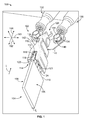
- Figure 1 is a perspective view of an electrical system 100 formed in accordance with one embodiment.
- the electrical system 100 and its various components are oriented with respect to mutually perpendicular axes 191-193 that include a mating axis 191, an elevation (or vertical) axis 192, and a lateral (or horizontal) axis 193.
- the elevation axis 192 may extend along a gravitational force direction, embodiments described herein are not required to have any particular orientation with respect to gravity.
- the electrical system 100 includes a power connector 102 and a conductive component 104 that is configured to deliver electrical power to the power connector 102 or receive electrical power from the power connector 102.
- the conductive component 104 has a substantially planar body that includes opposite sides 106, 108 and a leading edge 110.
- a uniform thickness T 1 of the conductive component 104 may extend between the sides 106, 108.
- the conductive component 104 may be a busbar.
- the conductive component 104 is oriented to extend along a plane that extends parallel to the mating and elevation axes 191, 192.
- the conductive component 104 may be another element that is capable of transmitting electrical power.
- the conductive component 104 may be one or more electrical contacts.
- the conductive component 104 may be configured to transmit, for example, at least 200 A.
- the power connector 102 includes an electrically insulative connector housing or shroud 112 having a mating end 114 and a contact cavity 116.
- the connector housing 112 has an opening or slot 118 at the mating end 114 that permits insertion of the conductive component 104 into the contact cavity 116.
- the power connector 102 also has a contact assembly 119 located within the contact cavity 116.
- the contact assembly 119 includes contact springs 120, 122 that are configured to electrically engage the conductive component 104.
- the contact springs 120, 122 are disposed within the contact cavity 116. More specifically, the contact springs 120, 122 are separated from each other with a receiving space 124 therebetween.
- the contact spring 120 is configured to engage the side 106
- the contact spring 122 is configured to engage the side 108.
- the contact springs 120, 122 are discrete elements that are mechanically joined together to engage the conductive component 104.
- the contact springs 120, 122 are electrically common.
- the term "discrete" means that the corresponding elements are distinct and separate elements.
- the contact springs 120, 122 are not shaped from a common piece of sheet material. Instead, each of the contact springs 120, 122 may be individually stamped-and -formed from sheet material and then subsequently joined. The joining operation may include, for example, forming a frictional engagement (e.g., interference fit, snap fit, and the like) to secure the contact springs 120, 122 to each other.
- the joining operation may be irreversible such that it would be necessary to damage the contact springs 120, 122 to separate them.
- the contact springs 120, 122 are neither joined with fastening hardware (e.g., screws, bolts, plugs, and the like) nor joined by melting/welding portions of the contact springs 120, 122 together.
- the leading edge 110 of the conductive component 104 is moved in an insertion direction I 1 along the mating axis 191 and advanced through the opening 118 and into the receiving space 124 between the contact springs 120, 122.
- the contact springs 120, 122 may engage the conductive component 104 and be deflected away from each other. More specifically, the contact springs 120, 122 may be deflected in opposite directions along the lateral axis 193.
- the contact springs 120, 122 slide along and press against the respective sides 106, 108.
- the conductive component 104 may engage the connector housing 112.
- the opening 118 may be shaped such that the connector housing 112 directs the conductive component 104 into a suitable orientation for engaging the contact springs 120, 122.
- the contact assembly 119 is configured to be electrically coupled to a power supply, such as power cables 130, 132.
- a power supply such as power cables 130, 132.
- the power connector 102 has a loading end 126 that is opposite the mating end 114.
- the contact springs 120, 122 have mounting portions 140, 142, respectively, that are located proximate to the loading end 126.
- the contact springs 120, 122 are coupled to the power cables 130, 132, respectively, at corresponding terminals 134, 136.
- the terminals 134, 136 are illustrated as ring terminals, although other types of terminals or methods for terminating may be used. More specifically, the terminals 134, 136 may be directly coupled to the mounting portions 140, 142, respectively.
- the terminals 134, 136 may be sandwiched between the respective mounting portion and a head 144 or other feature of a fastener 146.
- the power supply may be a circuit board, bus bar, or other component (not shown) to which the mounting portions 140, 142 are directly mounted.
- the power connector 102 has an offset right-angle configuration in which the mounting portions 140, 142 are mounted to a surface (not shown) that faces in a direction that is perpendicular to the insertion direction I 1 . More specifically, the mounting portions 140, 142 extend parallel to a plane defined by the mating and lateral axes 191, 193.
- the mounting portions may have an in-line configuration in which the mounting portions extend along or parallel to the plane defined by the mating and elevation axes 191, 192.
- the mounting portions may be oriented to extend parallel to a plane defined by the elevation and lateral axes 192, 193.
- FIG. 2 illustrates different stages 291-293 of manufacture of the contact springs 120, 122.
- a contact blank 200 is provided by stamping the contact blank 200 from conductive sheet material (not shown), such as sheet metal.
- the contact blank 200 has a first side surface 202, a second side surface 204, and an outer stamped edge 206 that extends between the first and second side surfaces 202, 204.
- the stamped edge 206 may include or define a thickness T 2 of the contact blank 200.
- a path of the stamped edge 206 forms a contact profile of the contact blank 200.
- the contact blank 200 includes unformed (e.g., non-shaped) portions of the contact springs 120, 122.
- the contact blank 200 includes a plurality of blank beams 210, a base feature 212, a mounting feature 214, and carrier standoffs 216, 218.
- portions of the stamped edge 206 may remain coupled or attached to other contact blanks 200 during manufacture of the contact springs. More specifically, multiple contact blanks 200 may be stamped from a single roll of sheet metal. The contact blanks 200 may remain attached to each other during at least one or more stages of manufacture.
- each of the contact springs 120, 122 may be formed from the contact blanks 200. More specifically, the contact springs 120, 122 may be formed from two contact blanks that have identical profiles. In alternative embodiments, however, the contact blank 200 may be configured to be formed into only one of the contact springs and the other contact spring may be formed from a contact blank (not shown) that has a different profile.
- the contact blank 200 may be shaped into either a partially-shaped contact blank 200A or a partially-shaped contact blank 200B.
- the contact blank 200A is further shaped and stamped to become the contact spring 120
- the contact blank 200B is further shaped and stamped to become the contact spring 122.
- the first and second side surfaces 202, 204 become outer and inner side surfaces 242, 244 of the contact spring 120.
- the first and second side surfaces 202, 204 become inner and outer side surfaces 222, 224.
- the carrier standoffs 216, 218 may include reference projections 217, 219.
- the reference projections 217, 219 may be used to facilitate maintaining the shape of the contact beams during the reeling process. However, the reference projections 217, 219 may be used for other purposes, such as facilitating the attachment of the connector housing 112 ( Figure 1 ) to the contact springs 120, 122 ( Figure 1 ).
- the contact spring 120 includes a contact body 260 having the opposite inner and outer side surfaces 244, 242 and a contact edge 262 that extends between the inner and outer side surfaces 244, 242.
- the contact body 260 is shaped to include a mating portion 264, a mounting portion 266, and a spring base 268 that joins the mating and mounting portions 264, 266.
- the contact spring 122 includes a contact body 270 having the opposite inner and outer side surfaces 222, 224 and a contact edge 272 that extends between the inner and outer side surfaces 222, 224.
- the contact body 270 is shaped to include a mating portion 274, a mounting portion 276, and a spring base 278 that joins the mating and mounting portions 274, 276.
- the spring bases 268 and 278 are configured to be mechanically joined to each other to interlock the contact springs 120, 122.
- the mating portions 264, 274 include contact fingers 230.
- the contact fingers 230 are shaped from the blank beams 210 and are configured to resiliently engage a corresponding side of the conductive component 104 ( Figure 1 ).
- a plating material may be applied to the blank beams 210 (or the contact fingers 230).
- the plating material is applied using a selective strip-plating process. For example, silver or other plating material may be applied to the inner side surfaces 222, 244 along the contact fingers 230 or, more specifically, distal ends 231 of the contact fingers 230.
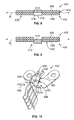
- Figures 3-5 illustrate cross-sectional views of the spring bases 278, 268 before, during, and after a joining operation, respectively.
- the joining operation creates a co-punched locking feature 308 (shown in Figure 5 ) that secures the spring bases 278, 268 together.
- the spring bases 278, 268 may be stacked side-by-side along an interface 305 as shown in Figure 3 .
- a gap is shown between the spring bases 278, 268 along the interface 305. It is understood, however, that the spring bases 278, 268 may directly abut each other along the interface 305 (e.g., as shown in Figures 4 and 5 ) prior to the joining operation. More specifically, the inner side surfaces 222, 244 may directly abut each other.
- the outer side surfaces 224, 242 face away from the interface 305.
- an interface plane P 1 extends between the spring bases 278, 268 along the interface 305.
- a punch element 310 may be positioned adjacent to the outer side surface 224 of the spring base 278.
- the punch element 310 has a circular cross-section, but other cross-sections may be used.
- the punch element 310 has an outer dimension D 1 , which can be a diameter of a circle in some embodiments.
- the punch element 310 is configured to deform a localized portion 312 of the spring base 278.
- the localized portion 312 is configured to engage a similarly sized localized portion 315 of the spring base 268 when the localized portion 312 is deformed by the punch element 310.
- the punch element 310 is driven (e.g., punched) in a punching direction Y 1 into the outer side surface 224 at the spring base 278 and toward the spring base 268.
- the localized portion 312 ( Figure 3 ) of the spring base 278 is deformed to create a body projection 314 that projects from the remainder of the spring base 278 (e.g., the portion of the spring base 278 that is not deformed by the punch element 310).
- the body projection 314 clears the interface plane P 1 .
- the body projection 314 also deforms the localized portion 315 ( Figure 3 ) of the spring base 268 to create a body projection 316 having a body recess 317.
- the body recess 317 is defined by the deformed portion of the inner side surface 244.
- a punching machine used to create the locking feature 308 may include an anvil 322 and movable arms 324, 326 that define a chamber 320.
- a die may also be located along the side surface 242 to support the spring bases 268, 278 during the punching process.
- a hole (not shown) in the die may permit the locking feature 308 to be punched therethrough.
- the localized portion 315 of the spring base 268 is driven into the chamber 320 when deformed by the punch element 310.
- the anvil 322 is located such that the outer side surface 242 engages the anvil 322.
- the movable arms 324, 326 are configured to permit the lateral deformation. More specifically, the arms 324, 326 are configured to move or rotate away from punch element 310 as indicated in Figure 4 .
- the body recess 317 defined by the inner side surface 244 of the spring base 268 has a recess opening 328 along the inner side surface 244.
- the body projection 314 has a distal punch profile 330 along the inner side surface 222. Due to the lateral deformation described above, the punch profile 330 is dimensioned greater than the recess opening 328. As such, the inner side surfaces 222, 244 frictionally engage each other to prevent removal of the body projection 314 from the body recess 317.
- locking feature 308 may include multiple co-punched locking features.
- the multiple locking features may be identical to each other in size and shape.
- the locking features may be different.
- the locking feature 308 is formed by deforming the localized portions 312, 315 in the punching direction Y 1 .
- one or more locking features may be formed by deforming other localized portions of the spring bases 278, 268 in a direction that is opposite the punching direction Y 1 .
- a plurality of co-punched locking features may have different dimensions with respect to each other.
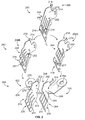
- FIG. 6 is an exploded view of the power connector 102.
- the joined contact springs 120, 122 constitute the contact assembly 119.
- the contact assembly 119 includes a plurality of the co-punched locking features 308A-308C.
- the spring bases 268, 278 when the spring bases 268, 278 are joined, the spring bases 268, 278 define a base seam 280 therebetween.
- the mating portions 264, 274 extend from the base seam 280 toward the distal ends 231 of the contact fingers 230.
- At least two of the locking features 308A, 308B are located proximate to the base seam 280.
- the locking features 308A, 308B are configured to prevent contact springs 120, 122 from separating.
- the contact fingers 230 of the mating portions 264, 274 are deflected away from each other by the conductive component 104.
- the locking features 308A, 308B are configured to prevent the spring bases 268, 278 from separating along the base seam 280.
- the contact cavity 116 of the connector housing 112 is dimensioned to receive the contact assembly 119.
- the contact cavity 116 is configured to receive the mating portions 264, 274 and the spring bases 268, 278.
- the connector housing 112 includes opposite sidewalls 282, 284 and a top wall 286 that extends between and joins the sidewalls 282, 284.
- the sidewalls 282, 284 include edges 283, 285, respectively, that define a cavity opening 288.
- the cavity opening 288 is dimensioned to receive the contact assembly 119 when the connector housing 112 is mounted onto the contact assembly 119.
- Figure 7 is a perspective view of the power connector 102. As shown, when the power connector 102 is assembled, the connector housing 112 is positioned over the mounting portions 266, 276. In the illustrated embodiment, the mounting portions 266, 276 project in opposite directions generally away from the connector housing 112. However, as discussed above, the mounting portions 266, 276 may be configured differently in alternative embodiments.
- the connector housing 112 is shaped relative to the contact assembly 119 to prevent movement of the connector housing 112 during a mating operation.
- the sidewalls 282, 284 may define channels 296, 298 (indicated in phantom in Figure 7 ).
- the channel 296 is sized and shaped to receive the locking features 308A, 308B when the connector housing 112 is mounted onto the contact assembly 119, and the channel 298 is sized and shaped to receive the locking feature 308C.
- the channels 296, 298 are defined by interior surfaces of the connector housing 112. In some embodiments, the interior surfaces may function as positive stops that prevent the connector housing 112 from moving in the insertion direction I 1 .
- the relative dimensions of the connector housing 112 and the locking features 308A-308C may prevent the connector housing 112 from moving with respect to the contact assembly 119.
- the reference projections 219 may also be configured to engage an edge (not shown) of the connector housing 112 and prevent moving in the insertion direction I 1 .
- Figures 8 and 9 illustrate cross-sections of contact springs 402, 404 before and after a joining operation, respectively.
- the contact springs 402, 404 may have similar features and elements as the contact springs 120, 122 ( Figure 1 ).
- the contact springs 402, 404 include spring bases 406, 408, respectively, that are positioned side-by-side along an interface 410.
- the interface 410 may extend along an interface plane P 2 .
- the joining operation is configured to create a locking feature 412 ( Figure 9 ).
- the spring base 406 includes a localized portion 414
- the spring base 408 includes a window or aperture 416 ( Figure 8 ) that is defined by an edge 418 ( Figure 8 ) (indicated by dashed lines).
- the localized portion 414 may be a tab that is stamped from the spring base 406.
- the localized portion 414 is bent into and through the window 416 such that the localized portion 414 clears the interface plane P 2 .
- the localized portion 414 When projecting through the window 416, the localized portion 414 may be referred to as a body projection.
- the localized portion 414 may be folded over the edge 418 to engage (e.g., grip) an outer side surface 420 of the spring base 408.
- Figure 10 is a perspective view of a contact assembly 422 that includes the contact springs 402, 404.
- the contact assembly 422 is configured to be received by a connector housing to form a power connector.
- the contact assembly 422 includes the locking feature 412 and also a locking feature 424 that is formed in a similar manner as the locking feature 412.
- the localized portion 414 extends through the window 416 and is folded over to engage the spring base 408.
- a localized portion 426 of the spring base 406 may be deformed to extend through a window 428 of the spring base 408 and folded over to engage the spring base 408. As shown, the localized portions 414, 426 are folded in opposite directions.
Landscapes
- Coupling Device And Connection With Printed Circuit (AREA)
- Engineering & Computer Science (AREA)
- Manufacturing & Machinery (AREA)
Applications Claiming Priority (1)
| Application Number | Priority Date | Filing Date | Title |
|---|---|---|---|
| US13/898,878 US9070990B2 (en) | 2013-05-21 | 2013-05-21 | Power connector having opposing contact springs |
Publications (1)
| Publication Number | Publication Date |
|---|---|
| EP2806499A1 true EP2806499A1 (de) | 2014-11-26 |
Family
ID=50685836
Family Applications (1)
| Application Number | Title | Priority Date | Filing Date |
|---|---|---|---|
| EP14168118.9A Withdrawn EP2806499A1 (de) | 2013-05-21 | 2014-05-13 | Leistungsverbinder mit gegenüberliegenden Kontaktfedern |
Country Status (3)
| Country | Link |
|---|---|
| US (1) | US9070990B2 (de) |
| EP (1) | EP2806499A1 (de) |
| CN (1) | CN104183940B (de) |
Cited By (2)
| Publication number | Priority date | Publication date | Assignee | Title |
|---|---|---|---|---|
| EP3206258A1 (de) * | 2016-02-10 | 2017-08-16 | Auto-Kabel Management GmbH | System zur herstellung einer elektrischen verbindung, elektrische verbindung und verfahren zu deren herstellung |
| CN114846700A (zh) * | 2019-12-20 | 2022-08-02 | 莫列斯有限公司 | 电连接器 |
Families Citing this family (18)
| Publication number | Priority date | Publication date | Assignee | Title |
|---|---|---|---|---|
| DE102013202513B4 (de) * | 2013-02-15 | 2023-04-27 | Te Connectivity Germany Gmbh | Elektrischer Verbinder |
| US9680236B2 (en) * | 2013-07-08 | 2017-06-13 | Fci Americas Technology Llc | Electrical connector |
| EP3051635B1 (de) * | 2015-01-30 | 2018-01-17 | TE Connectivity Germany GmbH | Elektrische Kontaktmittel und elektrische Kabelanordnung für die Automobilindustrie |
| DE102015216632A1 (de) * | 2015-08-31 | 2017-03-02 | Te Connectivity Germany Gmbh | Anordnung zum Herstellen einer elektrischen Verbindung zwischen einem Flachkontakt und einem Hochstromleiter |
| US10522945B2 (en) | 2016-08-22 | 2019-12-31 | Interplex Industries, Inc. | Electrical connector |
| WO2018039123A1 (en) | 2016-08-22 | 2018-03-01 | Interplex Industries, Inc. | Electrical connector |
| WO2018081722A1 (en) * | 2016-10-31 | 2018-05-03 | Haddock Dustin M M | Metal panel electrical bonding clip |
| CN106654608B (zh) * | 2017-03-01 | 2022-06-28 | 郭培囵 | 一种弹性电气连接器 |
| CN109326909A (zh) | 2018-11-20 | 2019-02-12 | 安费诺商用电子产品(成都)有限公司 | 一种高密度大功率卡类连接端子以及连接器 |
| US11177599B2 (en) * | 2019-01-28 | 2021-11-16 | TE Connectivity Services Gmbh | Power connector for a bus bar |
| CN110011092B (zh) * | 2019-03-22 | 2021-08-20 | 富士康(昆山)电脑接插件有限公司 | 电连接器 |
| TWI744854B (zh) | 2020-04-07 | 2021-11-01 | 大陸商東莞立訊技術有限公司 | 電連接器 |
| TWI739373B (zh) | 2020-04-07 | 2021-09-11 | 大陸商東莞立訊技術有限公司 | 電連接器 |
| CN113823934B (zh) * | 2020-06-19 | 2025-06-17 | 泰科电子(上海)有限公司 | 连接器和导电端子模组 |
| CN114520424A (zh) * | 2020-11-19 | 2022-05-20 | 中兴通讯股份有限公司 | 一种金手指连接器及其接电模块、电源柜 |
| CN214797803U (zh) * | 2020-12-30 | 2021-11-19 | 泰科电子(上海)有限公司 | 端子本体、连接端子及用于制作端子本体的片料 |
| US20230061609A1 (en) * | 2021-08-25 | 2023-03-02 | Hamilton Sundstrand Corporation | Electrical dual surface conductor lug |
| US12456828B2 (en) | 2021-10-18 | 2025-10-28 | Amphenol Commercial Products (Chengdu) Co., Ltd. | Hybrid card edge connector |
Citations (9)
| Publication number | Priority date | Publication date | Assignee | Title |
|---|---|---|---|---|
| DE1899448U (de) * | 1964-04-23 | 1964-08-27 | Siemens Ag | Federelement fuer steckverbindungen. |
| JPH11126554A (ja) * | 1997-08-20 | 1999-05-11 | Matsushita Electric Works Ltd | 接続変換アダプタ |
| US6280216B1 (en) * | 1999-11-09 | 2001-08-28 | General Electric Company | Lug adapter assembly having reduced force clips |
| JP2002063970A (ja) * | 2000-08-17 | 2002-02-28 | American Denki Co Ltd | 変換アダプター |
| US6358094B1 (en) * | 1999-09-15 | 2002-03-19 | Fci Americas Technology, Inc. | Low inductance connector with enhanced capacitively coupled contacts for power applications |
| WO2004021521A1 (en) * | 2002-08-27 | 2004-03-11 | Fci | Connection device including a contact surrounded by a spring |
| JP2004178940A (ja) * | 2002-11-26 | 2004-06-24 | Matsushita Electric Works Ltd | 速結端子装置並びに配線器具 |
| US20130012072A1 (en) * | 2011-07-07 | 2013-01-10 | Tyco Electronics Corporation | Electrical connectors having opposing electrical contacts |
| WO2013050299A1 (en) * | 2011-10-07 | 2013-04-11 | Tyco Electronics Amp Gmbh | Two-part crimp contact element |
Family Cites Families (8)
| Publication number | Priority date | Publication date | Assignee | Title |
|---|---|---|---|---|
| US5177861A (en) | 1980-09-08 | 1993-01-12 | Btm Corporation | Apparatus for joining sheet material |
| US5150513A (en) | 1980-09-08 | 1992-09-29 | Btm Corporation | Apparatus for joining sheet material |
| US4845589A (en) | 1987-05-04 | 1989-07-04 | Amp Incorporated | Bus bar connector assembly |
| US4878862A (en) | 1988-12-05 | 1989-11-07 | Amp Incorporated | Connector for mating two bus bars |
| US5618187A (en) | 1994-11-17 | 1997-04-08 | The Whitaker Corporation | Board mount bus bar contact |
| US6102754A (en) | 1997-03-31 | 2000-08-15 | The Whitaker Corporation | Bus bar contact |
| EP2048746B1 (de) * | 2007-08-13 | 2016-10-05 | Tyco Electronics Nederland B.V. | Stromschienenanschlusssystem |
| US7806711B2 (en) * | 2009-02-27 | 2010-10-05 | American Power Conversion Corporation | Electrical connector |
-
2013
- 2013-05-21 US US13/898,878 patent/US9070990B2/en active Active
-
2014
- 2014-05-13 EP EP14168118.9A patent/EP2806499A1/de not_active Withdrawn
- 2014-05-21 CN CN201410317092.6A patent/CN104183940B/zh active Active
Patent Citations (9)
| Publication number | Priority date | Publication date | Assignee | Title |
|---|---|---|---|---|
| DE1899448U (de) * | 1964-04-23 | 1964-08-27 | Siemens Ag | Federelement fuer steckverbindungen. |
| JPH11126554A (ja) * | 1997-08-20 | 1999-05-11 | Matsushita Electric Works Ltd | 接続変換アダプタ |
| US6358094B1 (en) * | 1999-09-15 | 2002-03-19 | Fci Americas Technology, Inc. | Low inductance connector with enhanced capacitively coupled contacts for power applications |
| US6280216B1 (en) * | 1999-11-09 | 2001-08-28 | General Electric Company | Lug adapter assembly having reduced force clips |
| JP2002063970A (ja) * | 2000-08-17 | 2002-02-28 | American Denki Co Ltd | 変換アダプター |
| WO2004021521A1 (en) * | 2002-08-27 | 2004-03-11 | Fci | Connection device including a contact surrounded by a spring |
| JP2004178940A (ja) * | 2002-11-26 | 2004-06-24 | Matsushita Electric Works Ltd | 速結端子装置並びに配線器具 |
| US20130012072A1 (en) * | 2011-07-07 | 2013-01-10 | Tyco Electronics Corporation | Electrical connectors having opposing electrical contacts |
| WO2013050299A1 (en) * | 2011-10-07 | 2013-04-11 | Tyco Electronics Amp Gmbh | Two-part crimp contact element |
Cited By (6)
| Publication number | Priority date | Publication date | Assignee | Title |
|---|---|---|---|---|
| EP3206258A1 (de) * | 2016-02-10 | 2017-08-16 | Auto-Kabel Management GmbH | System zur herstellung einer elektrischen verbindung, elektrische verbindung und verfahren zu deren herstellung |
| CN114846700A (zh) * | 2019-12-20 | 2022-08-02 | 莫列斯有限公司 | 电连接器 |
| EP4078736A4 (de) * | 2019-12-20 | 2024-01-10 | Molex, LLC | Elektrischer steckverbinder |
| US12237604B2 (en) | 2019-12-20 | 2025-02-25 | Molex, Llc | Electrical connector |
| CN114846700B (zh) * | 2019-12-20 | 2025-07-01 | 莫列斯有限公司 | 电连接器 |
| EP4657669A2 (de) | 2019-12-20 | 2025-12-03 | Molex, LLC | Elektrischer verbinder |
Also Published As
| Publication number | Publication date |
|---|---|
| CN104183940B (zh) | 2019-12-31 |
| US20140349529A1 (en) | 2014-11-27 |
| US9070990B2 (en) | 2015-06-30 |
| CN104183940A (zh) | 2014-12-03 |
Similar Documents
| Publication | Publication Date | Title |
|---|---|---|
| US9070990B2 (en) | Power connector having opposing contact springs | |
| JP5221313B2 (ja) | 端子金具 | |
| EP3018763B1 (de) | Steckverbinder | |
| US7241189B2 (en) | High-current terminal blade type connector | |
| US8342894B2 (en) | Terminal fitting | |
| US4776651A (en) | Socket contacts | |
| US10290990B2 (en) | Method for manufacturing female terminal and female terminal | |
| US9356367B2 (en) | Electrical connector having compliant contacts and a circuit board assembly including the same | |
| JP2005534142A (ja) | 電力コネクタ | |
| MX2007010678A (es) | Ensamble de canal transversal de montaje de superficie de dos piezas que tiene una superficie de alineacion plana. | |
| JPS603745B2 (ja) | 電気接続子 | |
| CN106532308A (zh) | 具有改进的连接凸部几何形状的金属片材零件 | |
| US11616316B2 (en) | Socket contact element for an electrically conductive connection | |
| US7513792B2 (en) | Chained-terminals body, method of manufacturing the same, and crimper for crimping the same | |
| JP2016149336A (ja) | ピン端子、端子群及びコネクタ | |
| US8341839B2 (en) | Method for producing terminals | |
| US10038293B2 (en) | Method of making electrical contact with contact area geometry enlargement | |
| JP2006179209A (ja) | 雌端子及びコネクタ | |
| KR20220098219A (ko) | 가이드 플레이트를 구비한 플러그 | |
| US20200185851A1 (en) | Terminal fitting | |
| JP4467099B2 (ja) | 電気コネクタの端子 | |
| MXPA06005721A (es) | Ensamble de colector para montaje en superficie. | |
| US4865567A (en) | Miniature barrel female terminal | |
| JP3196116B2 (ja) | シールド電気コネクタ及びその製法 | |
| JP2021057208A (ja) | 雄端子、および雄コネクタ |
Legal Events
| Date | Code | Title | Description |
|---|---|---|---|
| PUAI | Public reference made under article 153(3) epc to a published international application that has entered the european phase |
Free format text: ORIGINAL CODE: 0009012 |
|
| 17P | Request for examination filed |
Effective date: 20140513 |
|
| AK | Designated contracting states |
Kind code of ref document: A1 Designated state(s): AL AT BE BG CH CY CZ DE DK EE ES FI FR GB GR HR HU IE IS IT LI LT LU LV MC MK MT NL NO PL PT RO RS SE SI SK SM TR |
|
| AX | Request for extension of the european patent |
Extension state: BA ME |
|
| R17P | Request for examination filed (corrected) |
Effective date: 20150511 |
|
| RBV | Designated contracting states (corrected) |
Designated state(s): AL AT BE BG CH CY CZ DE DK EE ES FI FR GB GR HR HU IE IS IT LI LT LU LV MC MK MT NL NO PL PT RO RS SE SI SK SM TR |
|
| RAP1 | Party data changed (applicant data changed or rights of an application transferred) |
Owner name: TE CONNECTIVITY CORPORATION |
|
| 17Q | First examination report despatched |
Effective date: 20170315 |
|
| GRAP | Despatch of communication of intention to grant a patent |
Free format text: ORIGINAL CODE: EPIDOSNIGR1 |
|
| RIC1 | Information provided on ipc code assigned before grant |
Ipc: H01R 43/16 20060101ALN20181115BHEP Ipc: H01R 13/11 20060101ALI20181115BHEP Ipc: H01R 4/10 20060101AFI20181115BHEP |
|
| INTG | Intention to grant announced |
Effective date: 20181206 |
|
| STAA | Information on the status of an ep patent application or granted ep patent |
Free format text: STATUS: THE APPLICATION IS DEEMED TO BE WITHDRAWN |
|
| 18D | Application deemed to be withdrawn |
Effective date: 20190417 |