EP2806473B1 - Organische lichtemittierende Anzeigevorrichtung mit einem flexiblen Substrat - Google Patents
Organische lichtemittierende Anzeigevorrichtung mit einem flexiblen Substrat Download PDFInfo
- Publication number
- EP2806473B1 EP2806473B1 EP14168669.1A EP14168669A EP2806473B1 EP 2806473 B1 EP2806473 B1 EP 2806473B1 EP 14168669 A EP14168669 A EP 14168669A EP 2806473 B1 EP2806473 B1 EP 2806473B1
- Authority
- EP
- European Patent Office
- Prior art keywords
- layer
- organic light
- plastic
- barrier layer
- emitting device
- Prior art date
- Legal status (The legal status is an assumption and is not a legal conclusion. Google has not performed a legal analysis and makes no representation as to the accuracy of the status listed.)
- Active
Links
Images



Classifications
-
- H—ELECTRICITY
- H10—SEMICONDUCTOR DEVICES; ELECTRIC SOLID-STATE DEVICES NOT OTHERWISE PROVIDED FOR
- H10K—ORGANIC ELECTRIC SOLID-STATE DEVICES
- H10K77/00—Constructional details of devices covered by this subclass and not covered by groups H10K10/80, H10K30/80, H10K50/80 or H10K59/80
- H10K77/10—Substrates, e.g. flexible substrates
- H10K77/111—Flexible substrates
-
- H—ELECTRICITY
- H10—SEMICONDUCTOR DEVICES; ELECTRIC SOLID-STATE DEVICES NOT OTHERWISE PROVIDED FOR
- H10K—ORGANIC ELECTRIC SOLID-STATE DEVICES
- H10K50/00—Organic light-emitting devices
- H10K50/80—Constructional details
- H10K50/84—Passivation; Containers; Encapsulations
- H10K50/844—Encapsulations
-
- H—ELECTRICITY
- H10—SEMICONDUCTOR DEVICES; ELECTRIC SOLID-STATE DEVICES NOT OTHERWISE PROVIDED FOR
- H10K—ORGANIC ELECTRIC SOLID-STATE DEVICES
- H10K50/00—Organic light-emitting devices
- H10K50/80—Constructional details
- H10K50/84—Passivation; Containers; Encapsulations
- H10K50/844—Encapsulations
- H10K50/8445—Encapsulations multilayered coatings having a repetitive structure, e.g. having multiple organic-inorganic bilayers
-
- H—ELECTRICITY
- H10—SEMICONDUCTOR DEVICES; ELECTRIC SOLID-STATE DEVICES NOT OTHERWISE PROVIDED FOR
- H10K—ORGANIC ELECTRIC SOLID-STATE DEVICES
- H10K59/00—Integrated devices, or assemblies of multiple devices, comprising at least one organic light-emitting element covered by group H10K50/00
- H10K59/10—OLED displays
- H10K59/12—Active-matrix OLED [AMOLED] displays
- H10K59/1201—Manufacture or treatment
-
- H—ELECTRICITY
- H10—SEMICONDUCTOR DEVICES; ELECTRIC SOLID-STATE DEVICES NOT OTHERWISE PROVIDED FOR
- H10K—ORGANIC ELECTRIC SOLID-STATE DEVICES
- H10K59/00—Integrated devices, or assemblies of multiple devices, comprising at least one organic light-emitting element covered by group H10K50/00
- H10K59/80—Constructional details
- H10K59/87—Passivation; Containers; Encapsulations
- H10K59/873—Encapsulations
-
- H—ELECTRICITY
- H10—SEMICONDUCTOR DEVICES; ELECTRIC SOLID-STATE DEVICES NOT OTHERWISE PROVIDED FOR
- H10K—ORGANIC ELECTRIC SOLID-STATE DEVICES
- H10K71/00—Manufacture or treatment specially adapted for the organic devices covered by this subclass
-
- H—ELECTRICITY
- H10—SEMICONDUCTOR DEVICES; ELECTRIC SOLID-STATE DEVICES NOT OTHERWISE PROVIDED FOR
- H10K—ORGANIC ELECTRIC SOLID-STATE DEVICES
- H10K2102/00—Constructional details relating to the organic devices covered by this subclass
- H10K2102/301—Details of OLEDs
- H10K2102/311—Flexible OLED
-
- H—ELECTRICITY
- H10—SEMICONDUCTOR DEVICES; ELECTRIC SOLID-STATE DEVICES NOT OTHERWISE PROVIDED FOR
- H10K—ORGANIC ELECTRIC SOLID-STATE DEVICES
- H10K59/00—Integrated devices, or assemblies of multiple devices, comprising at least one organic light-emitting element covered by group H10K50/00
- H10K59/10—OLED displays
- H10K59/12—Active-matrix OLED [AMOLED] displays
-
- H—ELECTRICITY
- H10—SEMICONDUCTOR DEVICES; ELECTRIC SOLID-STATE DEVICES NOT OTHERWISE PROVIDED FOR
- H10K—ORGANIC ELECTRIC SOLID-STATE DEVICES
- H10K59/00—Integrated devices, or assemblies of multiple devices, comprising at least one organic light-emitting element covered by group H10K50/00
- H10K59/80—Constructional details
- H10K59/87—Passivation; Containers; Encapsulations
- H10K59/873—Encapsulations
- H10K59/8731—Encapsulations multilayered coatings having a repetitive structure, e.g. having multiple organic-inorganic bilayers
-
- Y—GENERAL TAGGING OF NEW TECHNOLOGICAL DEVELOPMENTS; GENERAL TAGGING OF CROSS-SECTIONAL TECHNOLOGIES SPANNING OVER SEVERAL SECTIONS OF THE IPC; TECHNICAL SUBJECTS COVERED BY FORMER USPC CROSS-REFERENCE ART COLLECTIONS [XRACs] AND DIGESTS
- Y02—TECHNOLOGIES OR APPLICATIONS FOR MITIGATION OR ADAPTATION AGAINST CLIMATE CHANGE
- Y02E—REDUCTION OF GREENHOUSE GAS [GHG] EMISSIONS, RELATED TO ENERGY GENERATION, TRANSMISSION OR DISTRIBUTION
- Y02E10/00—Energy generation through renewable energy sources
- Y02E10/50—Photovoltaic [PV] energy
- Y02E10/549—Organic PV cells
-
- Y—GENERAL TAGGING OF NEW TECHNOLOGICAL DEVELOPMENTS; GENERAL TAGGING OF CROSS-SECTIONAL TECHNOLOGIES SPANNING OVER SEVERAL SECTIONS OF THE IPC; TECHNICAL SUBJECTS COVERED BY FORMER USPC CROSS-REFERENCE ART COLLECTIONS [XRACs] AND DIGESTS
- Y02—TECHNOLOGIES OR APPLICATIONS FOR MITIGATION OR ADAPTATION AGAINST CLIMATE CHANGE
- Y02P—CLIMATE CHANGE MITIGATION TECHNOLOGIES IN THE PRODUCTION OR PROCESSING OF GOODS
- Y02P70/00—Climate change mitigation technologies in the production process for final industrial or consumer products
- Y02P70/50—Manufacturing or production processes characterised by the final manufactured product
Definitions
- the present invention relates to an organic light-emitting display apparatus, and more particularly, to an organic light-emitting display apparatus including a flexible substrate.
- An organic light-emitting display apparatus generally includes a hole injection electrode, an electron injection electrode, and an organic light-emitting layer formed there between.
- the organic light-emitting display apparatus is a self light-emitting display apparatus that emits light when holes injected from the hole injection electrode and electrons injected from the electron injection electrode recombine within the organic light-emitting layer giving rise to an excited state that gradually dissipates thereafter.
- the organic light-emitting display apparatus Because of its high quality characteristics such as low power consumption, high brightness, and fast response speed, the organic light-emitting display apparatus has received attention as a next generation display.
- the organic light-emitting display apparatus includes a heavy and fragile glass substrate, characteristics such as portability and large size of the screen display are limited. Therefore, a flexible organic light-emitting display apparatus including a light and shock-resistant flexible substrate such as a plastic substrate has been developed recently.
- the organic light-emitting layer may be left vulnerable to moisture or oxygen and degradation may occur.
- US2002140347 discloses a flexible substrate layer; and a plurality of cooperative barrier layers disposed on the substrate layer.
- the plurality of cooperative barrier layers further comprise one or more planarizing layers and one or more high-density layers.
- US2005116637 discloses an organic electroluminescence display panel that includes an organic electroluminescence element and a resin substrate that supports the organic electroluminescence element.
- a gas barrier laminate is formed between the resin substrate and the organic electroluminescence element.
- EP2091096 discloses a capsulated electronic device comprising: a first barrier structure comprising at least one inorganic and at least one organic layer, a second barrier structure (30) comprising at least one inorganic and at least one organic layer, and an electronic device arranged between the first and the second barrier structure.
- US2012/0223350 discloses an OLED device having a flexible substrate with a barrier layer incorporated therein.
- KR10-2011-0133881 discloses a flexible board for an OLED display device wherein the board comprising a first plastic layer, a patterned barrier layer and a second plastic layer.
- Embodiments of the present invention may provide an organic light-emitting display apparatus including a flexible substrate with a low water vapor transmission rate and increased adhesive strength, and a method of manufacturing the organic light-emitting display apparatus.
- an organic light-emitting display apparatus as set out in claim 1.
- Preferred features are set out in claims 2 to 5.
- an electronic device as set out in claim 6.
- FIG. 1 is a cross-sectional view illustrating an organic light-emitting display apparatus according to an exemplary embodiment of the present invention.
- the organic light-emitting display apparatus 100 includes a flexible substrate FS, a thin film transistor (TFT) layer 110, an organic light-emitting device layer 120, and a thin film encapsulating layer 130.
- TFT thin film transistor
- the flexible substrate FS includes a first plastic layer 1PL, a first barrier layer 1BL, a second plastic layer 2PL, and a second barrier layer 2BL.
- the first plastic layer 1PL and the second plastic layer 2PL may be formed of a plastic material with excellent heat resistance and durability, for example, polyiminde, polyethylene naphthalate, polyethyleneterephthalate (PET), Polyarylate, polycarbonate, Polyetherimide (PEI), or Polyethersulfone.
- a plastic material with excellent heat resistance and durability for example, polyiminde, polyethylene naphthalate, polyethyleneterephthalate (PET), Polyarylate, polycarbonate, Polyetherimide (PEI), or Polyethersulfone.
- the plastic material for the first plastic layer 1PL and the second plastic layer 2PL transmits moisture or oxygen easily when compared to a glass substrate, an organic light-emitting layer vulnerable to moisture or oxygen is easily deteriorated, so that the lifecycle of the organic light-emitting display apparatus is reduced.
- the first barrier layer 1BL is formed on the first plastic layer 1PL
- the second barrier layer 2BL is formed on the second plastic layer 2PL.
- Each of the first barrier layer 1BL and the second barrier layer 2BL may be formed of an inorganic material, for example, metal oxide, silicon nitride, or silicon oxide.
- each of the first barrier layer 1BL and the second barrier layer 2BL may include a single layer or a multilayer formed of an inorganic material such as Al 2 O 3 , SiO 2 , and SiN x .
- Each of the first barrier layer 1BL and the second barrier layer 2BL formed of a single layer or a multilayer may have a water vapor transmission rate (WVTR) of less than about 10 g/m 2 day to about 5 g/m 2 day.
- WVTR water vapor transmission rate
- the first barrier layer 1BL is patterned to have an island shape.
- the first barrier layer 1BL is patterned to be located in an area A corresponding to the organic light-emitting device layer 120.
- the first plastic layer 1PL and the second plastic layer 2PL are in direct contact in a peripheral area B of the area A corresponding to the organic light-emitting device layer 120.
- the patterned first barrier layer 1BL may prevent the delamination between the first barrier layer 1BL and the second plastic layer 2PL.
- the first barrier layer 1BL is formed to overlap with the organic light-emitting device layer 120 without extending beyond the organic light-emitting device layer 120, while the second barrier layer 2BL is formed to extend beyond the organic light-emitting device layer 120.
- the TFT layer 110 and the organic light-emitting device layer 120 are formed on the flexible substrate FS.
- FIG. 2 is an enlarged view of a portion II of FIG. 1 , for example, a portion of the TFT layer 110 and the organic light-emitting device layer 120 of the organic light-emitting display apparatus 100.
- a TFT including a semiconductor layer 111, a gate electrode 113, a source electrode 115, and a drain electrode 116 may be formed on the second barrier layer 2BL.
- a gate insulating layer 112 may be formed between the semiconductor layer 111 and the gate electrode 113, and an interlayer insulating layer 114 may be formed between the gate electrode 113 and the source electrode 115 and between the gate electrode 113 and the drain electrode 116.
- the semiconductor layer 111 may be a poly-silicon TFT, an amorphous silicon TFT, an organic TFT, or a conductive oxide TFT.
- a top gate TFT is shown in FIG. 2 , embodiments of the present invention are not limited thereto. For example, various structures of TFTs including a bottom gate TFT may be applicable.
- a TFT is directly formed on the second barrier layer 2BL as shown in FIG. 2
- the present invention is not limited thereto.
- a buffer layer (not shown) may be further provided between the second barrier layer 2BL and the TFT.
- the buffer layer flattens the flexible substrate FS and prevents impurity elements from penetrating from the flexible substrate FS into the semiconductor layer 111.
- the buffer layer (not shown) may be a single layer or a multilayer of silicon nitride and/or silicon oxide.
- at least one capacitor may be connected to the TFT.
- a passivation layer 117 may be formed on the TFT and a pixel definition layer 122 may be formed on the passivation layer 117.
- the passivation layer 117 protects the TFT and flattens a top side of the TFT.
- An organic light-emitting device OLED may be connected to one of the source electrode 115 and the drain electrode 116 of the TFT.
- the organic light-emitting device OLED includes a pixel electrode 121, an opposite electrode 124, and a layer 123 including at least an organic light-emitting layer interposed between the pixel electrode 121 and the opposite electrode 124.
- the layer 123 including an organic light-emitting layer may be formed of a low molecular or polymer organic matter. When a low molecular organic matter is used, a hole injection layer (HIL), a hole transport layer (HTL), an emission layer (EML), an electron transport layer (ETL), and an electron injection layer (EIL) may be stacked in a single or complex structure.
- HIL hole injection layer
- HTL hole transport layer
- EML emission layer
- ETL electron transport layer
- EIL electron injection layer
- a structure including an HTL and an EML may be provided.
- the layer 123 including an organic light-emitting layer sub pixels emitting red, green, and blue light may form one unit pixel.
- the layer 123 including an organic light-emitting layer is formed by vertically stacking or mixing layers including light-emitting materials emitting red, green, and blue light.
- white light is emitted, a combination of other colors is possible. Additionally, a color conversion layer or a color filter converting the emitted white light into a predetermined color may be provided further.
- the opposite electrode 124 may be commonly formed in a plurality of pixels. For example, various modifications are possible.
- the pixel electrode 121 may function as an anode and the opposite electrode 124 may function as a cathode. However, the opposite may be possible too. Additionally, at least one of the pixel electrode 121 and the opposite electrode 124 may be provided as a transparent electrode through which a light emitted from a light-emitting layer passes.
- the organic light-emitting device layer 120 is formed on the TFT layer 100 as shown in FIGS. 1 and 2 , this is for concise description and other arrangements may be used. For example, a potion of the TFT layer 110 and the organic light-emitting device layer 120 may be formed on the same layer. For example, the gate electrode of the TFT and the pixel electrode of the organic light-emitting device OLED may be formed on the same layer.
- the thin film encapsulating layer 130 encapsulating the organic light-emitting device OLED is formed on the flexible substrate FS.
- the thin film encapsulating layer 130 may be formed of a plurality of inorganic layers or a mixture of an inorganic layer and an organic layer.
- the organic layer is formed of polymer, and may be a single layer or a stacked layer formed of one of polyethyleneterephthalate, polyimide, polycarbonate, epoxy, polyethylene, and polyacrylate.
- the organic layer may be formed of polyacrylate.
- the organic layer may include a polymerized monomer composition including diacrylate based monomer and triacrylate based monomer.
- the monomer composition may further include monoacrylate based monomer.
- the monomer composition may further include a well-known photo initiator such as TPO but is not limited thereto.
- the inorganic layer may be a single layer or a stacked layer including metal oxide or metal nitride.
- the organic layer may include SiN x , Al 2 O 3 , SiO 2 , or TiO 2 .
- the uppermost layer exposed to the outside in the thin film encapsulating layer 130 may be formed of an inorganic layer to prevent water and vapor transmission with respect to the organic light-emitting device OLED.
- the thin film encapsulating layer 130 may include at least one sandwich structure in which at least one organic layer is inserted between at least two inorganic layers. Additionally, the thin film encapsulating layer 130 may include at least one sandwich structure in which at least one inorganic layer is inserted between at least two organic layers.
- the thin film encapsulating layer 130 may include a first inorganic layer, a first organic layer, and a second inorganic layer, which are sequentially stacked on the organic light-emitting device OLED. Moreover, the thin film encapsulating layer 130 may include a first inorganic layer, a first organic layer, a second inorganic layer, a second organic layer, and a third inorganic layer, which are sequentially stacked on the organic light-emitting device OLED.
- the thin film encapsulating layer 130 may include a first inorganic layer, a first organic layer, a second inorganic layer, a second organic layer, a third inorganic layer, a third organic layer, and a fourth inorganic layer, which are sequentially stacked on the organic light-emitting device OLED.
- a halogenated metal layer including LiF may be additionally included between the organic light-emitting device OLED and the first inorganic layer.
- the halogenated metal layer may prevent the organic light-emitting device OLED from being damaged when the first inorganic layer is formed through a sputtering method or a plasma deposition method.
- the first organic layer may have a narrower area than the second inorganic layer, and the second organic layer may have a narrower area than the third inorganic layer.
- the first organic layer may be completely covered by the second inorganic layer.
- the second organic layer may be completely covered by the third inorganic layer.
- the thin film encapsulating layer 130 is directly formed on the opposite electrode 124 as shown in FIGS. 1 and 2 , this is just exemplary. Thus, other components such as fillers and adhesives may be further interposed between the opposite electrode 124 and the thin film encapsulating layer 130.
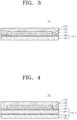
- FIG. 3 is a cross-sectional view illustrating an organic light-emitting display apparatus 101 according to a comparative example.
- the organic light-emitting display apparatus 101 includes a flexible substrate FS-1, a TFT layer 110, an organic light-emitting device layer 120, and a thin film encapsulating layer 130.
- the flexible substrate FS-1 includes a first plastic layer 1PL and a first barrier layer 1BL.
- the flexible substrate FS-1 includes a single plastic layer and a single barrier layer.
- the flexible substrate FS-1 includes the single plastic layer and the single barrier layer like in the first comparative example, damages such as cracks occur in the first barrier layer 1BL due to foreign materials or dent defects in the first plastic layer 1PL and/or the first barrier layer 1BL. Since moisture or oxygen is transmitted through such a damaged surface, defective organic light-emitting device OLEDs may be manufactured.
- FIG. 4 is a cross-sectional view illustrating an organic light-emitting display apparatus 102 according to a comparative example of the present invention.
- the organic light-emitting display apparatus 102 includes a flexible substrate FS-2, a TFT layer 110, an organic light-emitting device layer 120, and a thin film encapsulating layer 130.
- the flexible substrate FS-2 includes a first plastic layer 1PL, a first barrier layer 1BL, a second plastic layer 2PL, and a second barrier layer 2BL.
- the flexible substrate FS-2 includes two structures, each including a plastic layer and a barrier layer on the plastic layer.
- the water and vapor transmission power are improved by the flexible substrate FS-2 of the second comparative example improved, and thus, less dark spots occur.
- an adhesive strength (peel strength) between the first barrier layer 1BL of an inorganic layer and the second plastic layer 2PL of an organic layer is relatively weak, the first barrier layer 1BL and the second plastic layer 2PL are delaminated from each other during manufacturing processes.
- the organic light-emitting display apparatus 100 since the organic light-emitting display apparatus 100 according to an exemplary embodiment of the present invention includes the first barrier layer 1BL patterned to have an island shape, the first plastic layer 1PL and the second plastic layer 2PL are in direct contact in the peripheral area B of the area A corresponding to the organic light-emitting device layer 120 having no first barrier layer 1BL. Since an adhesive strength between the first plastic layer 1PL and the second plastic layer 2PL is greater than that between the first barrier layer 1BL and the second plastic layer 2PL, the delamination between the first barrier layer 1BL and the second plastic layer 2PL may be prevented by patterning the first barrier layer 1BL to have an island shape.
- the first barrier layer 1BL in an area corresponding to the organic light-emitting device layer 120, moisture and oxygen are prevented from penetrating from the first plastic layer 1PL into the organic light-emitting device layer 120 directly.
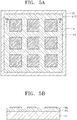
- FIGS. 5A to 11 are views illustrating a method of manufacturing the organic light-emitting display apparatus 100 according to an exemplary embodiment of the present invention.
- FIG. 5A is a plan view illustrating a process of forming a first plastic layer 1PL and a first barrier layer 1BL of a mother flexible substrate MFS on a glass substrate GS.
- FIG. 5B is a cross-sectional view taken along a line VB-VB of FIG. 5A .
- the mother flexible substrate MFS formed of plastic material bends or elongates when heat is applied thereto, it is difficult to accurately form thin film patterns such as various electrodes or conductive wires on the mother flexible substrate MFS. Also, several thin film pattern forming processes are performed when the mother flexible substrate MFS is bonded to the glass substrate GS, for example, a carrier substrate.
- the first plastic layer 1PL is formed on the glass substrate GS.
- the first plastic layer 1PL may be formed when a plastic polymer solution including at least one of polyimide, polyethylene naphthalate, PET, Polyarylate, polycarbonate, PEI, and Polyethersulfone is coated on the glass substrate GS and then hardened or a polymer film is laminated on the glass substrate GS.
- the first barrier layer 1BL patterned to have an island shape is formed on the first plastic layer 1PL. Hence, in this embodiment, a plurality of islands of the first barrier layer are formed.
- the first barrier layer 1BL may include a single layer or a multilayer, which are formed of an inorganic material such as AlO 3 , SiO 2 , or SiN x through chemical vapor deposition (CVD), plasma enhanced chemical vapor deposition (PECVD) or Atomic Layer Deposition (ALD).
- CVD chemical vapor deposition
- PECVD plasma enhanced chemical vapor deposition
- ALD Atomic Layer Deposition
- each island of the first barrier layer 1BL is formed to overlap with the corresponding organic light-emitting device layer 120 without extending beyond the organic light-emitting device layer 120, while the second barrier layer 2BL is formed to extend across all the organic light-emitting device layers 120.
- FIG. 6A is a plan view illustrating a process of forming a second plastic layer 2PL and a second barrier layer 2BL of a mother flexible substrate MFS on a glass substrate GS.
- FIG. 6B is a cross-sectional view taken along a line VIB-VIB of FIG. 6A .
- the second plastic layer 2PL is formed on the first barrier layer 1BL that is patterned.
- the second plastic layer 2PL may be formed of the same material and by the same method as the first plastic layer 1PL.
- the second plastic layer 2PL may alternatively be formed of a solution having lower viscosity than the first plastic layer 1PL.
- first and second plastic layers 1PL and 2PL are formed through coating, since a high viscosity coating solution has a lot of foreign materials, the first and second plastic layers 1PL and 2PL are coated with the foreign materials simultaneously during coating. Accordingly, since the second plastic layer 2PL is formed of a solution having lower viscosity than the first plastic layer 1PL, filtering may be possible during the coating of the second plastic layer 2PL. At this point, since the plastic layer 2PL is formed of a filtered material, the presence of foreign materials in the plastic layer 2PL may be reduced. Also, since a coating liquid used for forming the second plastic layer 2PL has a low concentration, the coating liquid may cover foreign materials occurring in the first plastic layer 1PL and the first barrier layer 1BL.
- each of the first plastic layer 1PL and the second plastic layer 2PL has the same thickness as shown in FIGS. 1 and 6B , the present invention is not limited thereto.
- the transmission time of oxygen and moisture from the outside of the flexible substrate FS is further affected by the thickness of the second plastic layer 2PL that is closer to the organic light-emitting device layer 120 than the first plastic layer 1PL.
- the thicker second plastic layer 2PL that is closer to the organic light-emitting device layer 120 than the first plastic layer, the water and vapor transmission time is delayed so that the deterioration of the OLED may be prevented.
- the second barrier layer 2BL is formed on the second plastic layer 2PL.
- the second barrier layer 2BL may be formed of the same material and by the same method as the first barrier layer 1BL.
- the second barrier layer 2BL is formed as a continuous layer, rather than as a plurality of islands.
- FIG. 7A is a plan view illustrating a process of forming a plurality of unit organic light-emitting display apparatus 100 on a mother flexible substrate MFS.
- FIG. 7B is a cross-sectional view taken along a line VIIB-VIIB of FIG. 7A .
- the plurality of unit organic light-emitting display apparatus 100 including a TFT layer 110 and an organic light-emitting device layer 120 are formed on the mother flexible substrate MFS.
- the plurality of unit organic light-emitting display apparatus 100 may be formed through a deposition method such as a PECV method, an atmospheric pressure CVD (APCVD), or a lower pressure CVD (LPCVD).
- a deposition method such as a PECV method, an atmospheric pressure CVD (APCVD), or a lower pressure CVD (LPCVD).
- APCVD atmospheric pressure CVD
- LPCVD lower pressure CVD
- the plurality of unit organic light-emitting display apparatus 100 may be formed a method such as coating or printing.
- polycrystalline silicon is used for forming the semiconductor layer 111 of FIG.
- amorphous silicon may be crystallized by applying various crystallization methods such as rapid thermal annealing (RTA), solid phase crystallization (SPC), excimer laser annealing (ELA), metal induced crystallization (MIC), metal induced lateral crystallization (MILC), and sequential lateral solidification (SLS).
- RTA rapid thermal annealing
- SPC solid phase crystallization
- ELA excimer laser annealing
- MIC metal induced crystallization
- MILC metal induced lateral crystallization
- SLS sequential lateral solidification
- the gate electrode 113 of FIG. 2 , the source electrode 115 of FIG. 2 , the drain electrode 116 of FIG. 2 , a capacitor (not shown), and various wires (not shown) are deposited on the TFT layer 110 through a method such as CVD, PECVD, or ALD, and then, a desired pattern is formed through a photolithography process.
- the layer 123 of FIG. 2 including an organic light-emitting material of the organic light-emitting device layer 120 may be formed through various methods such as a deposition method, a coating method, a printing method, and an optical-thermal transfer method.
- a buffer layer (not shown) may be further provided between the second barrier layer 2BL and the TFT layer 110.
- FIG. 8 is a cross-sectional view illustrating a process of forming a thin film encapsulating layer 130 encapsulating a plurality of organic light-emitting device layers 120 on the mother flexible substrate MFS.
- the thin film encapsulating layer 130 may be formed of a plurality of inorganic layers or a mixture of an inorganic layer and an organic layer.
- the inorganic layer and the organic layer may be formed through various methods such as CVD, PECVD, and sputtering.
- one thin film encapsulating layer 130 is commonly covers the plurality of unit organic light-emitting display apparatus 100 overall as shown in FIG. 8 , the present invention is not limited thereto. That is, the thin film encapsulating layer 130 may be discontinuously formed to separately cover each unit organic light-emitting device of the organic light-emitting display apparatus 100.
- FIGS. 9 and 10 are cross-sectional views illustrating a process of separating a glass substrate GS from a mother flexible substrate MFS.
- a laser beam is radiated from an opposite direction of a side where the mother flexible substrate MFS is formed.
- the laser beam may an UV light radiated by using an excimer laser device.
- the radiated UV light passes through the glass substrate GS and is absorbed by the first plastic layer 1PL and the second plastic layer 2PL.
- An adhesive strength between the first plastic layer 1PL and the second plastic layer 2PL becomes weaker due to the absorbed energy.
- the second barrier layer 2BL is easily broken by external tension. Accordingly, by properly applying an external tension in an arrow direction of FIG. 10 to the mother flexible substrate MFS and the glass substrate GS, the mother flexible substrate MFS may be separated from the glass substrate GS.
- the first barrier layer 1BL and the second plastic layer 2PL can be delaminated from each other during manufacturing processes.
- the first barrier layer 1BL may be patterned to have an island shape only in an area A corresponding to the organic light-emitting device layer 120, the first plastic layer 1PL and the second plastic layer 2PL are in direct contact in the peripheral area B of the area A corresponding to the organic light-emitting device layer 120 having no first barrier layer 1BL. Since an adhesive strength between the first plastic layer 1PL and the second plastic layer 2PL is greater than that between the first barrier layer 1BL and the second plastic layer 2PL, the delamination between the first barrier layer 1BL and the second plastic layer 2PL may be prevented.
- a first protective film 140 may be attached on the thin film encapsulating layer 130 prior to a process of separating the mother flexible substrate MFS from the glass substrate GS.
- the first protective film 140 may be used as an optical member such as a polarizing film.
- FIG. 11 is a cross-sectional view illustrating a process of dividing an organic light-emitting device layer on a mother flexible substrate MFS into a plurality of unit display devices 100.
- the second protective film 150 may be used as an optical member such as a polarizing film.
- an organic light-emitting device layer formed on the mother flexible substrate MFS may be divided into a plurality of unit display devices 100.
- a method of manufacturing a mother flexible substrate MFS-2 of an organic light-emitting display apparatus 102 according to a comparative example of the present invention will be described with reference to FIGS. 12A and 12B .
- FIG. 12A is a plan view illustrating a process of forming a mother flexible substrate MFS-2 on a glass substrate GS.
- FIG. 12B is a cross-sectional view taken along a line XIIB-XIIB of FIG. 12A.
- FIGS. 12A and 12B also illustrate an outer part of a contact surface of the glass substrate GS and the mother flexible substrate MFS-2.
- the first plastic layer 1PL and the second plastic layer 2PL on the glass substrate GS are covered by the first barrier layer 1BL and the second barrier layer 2BL, respectively.
- the first barrier layer 1BL is not patterned.
- the first plastic layer 1PL and the second plastic layer 2PL are formed on the glass substrate GS through a coating process, if a coating liquid flows to the outside of the glass substrate GS, defects occur. Accordingly, the first plastic layer 1PL and the second plastic layer 2PL may be coated in a smaller area than the glass substrate GS.
- the first barrier layer 1BL and the second barrier layer 2BL are formed through a deposition process such as CVD or PECVE, they are closer to an end part of the glass substrate GS than the first plastic layer 1PL and the second plastic layer 2PL.
- the second plastic layer 2PL covers a portion of the first plastic layer 1PL. Accordingly, even when the second plastic layer 2PL and the first plastic layer 1PL are formed at the same position, and the second plastic layer 2PL flows to the outer part of the first plastic layer 1PL due to a flowing coating liquid.
- An area OA where a first barrier layer 1BL-1 and a second plastic layer 2PL overlap is formed in an outer part of the mother flexible substrate MFS-2.
- a radiated UV light passes through the glass substrate GS and is absorbed by the first plastic layer 1PL and the second plastic layer 2PL.
- the first barrier layer 1BL absorbs the UV light in the area OA where the first barrier layer 1BL and the second plastic layer 2PL overlap, the UV light is not absorbed by the second plastic layer 2PL.
- FIG. 13 is a detailed view illustrating an outer part of a contact surface of the glass substrate GS and the mother flexible substrate MFS.
- the first barrier layer 1BL is not formed in an outer part of the glass substrate GS
- an area OA where the first barrier layer 1BL and the second plastic layer 2PL overlap is not formed in an outer part of the mother flexible substrate MFS.
- an end part of the second plastic layer 2PL and an end part of the first barrier layer 1BL are in direct contact at an end part of the glass substrate GS. Accordingly, a separation process of the mother flexible substrate MFS and the glass substrate GS is performed smoothly.
- FIG. 14 is a cross-sectional view illustrating an end part of a glass substrate when the second plastic layer 2PL is greater than the first plastic layer 1PL.
- FIG. 15 is a cross-sectional view illustrating an end part of a glass substrate when the second plastic layer 2PL is smaller than the first plastic layer 1PL.
- the first barrier layer 1BL is patterned.
- a "coffee ring" phenomenon may occur when an end part of the first plastic layer 1PL protrudes convexly.
- the second plastic layer 2PL is coated on the first plastic layer, due to the amplified coffee ring phenomenon, the height H of the entire coffee ring rises from the top surface of the glass substrate in the second plastic layer.
- the coffee ring generated by the second plastic layer 2PL is not amplified.
- the height H2 of the entire coffee ring becomes smaller compared to that in FIG. 14 .
- a film remains at a portion including an align key necessary for a photolithography process that is to be performed on the mother flexible substrate, so that misalignment may occur during a subsequent process. However, this may be prevented when the second plastic layer 2PL is formed to be equal to or smaller than the first plastic layer.
- an area of the second plastic layer 2PL is smaller than designed.
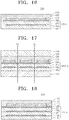
- FIG. 16 is a cross-sectional view illustrating an organic light-emitting display apparatus 200 according to an exemplary embodiment of the present invention.
- the organic light-emitting display apparatus 200 includes a flexible substrate FS-3, a TFT layer 110, an organic light-emitting device layer 120, and a thin film encapsulating layer 130.
- a flexible substrate FS-3 a TFT layer 110
- an organic light-emitting device layer 120 a thin film encapsulating layer 130.
- a thin film encapsulating layer 130 a thin film encapsulating layer 130.
- a flexible substrate FS-3 of the organic light-emitting display apparatus 200 includes a first plastic layer 1PL, a first barrier layer 1BL, a second plastic layer 2PL, and a second barrier layer 2BL.
- the first barrier layer 1BL and the second barrier layer 2BL are patterned to be disposed in an area where the organic light-emitting device layer 120 is formed in this embodiment.
- the second barrier layer 2BL is patterned to have a larger area than the first barrier layer 1BL.
- the first barrier layer 1BL is formed to overlap with the organic light-emitting device layer 120 without extending beyond the organic light-emitting device layer 120, while the second barrier layer 2BL is formed to overlap with the organic light-emitting device layer 120 while extending beyond the organic light-emitting device layer 120 by an extension amount.
- the extension amount of the second barrier layer 2BL is only a relatively small amount (e.g. not formed across the whole of the non-display area between the unit display devices 200).
- FIG. 17 is a cross-sectional view illustrating a process of manufacturing an organic light-emitting display apparatus 200 according to an exemplary embodiment of the present invention.
- FIG. 17 is a cross-sectional view illustrating a process of forming a mother flexible substrate MFS-3 on a glass substrate GS.
- a first barrier layer 1BL which is patterned
- a second plastic layer 2PL which is patterned
- a second barrier layer 2BL which is patterned
- the first barrier layer 1BL and the second barrier layer 2BL are formed only in an area corresponding to each unit display device 200, and are not formed in a non-display area between the unit display devices 200. Accordingly, during a process of dividing a plurality of organic light-emitting device layers on the mother flexible substrate MFS-3 into a plurality of unit display devices 200, an inorganic layer such as the first barrier layer 1BL and the second barrier layer 2BL is formed smaller along a cutting line CL, so that cracks or pollutants due to the inorganic layer may be reduced during a cutting process.
- first barrier layer 1BL and the second barrier layer 2BL are not formed at an end part of the glass substrate GS, an area where the first barrier layer 1BL and the second plastic layer 2PL overlap is not formed at an end part of the glass substrate GS.
- an end part of the second plastic layer 2PL and an end part of the first plastic layer 1PL are in direct contact at an end part of the glass substrate GS.
- an area of the second barrier layer 2BL is larger than that of the first barrier layer 1BL as shown in FIGS. 16 and 17 , the present invention is not limited thereto.
- the area of the second barrier layer 2BL may be equal to or less than that of the first barrier layer 1BL.
- FIG. 18 is a cross-sectional view illustrating an organic light-emitting display apparatus 300 according to an exemplary embodiment of the present invention.
- the organic light-emitting display apparatus 300 includes a flexible substrate FS-4, a TFT layer 110, an organic light-emitting device layer 120, and a thin film encapsulating layer 130.
- a difference from the organic light-emitting display apparatus 100 described above will be mainly described.
- Like reference numerals may refer to like elements.
- a flexible substrate FS-4 of the organic light-emitting display apparatus 300 may include a first plastic layer 1PL, a first barrier layer 1BL, a second plastic layer 2PL, a second barrier layer 2BL, a third plastic layer 3PL, and a third barrier layer 3BL.
- the flexible substrate FS-3 includes three alternately-stacked plastic layers and three barrier layers, an average water and vapor transmission path becomes longer compared to the organic light-emitting display apparatus 100 discussed above, so that the transmission of oxygen and moisture may be further prevented.
- first barrier layer 1BL and the second plastic layer 2PL are patterned, the delamination between the first barrier layer 1BL and the second plastic layer 2PL and between the second barrier layer 2BL and the third plastic layer 3PL may be prevented.
- the first barrier layer 1BL and the second barrier layer 2BL are formed to overlap with the organic light-emitting device layer 120 without extending beyond the organic light-emitting device layer 120, while the third barrier layer 3BL is formed to extend beyond the organic light-emitting device layer 120.
- FIG. 18 Although a structure including alternately-stacked three plastic layers and three barrier layers is shown in FIG. 18 , a plastic layer and a barrier layer may be further stacked where desired.
- the present invention may also be applied to various flexible display devices in addition to an organic light-emitting display apparatus.
- the present invention may be applied to various electronic devices such as a portable mobile device, a navigation system, a video camera, a notebook PC, a tablet PC, a flat screen TV, and a beam projector.
- a flexible substrate since a flexible substrate includes two plastic layers and two barrier layers which are alternately stacked, an average vapor transmission path becomes longer, thereby preventing the deterioration of an OLED.
- the two plastic layers are in direct contact in a region where the barrier layer is patterned, so that the delamination between the barrier layer and the two plastic layers may be prevented.
- an organic light-emitting display apparatus comprising: a first flexible plastic layer; a first barrier layer formed over the first flexible plastic layer, the first barrier layer being substantially impervious to water and oxygen; a second flexible plastic layer formed over the first barrier layer; an organic light-emitting device layer formed over the second flexible plastic layer; and a thin film encapsulating layer encapsulating the organic light-emitting device layer, wherein the first barrier layer is patterned to correspond to an area where the organic light-emitting device layer is formed.
- the first barrier layer is patterned as an island shape.
- the first barrier layer is patterned to have the same or substantially the same area as the organic light-emitting device layer.
- the second barrier layer is patterned to be located in an area where the organic light-emitting device layer is formed. In some such embodiments, the second barrier layer can have a greater area than the first barrier layer. In some such embodiments, the second barrier layer is in contact with the thin film encapsulating layer in an outer part of an area where the organic light-emitting device layer is formed.
- Some embodiments provide a method of manufacturing an organic light-emitting display apparatus, the method comprising: preparing a carrier substrate; forming a mother flexible substrate over the carrier substrate, the mother flexible substrate including a first plastic layer, a first barrier layer, substantially impervious to water and oxygen, patterned to have a plurality of an island shapes, and a second plastic layer, which are sequentially stacked; forming a plurality of organic light-emitting device layers each at a position respectively corresponding to an area where a said island first barrier layer is patterned on the mother flexible substrate; forming a thin film encapsulating layer encapsulating the plurality of organic light-emitting device layers; and separating the carrier substrate from the mother flexible substrate.
Landscapes
- Engineering & Computer Science (AREA)
- Manufacturing & Machinery (AREA)
- Physics & Mathematics (AREA)
- Optics & Photonics (AREA)
- Chemical & Material Sciences (AREA)
- Inorganic Chemistry (AREA)
- Microelectronics & Electronic Packaging (AREA)
- Electroluminescent Light Sources (AREA)
Claims (11)
- Organische lichtemittierende Anzeigevorrichtung (100), umfassend:eine erste flexible Kunststoffschicht (1 PL);eine erste Sperrschicht (1BL), die gänzlich in direktem Kontakt mit der ersten flexiblen Kunststoffschicht (1 PL) steht,wobei die erste Sperrschicht (1 BL) im Wesentlichen wasser- und sauerstoffundurchlässig ist;eine zweite flexible Kunststoffschicht (2PL), die über der ersten Sperrschicht (1 BL) ausgebildet ist;eine organische lichtemittierende Einrichtungsschicht (120), die über der zweiten flexiblen Kunststoffschicht (2PL) ausgebildet ist;eine Dünnfilmverkapselungsschicht (130), die die organische lichtemittierende Einrichtungsschicht (120) verkapselt; undeine zweite Sperrschicht (2BL) zwischen der zweiten flexiblen Kunststoffschicht (2PL) und der organischen lichtemittierenden Einrichtungsschicht (120), wobei die zweite Sperrschicht (2BL) im Wesentlichen wasser- und sauerstoffundurchlässig ist, wobei die erste Sperrschicht (1 BL) gemustert ist um einem Bereich zu entsprechen, in dem die organische lichtemittierende Einrichtungsschicht (120) ausgebildet ist, ohne sich über die organische lichtemittierende Einrichtungsschicht (120) hinaus zu erstrecken,wobei die erste flexible Kunststoffschicht (1 PL) in einem Bereich, der die erste Sperrschicht (1BL) umgibt, in direktem Kontakt mit der zweiten flexiblen Kunststoffschicht (2PL) steht; undwobei die zweite Sperrschicht (2BL) nicht in Kontakt mit der ersten flexiblen Kunststoffschicht (1 PL) steht, und wobei die zweite Sperrschicht (2BL) ausgebildet ist, um sich über die organische lichtemittierende Einrichtungsschicht (120) hinaus zu erstrecken, um mit der Dünnfilmverkapselungsschicht (130) in einem äußeren Teil eines Bereiches, in dem die organische lichtemittierende Einrichtungsschicht (120) ausgebildet ist, in Kontakt zu stehen.
- Organische lichtemittierende Anzeigevorrichtung nach Anspruch 1, wobei die zweite Sperrschicht mindestens eine Schicht umfasst, die ein anorganisches Material enthält.
- Organische lichtemittierende Anzeigevorrichtung nach Anspruch 1 oder 2, wobei mindestens ein Paar von Schichten zwischen der zweiten Sperrschicht und der organischen lichtemittierenden Einrichtungsschicht ausgebildet ist, wobei jedes Paar von Schichten eine dritte flexible Kunststoffschicht und eine dritte Sperrschicht, die im Wesentlichen wasser- und sauerstoffundurchlässig sind, enthält;
wobei gegebenenfalls die zweite Sperrschicht gemustert ist, um sich in einem Bereich zu befinden, in dem die organische lichtemittierende Einrichtungsschicht ausgebildet ist. - Organische lichtemittierende Anzeigevorrichtung nach einem der Ansprüche 1 bis 3, wobei die erste flexible Kunststoffschicht und die zweite flexible Kunststoffschicht Polymid, Polyethylennaphthalat, Polyethylenterephthalat, Polyarylat, Polycarbonat, Polyethersulfon oder Polyetherimid umfassen.
- Organische lichtemittierende Anzeigevorrichtung nach einem der Ansprüche 1 bis 4, wobei eine Dicke der zweiten flexiblen Kunststoffschicht größer ist als die der ersten flexiblen Kunststoffschicht; und/oderwobei die zweite flexible Kunststoffschicht eine niedrigere Viskosität aufweist als die erste flexible Kunststoffschicht; und/oderwobei die erste Sperrschicht und/oder die zweite Sperrschicht mindestens eine Schicht umfasst, die ein anorganisches Material enthält.
- Elektronische Einrichtung, die die organische lichtemittierende Anzeigevorrichtung nach einem der Ansprüche 1 bis 5 enthält.
- Verfahren zur Herstellung einer organischen lichtemittierenden Anzeigevorrichtung (100), das Verfahren umfassend:Vorbereiten eines Trägersubstrates (GS);Ausbilden eines flexiblen Muttersubstrates über dem Trägersubstrat (GS),wobei das flexible Muttersubstrat eine erste Kunststoffschicht (1 PL), eine erste Sperrschicht (1BL), die im Wesentlichen wasser- und sauerstoffundurchlässig ist und gemustert ist, um eine Mehrzahl von Inselformen aufzuweisen, und eine zweite Kunststoffschicht (2PL), die abwechselnd geschichtet sind, enthält;Ausbilden einer Mehrzahl organischer lichtemittierender Einrichtungsschichten (120) jeweils an einer Stelle, die einem entsprechenden Bereich entspricht, in dem eine der Inseln der ersten Sperrschicht (1BL) auf dem flexiblen Muttersubstrat gemustert ist,wobei jede Insel der ersten Sperrschicht (1 BL) mit der entsprechenden organischen lichtemittierenden Einrichtungsschicht (120) überlappt, ohne sich über die jeweilige organische lichtemittierende Einrichtungsschicht (120) hinaus zu erstrecken;Ausbilden einer Dünnfilmverkapselungsschicht (130), die die Mehrzahl organischer lichtemittierender Einrichtungsschichten (120) verkapselt; undTrennen des Trägersubstrates (GS) von dem flexiblen Muttersubstrat, wobei die erste flexible Kunststoffschicht (1 PL) in einem Bereich, der die erste Sperrschicht (1 BL) umgibt, in Kontakt mit der zweiten flexiblen Kunststoffschicht (2PL) steht; wobei das Ausbilden des flexiblen Muttersubstrates ferner das Ausbilden einer zweiten Sperrschicht (2BL), die im Wesentlichen wasser- und sauerstoffundurchlässig ist, zwischen der zweiten Kunststoffschicht (2PL) und den organischen lichtemittierenden Einrichtungsschichten (120) umfasst, wobei die zweite Sperrschicht (2BL) nicht in Kontakt mit der ersten flexiblen Kunststoffschicht (1 PL) steht,wobei die zweite Sperrschicht (2BL) dazu ausgebildet ist, sich unter den organischen lichtemittierenden Einrichtungsschichten (120) zu erstrecken, um in einem äußeren Teil eines Bereiches, in dem jede organische lichtemittierende Einrichtungsschicht (120) ausgebildet ist, in Kontakt mit der Dünnfilmverkapselungsschicht (130) zu stehen.
- Verfahren nach Anspruch 7, wobei das Trennen des Trägersubstrates von dem flexiblen Muttersubstrat das Ausstrahlen eines Laserstrahls von einer entgegengesetzten Richtung einer Seite, auf der das flexible Muttersubstrat des Trägersubstrates ausgebildet ist, umfasst, um das Trägersubstrat von dem flexiblen Muttersubstrat zu Trennen;
wobei gegebenenfalls der Laserstrahl ein ultraviolettes (UV) Licht ist. - Verfahren nach Anspruch 7 oder 8, wobei das Ausbilden des flexiblen Muttersubstrates ferner das Ausbilden mindestens eines Paares von Strukturen zwischen der zweiten Sperrschicht und den organischen lichtemittierenden Einrichtungsschichten umfasst, wobei jede Struktur eine dritte Kunststoffschicht und eine dritte Sperrschicht, die im Wesentlichen wasser- und sauerstoffundurchlässig ist, enthält.
- Verfahren nach einem der Ansprüche 7 bis 9, wobei das Ausbilden des flexiblen Muttersubstrates das Ausbilden der zweiten Kunststoffschicht umfasst, um einen Bereich aufzuweisen, der gleich groß oder kleiner als der der ersten Kunststoffschicht ist;
wobei gegebenenfalls ein Endteil der zweiten Kunststoffschicht und ein Endteil der ersten Kunststoffschicht an einem Endteil des Trägersubstrates in direktem Kontakt stehen. - Verfahren nach einem der Ansprüche 7 bis 10, wobei das Ausbilden des flexiblen Muttersubstrates das Ausbilden der zweiten Kunststoffschicht umfasst, um eine geringere Viskosität als die erste Kunststoffschicht aufzuweisen; und/oderwobei das Ausbilden des flexiblen Muttersubstrates das Ausbilden der zweiten Kunststoffschicht, sodass sie dicker als die erste Kunststoffschicht ist, umfasst; und/oderwobei das Trägersubstrat ein Glassubstrat ist; und/oderferner umfassend das Aufteilen der organischen lichtemittierenden Einrichtungsschichten auf dem flexiblen Muttersubstrat in eine Mehrzahl von Einheitsanzeigevorrichtungen nach der Trennung des Trägersubstrates von dem flexiblen Muttersubstrat.
Applications Claiming Priority (1)
| Application Number | Priority Date | Filing Date | Title |
|---|---|---|---|
| KR1020130059260A KR102133433B1 (ko) | 2013-05-24 | 2013-05-24 | 유기 발광 표시 장치, 이를 포함하는 전자 기기, 및 유기 발광 표시 장치의 제조 방법 |
Publications (2)
| Publication Number | Publication Date |
|---|---|
| EP2806473A1 EP2806473A1 (de) | 2014-11-26 |
| EP2806473B1 true EP2806473B1 (de) | 2020-05-06 |
Family
ID=50721700
Family Applications (1)
| Application Number | Title | Priority Date | Filing Date |
|---|---|---|---|
| EP14168669.1A Active EP2806473B1 (de) | 2013-05-24 | 2014-05-16 | Organische lichtemittierende Anzeigevorrichtung mit einem flexiblen Substrat |
Country Status (5)
| Country | Link |
|---|---|
| US (1) | US9406905B2 (de) |
| EP (1) | EP2806473B1 (de) |
| KR (1) | KR102133433B1 (de) |
| CN (2) | CN107958924B (de) |
| TW (1) | TWI645593B (de) |
Families Citing this family (63)
| Publication number | Priority date | Publication date | Assignee | Title |
|---|---|---|---|---|
| CN104377165B (zh) * | 2013-08-12 | 2017-11-17 | 上海和辉光电有限公司 | 平板显示器及其柔性基板和制作方法 |
| GB2519081B (en) * | 2013-10-08 | 2019-07-03 | Flexenable Ltd | Electronic devices including organic materials |
| CN103682177B (zh) * | 2013-12-16 | 2015-03-25 | 深圳市华星光电技术有限公司 | 柔性oled面板的制作方法 |
| US20160181574A1 (en) * | 2014-01-03 | 2016-06-23 | Shenzhen China Star Optoelectronics Technology Co., Ltd. | Method for manufacturing flexible oled (organic light emitting diode) panel |
| KR102369298B1 (ko) * | 2014-04-29 | 2022-03-03 | 삼성디스플레이 주식회사 | 플렉서블 디스플레이 장치 및 그 제조방법 |
| GB2527872B (en) | 2014-06-30 | 2018-01-10 | Lg Display Co Ltd | Display device |
| CN110459665A (zh) * | 2014-12-26 | 2019-11-15 | Ns材料株式会社 | 波长转换构件的制造方法 |
| CN104795424B (zh) | 2015-03-26 | 2017-11-10 | 京东方科技集团股份有限公司 | 柔性衬底基板和显示基板及其制作方法、显示装置 |
| WO2016168341A1 (en) * | 2015-04-13 | 2016-10-20 | Royole Corporation | Support and detachment of flexible substrates |
| CN105118837A (zh) * | 2015-09-16 | 2015-12-02 | 京东方科技集团股份有限公司 | 一种柔性基底及其制备方法、显示装置 |
| US10395594B1 (en) * | 2015-09-18 | 2019-08-27 | Apple Inc. | Hybrid microdriver and TFT architecture |
| US10395590B1 (en) | 2015-09-18 | 2019-08-27 | Apple Inc. | Hybrid microdriver architecture for driving microLED displays |
| US10395589B1 (en) | 2015-09-18 | 2019-08-27 | Apple Inc. | Hybrid microdriver architectures having relaxed comparator requirements |
| CN105244366B (zh) * | 2015-11-23 | 2018-03-30 | 武汉华星光电技术有限公司 | 柔性显示基板及其制造方法 |
| CN105552247B (zh) * | 2015-12-08 | 2018-10-26 | 上海天马微电子有限公司 | 复合基板、柔性显示装置及其制备方法 |
| CN105374952A (zh) * | 2015-12-15 | 2016-03-02 | 信利半导体有限公司 | 一种oled器件的制造方法及oled器件和应用 |
| KR102513210B1 (ko) * | 2015-12-31 | 2023-03-22 | 엘지디스플레이 주식회사 | 플렉서블 표시장치 및 그의 제조방법 |
| KR102567547B1 (ko) | 2016-03-22 | 2023-08-17 | 삼성디스플레이 주식회사 | 디스플레이 장치 |
| JP6863803B2 (ja) | 2016-04-07 | 2021-04-21 | 株式会社半導体エネルギー研究所 | 表示装置 |
| US10741590B2 (en) | 2016-04-12 | 2020-08-11 | Semiconductor Energy Laboratory Co., Ltd. | Peeling method and manufacturing method of flexible device |
| US10181424B2 (en) | 2016-04-12 | 2019-01-15 | Semiconductor Energy Laboratory Co., Ltd. | Peeling method and manufacturing method of flexible device |
| US10003023B2 (en) | 2016-04-15 | 2018-06-19 | Semiconductor Energy Laboratory Co., Ltd. | Display device and electronic device |
| WO2017182909A1 (en) * | 2016-04-22 | 2017-10-26 | Semiconductor Energy Laboratory Co., Ltd. | Separation method and manufacturing method of flexible device |
| CN107546330A (zh) * | 2016-06-29 | 2018-01-05 | 张家港市鸿嘉数字科技有限公司 | 一种柔性oled衬底 |
| CN107546332A (zh) * | 2016-06-29 | 2018-01-05 | 张家港市鸿嘉数字科技有限公司 | 一种柔性oled封装方法 |
| KR102513204B1 (ko) | 2016-08-17 | 2023-03-22 | 가부시키가이샤 한도오따이 에네루기 켄큐쇼 | 표시 장치 |
| KR102608416B1 (ko) | 2016-09-06 | 2023-12-01 | 삼성디스플레이 주식회사 | 디스플레이 장치 |
| US11374184B2 (en) | 2016-09-08 | 2022-06-28 | Boe Technology Group Co., Ltd. | Flexible substrate and fabrication method thereof, and flexible display apparatus |
| CN106206945A (zh) | 2016-09-08 | 2016-12-07 | 京东方科技集团股份有限公司 | 一种柔性基板及其制备方法、柔性显示装置 |
| CN106328683B (zh) * | 2016-10-11 | 2019-04-30 | 武汉华星光电技术有限公司 | 柔性oled显示器及其制作方法 |
| KR102712661B1 (ko) * | 2016-10-17 | 2024-10-04 | 삼성디스플레이 주식회사 | 디스플레이 장치 |
| CN108153440B (zh) * | 2016-12-06 | 2021-01-26 | 和鑫光电股份有限公司 | 软性可挠触摸显示屏及其制造方法 |
| CN106585069A (zh) * | 2016-12-23 | 2017-04-26 | 武汉华星光电技术有限公司 | 柔性基板、面板及丝网印刷机制作柔性基板、面板的方法 |
| CN106601776A (zh) * | 2016-12-26 | 2017-04-26 | 武汉华星光电技术有限公司 | 柔性amoled显示面板 |
| CN106843389B (zh) * | 2017-01-09 | 2022-08-05 | Oppo广东移动通信有限公司 | 电子装置 |
| US10170600B2 (en) | 2017-01-12 | 2019-01-01 | Semiconductor Energy Laboratory Co., Ltd. | Method for manufacturing semiconductor device |
| US10510993B1 (en) | 2017-02-27 | 2019-12-17 | Sharp Kabushiki Kaisha | Production method for EL device |
| CN107195643B (zh) * | 2017-07-12 | 2020-11-03 | 武汉天马微电子有限公司 | 柔性显示面板及其制作方法、柔性显示装置 |
| KR102083315B1 (ko) | 2017-09-11 | 2020-03-03 | 삼성디스플레이 주식회사 | 유기 발광 표시 장치 및 이의 제조 방법 |
| CN107732025A (zh) * | 2017-09-25 | 2018-02-23 | 上海九山电子科技有限公司 | 一种有机发光显示面板及有机发光显示装置 |
| WO2019073567A1 (ja) * | 2017-10-12 | 2019-04-18 | シャープ株式会社 | ベース層を備えた非可撓性基板、可撓性表示装置及びその製造方法 |
| KR102471464B1 (ko) * | 2017-10-31 | 2022-11-25 | 엘지디스플레이 주식회사 | 디스플레이 장치 |
| CN107993918A (zh) * | 2017-11-09 | 2018-05-04 | 信利半导体有限公司 | 一种柔性显示器的制备方法 |
| KR102523976B1 (ko) | 2017-11-21 | 2023-04-20 | 삼성전자주식회사 | 디스플레이 장치 |
| JP2019124811A (ja) * | 2018-01-16 | 2019-07-25 | 株式会社ジャパンディスプレイ | 表示装置及び表示装置の製造方法 |
| KR102522591B1 (ko) | 2018-02-05 | 2023-04-17 | 삼성디스플레이 주식회사 | 표시 장치 및 이의 제조 방법 |
| CN108630732B (zh) * | 2018-04-25 | 2020-07-28 | 深圳市华星光电技术有限公司 | Oled显示面板及其制作方法 |
| CN108666421A (zh) * | 2018-05-23 | 2018-10-16 | 京东方科技集团股份有限公司 | 柔性基底、有机电致发光二极管显示基板和显示装置 |
| KR102675480B1 (ko) | 2018-06-15 | 2024-06-13 | 삼성디스플레이 주식회사 | 표시 장치 |
| KR102547989B1 (ko) * | 2018-07-25 | 2023-06-23 | 엘지디스플레이 주식회사 | 유기 발광 소자를 이용한 조명 장치 및 이의 제조 방법 |
| KR102480881B1 (ko) * | 2018-07-25 | 2022-12-22 | 엘지디스플레이 주식회사 | 유기 발광 소자를 이용한 조명 장치 및 이의 제조 방법 |
| KR102465374B1 (ko) | 2018-09-12 | 2022-11-10 | 삼성디스플레이 주식회사 | 표시 패널 및 이를 포함하는 표시 장치 |
| KR102612769B1 (ko) | 2018-11-09 | 2023-12-11 | 엘지디스플레이 주식회사 | 표시장치 및 이의 제조방법 |
| KR102857938B1 (ko) * | 2018-12-13 | 2025-09-09 | 엘지디스플레이 주식회사 | 플렉서블 유기발광표시장치 |
| CN109671758A (zh) * | 2018-12-18 | 2019-04-23 | 武汉华星光电半导体显示技术有限公司 | 显示面板及其制备方法、显示装置 |
| KR102134794B1 (ko) * | 2018-12-26 | 2020-07-17 | 박홍진 | 유기발광소자의 제조방법 |
| KR102713879B1 (ko) * | 2019-04-29 | 2024-10-04 | 엘지디스플레이 주식회사 | 플렉서블 표시장치 |
| KR20210019633A (ko) * | 2019-08-12 | 2021-02-23 | 삼성디스플레이 주식회사 | 표시 장치 및 표시 장치의 제조 방법 |
| CN110534646A (zh) * | 2019-08-21 | 2019-12-03 | 合肥维信诺科技有限公司 | 柔性基板及其制备方法、显示装置 |
| CN110649183A (zh) | 2019-09-02 | 2020-01-03 | 武汉华星光电半导体显示技术有限公司 | 一种显示面板的制作方法 |
| CN110729335B (zh) * | 2019-10-28 | 2022-02-01 | 武汉华星光电半导体显示技术有限公司 | 显示面板及其制备方法 |
| KR102830303B1 (ko) * | 2019-12-30 | 2025-07-03 | 엘지디스플레이 주식회사 | 유기 발광 표시 장치 및 이의 제조 방법 |
| US12433109B2 (en) | 2021-04-28 | 2025-09-30 | Chengdu Boe Optoelectronics Technology Co., Ltd. | Display substrate, preparation method thereof, and display apparatus |
Citations (2)
| Publication number | Priority date | Publication date | Assignee | Title |
|---|---|---|---|---|
| KR20110133881A (ko) * | 2010-06-07 | 2011-12-14 | 동아대학교 산학협력단 | 표시 장치용 플렉서블 기판 및 그의 제조 방법 |
| US20120223350A1 (en) * | 2011-03-04 | 2012-09-06 | Semiconductor Energy Laboratory Co., Ltd. | Light-Emitting Device, Lighting Device, Substrate, and Manufacturing Method of Substrate |
Family Cites Families (19)
| Publication number | Priority date | Publication date | Assignee | Title |
|---|---|---|---|---|
| US5811177A (en) * | 1995-11-30 | 1998-09-22 | Motorola, Inc. | Passivation of electroluminescent organic devices |
| US7198832B2 (en) | 1999-10-25 | 2007-04-03 | Vitex Systems, Inc. | Method for edge sealing barrier films |
| US6664137B2 (en) * | 2001-03-29 | 2003-12-16 | Universal Display Corporation | Methods and structures for reducing lateral diffusion through cooperative barrier layers |
| JP5127103B2 (ja) | 2001-09-10 | 2013-01-23 | 株式会社半導体エネルギー研究所 | 発光装置及び電子機器 |
| JP2005123012A (ja) | 2003-10-16 | 2005-05-12 | Pioneer Electronic Corp | 有機エレクトロルミネセンス表示パネルとその製造方法 |
| GB0327093D0 (en) | 2003-11-21 | 2003-12-24 | Koninkl Philips Electronics Nv | Active matrix displays and other electronic devices having plastic substrates |
| JP2005317476A (ja) * | 2004-04-30 | 2005-11-10 | Toshiba Matsushita Display Technology Co Ltd | 表示装置 |
| KR100759691B1 (ko) * | 2006-07-04 | 2007-09-17 | 삼성에스디아이 주식회사 | 평판 표시 장치의 제조 방법 |
| KR20080073942A (ko) | 2007-02-07 | 2008-08-12 | 엘지전자 주식회사 | 플렉서블 디스플레이 장치 및 그 제조 방법 |
| JP5296343B2 (ja) * | 2007-07-31 | 2013-09-25 | 住友化学株式会社 | バリア層つき基板、表示素子および表示素子の製造方法 |
| EP2091096A1 (de) * | 2008-02-15 | 2009-08-19 | Nederlandse Organisatie voor toegepast-natuurwetenschappelijk Onderzoek TNO | Verkapselte elektronische Vorrichtung und Herstellungsverfahren |
| JP5345831B2 (ja) * | 2008-12-16 | 2013-11-20 | 富士ゼロックス株式会社 | 電子写真感光体、プロセスカートリッジ、及び画像形成装置 |
| KR101001552B1 (ko) * | 2009-01-20 | 2010-12-17 | 삼성모바일디스플레이주식회사 | 유기 발광 표시 장치 |
| KR101155907B1 (ko) * | 2009-06-04 | 2012-06-20 | 삼성모바일디스플레이주식회사 | 유기 발광 표시 장치 및 그 제조 방법 |
| KR101148144B1 (ko) | 2009-09-07 | 2012-05-23 | 고려대학교 산학협력단 | 플렉시블 가스 배리어 필름, 그 제조방법 및 이를 이용한 플렉시블 디스플레이 소자 |
| KR101108161B1 (ko) | 2009-12-24 | 2012-01-31 | 삼성모바일디스플레이주식회사 | 유기 발광 표시 장치 및 그 제조방법 |
| KR101746677B1 (ko) * | 2010-11-02 | 2017-06-13 | 엘지디스플레이 주식회사 | 플렉서블 유기전계발광소자 |
| KR101757736B1 (ko) | 2010-12-31 | 2017-07-14 | 엘지디스플레이 주식회사 | 유기전계 발광소자 제조용 증착장치 및 이를 이용한 증착 방법 |
| TWI552883B (zh) * | 2011-07-25 | 2016-10-11 | Lintec Corp | Gas barrier film laminates and electronic components |
-
2013
- 2013-05-24 KR KR1020130059260A patent/KR102133433B1/ko active Active
-
2014
- 2014-03-14 US US14/213,678 patent/US9406905B2/en active Active
- 2014-05-15 TW TW103117108A patent/TWI645593B/zh active
- 2014-05-16 EP EP14168669.1A patent/EP2806473B1/de active Active
- 2014-05-21 CN CN201810004632.3A patent/CN107958924B/zh active Active
- 2014-05-21 CN CN201410216151.0A patent/CN104183783B/zh active Active
Patent Citations (2)
| Publication number | Priority date | Publication date | Assignee | Title |
|---|---|---|---|---|
| KR20110133881A (ko) * | 2010-06-07 | 2011-12-14 | 동아대학교 산학협력단 | 표시 장치용 플렉서블 기판 및 그의 제조 방법 |
| US20120223350A1 (en) * | 2011-03-04 | 2012-09-06 | Semiconductor Energy Laboratory Co., Ltd. | Light-Emitting Device, Lighting Device, Substrate, and Manufacturing Method of Substrate |
Also Published As
| Publication number | Publication date |
|---|---|
| TW201445793A (zh) | 2014-12-01 |
| US9406905B2 (en) | 2016-08-02 |
| CN107958924B (zh) | 2022-04-29 |
| US20140346473A1 (en) | 2014-11-27 |
| CN107958924A (zh) | 2018-04-24 |
| CN104183783A (zh) | 2014-12-03 |
| KR102133433B1 (ko) | 2020-07-14 |
| KR20140137950A (ko) | 2014-12-03 |
| TWI645593B (zh) | 2018-12-21 |
| CN104183783B (zh) | 2018-02-02 |
| EP2806473A1 (de) | 2014-11-26 |
Similar Documents
| Publication | Publication Date | Title |
|---|---|---|
| EP2806473B1 (de) | Organische lichtemittierende Anzeigevorrichtung mit einem flexiblen Substrat | |
| KR102104608B1 (ko) | 유기 발광 표시 장치, 이를 포함하는 전자 기기, 및 유기 발광 표시 장치의 제조 방법 | |
| TWI688089B (zh) | 有機發光二極體顯示器、包含該有機發光二極體顯示器之電子裝置、及製造該有機發光二極體顯示器之方法 | |
| TWI581420B (zh) | 有機發光顯示設備及其製造方法 | |
| KR102092707B1 (ko) | 플렉서블 디스플레이 장치와, 이의 제조 방법 | |
| US20140339527A1 (en) | Organic light-emitting diode display, an electronic device including the same, and method of manufacturing the organic light-emitting diode display | |
| KR20140140983A (ko) | 유기 발광 표시 장치 및 이의 제조 방법 | |
| KR20140075467A (ko) | 디스플레이 장치 및 디스플레이 장치의 제조방법 | |
| KR102696809B1 (ko) | 유기 발광 표시 장치, 이를 포함하는 전자 기기, 및 유기 발광 표시 장치의 제조 방법 | |
| KR102184678B1 (ko) | 유기 발광 표시 장치, 이를 포함하는 전자 기기, 및 유기 발광 표시 장치의 제조 방법 |
Legal Events
| Date | Code | Title | Description |
|---|---|---|---|
| PUAI | Public reference made under article 153(3) epc to a published international application that has entered the european phase |
Free format text: ORIGINAL CODE: 0009012 |
|
| 17P | Request for examination filed |
Effective date: 20140516 |
|
| AK | Designated contracting states |
Kind code of ref document: A1 Designated state(s): AL AT BE BG CH CY CZ DE DK EE ES FI FR GB GR HR HU IE IS IT LI LT LU LV MC MK MT NL NO PL PT RO RS SE SI SK SM TR |
|
| AX | Request for extension of the european patent |
Extension state: BA ME |
|
| R17P | Request for examination filed (corrected) |
Effective date: 20150526 |
|
| RBV | Designated contracting states (corrected) |
Designated state(s): AL AT BE BG CH CY CZ DE DK EE ES FI FR GB GR HR HU IE IS IT LI LT LU LV MC MK MT NL NO PL PT RO RS SE SI SK SM TR |
|
| RAP1 | Party data changed (applicant data changed or rights of an application transferred) |
Owner name: SAMSUNG DISPLAY CO., LTD. |
|
| STAA | Information on the status of an ep patent application or granted ep patent |
Free format text: STATUS: EXAMINATION IS IN PROGRESS |
|
| 17Q | First examination report despatched |
Effective date: 20170228 |
|
| REG | Reference to a national code |
Ref country code: DE Ref legal event code: R079 Ref document number: 602014064834 Country of ref document: DE Free format text: PREVIOUS MAIN CLASS: H01L0051000000 Ipc: H01L0051520000 |
|
| GRAP | Despatch of communication of intention to grant a patent |
Free format text: ORIGINAL CODE: EPIDOSNIGR1 |
|
| STAA | Information on the status of an ep patent application or granted ep patent |
Free format text: STATUS: GRANT OF PATENT IS INTENDED |
|
| RIC1 | Information provided on ipc code assigned before grant |
Ipc: H01L 27/32 20060101ALI20191028BHEP Ipc: H01L 51/52 20060101AFI20191028BHEP Ipc: H01L 51/00 20060101ALI20191028BHEP Ipc: H01L 51/56 20060101ALI20191028BHEP |
|
| INTG | Intention to grant announced |
Effective date: 20191118 |
|
| GRAS | Grant fee paid |
Free format text: ORIGINAL CODE: EPIDOSNIGR3 |
|
| GRAA | (expected) grant |
Free format text: ORIGINAL CODE: 0009210 |
|
| STAA | Information on the status of an ep patent application or granted ep patent |
Free format text: STATUS: THE PATENT HAS BEEN GRANTED |
|
| AK | Designated contracting states |
Kind code of ref document: B1 Designated state(s): AL AT BE BG CH CY CZ DE DK EE ES FI FR GB GR HR HU IE IS IT LI LT LU LV MC MK MT NL NO PL PT RO RS SE SI SK SM TR |
|
| REG | Reference to a national code |
Ref country code: GB Ref legal event code: FG4D |
|
| REG | Reference to a national code |
Ref country code: CH Ref legal event code: EP Ref country code: AT Ref legal event code: REF Ref document number: 1268261 Country of ref document: AT Kind code of ref document: T Effective date: 20200515 |
|
| REG | Reference to a national code |
Ref country code: IE Ref legal event code: FG4D |
|
| REG | Reference to a national code |
Ref country code: DE Ref legal event code: R096 Ref document number: 602014064834 Country of ref document: DE |
|
| REG | Reference to a national code |
Ref country code: LT Ref legal event code: MG4D |
|
| REG | Reference to a national code |
Ref country code: NL Ref legal event code: MP Effective date: 20200506 |
|
| PG25 | Lapsed in a contracting state [announced via postgrant information from national office to epo] |
Ref country code: FI Free format text: LAPSE BECAUSE OF FAILURE TO SUBMIT A TRANSLATION OF THE DESCRIPTION OR TO PAY THE FEE WITHIN THE PRESCRIBED TIME-LIMIT Effective date: 20200506 Ref country code: LT Free format text: LAPSE BECAUSE OF FAILURE TO SUBMIT A TRANSLATION OF THE DESCRIPTION OR TO PAY THE FEE WITHIN THE PRESCRIBED TIME-LIMIT Effective date: 20200506 Ref country code: IS Free format text: LAPSE BECAUSE OF FAILURE TO SUBMIT A TRANSLATION OF THE DESCRIPTION OR TO PAY THE FEE WITHIN THE PRESCRIBED TIME-LIMIT Effective date: 20200906 Ref country code: SE Free format text: LAPSE BECAUSE OF FAILURE TO SUBMIT A TRANSLATION OF THE DESCRIPTION OR TO PAY THE FEE WITHIN THE PRESCRIBED TIME-LIMIT Effective date: 20200506 Ref country code: GR Free format text: LAPSE BECAUSE OF FAILURE TO SUBMIT A TRANSLATION OF THE DESCRIPTION OR TO PAY THE FEE WITHIN THE PRESCRIBED TIME-LIMIT Effective date: 20200807 Ref country code: NO Free format text: LAPSE BECAUSE OF FAILURE TO SUBMIT A TRANSLATION OF THE DESCRIPTION OR TO PAY THE FEE WITHIN THE PRESCRIBED TIME-LIMIT Effective date: 20200806 Ref country code: PT Free format text: LAPSE BECAUSE OF FAILURE TO SUBMIT A TRANSLATION OF THE DESCRIPTION OR TO PAY THE FEE WITHIN THE PRESCRIBED TIME-LIMIT Effective date: 20200907 |
|
| PG25 | Lapsed in a contracting state [announced via postgrant information from national office to epo] |
Ref country code: HR Free format text: LAPSE BECAUSE OF FAILURE TO SUBMIT A TRANSLATION OF THE DESCRIPTION OR TO PAY THE FEE WITHIN THE PRESCRIBED TIME-LIMIT Effective date: 20200506 Ref country code: RS Free format text: LAPSE BECAUSE OF FAILURE TO SUBMIT A TRANSLATION OF THE DESCRIPTION OR TO PAY THE FEE WITHIN THE PRESCRIBED TIME-LIMIT Effective date: 20200506 Ref country code: LV Free format text: LAPSE BECAUSE OF FAILURE TO SUBMIT A TRANSLATION OF THE DESCRIPTION OR TO PAY THE FEE WITHIN THE PRESCRIBED TIME-LIMIT Effective date: 20200506 Ref country code: BG Free format text: LAPSE BECAUSE OF FAILURE TO SUBMIT A TRANSLATION OF THE DESCRIPTION OR TO PAY THE FEE WITHIN THE PRESCRIBED TIME-LIMIT Effective date: 20200806 |
|
| REG | Reference to a national code |
Ref country code: AT Ref legal event code: MK05 Ref document number: 1268261 Country of ref document: AT Kind code of ref document: T Effective date: 20200506 |
|
| PG25 | Lapsed in a contracting state [announced via postgrant information from national office to epo] |
Ref country code: NL Free format text: LAPSE BECAUSE OF FAILURE TO SUBMIT A TRANSLATION OF THE DESCRIPTION OR TO PAY THE FEE WITHIN THE PRESCRIBED TIME-LIMIT Effective date: 20200506 Ref country code: AL Free format text: LAPSE BECAUSE OF FAILURE TO SUBMIT A TRANSLATION OF THE DESCRIPTION OR TO PAY THE FEE WITHIN THE PRESCRIBED TIME-LIMIT Effective date: 20200506 |
|
| PG25 | Lapsed in a contracting state [announced via postgrant information from national office to epo] |
Ref country code: ES Free format text: LAPSE BECAUSE OF FAILURE TO SUBMIT A TRANSLATION OF THE DESCRIPTION OR TO PAY THE FEE WITHIN THE PRESCRIBED TIME-LIMIT Effective date: 20200506 Ref country code: SM Free format text: LAPSE BECAUSE OF FAILURE TO SUBMIT A TRANSLATION OF THE DESCRIPTION OR TO PAY THE FEE WITHIN THE PRESCRIBED TIME-LIMIT Effective date: 20200506 Ref country code: LI Free format text: LAPSE BECAUSE OF NON-PAYMENT OF DUE FEES Effective date: 20200531 Ref country code: EE Free format text: LAPSE BECAUSE OF FAILURE TO SUBMIT A TRANSLATION OF THE DESCRIPTION OR TO PAY THE FEE WITHIN THE PRESCRIBED TIME-LIMIT Effective date: 20200506 Ref country code: DK Free format text: LAPSE BECAUSE OF FAILURE TO SUBMIT A TRANSLATION OF THE DESCRIPTION OR TO PAY THE FEE WITHIN THE PRESCRIBED TIME-LIMIT Effective date: 20200506 Ref country code: RO Free format text: LAPSE BECAUSE OF FAILURE TO SUBMIT A TRANSLATION OF THE DESCRIPTION OR TO PAY THE FEE WITHIN THE PRESCRIBED TIME-LIMIT Effective date: 20200506 Ref country code: IT Free format text: LAPSE BECAUSE OF FAILURE TO SUBMIT A TRANSLATION OF THE DESCRIPTION OR TO PAY THE FEE WITHIN THE PRESCRIBED TIME-LIMIT Effective date: 20200506 Ref country code: AT Free format text: LAPSE BECAUSE OF FAILURE TO SUBMIT A TRANSLATION OF THE DESCRIPTION OR TO PAY THE FEE WITHIN THE PRESCRIBED TIME-LIMIT Effective date: 20200506 Ref country code: CZ Free format text: LAPSE BECAUSE OF FAILURE TO SUBMIT A TRANSLATION OF THE DESCRIPTION OR TO PAY THE FEE WITHIN THE PRESCRIBED TIME-LIMIT Effective date: 20200506 Ref country code: CH Free format text: LAPSE BECAUSE OF NON-PAYMENT OF DUE FEES Effective date: 20200531 |
|
| REG | Reference to a national code |
Ref country code: DE Ref legal event code: R097 Ref document number: 602014064834 Country of ref document: DE |
|
| PG25 | Lapsed in a contracting state [announced via postgrant information from national office to epo] |
Ref country code: PL Free format text: LAPSE BECAUSE OF FAILURE TO SUBMIT A TRANSLATION OF THE DESCRIPTION OR TO PAY THE FEE WITHIN THE PRESCRIBED TIME-LIMIT Effective date: 20200506 Ref country code: MC Free format text: LAPSE BECAUSE OF FAILURE TO SUBMIT A TRANSLATION OF THE DESCRIPTION OR TO PAY THE FEE WITHIN THE PRESCRIBED TIME-LIMIT Effective date: 20200506 Ref country code: SK Free format text: LAPSE BECAUSE OF FAILURE TO SUBMIT A TRANSLATION OF THE DESCRIPTION OR TO PAY THE FEE WITHIN THE PRESCRIBED TIME-LIMIT Effective date: 20200506 |
|
| PLBE | No opposition filed within time limit |
Free format text: ORIGINAL CODE: 0009261 |
|
| STAA | Information on the status of an ep patent application or granted ep patent |
Free format text: STATUS: NO OPPOSITION FILED WITHIN TIME LIMIT |
|
| REG | Reference to a national code |
Ref country code: BE Ref legal event code: MM Effective date: 20200531 |
|
| PG25 | Lapsed in a contracting state [announced via postgrant information from national office to epo] |
Ref country code: LU Free format text: LAPSE BECAUSE OF NON-PAYMENT OF DUE FEES Effective date: 20200516 |
|
| 26N | No opposition filed |
Effective date: 20210209 |
|
| PG25 | Lapsed in a contracting state [announced via postgrant information from national office to epo] |
Ref country code: IE Free format text: LAPSE BECAUSE OF NON-PAYMENT OF DUE FEES Effective date: 20200516 |
|
| PG25 | Lapsed in a contracting state [announced via postgrant information from national office to epo] |
Ref country code: BE Free format text: LAPSE BECAUSE OF NON-PAYMENT OF DUE FEES Effective date: 20200531 Ref country code: SI Free format text: LAPSE BECAUSE OF FAILURE TO SUBMIT A TRANSLATION OF THE DESCRIPTION OR TO PAY THE FEE WITHIN THE PRESCRIBED TIME-LIMIT Effective date: 20200506 |
|
| PG25 | Lapsed in a contracting state [announced via postgrant information from national office to epo] |
Ref country code: TR Free format text: LAPSE BECAUSE OF FAILURE TO SUBMIT A TRANSLATION OF THE DESCRIPTION OR TO PAY THE FEE WITHIN THE PRESCRIBED TIME-LIMIT Effective date: 20200506 Ref country code: MT Free format text: LAPSE BECAUSE OF FAILURE TO SUBMIT A TRANSLATION OF THE DESCRIPTION OR TO PAY THE FEE WITHIN THE PRESCRIBED TIME-LIMIT Effective date: 20200506 Ref country code: CY Free format text: LAPSE BECAUSE OF FAILURE TO SUBMIT A TRANSLATION OF THE DESCRIPTION OR TO PAY THE FEE WITHIN THE PRESCRIBED TIME-LIMIT Effective date: 20200506 |
|
| PG25 | Lapsed in a contracting state [announced via postgrant information from national office to epo] |
Ref country code: MK Free format text: LAPSE BECAUSE OF FAILURE TO SUBMIT A TRANSLATION OF THE DESCRIPTION OR TO PAY THE FEE WITHIN THE PRESCRIBED TIME-LIMIT Effective date: 20200506 |
|
| REG | Reference to a national code |
Ref country code: DE Ref legal event code: R079 Ref document number: 602014064834 Country of ref document: DE Free format text: PREVIOUS MAIN CLASS: H01L0051520000 Ipc: H10K0050800000 |
|
| P01 | Opt-out of the competence of the unified patent court (upc) registered |
Effective date: 20230515 |
|
| PGFP | Annual fee paid to national office [announced via postgrant information from national office to epo] |
Ref country code: DE Payment date: 20250422 Year of fee payment: 12 |
|
| PGFP | Annual fee paid to national office [announced via postgrant information from national office to epo] |
Ref country code: FR Payment date: 20250422 Year of fee payment: 12 |
|
| PGFP | Annual fee paid to national office [announced via postgrant information from national office to epo] |
Ref country code: GB Payment date: 20260324 Year of fee payment: 13 |