EP2805156B1 - System und herstellungsverfahren für das system mit einer sensoranordnung und einer microwell-struktur auf der sensoranordnung - Google Patents
System und herstellungsverfahren für das system mit einer sensoranordnung und einer microwell-struktur auf der sensoranordnung Download PDFInfo
- Publication number
- EP2805156B1 EP2805156B1 EP13704258.6A EP13704258A EP2805156B1 EP 2805156 B1 EP2805156 B1 EP 2805156B1 EP 13704258 A EP13704258 A EP 13704258A EP 2805156 B1 EP2805156 B1 EP 2805156B1
- Authority
- EP
- European Patent Office
- Prior art keywords
- layer
- well
- sensor
- over
- forming
- Prior art date
- Legal status (The legal status is an assumption and is not a legal conclusion. Google has not performed a legal analysis and makes no representation as to the accuracy of the status listed.)
- Active
Links
Images






Classifications
-
- G—PHYSICS
- G01—MEASURING; TESTING
- G01N—INVESTIGATING OR ANALYSING MATERIALS BY DETERMINING THEIR CHEMICAL OR PHYSICAL PROPERTIES
- G01N27/00—Investigating or analysing materials by the use of electric, electrochemical, or magnetic means
- G01N27/26—Investigating or analysing materials by the use of electric, electrochemical, or magnetic means by investigating electrochemical variables; by using electrolysis or electrophoresis
- G01N27/403—Cells and electrode assemblies
- G01N27/414—Ion-sensitive or chemical field-effect transistors, i.e. ISFETS or CHEMFETS
- G01N27/4148—Integrated circuits therefor, e.g. fabricated by CMOS processing
-
- G—PHYSICS
- G01—MEASURING; TESTING
- G01N—INVESTIGATING OR ANALYSING MATERIALS BY DETERMINING THEIR CHEMICAL OR PHYSICAL PROPERTIES
- G01N27/00—Investigating or analysing materials by the use of electric, electrochemical, or magnetic means
- G01N27/26—Investigating or analysing materials by the use of electric, electrochemical, or magnetic means by investigating electrochemical variables; by using electrolysis or electrophoresis
- G01N27/27—Association of two or more measuring systems or cells, each measuring a different parameter, where the measurement results may be either used independently, the systems or cells being physically associated, or combined to produce a value for a further parameter
-
- B—PERFORMING OPERATIONS; TRANSPORTING
- B01—PHYSICAL OR CHEMICAL PROCESSES OR APPARATUS IN GENERAL
- B01L—CHEMICAL OR PHYSICAL LABORATORY APPARATUS FOR GENERAL USE
- B01L3/00—Containers or dishes for laboratory use, e.g. laboratory glassware; Droppers
- B01L3/50—Containers for the purpose of retaining a material to be analysed, e.g. test tubes
- B01L3/502—Containers for the purpose of retaining a material to be analysed, e.g. test tubes with fluid transport, e.g. in multi-compartment structures
- B01L3/5027—Containers for the purpose of retaining a material to be analysed, e.g. test tubes with fluid transport, e.g. in multi-compartment structures by integrated microfluidic structures, i.e. dimensions of channels and chambers are such that surface tension forces are important, e.g. lab-on-a-chip
-
- G—PHYSICS
- G01—MEASURING; TESTING
- G01N—INVESTIGATING OR ANALYSING MATERIALS BY DETERMINING THEIR CHEMICAL OR PHYSICAL PROPERTIES
- G01N27/00—Investigating or analysing materials by the use of electric, electrochemical, or magnetic means
- G01N27/26—Investigating or analysing materials by the use of electric, electrochemical, or magnetic means by investigating electrochemical variables; by using electrolysis or electrophoresis
- G01N27/403—Cells and electrode assemblies
- G01N27/414—Ion-sensitive or chemical field-effect transistors, i.e. ISFETS or CHEMFETS
- G01N27/4145—Ion-sensitive or chemical field-effect transistors, i.e. ISFETS or CHEMFETS specially adapted for biomolecules, e.g. gate electrode with immobilised receptors
-
- H—ELECTRICITY
- H10—SEMICONDUCTOR DEVICES; ELECTRIC SOLID-STATE DEVICES NOT OTHERWISE PROVIDED FOR
- H10P—GENERIC PROCESSES OR APPARATUS FOR THE MANUFACTURE OR TREATMENT OF DEVICES COVERED BY CLASS H10
- H10P14/00—Formation of materials, e.g. in the shape of layers or pillars
- H10P14/60—Formation of materials, e.g. in the shape of layers or pillars of insulating materials
-
- H—ELECTRICITY
- H10—SEMICONDUCTOR DEVICES; ELECTRIC SOLID-STATE DEVICES NOT OTHERWISE PROVIDED FOR
- H10P—GENERIC PROCESSES OR APPARATUS FOR THE MANUFACTURE OR TREATMENT OF DEVICES COVERED BY CLASS H10
- H10P50/00—Etching of wafers, substrates or parts of devices
-
- B—PERFORMING OPERATIONS; TRANSPORTING
- B01—PHYSICAL OR CHEMICAL PROCESSES OR APPARATUS IN GENERAL
- B01L—CHEMICAL OR PHYSICAL LABORATORY APPARATUS FOR GENERAL USE
- B01L2200/00—Solutions for specific problems relating to chemical or physical laboratory apparatus
- B01L2200/06—Fluid handling related problems
- B01L2200/0647—Handling flowable solids, e.g. microscopic beads, cells, particles
- B01L2200/0668—Trapping microscopic beads
-
- B—PERFORMING OPERATIONS; TRANSPORTING
- B01—PHYSICAL OR CHEMICAL PROCESSES OR APPARATUS IN GENERAL
- B01L—CHEMICAL OR PHYSICAL LABORATORY APPARATUS FOR GENERAL USE
- B01L2200/00—Solutions for specific problems relating to chemical or physical laboratory apparatus
- B01L2200/12—Specific details about manufacturing devices
-
- B—PERFORMING OPERATIONS; TRANSPORTING
- B01—PHYSICAL OR CHEMICAL PROCESSES OR APPARATUS IN GENERAL
- B01L—CHEMICAL OR PHYSICAL LABORATORY APPARATUS FOR GENERAL USE
- B01L2300/00—Additional constructional details
- B01L2300/06—Auxiliary integrated devices, integrated components
- B01L2300/0627—Sensor or part of a sensor is integrated
- B01L2300/0636—Integrated biosensor, microarrays
-
- B—PERFORMING OPERATIONS; TRANSPORTING
- B01—PHYSICAL OR CHEMICAL PROCESSES OR APPARATUS IN GENERAL
- B01L—CHEMICAL OR PHYSICAL LABORATORY APPARATUS FOR GENERAL USE
- B01L2300/00—Additional constructional details
- B01L2300/06—Auxiliary integrated devices, integrated components
- B01L2300/0627—Sensor or part of a sensor is integrated
- B01L2300/0645—Electrodes
-
- B—PERFORMING OPERATIONS; TRANSPORTING
- B01—PHYSICAL OR CHEMICAL PROCESSES OR APPARATUS IN GENERAL
- B01L—CHEMICAL OR PHYSICAL LABORATORY APPARATUS FOR GENERAL USE
- B01L2300/00—Additional constructional details
- B01L2300/08—Geometry, shape and general structure
- B01L2300/0809—Geometry, shape and general structure rectangular shaped
- B01L2300/0819—Microarrays; Biochips
-
- B—PERFORMING OPERATIONS; TRANSPORTING
- B01—PHYSICAL OR CHEMICAL PROCESSES OR APPARATUS IN GENERAL
- B01L—CHEMICAL OR PHYSICAL LABORATORY APPARATUS FOR GENERAL USE
- B01L2300/00—Additional constructional details
- B01L2300/08—Geometry, shape and general structure
- B01L2300/0861—Configuration of multiple channels and/or chambers in a single devices
- B01L2300/0877—Flow chambers
-
- B—PERFORMING OPERATIONS; TRANSPORTING
- B01—PHYSICAL OR CHEMICAL PROCESSES OR APPARATUS IN GENERAL
- B01L—CHEMICAL OR PHYSICAL LABORATORY APPARATUS FOR GENERAL USE
- B01L2300/00—Additional constructional details
- B01L2300/08—Geometry, shape and general structure
- B01L2300/0893—Geometry, shape and general structure having a very large number of wells, microfabricated wells
-
- G—PHYSICS
- G01—MEASURING; TESTING
- G01N—INVESTIGATING OR ANALYSING MATERIALS BY DETERMINING THEIR CHEMICAL OR PHYSICAL PROPERTIES
- G01N27/00—Investigating or analysing materials by the use of electric, electrochemical, or magnetic means
- G01N27/26—Investigating or analysing materials by the use of electric, electrochemical, or magnetic means by investigating electrochemical variables; by using electrolysis or electrophoresis
-
- Y—GENERAL TAGGING OF NEW TECHNOLOGICAL DEVELOPMENTS; GENERAL TAGGING OF CROSS-SECTIONAL TECHNOLOGIES SPANNING OVER SEVERAL SECTIONS OF THE IPC; TECHNICAL SUBJECTS COVERED BY FORMER USPC CROSS-REFERENCE ART COLLECTIONS [XRACs] AND DIGESTS
- Y10—TECHNICAL SUBJECTS COVERED BY FORMER USPC
- Y10T—TECHNICAL SUBJECTS COVERED BY FORMER US CLASSIFICATION
- Y10T436/00—Chemistry: analytical and immunological testing
- Y10T436/14—Heterocyclic carbon compound [i.e., O, S, N, Se, Te, as only ring hetero atom]
-
- Y—GENERAL TAGGING OF NEW TECHNOLOGICAL DEVELOPMENTS; GENERAL TAGGING OF CROSS-SECTIONAL TECHNOLOGIES SPANNING OVER SEVERAL SECTIONS OF THE IPC; TECHNICAL SUBJECTS COVERED BY FORMER USPC CROSS-REFERENCE ART COLLECTIONS [XRACs] AND DIGESTS
- Y10—TECHNICAL SUBJECTS COVERED BY FORMER USPC
- Y10T—TECHNICAL SUBJECTS COVERED BY FORMER US CLASSIFICATION
- Y10T436/00—Chemistry: analytical and immunological testing
- Y10T436/14—Heterocyclic carbon compound [i.e., O, S, N, Se, Te, as only ring hetero atom]
- Y10T436/142222—Hetero-O [e.g., ascorbic acid, etc.]
-
- Y—GENERAL TAGGING OF NEW TECHNOLOGICAL DEVELOPMENTS; GENERAL TAGGING OF CROSS-SECTIONAL TECHNOLOGIES SPANNING OVER SEVERAL SECTIONS OF THE IPC; TECHNICAL SUBJECTS COVERED BY FORMER USPC CROSS-REFERENCE ART COLLECTIONS [XRACs] AND DIGESTS
- Y10—TECHNICAL SUBJECTS COVERED BY FORMER USPC
- Y10T—TECHNICAL SUBJECTS COVERED BY FORMER US CLASSIFICATION
- Y10T436/00—Chemistry: analytical and immunological testing
- Y10T436/14—Heterocyclic carbon compound [i.e., O, S, N, Se, Te, as only ring hetero atom]
- Y10T436/142222—Hetero-O [e.g., ascorbic acid, etc.]
- Y10T436/143333—Saccharide [e.g., DNA, etc.]
Definitions
- This disclosure in general, relates to sensor arrays and methods for making same.
- Electronic sensor arrays are finding increased use for detecting analytes in fluids, such as gases or liquids.
- arrays of sensors based on field effect transistors are finding use in detecting ionic components, such as various cations, anions or pH.
- Such sensors are often referred to as ion-sensitive field effect transistors or ISFETs.
- nucleotide addition results in the release of ionic species that influence the pH in a local environment.
- Sensors of the sensor arrays are used to detect changes in pH in the local environment resulting from the nucleotide addition.
- the pH of the local environment can be influenced by adjacent environments, referred to as crosstalk, and can be influenced by the interaction of various materials with hydrogen ions, leading to lower accuracy and less sensitivity to the changes caused by nucleotide addition.
- US2010/300895 discloses an array of electronic sensors integrated with a microwell array for confining analytes and/or particles for analytical reactions and a method for identifying microwells containing analytes and/or particles by passing a sensor-active reagent over the array and correlating sensor response times to the presence or absence of analytes or particles.
- US 2010/052080 describes a biosensor chip for detecting biological particles, the biosensor chip comprising a sensor active region being sensitive for the biological particles and being arranged in a Back End of the Line portion of the biosensor chip.
- US 2010/137143 describes methods and an apparatus relating to FET arrays including large FET arrays for monitoring chemical and/or biological reactions such as nucleic acid sequencing-by-synthesis reactions.
- US2012/045368 describes a method of fabricating a chemical detection device, the method comprising forming a microwell above a CMOS device, the microwell comprising a bottom surface and sidewalls.
- the method may further comprise applying a first chemical to be selectively attached to the bottom surface of the microwell, forming a metal oxide layer on the sidewalls of the microwell, and applying a second chemical to be selectively attached to the sidewalls of the microwell.
- the second chemical may lack an affinity to the first chemical.
- a system in an aspect in accordance with the teachings of the present disclosure, includes a sensor including a sensor pad and a well wall structure defining a well operatively connected to the sensor pad.
- the sensor pad is associated with a lower surface of the well.
- the well wall structure defines an upper surface and a wall surface extending between the upper surface and the lower surface.
- the upper surface is defined by an upper buffer material having an intrinsic buffer capacity of at least 2 ⁇ l017 groups/m2.
- the wall surface is defined by a wall material having an intrinsic buffer capacity of not greater than 1.7 ⁇ l017 groups/m2.
- a method of forming a sensor system includes forming a structural layer over a sensor device.
- the sensor device includes a sensor pad.
- the structural layer includes a structural material having an intrinsic buffer capacity of not greater than 1.7 ⁇ l0 17 groups/m2.
- the method further includes forming a buffer layer over the structural layer.
- the buffer layer includes a buffer material having an intrinsic buffer capacity of at least 2 ⁇ l0 17 groups/m2.
- the method also includes etching the buffer layer and the structural layer to define a well operatively connected to the sensor pad.
- a method of sequencing a polynucleotide includes applying a particle comprising a plurality of copies of a polynucleotide to a well of a system of the first aspect, exposing the particle to an aqueous solution including a nucleotide, and measuring a response of the device to the exposing.
- a system in an aspect in accordance with the teachings of the present disclosure, includes a sensor device including a sensor pad and a well wall structure defining a well in operative connection with the sensor pad. A lower surface of the well is defined over the sensor pad.
- the well wall structure has an upper surface and a wall surface extending between the upper surface and the lower surface.
- the system includes a passivation film disposed over the upper surface, the wall surface and the lower surface and an isolation film disposed over the passivation film opposite the well wall structure and extending substantially parallel to and at least along a portion of the wall surface.
- the passivation layer is exposed at least along a portion of the upper surface and at least along a portion of the lower surface.
- a method of forming a sensor system includes forming a structural layer over a sensor device, the sensor device including a sensor pad and etching the structural layer to define a well operatively connected to the sensor pad. A lower surface of the well is defined over the sensor pad.
- the structurally layer has an upper surface and a wall surface extending between the upper surface and the lower surface.
- the method includes forming a passivation film over the structural layer. The passivation film extends along at least a portion of the upper surface and extends over the wall surface and the lower surface.
- the method further includes forming an isolation film over the passivation film and etching the isolation film to expose the passivation film along at least the portion of the upper surface and at least a portion of the lower surface.
- a method of sequencing a polynucleotide includes applying a particle comprising a plurality of copies of a polynucleotide to a well of a system of the fourth aspect, exposing the particle to an aqueous solution including a nucleotide, and measuring a response of the device to the exposing.
- a system in an example not forming part of the invention, includes a sensor device including a sensor pad and a well wall structure defining a well in operative connection with the sensor pad.
- a lower surface of the well is defined over the sensor pad.
- the well wall structure has an upper surface, and a wall surface extends between the upper surface and the lower surface.
- a metal layer is disposed over the well wall structure and extends along the upper surface and the wall surface.
- a method of forming a sensor system includes forming a structural layer over a sensor device, the sensor device including a sensor pad, and etching the structural layer to form a trench defining a well post over the senor pad and a well wall structure opposite the first structure, the well post extending vertically higher than the well wall structure.
- the method further includes depositing a metal layer into the trench and over the well post and the well wall structure, exposing the well post, and etching to remove the well post.
- a method of forming a sensor system includes forming a structural layer over a sensor device, the sensor device including a sensor pad, etching the structural layer to form a well post over the senor pad, depositing a metal layer to surround the well post, and etching to remove the well post.
- a method of sequencing a polynucleotide includes applying a particle comprising a plurality of copies of a polynucleotide to a well of a system of the seventh aspect, exposing the particle to an aqueous solution including a nucleotide, and measuring a response of the device to the exposing.
- the invention is defined by a sensor system according to claim 1.
- a sensor system according to claim 1.
- such a system can reduce the influence of an adjacent well on the local environment of the well and can improve sensitivity of the sensor.
- a sequencing system includes a flow cell in which a sensory array is disposed, includes communication circuitry in electronic communication with the sensory array, and includes containers and fluid controls in fluidic communication with the flow cell.
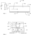
- FIG. 1 illustrates an expanded and cross-sectional view of a flow cell 100 and illustrates a portion of a flow chamber 106.
- a reagent flow 108 flows across a surface of a microwell array 102, in which the reagent flow 108 flows over the open ends of microwells of the microwell array 102.
- the microwell array 102 and a sensor array 105 together may form an integrated unit forming a lower wall (or floor) of flow cell 100.
- a reference electrode 104 may be fluidly coupled to flow chamber 106.
- a flow cell cover 130 encapsulates flow chamber 106 to contain reagent flow 108 within a confined region.
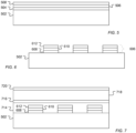
- FIG. 2 illustrates an expanded view of a microwell 201 and a sensor 214, as illustrated at 110 of FIG. 1 .
- the volume, shape, aspect ratio (such as base width-to-well depth ratio), and other dimensional characteristics of the microwells may be selected based on the nature of the reaction taking place, as well as the reagents, byproducts, or labeling techniques (if any) that are employed.
- the sensor 214 can be a chemical field-effect transistor (chemFET), more specifically an ion-sensitive FET (ISFET), with a floating gate 218 having a sensor plate 220 separated from the microwell interior by a passivation layer 216.
- chemFET chemical field-effect transistor
- ISFET ion-sensitive FET
- the sensor 214 can be responsive to (and generate an output signal related to) the amount of a charge 224 present on passivation layer 216 opposite the sensor plate 220. Changes in the charge 224 can cause changes in a current between a source 221 and a drain 222 of the chemFET. In turn, the chemFET can be used directly to provide a current-based output signal or indirectly with additional circuitry to provide a voltage-based output signal. Reactants, wash solutions, and other reagents may move in and out of the microwells by a diffusion mechanism 240.
- Reactions carried out in the microwell 201 can be analytical reactions to identify or determine characteristics or properties of an analyte of interest. Such reactions can generate directly or indirectly byproducts that affect the amount of charge adjacent to the sensor plate 220. If such byproducts are produced in small amounts or rapidly decay or react with other constituents, then multiple copies of the same analyte may be analyzed in the microwell 201 at the same time in order to increase the output signal generated. In an embodiment, multiple copies of an analyte may be attached to a solid phase support 212, either before or after deposition into the microwell 201.
- the solid phase support 212 may be microparticles, nanoparticles, beads, solid or porous comprising gels, or the like.
- solid phase support 212 is also referred herein as a particle.
- multiple, connected copies may be made by rolling circle amplification (RCA), exponential RCA, or like techniques, to produce an amplicon without the need of a solid support.
- RCA rolling circle amplification
- exponential RCA exponential RCA
- FIG. 3 illustrates a system 300 including a well wall structure 302 defining wells 304.
- the wells 304 are in operative connection with sensor pads 306 of sensors.
- a lower surface 308 of the well 304 is defined over at least a portion of the sensor pad 306.
- the well wall structure 302 defines an upper surface 310 and defines a wall surface 312 extending between the upper surface 310 and the lower surface 308.
- the well wall structure 302 can be formed of one or more layers of material.
- the well wall structure 302 can have a thickness extending from the lower surface 308 to the upper surface 310 in a range of 0.3 micrometers to 10 micrometers, such as a range of 0.5 micrometers to 6 micrometers.
- the wells 304 can have a characteristic diameter, defined as the square root of 4 times the cross-sectional area (A) divided by Pi (e.g., sqrt(4*A/ ⁇ ), of not greater than 5 micrometers, such as not greater than 3.5 micrometers, not greater than 2.0 micrometers, not greater than 1.6 micrometers, not greater than 1.0 micrometers, not greater than 0.8 micrometers or even not greater than 0.6 micrometers.
- the upper surface 310 is defined by an upper buffer material having an intrinsic buffer capacity of at least 2xl0 17 groups/m 2 .
- Intrinsic buffer capacity is defined as the surface density of hydroxyl groups on a surface of a material measured at a pH of 7.
- a buffer material is referred to as a high intrinsic buffer capacity material.
- the upper buffer material can have an intrinsic buffer capacity of at least 4 ⁇ 10 17 groups/m 2 , such as at least 8 ⁇ 10 17 groups/m 2 , at least 1 ⁇ 10 18 groups/m 2 , or even at least 2 ⁇ 10 18 groups/m 2 .
- the upper buffer material has an intrinsic buffer capacity of not greater than 1 ⁇ 10 21 groups/m 2 .
- the upper buffer material is a high intrinsic buffer capacity material that can include an inorganic material, such as a ceramic material.
- a ceramic material can include an oxide of aluminum, hafnium, tantalum, zirconium, or any combination thereof.
- the ceramic material can include an oxide of tantalum.
- the ceramic material includes an oxide of zirconium.
- the upper surface 310 can be coated with a pH buffering coating.
- An exemplary pH buffering coating can include a functional group, such as phosphate, phosphonate, catechol, nitrocatechol, boronate, phenylboronate, imidazole, silanol, another pH-sensing group, or a combination thereof.
- the wall surface 312 is defined by a wall material having a low intrinsic buffer capacity, such as not greater than 1.7 ⁇ 10 17 groups/m 2 .
- the intrinsic buffer capacity of the wall material can be not greater than 1 ⁇ 10 17 groups/m 2 , such as not greater than 5 ⁇ 10 16 groups/m 2 , not greater than 2 ⁇ 10 16 groups/m 2 , not greater than 1 ⁇ 10 16 groups/m 2 , or even not greater than 5 ⁇ 10 15 groups/m 2 .
- the wall material includes a low intrinsic buffer capacity material that can include an inorganic material, such as a ceramic material.
- An exemplary ceramic material can include a nitride of silica, titanium, or a combination thereof.
- the ceramic material includes an oxide of silicon.
- the ceramic material can include silicon oxynitride.
- the inorganic material can include a metal.
- the metal can include aluminum, copper, nickel, titanium, silver, gold, platinum, or a combination thereof.
- the metal can include copper.
- the wall material can include an organic material, such as a polymeric material.
- An exemplary polymeric material includes a polymer having an aromatic group in its backbone.
- the polymer can be a poly(xylylene), such as a poly(p-xylylene), optionally including functionalize p-xylylenes, such as halogenated p-xylylenes.
- the polymeric material includes a fluoropolymer.
- An exemplary fluoropolymer includes polytetrafluoroethylene (PTFE), polyvinylidene fluoride (PVDF), polyvinyl fluoride (PVF), fluorinated ethylene propylene (FEP) copolymer, ethylene chlorotrifluoroethylene (ECTFE) copolymer, a copolymer of tetrafluoroethylene, hexafluoropropylene, and vinylidene fluoride (THV), a copolymer of tetrafluoroethylene and perfluoro methylvinylether (PFA or MFA), a fluoropolymer having a fluorinated oxolane in its backbone, perfluoroether, or any combination thereof.
- PTFE polytetrafluoroethylene
- PVDF polyvinylidene fluoride
- PVF polyvinyl fluoride
- FEP fluorinated ethylene propylene copolymer
- ECTFE ethylene chloro
- the fluoropolymer can be a fluoropolymer having fluorinated oxolane in its backbone, for example, Cytop.
- the polymer coating can be amorphous, exhibiting little or no crystallinity.
- the wall material can include a low buffer capacity coating.
- the low buffer capacity coating can include a silane component.
- organofunctional groups R can include methyl, methylene, phenyl, benzyl, anilino, amino, amide, hydroxyl, aldehyde, alkoxy, halo, mercapto, carboxy, acyl, vinyl, allyl, styryl, epoxy, isocyanato, glycidoxy, acryloxy, or a combination thereof.
- silane component can include N-((6-aminohexyl)aminomethyltriethoxysilane, (mercaptomethyl)methyldiethoxysilane, chloromethyltriethoxysilane, (isocyanatomethyl)methyldimethoxysilane, N-phenylaminomethyltriethoxysilane, triethoxysilylundecanal, 11-mercaptoundecyltrimethoxysilane, 10-undecenyltrimethoxysilane, N-(2-aminoethyl)-11-aminoundecyltrimethoxysilane, 11-bromoundecyltrimethoxysilane, n-octyltrimethoxysilane, 2-[methoxy(polyethyleneoxy)propyl]trimethoxysilane, 3-methoxypropyltrimethoxysilane, methoxytriethyleneoxypropyltrisilane, methoxyprop
- the lower surface 308 of the well can be defined by lower buffer material disposed over the sensor pad 306.
- the lower buffer material can have an intrinsic buffer capacity of at least 2xl0 17 groups/m 2 , such as at least 4x10 17 groups/m 2 , at least 8 ⁇ 10 17 groups/m 2 , at least 1 ⁇ 10 18 groups/m 2 , or even at least 2 ⁇ 10 18 groups/m 2 .
- the lower buffer material has an intrinsic buffer capacity of not greater than 1 ⁇ 10 21 groups/m 2 .
- the lower buffer material can include an inorganic material, such as a ceramic material.
- a ceramic material can include an oxide of aluminum, hafnium, tantalum, zirconium, or any combination thereof.
- the ceramic material can include an oxide of tantalum.
- the ceramic material includes an oxide of zirconium.
- the lower surface 308 can be coated with a pH sensitive coating.
- Exemplary pH sensitive coatings can include a functional group, such as phosphate, phosphonate, catechol, nitrocatechol, boronate, phenylboronate, imidazole, silanol, another pH-sensing group, or a combination thereof.
- the lower buffer material can be the same as the upper buffer material.
- the lower buffer material and the upper buffer material can be formed as a single layer over the well wall structure 302.
- the upper buffer material and lower buffer material can be formed as separate layers and can be different.
- the wall surface 312 extends substantially vertically, defined as extending in a direction having a component that is normal to the surface defined by the sensor pad.
- a well wall 402 can extend vertically, being parallel to a normal component 412 of a surface 414 defined by a sensor pad.
- the wall surface 404 extends substantially vertically, in an outward direction away from the sensor pad, providing a larger opening to the well than the area of the lower surface of the well. As illustrated in FIG. 4 , the wall surface 404 extends in a direction having a vertical component parallel to the normal component 412 of the surface 414.
- a wall surface 406 extends substantially vertically in an inward direction, providing an opening area that is smaller than an area of the lower surface of the well.
- the wall surface 406 extends in a direction having a component parallel to the normal component 412 of the surface 414.
- surfaces 402, 404, or 406 are illustrated by straight lines, some semiconductor or CMOS manufacturing processes can result in structures having nonlinear shapes.
- wall surfaces such as wall surface 408 and upper surfaces, such as upper surface 410, can be arcuate in shape or take various nonlinear forms.
- structures and devices illustrated herewith are depicted as having linear layers, surfaces, or shapes, actual layers, surfaces, or shapes resulting from semiconductor processing may differ to some degree, possibly including nonlinear and arcuate variations of the illustrated embodiment.
- the well wall structure 302 and the surfaces 310, 312, and 308 can be defined by one or more materials. Specific embodiments are presented below that identify specific material layers. However, it is understood that various materials described above can be substituted for the identified material layers.
- a well wall structure includes one or more layers defining the well wall. Such layers can be formed of materials having low intrinsic buffer capacity.
- the well wall structure includes a film defining an upper surface of the well wall structure, which is formed of a buffer material having a high intrinsic buffer capacity.
- a lower surface of the well is defined by a passivation material having high buffer capacity.
- the passivation material is disposed over a sensor pad.
- FIG. 9 includes an illustration of an exemplary well wall structure 828 that defines a well 822 over a passivation layer 610 and a sensor pad 608. The passivation layer 610 is exposed to form a lower surface 930 of the well 822.
- the well wall structure 828 defines a wall surface 824 extending between an upper surface 826 and the lower surface 930.
- the well wall structure 828 includes one or more layers of low intrinsic buffer capacity material that define the wall surface 824.
- An additional film 720 defines the upper surface 826 and is formed of a high intrinsic buffer capacity material.
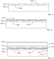
- a structure such as that illustrated in FIG. 9 can be formed by a process such as a process illustrated in FIGs. 5-9 .
- a conductive layer 504 is deposited over a CMOS structure 502.
- the CMOS structure 502 can include a sensor structure to be operatively coupled to a sensory pad.
- one or more passivation layers 506 or 508 can be deposited over the conductive layer 504.
- the conductive layer 504 is formed by a metal deposition technique, such as atomic layer deposition, sputtering, e-beam evaporation, electrochemical deposition, or a combination thereof.
- the passivation layers 506 or 508 can be deposited over the conductive layer 504 using atomic layer deposition or other techniques.
- the passivation layers 506 or 508 can include an oxide of aluminum, hafnium, tantalum, zirconium, or a combination thereof.
- the passivation layer 506 includes an oxide of tantalum and the passivation layer 508 includes an oxide of aluminum.
- the layers 504, 506, or 508 can be patterned to expose a surface of the CMOS structure 502 and define stack structures 606.
- a stack structure 606 including a conductive sensor pad 608 can overlie the CMOS structure 502.
- a layer 610 includes tantalum oxide and a layer 612 includes aluminum oxide.
- an aluminum oxide layer (not illustrated) can be disposed between the sensor pad 608 and the layer 610.
- the layers 610 or 612 can be formed of zirconium oxide.
- each of the layers 610 or 612 can have a thickness in a range of 5 nm to 100 nm, such as a range of 10 nm to 70 nm, a range of 15 nm to 65 nm, or even a range of 20 nm to 50 nm.
- one or more layers 714, 716, or 718 can be deposited over the CMOS structure 502 and the sensor pad 608.
- one or more layers of an oxide of silicon, a nitride of silicon, or TEOS can be deposited to overlie the stack structure 606.
- a layer 714 of silicon oxide is deposited over the CMOS structure 502.
- a layer 716 of silicon nitride is deposited over the layer 714
- a layer 718 of silicon oxide or TEOS is deposited over the layer 714.
- a buffer material layer 720 can be deposited over the layers 714, 716 or 718.
- the total thickness of the one or more layers 714, 716, 718, or 720 can be in a range of 0.3 micrometers to 10 micrometers, such as a range of 0.5 micrometers to 6 micrometers.
- the layers 714, 716, 718, or 720 can be etched to define a well 822 and a well wall structure 828.
- the wells 822 can be exposed using a wet patch, a plasma etch, or a combination thereof.
- a fluorinated plasma etch process with endpoint detection can be utilized to form a well that terminates at the aluminum oxide layer 612.
- a fluorinated plasma etch using fluorinated species such as trifluoromethane, tetrafluoromethane, nitrogen fluoride, sulfur hexafluoride, or a combination thereof, can be utilized.
- an upper surface 826 is defined by the buffer material of the layer 720.
- the wall surface 824 is defined by the material of layers 714, 716, or 718, which are formed of low intrinsic buffer capacity materials.
- a wet etch process can be used to remove a portion of the aluminum oxide layer 612 to expose the tantalum oxide layer 610 and to define a lower surface 930 of the well 822.
- the lower surface of the well is formed of a high intrinsic buffer capacity material
- the wall surface 824 is formed of a low intrinsic buffer capacity material
- the upper surface 826 is formed of a high intrinsic buffer capacity material.
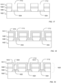
- a similar structure can be formed as illustrated in FIGs. 10-15 .
- sensor pads 1004 can be formed over a CMOS structure 1002.
- An insulation material layer 1006 can be deposited over the sensor pads 1004.
- the insulation material layer 1006 can be formed of an insulation material, such as silicon dioxide, silicon oxynitride, or a combination thereof.
- the insulation material layer 1006 has a thickness in a range of 0.3 micrometers to 1.5 micrometers, such as 0.4 micrometers to 1.0 micrometers, or even a range of 0.4 micrometers to 0.7 micrometers.
- the insulation layer 1006 can be patterned using lithographic method and can be etched to expose the sensor pads 1004. As a result, insulation structures 1108 are formed between the sensor pads 1004.
- a high intrinsic buffer capacity material can be deposited over the structures 1108 and the sensor pads 1004.
- layers of high intrinsic buffer capacity material such as aluminum oxide, hafnium oxide, tantalum oxide, zirconium oxide or a combination thereof, can be deposited over the structures 1108 and the sensor pads 1004.
- a layer 1210 of tantalum oxide can be deposited over the structures 1108 and the sensor pads 1004 and a layer 1212 of aluminum oxide can be deposited over the layer 1210 of tantalum oxide.
- a layer (not illustrated) of aluminum oxide can be deposited between the layer 1210 and the structures 1108 or the sensory pads 1004.
- the layers 1210 or 1212 can have a thickness in a range of 5 nm to 100 nm, such as a range of 10 nm to 70 nm, a range of 15 nm to 65 nm, or even a range of 20 nm to 50 nm.
- one or more layers 1314, 1316, or 1318 of low intrinsic buffer capacity material can be deposited over the layers 1210 or 1212.
- one or more layers silicon oxide, silicon nitride, silicon oxynitride, tetraethoxysilane (TEOS) or a combination thereof can be deposited over the layers 1210 or 1212.
- TEOS tetraethoxysilane
- Such low intrinsic buffer capacity materials can be deposited using TEOS deposition techniques.
- chemical vapor deposition can be used to form such layers.
- one or more of the layers can be formed of a polymer, such as a polyxylylene or a fluoropolymer.
- a layer 1314 of silicon dioxide is deposited over the layers 1210 and 1212.
- a layer 1316 of silicon nitride is deposited over the layer 1314, and a layer 1318 of silicon dioxide is deposited over the layer 1316.
- a high intrinsic buffer capacity material layer 1320 can be deposited over the layer 1318.
- the total thickness of the layers 1314, 1316, or 1318 can be in a range of 1 ⁇ m to 10 ⁇ m, such as a range of 2 ⁇ m to 7 ⁇ m, or even a range of 3 ⁇ m to 5 ⁇ m.
- the layer 1320 can have a thickness in a range of 5 nm to 100 nm, such as a range of 10 nm to 70 nm, a range of 15 nm to 65 nm, or even a range of 20 nm to 50 nm.
- a well 1422 is opened through layers 1314, 1316, 1318, or 1320, as illustrated in FIG. 14 .
- a wet etch process, plasma etch process, or combination thereof can be used to open the well 1422.
- a plasma etch with etch stop detection can be used.
- a fluorinated plasma etch using fluorinated species such as trifluoromethane, tetrafluoromethane, nitrogen fluoride, sulfur hexafluoride, or a combination thereof, can be utilized.
- a wet etch technique can be used to strip the aluminum oxide layer 1212, exposing the tantalum oxide layer 1210 over the sensor pad 1004.
- a similar structure is formed as described in relation to FIG. 9 in which an upper surface 1524 includes a high intrinsic buffer capacity material, a wall surface 1526 is formed of low intrinsic buffer capacity materials, and a lower surface 1528 of the well 1422 includes a high intrinsic buffer capacity material.
- a high intrinsic buffer capacity material can be deposited in a single layer to form an upper surface of the well wall structure and a lower surface associated with the well.
- one or more layers can be deposited over a CMOS structure 1602 and sensor pads 1604.
- the CMOS structure 1602 includes a portion of the sensor device operatively coupled to the sensor pad 1604.
- One or more layers (1606, 1608, or 1610) of low buffer capacity material can be deposited over the sensor pads 1604.
- Exemplary materials include silicon dioxide, silicon nitride, silicon oxynitride, tetraethoxysilane (TEOS) or a combination thereof.
- a layer 1606 of silicon dioxide is deposited over the sensor pads 1604 and the CMOS structure 1602.
- a layer 1608 of silicon nitride is deposited over the layer 1606, and a layer 1610 of silicon dioxide is deposited over the layer 1608.
- the layers 1606, 1608, or 1610 can be formed using chemical vapor deposition (CVD), TEOS deposition through plasma enhanced CVD, a hydrolysis method, or a combination thereof.
- the total thickness of the layers 1606, 1608, or 1610 can be in a range of 0.3 micrometers to 10 micrometers, such as a range of 0.5 micrometers to 6 micrometers.
- the layers 1606, 1608, or 1610 can be patterned using lithographic techniques and can be etched to expose the sensor pads 1604, defining wells 1712.
- etch technique such as wet etch, plasma etch techniques, or a combination thereof, can be used to open the well 1712.
- a fluorinated plasma etch using fluorinated species such as trifluoromethane, tetrafluoromethane, nitrogen fluoride, sulfur hexafluoride, or a combination thereof, can be used.
- a film 1814 of high intrinsic buffer capacity material can be deposited over the etched layers 1606, 1608, or 1610 and the sensor pad 1604, as illustrated in FIG. 18 .
- one or more layers of aluminum oxide, hafnium oxide, tantalum oxide, zirconium oxide, or a combination thereof can be deposited using atomic layer deposition technique.
- a three layer stack including a layer of aluminum oxide over a layer of tantalum oxide over a further layer of aluminum oxide can be deposited to form the film 1814.
- the film 1814 can have a total thickness in a range of 20 nm to 500 nm, such as a range of 20 nm to 300 nm, or even a range of 20 nm to 250 nm.
- each of the layers can have a thickness in a range of 10 nm to 100 nm, such as a thickness in a range of 10 nm to 50 nm, or even a range of 10 nm to 30 nm.
- a three layer stack including 20 nm layers of aluminum oxide, tantalum oxide, and a further layer of aluminum oxide can be deposited using an atomic layer deposition technique.
- a further layer of low intrinsic buffer capacity material can be deposited over the film 1814.
- a layer 1816 including an oxide of silicon can be deposited over the film 1814.
- the layer 1816 can be formed of nitrides of silicon or other low intrinsic buffer capacity materials.
- the layer 1816 has a thickness in a range of 50 nm to 1 micrometer, such as a range of 50 nm to 500 nm, or even a range of 100 nm to 300 nm.
- the silicon dioxide layer can be anisotropic etched to remove portions of the layer 1816 from the top surface of the well structure and the lower surface of the well, leaving portions of the layer 1816 on the well wall, as illustrated in FIG. 19 .
- a wet etch can be used to strip an aluminum oxide layer, leaving an upper surface and a lower surface of exposed tantalum oxide.
- an upper surface 1918 of the well wall structure 1920 and a lower surface 1922 of the well 1712 include an exposed high intrinsic buffer capacity material, while a wall surface 1924 is defined by a low intrinsic buffer capacity oxide of silicon.
- a well wall surface can be formed of a polymeric material, isolating high intrinsic buffer capacity materials from the well wall surface and limiting exposure of the high intrinsic buffer capacity materials to the upper surface of the well wall structure and a lower surface of the well.
- a well 1712 is defined in one or more layers 1606, 1608, or 1610 to expose a sensor pad 1604.
- one or more layers of high buffer capacity material can be deposited as a film 2014.
- the film 2014 can include aluminum oxide, hafnium oxide, tantalum oxide, zirconium oxide, or a combination thereof.
- layers of aluminum oxide and tantalum oxide are deposited using atomic layer deposition.
- a layer of aluminum oxide is deposited over a layer of tantalum oxide, which is deposited over a further layer of aluminum oxide.
- a layer 2016 of an inorganic material, such as a polymeric material is deposited over the film 2014.
- An exemplary polymeric material includes a polymer having an aromatic group in its backbone.
- the polymer can be a poly(xylylene), such as a poly(p-xylylene), including functionalize p-xylylenes, such as halogenated p-xylylenes.
- the polymeric material includes a fluoropolymer.
- An exemplary fluoropolymer includes polytetrafluoroethylene (PTFE), polyvinylidene fluoride (PVDF), polyvinyl fluoride (PVF), fluorinated ethylene propylene (FEP) copolymer, ethylene chlorotrifluoroethylene (ECTFE) copolymer, a copolymer of tetrafluoroethylene, hexafluoropropylene, and vinylidene fluoride (THV), a copolymer of tetrafluoroethylene and perfluoro methylvinylether (PFA or MFA), a fluoropolymer having a fluorinated oxolane in its backbone, perfluoroether, or a combination thereof.
- the fluoropolymer can be a fluoropolymer having fluorinated oxolane in its backbone, for example, Cytop.
- the layer 2016 can be anisotropic wet etched to remove the polymer from an upper surface 2120 of the well wall structure 2118 and the lower surface 2124 of the well 1712.
- the polymeric material remains on the wall surface 2122 of the wells 1712.
- a tantalum oxide layer can be exposed using a wet etch process to remove aluminum oxide.
- well wall structure 2118 includes an upper surface 2120 of exposed high intrinsic buffer capacity material, and lower surface 2124 of the well 1712 is defined by the same high intrinsic buffer capacity material.
- the layer 2016 of polymer forms the wall surface 2122 and isolates the well wall surface 2122 from the high intrinsic buffer capacity material of the film 2014.
- the polymeric material can be substituted with an inorganic material, such as a nitride of silicon or titanium.
- the inorganic material is an electrically conductive material.
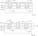
- FIG. 22 illustrates a film 2222 formed of one or more layers of high intrinsic buffer capacity material, such as aluminum oxide, hafnium oxide, tantalum oxide, zirconium oxide, or a combination thereof.
- the film 2222 can be formed as described above with the thicknesses described above.
- a three layer stack including a layer of aluminum oxide over a layer of tantalum oxide, which is disposed over a layer of aluminum oxide, defines the film 2222.
- a layer 2224 of electrically conductive material is deposited over the film 2222.
- the layer 2224 can be formed of a layer of titanium nitride.
- the layer 2224 can be anisotropic wet etched to remove the electrically conductive film 2224 from a top surface 2328 of a well wall structure 2326 and a lower surface 2330 of the well 1712.
- the electrically conductive layer 2224 remains along a wall surface 2332.
- an aluminum oxide layer of the film 2222 can be removed to expose a tantalum oxide layer on both the upper surface 2328 and the lower surface 2330.
- well walls may be formed of a metallic material.
- the metal well walls can be formed using a process similar to a Damascene or dual-Damascene process.
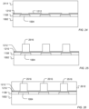
- an oxide layer 2414 can be deposited over layers 1210 or 1212, as illustrated in FIG. 24 .
- the layer 2414 is formed of a material that can be removed using a technique that will not damage or erode metallic layers or structures.
- the layer 2414 can be patterned using lithographic technique and etched to form well posts 2516.
- the well posts 2516 are disposed over the sensor pads 1004.
- a metal layer 2618 can be deposited over the exposed layers 1210 or 1212, in addition to the well post 2516, as illustrated in FIG. 26 .
- the metal layer 2618 can be deposited using an electroplating technique.
- the metal layer 2618 can be deposited using liquid deposition techniques, sputtering, or evaporation techniques.
- the metal layer 2618 can be formed of a metal such as aluminum, copper, titanium, nickel, gold, silver, platinum or any combination thereof.
- the metal layer 2618 can be planarized to expose the well post 2516.
- a chemical mechanical polishing technique can be utilized to planarize the metal layer 2618 and expose the well posts 2516.
- the well posts 2516 can be etched, for example, using a plasma etch technique, such as a reactive ion etch, to remove the well post 2516, leaving the metallic layer 2618 to define wells 2820, as illustrated in FIG. 28 . While not illustrated, the aluminum oxide layer 1212 can be removed using a wet etch technique to expose the tantalum oxide layer 1210 over the sensor pad 1004.
- a plasma etch technique such as a reactive ion etch
- ceramic materials can be used to support metallic layers that define the well wall.
- the layer 2414 can be etched in a pattern.
- the layer 2414 can be patterned using a lithographic technique and etched to form a trench 2918, as illustrated in FIG. 29 .
- a well post 2916 is defined on an opposite side of the trench 2918 from a well wall structure 2914.
- the well post 2916 extends to a greater height over the CMOS structure 1002 than the well wall structure 2914.
- a metal layer 3020 can be deposited over the well wall structure 2914 and the well post 2916 and within the trench 2918.
- the metal layer 3020 be deposited using an electroplating technique.
- the metal layer can be deposited using liquid deposition techniques, sputtering, evaporation techniques, or a combination thereof.
- the metal layer 3020 can be formed of a metal such as aluminum, copper, nickel, gold, platinum, silver, titanium, or a combination thereof.
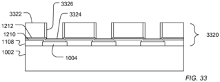
- the metal layer 3020 can be planarized using, for example, chemical mechanical polishing to expose the well posts 2916, leaving a portion of the layer 3020 over the well wall structure 2914, as illustrated in FIG. 31 .
- the well posts 2916 can be etched, removing the well posts 2916 and leaving wells 3224, as illustrated in FIG. 32 .
- an aluminum oxide layer 1212 can be removed using a wet etch process to expose a tantalum oxide layer 1210 disposed over the sensor pad 1004.
- an additional planarization process can be used to remove the metal layer 3020 from the upper surface 3322 of the well wall structure 3320, as illustrated in FIG. 33 .
- the wall surface 3326 is defined by a metallic material
- the lower surface 3324 of the well 3224 is defined by high intrinsic buffer capacity material.
- a passivation layer such as an oxide of tantalum, aluminum, hafnium, or zirconium
- a coating such as those described above in relation to FIG. 3 can be used to enhance sensitivity of the system. Further, exposed upper surfaces of well wall structures can be enhanced with such coatings.
- coatings described above in relation to FIG. 3 that reduce the intrinsic buffer capacity of a surface can be used on the wall surfaces.
- a system in a first aspect in accordance with the teachings of the present disclosure, includes a sensor including a sensor pad and a well wall structure defining a well operatively connected to the sensor pad.
- the sensor pad is associated with a lower surface of the well.
- the well wall structure defines an upper surface and a wall surface extending between the upper surface and the lower surface.
- the upper surface is defined by an upper buffer material having an intrinsic buffer capacity of at least 2 ⁇ l0 17 groups/m 2 .
- the wall surface is defined by a wall material having an intrinsic buffer capacity of not greater than 1.7xl0 17 groups/m 2 .
- the upper buffer material has an intrinsic buffer capacity of at least 4 ⁇ l0 17 groups/m 2 .
- the upper buffer material can have an intrinsic buffer capacity of at least 8 ⁇ l0 17 groups/m2, such as an intrinsic buffer capacity of at least 1 ⁇ l0 18 groups/m 2 , or at least 2 ⁇ l0 18 groups/m 2 .
- the upper buffer material has an intrinsic buffer capacity of not greater than l ⁇ l0 21 groups/m 2 .
- the wall material has an intrinsic buffer capacity of not greater than 1 ⁇ l0 17 groups/m 2 .
- the wall material has an intrinsic buffer capacity of not greater than 5 ⁇ l0 16 groups/m 2 , such as an intrinsic buffer capacity of not greater than 2 ⁇ l0 16 groups/m 2 , not greater than 1 ⁇ l0 16 groups/m 2 , or not greater than 5 ⁇ l0 15 groups/m 2 .
- the lower surface of the well is defined by a lower buffer material disposed over the sensor pad.
- the lower buffer material has an intrinsic buffer capacity of at least 2 ⁇ l0 17 groups/m 2 , such as an intrinsic buffer capacity of at least 4 ⁇ 10 17 groups/m , at least 1 ⁇ 10 18 groups/m , or at least 2 ⁇ 10 18 groups/m 2 .
- the lower buffer material has an intrinsic buffer capacity of not greater than 1 ⁇ l0 21 groups/m 2 .
- the upper buffer material and the lower buffer material are the same.
- the upper buffer material includes an inorganic material.
- the upper buffer material includes a ceramic material.
- the ceramic material includes an oxide of aluminum, hafnium, tantalum, zirconium, or a combination thereof.
- the ceramic material includes an oxide of tantalum.
- the ceramic material includes an oxide of aluminum.
- the wall material includes an inorganic material.
- the inorganic material includes a ceramic material.
- the ceramic material includes a nitride of silica or titanium.
- the ceramic material includes an oxide of silicon.
- the inorganic material includes a metal material.
- the metal material includes aluminum, copper, nickel, titanium, gold, silver, platinum, or a combination thereof.
- the metal material includes copper.
- the wall material includes an organic material.
- the organic material includes a polymeric material.
- the polymeric material includes poly(xylylene).
- the senor and wall structure are integral to an electronic component.
- the electronic component is disposed in cooperation with a flow chamber to place the sensor and the well wall structure in fluid communication with an aqueous solution.
- the electronic component is in signal communication with a processor.
- a method of forming a sensor system includes forming a structural layer over a sensor device.
- the sensor device includes a sensor pad.
- the structural layer includes a structural material having an intrinsic buffer capacity of not greater than 1.7xl0 17 groups/m 2 .
- the method further includes forming a buffer layer over the structural layer.
- the buffer layer includes a buffer material having an intrinsic buffer capacity of at least 2 ⁇ l0 17 groups/m 2 .
- the method also includes etching the buffer layer and the structural layer to define a well operatively connected to the sensor pad.
- the structural material has an intrinsic buffer capacity of not greater than l ⁇ l0 17 groups/m 2 .
- the buffer material has an intrinsic buffer capacity of at least 4 ⁇ l0 17 groups/m 2 .
- the method further includes forming a passivation layer over the sensor pad prior to forming the structural layer, the passivation layer disposed between the sensor device and the structural layer.
- the method further includes forming an etch stop layer over the passivation layer. The etch stop layer is disposed between the structural layer and the passivation layer.
- etching can include exposing the passivation layer.
- forming the structural layer includes forming a first dielectric layer and forming a second dielectric layer, a material of the first dielectric layer being different from a material of the second dielectric layer.
- the method can further include forming a third dielectric layer over the second dielectric layer, a material of the second dielectric layer being different from a material of the third dielectric layer.
- the first dielectric layer can include an oxide of silicon.
- the second dielectric layer can include silicon nitride.
- forming the structural layer includes depositing TEOS.
- a method of sequencing a polynucleotide includes applying a particle comprising a plurality of copies of a polynucleotide to a well of a system of the first aspect, exposing the particle to an aqueous solution including a nucleotide, and measuring a response of the device to the exposing.
- a system in a fourth aspect in accordance with the teachings of the present disclosure, includes a sensor device including a sensor pad and a well wall structure defining a well in operative connection with the sensor pad. A lower surface of the well is defined over the sensor pad.
- the well wall structure has an upper surface and a wall surface extending between the upper surface and the lower surface.
- the system includes a passivation film disposed over the upper surface, the wall surface and the lower surface and an isolation film disposed over the passivation film opposite the well wall structure and extending substantially parallel to and at least along a portion of the wall surface.
- the passivation layer is exposed at least along a portion of the upper surface and at least along a portion of the lower surface.
- the passivation layer includes a buffer material having an intrinsic buffer capacity of at least 2xl0 17 groups/m 2 .
- the buffer material includes an oxide of zirconium, aluminum, tantalum, hafnium, or a combination thereof.
- the buffer material includes an oxide of tantalum.
- the isolation layer includes a low buffer material having an intrinsic buffer capacity of not greater than 1.7xl0 17 groups/m2.
- the low buffer material includes a ceramic material.
- the low buffer material includes an oxide of silicon.
- the low buffer material includes a nitride of silicon, titanium, or a combination thereof.
- the low buffer material includes a polymeric material.
- the polymeric material include poly(xylylene).
- a method of forming a sensor system includes forming a structural layer over a sensor device, the sensor device including a sensor pad and etching the structural layer to define a well operatively connected to the sensor pad. A lower surface of the well is defined over the sensor pad.
- the structurally layer has an upper surface and a wall surface extending between the upper surface and the lower surface.
- the method includes forming a passivation film over the structural layer. The passivation film extends along at least a portion of the upper surface and extends over the wall surface and the lower surface.
- the method further includes forming an isolation film over the passivation film and etching the isolation film to expose the passivation film along at least the portion of the upper surface and at least a portion of the lower surface.
- forming the structural layer includes forming a first dielectric layer and forming a second dielectric layer, a material of the first dielectric layer being different from a material of the second dielectric layer.
- the method further includes forming a third dielectric layer over the second dielectric layer, a material of the second dielectric layer being different from a material of the third dielectric layer.
- the first dielectric layer includes an oxide of silicon.
- the second dielectric layer includes silicon nitride.
- forming the structural layer includes depositing TEOS.
- forming the passivation layer includes depositing a buffer material having an intrinsic buffer capacity of at least 2 ⁇ l0 17 groups/m 2 .
- forming the passivation layer includes depositing an oxide of aluminum, zirconium, hafnium, tantalum, or a combination thereof.
- forming the isolation layer includes depositing an inorganic material.
- the inorganic material includes a nitride of titanium, silicon, or a combination thereof.
- forming the isolation layer includes depositing a polymeric material.
- the polymeric material includes a poly(xylylene).
- etching the isolation material includes anisotropic etching the isolation material.
- a method of sequencing a polynucleotide includes applying a particle comprising a plurality of copies of a polynucleotide to a well of a system of the fourth aspect, exposing the particle to an aqueous solution including a nucleotide, and measuring a response of the device to the exposing.
- a system in an example not forming part of the invention, includes a sensor device including a sensor pad and a well wall structure defining a well in operative connection with the sensor pad.
- a lower surface of the well is defined over the sensor pad.
- the well wall structure has an upper surface, and a wall surface extends between the upper surface and the lower surface.
- a metal layer is disposed over the well wall structure and extends along the upper surface and the wall surface.
- the metal layer includes aluminum, copper, nickel, gold, silver, titanium, platinum, or a combination thereof.
- the metal layer can include copper.
- the lower surface is free of the metal layer.
- the wall surface extends substantially vertically.
- the well wall structure includes an inorganic material.
- the inorganic material includes a ceramic material.
- the ceramic material includes a nitride of silica or titanium.
- the ceramic material includes an oxide of silicon.
- a method of forming a sensor system includes forming a structural layer over a sensor device, the sensor device including a sensor pad, and etching the structural layer to form a trench defining a well post over the senor pad and a well wall structure opposite the first structure, the well post extending vertically higher than the well wall structure.
- the method further includes depositing a metal layer into the trench and over the well post and the well wall structure, exposing the well post, and etching to remove the well post.
- a method of forming a sensor system includes forming a structural layer over a sensor device, the sensor device including a sensor pad, etching the structural layer to form a well post over the senor pad, depositing a metal layer to surround the well post, and etching to remove the well post.
- a method of sequencing a polynucleotide includes applying a particle comprising a plurality of copies of a polynucleotide to a well of a system of the example not forming part of the invention, exposing the particle to an aqueous solution including a nucleotide, and measuring a response of the device to the exposing.
- over or overlie refers to a position away from a surface relative to a normal direction from the surface.
- the terms “over” or “overlie” are intended to permit intervening layers or direct contact with an underlying layer. As described above, layers that are disposed over or overlie another layer can be in direct contact with the identified layer or can include intervening layers.
- the terms “comprises,” “comprising,” “includes,” “including,” “has,” “having” or any other variation thereof, are intended to cover a non-exclusive inclusion.
- a process, method, article, or apparatus that comprises a list of features is not necessarily limited only to those features but may include other features not expressly listed or inherent to such process, method, article, or apparatus.
- “or” refers to an inclusive-or and not to an exclusive-or. For example, a condition A or B is satisfied by any one of the following: A is true (or present) and B is false (or not present), A is false (or not present) and B is true (or present), and both A and B are true (or present).
- references to values stated in ranges include each and every value within that range.
Landscapes
- Chemical & Material Sciences (AREA)
- Health & Medical Sciences (AREA)
- Life Sciences & Earth Sciences (AREA)
- Physics & Mathematics (AREA)
- General Health & Medical Sciences (AREA)
- Chemical Kinetics & Catalysis (AREA)
- Analytical Chemistry (AREA)
- Molecular Biology (AREA)
- Immunology (AREA)
- General Physics & Mathematics (AREA)
- Biochemistry (AREA)
- Electrochemistry (AREA)
- Pathology (AREA)
- Microelectronics & Electronic Packaging (AREA)
- Engineering & Computer Science (AREA)
- Clinical Laboratory Science (AREA)
- Hematology (AREA)
- Dispersion Chemistry (AREA)
- Spectroscopy & Molecular Physics (AREA)
- Computer Hardware Design (AREA)
- Apparatus Associated With Microorganisms And Enzymes (AREA)
- Pressure Sensors (AREA)
Claims (12)
- System (300), umfassend:einen Sensor (214), der ein Sensorpad (306, 1604) einschließt, wobei der Sensor ein chemischer Feldeffekttransistor ist;eine Vertiefungswandstruktur (302, 2118, 2326), die eine Vertiefung (304) in Wirkverbindung mit dem Sensorpad definiert, wobei eine untere Oberfläche (308) der Vertiefung über dem Sensorpad definiert ist, wobei die Vertiefungswandstruktur eine obere Oberfläche (310) und eine Wandoberfläche (312) aufweist, die sich zwischen der oberen Oberfläche und der unteren Oberfläche erstreckt;eine Passivierungsschicht (1814, 2014, 2222), die über der oberen Oberfläche, der Wandoberfläche und der unteren Oberfläche angeordnet ist; undeine Isolierschicht (1816, 2016 und 2224), die über der Passivierungsschicht gegenüber der Vertiefungswandstruktur angeordnet ist und sich im Wesentlichen parallel zu und mindestens entlang eines Abschnitts der Wandoberfläche erstreckt, wobei die Passivierungsschicht mindestens entlang eines Abschnitts der oberen Oberfläche und mindestens entlang eines Abschnitts der unteren Oberfläche freigelegt ist, wobei die Passivierungsschicht ein Material mit hohem Puffer einschließt, das eine intrinsische Pufferkapazität von mindestens 2 × 10¹⁷ Gruppen/m2 aufweist,und wobei die Isolierschicht ein Material mit geringem Puffer einschließt, das eine intrinsische Pufferkapazität von nicht mehr als 1,7 × 10¹⁷ Gruppen/m2 aufweist, wobei die intrinsische Pufferkapazität als die Oberflächendichte von Hydroxylgruppen auf einer Oberfläche eines Materials gemessen bei einem pH-Wert von 7 definiert ist.
- System (300) nach Anspruch 1, wobei das Material mit hohem Puffer ein Oxid von Zirkonium, Aluminium, Tantal, Hafnium oder einer Kombination davon einschließt.
- System (300) nach Anspruch 2, wobei das Material mit hohem Puffer ein Oxid von Tantal einschließt.
- System (300) nach Anspruch 1, wobei das Material mit niedrigem Puffer ein Keramikmaterial einschließt.
- System (300) nach Anspruch 4, wobei das Material mit geringem Puffer ein Oxid von Silizium einschließt.
- System (300) nach Anspruch 4, wobei das Material mit geringem Puffer ein Nitrid von Silizium, Titan oder einer Kombination davon einschließt.
- System (300) nach Anspruch 1, wobei das Material mit geringem Puffer ein polymeres Material einschließt.
- System (300) nach Anspruch 7, wobei das polymere Material Poly(xylylen) einschließt.
- Verfahren zum Ausbilden eines Sensorsystems (300), das Verfahren umfassend:Ausbilden einer Strukturschicht über einer Sensorvorrichtung (214), der Sensorvorrichtung, wobei die Sensorvorrichtung ein chemischer Feldeffekttransistor ist, wobei die Sensorvorrichtung ein Sensorpad (306, 1604) einschließt;Ätzen der Strukturschicht, um eine Vertiefung zu definieren, die mit dem Sensorpad wirkverbunden ist, wobei eine untere Oberfläche der Vertiefung (308) über dem Sensorpad definiert ist, wobei die Strukturschicht eine obere Oberfläche (310) und eine Wandoberfläche (312) aufweist, die sich zwischen der oberen Oberfläche und der unteren Oberfläche erstreckt,Ausbilden einer Passivierungsschicht (1814, 2014, 2222) über der Strukturschicht, wobei sich die Passivierungsschicht entlang mindestens eines Abschnitts der oberen Oberfläche erstreckt und sich über die Wandoberfläche und die untere Oberfläche erstreckt,Ausbilden einer Isolierschicht (1816, 2016, 2224) über der Passivierungsschicht; undÄtzen der Isolierschicht, um die Passivierungsschicht entlang mindestens des Abschnitts der oberen Oberfläche und mindestens eines Abschnitts der unteren Oberfläche freizulegen, wobei das Ausbilden der Passivierungsschicht ein Auftragen eines Materials mit hohem Puffer einschließt, das eine intrinsische Pufferkapazität von mindestens 2 × 10¹⁷ Gruppen/m2 aufweist, und wobei die Isolierschicht ein Material mit geringem Puffer einschließt, das eine intrinsische Pufferkapazität von nicht mehr als 1,7 × 10¹⁷ Gruppen/m2 aufweist, wobei die intrinsische Pufferkapazität als die Oberflächendichte von Hydroxylgruppen auf einer Oberfläche eines Materials gemessen bei einem pH-Wert von 7 definiert ist.
- Verfahren nach Anspruch 9, wobei das Ausbilden der Strukturschicht das Ausbilden einer ersten dielektrischen Schicht und das Ausbilden einer zweiten dielektrischen Schicht einschließt, wobei sich ein Material der ersten dielektrischen Schicht von einem Material der zweiten dielektrischen Schicht unterscheidet.
- Verfahren nach Anspruch 10, ferner umfassend das Ausbilden einer dritten dielektrischen Schicht über der zweiten dielektrischen Schicht, wobei sich ein Material der zweiten dielektrischen Schicht von einem Material der dritten dielektrischen Schicht unterscheidet.
- Verfahren nach einem der Ansprüche 9 bis 11, wobei das Ausbilden der Passivierungsschicht das Abscheiden eines Oxids von Aluminium, Zirkonium, Hafnium, Tantal oder einer Kombination davon einschließt.
Applications Claiming Priority (2)
| Application Number | Priority Date | Filing Date | Title |
|---|---|---|---|
| US13/354,088 US9194840B2 (en) | 2012-01-19 | 2012-01-19 | Sensor arrays and methods for making same |
| PCT/US2013/021622 WO2013109559A1 (en) | 2012-01-19 | 2013-01-16 | System and manufacturing method of the system comprising a sensor array and a well wall structure over the sensor array |
Publications (2)
| Publication Number | Publication Date |
|---|---|
| EP2805156A1 EP2805156A1 (de) | 2014-11-26 |
| EP2805156B1 true EP2805156B1 (de) | 2023-11-29 |
Family
ID=47714519
Family Applications (1)
| Application Number | Title | Priority Date | Filing Date |
|---|---|---|---|
| EP13704258.6A Active EP2805156B1 (de) | 2012-01-19 | 2013-01-16 | System und herstellungsverfahren für das system mit einer sensoranordnung und einer microwell-struktur auf der sensoranordnung |
Country Status (3)
| Country | Link |
|---|---|
| US (2) | US9194840B2 (de) |
| EP (1) | EP2805156B1 (de) |
| WO (1) | WO2013109559A1 (de) |
Families Citing this family (34)
| Publication number | Priority date | Publication date | Assignee | Title |
|---|---|---|---|---|
| EP2588851B1 (de) | 2010-06-30 | 2016-12-21 | Life Technologies Corporation | Ion-sensing charge-accumulation circuit and method |
| TWI465716B (zh) | 2010-06-30 | 2014-12-21 | 生命技術公司 | 用於檢測及測量化學反應及化合物之電晶體電路 |
| US11307166B2 (en) | 2010-07-01 | 2022-04-19 | Life Technologies Corporation | Column ADC |
| JP5959516B2 (ja) | 2010-08-18 | 2016-08-02 | ライフ テクノロジーズ コーポレーション | 電気化学的検出装置のためのマイクロウェルの化学コーティング法 |
| US9970984B2 (en) | 2011-12-01 | 2018-05-15 | Life Technologies Corporation | Method and apparatus for identifying defects in a chemical sensor array |
| US9841398B2 (en) * | 2013-01-08 | 2017-12-12 | Life Technologies Corporation | Methods for manufacturing well structures for low-noise chemical sensors |
| CN105264366B (zh) | 2013-03-15 | 2019-04-16 | 生命科技公司 | 具有一致传感器表面区域的化学传感器 |
| US10458942B2 (en) | 2013-06-10 | 2019-10-29 | Life Technologies Corporation | Chemical sensor array having multiple sensors per well |
| US9476853B2 (en) | 2013-12-10 | 2016-10-25 | Life Technologies Corporation | System and method for forming microwells |
| US9895715B2 (en) | 2014-02-04 | 2018-02-20 | Asm Ip Holding B.V. | Selective deposition of metals, metal oxides, and dielectrics |
| US10047435B2 (en) | 2014-04-16 | 2018-08-14 | Asm Ip Holding B.V. | Dual selective deposition |
| KR102593647B1 (ko) | 2014-12-18 | 2023-10-26 | 라이프 테크놀로지스 코포레이션 | 트랜스미터 구성을 갖춘 높은 데이터율 집적 회로 |
| US9490145B2 (en) | 2015-02-23 | 2016-11-08 | Asm Ip Holding B.V. | Removal of surface passivation |
| KR102699712B1 (ko) | 2015-03-05 | 2024-08-29 | 라이프 테크놀로지스 코포레이션 | 바이오센서의 표면 안정화 |
| US10428421B2 (en) | 2015-08-03 | 2019-10-01 | Asm Ip Holding B.V. | Selective deposition on metal or metallic surfaces relative to dielectric surfaces |
| US10048220B2 (en) * | 2015-10-08 | 2018-08-14 | Taiwan Semiconductor Manufacturing Company Ltd. | Biosensor field effect transistor having specific well structure and method of forming the same |
| US10814349B2 (en) | 2015-10-09 | 2020-10-27 | Asm Ip Holding B.V. | Vapor phase deposition of organic films |
| US10695794B2 (en) | 2015-10-09 | 2020-06-30 | Asm Ip Holding B.V. | Vapor phase deposition of organic films |
| US11081342B2 (en) | 2016-05-05 | 2021-08-03 | Asm Ip Holding B.V. | Selective deposition using hydrophobic precursors |
| US10373820B2 (en) | 2016-06-01 | 2019-08-06 | Asm Ip Holding B.V. | Deposition of organic films |
| US10453701B2 (en) | 2016-06-01 | 2019-10-22 | Asm Ip Holding B.V. | Deposition of organic films |
| US11430656B2 (en) | 2016-11-29 | 2022-08-30 | Asm Ip Holding B.V. | Deposition of oxide thin films |
| US11094535B2 (en) | 2017-02-14 | 2021-08-17 | Asm Ip Holding B.V. | Selective passivation and selective deposition |
| US11501965B2 (en) | 2017-05-05 | 2022-11-15 | Asm Ip Holding B.V. | Plasma enhanced deposition processes for controlled formation of metal oxide thin films |
| JP7183187B2 (ja) | 2017-05-16 | 2022-12-05 | エーエスエム アイピー ホールディング ビー.ブイ. | 誘電体上の酸化物の選択的peald |
| WO2019246279A1 (en) * | 2018-06-22 | 2019-12-26 | Magarray, Inc. | Magnetic sensors with a mixed oxide passivation layer |
| JP2020056104A (ja) | 2018-10-02 | 2020-04-09 | エーエスエム アイピー ホールディング ビー.ブイ. | 選択的パッシベーションおよび選択的堆積 |
| US12482648B2 (en) | 2018-10-02 | 2025-11-25 | Asm Ip Holding B.V. | Selective passivation and selective deposition |
| US10746691B1 (en) | 2019-02-21 | 2020-08-18 | International Business Machines Corporation | Ion-sensitive field effect transistor (ISFET) with enhanced sensitivity |
| US11965238B2 (en) | 2019-04-12 | 2024-04-23 | Asm Ip Holding B.V. | Selective deposition of metal oxides on metal surfaces |
| US11139163B2 (en) | 2019-10-31 | 2021-10-05 | Asm Ip Holding B.V. | Selective deposition of SiOC thin films |
| TWI865747B (zh) | 2020-03-30 | 2024-12-11 | 荷蘭商Asm Ip私人控股有限公司 | 在兩不同表面上同時選擇性沉積兩不同材料 |
| TW202140832A (zh) | 2020-03-30 | 2021-11-01 | 荷蘭商Asm Ip私人控股有限公司 | 氧化矽在金屬表面上之選擇性沉積 |
| TWI862807B (zh) | 2020-03-30 | 2024-11-21 | 荷蘭商Asm Ip私人控股有限公司 | 相對於金屬表面在介電表面上之氧化矽的選擇性沉積 |
Family Cites Families (54)
| Publication number | Priority date | Publication date | Assignee | Title |
|---|---|---|---|---|
| US4425384A (en) | 1981-04-27 | 1984-01-10 | Shell Oil Company | Polymer-reinforcing compositions and their preparation |
| US4480005A (en) | 1981-04-27 | 1984-10-30 | Shell Oil Company | Thin layer thermoplastic polymer bonded covalently at its surface to a mineral component |
| US4629779A (en) | 1983-10-27 | 1986-12-16 | Union Carbide Corporation | Low viscosity adducts of a polycaprolactone polyol and a polyepoxide |
| US4599401A (en) | 1983-10-27 | 1986-07-08 | Union Carbide Corporation | Low viscosity adducts of poly(active hydrogen) organic compounds and a polyepoxide |
| US4626570A (en) | 1984-06-29 | 1986-12-02 | Union Carbide Corporation | Low shrinking thermosetting polyester resin compositions and a process for the preparation thereof |
| US4522978A (en) | 1984-06-29 | 1985-06-11 | Union Carbide Corporation | Low viscosity, dicyclopentadienyl-modified polyester compositions and a process for the preparation thereof |
| US4522977A (en) | 1984-06-29 | 1985-06-11 | Union Carbide Corporation | Process for producing dicyclopentadienyl-modified polyester compositions |
| US4532297A (en) | 1984-06-29 | 1985-07-30 | Union Carbide Corporation | Low viscosity curable polyester resin compositions and a process for the production thereof |
| US4532296A (en) | 1984-06-29 | 1985-07-30 | Union Carbide Corporation | Process for producing low viscosity curable polyester resin compositions |
| US4683202A (en) | 1985-03-28 | 1987-07-28 | Cetus Corporation | Process for amplifying nucleic acid sequences |
| US4965188A (en) | 1986-08-22 | 1990-10-23 | Cetus Corporation | Process for amplifying, detecting, and/or cloning nucleic acid sequences using a thermostable enzyme |
| US4683195A (en) | 1986-01-30 | 1987-07-28 | Cetus Corporation | Process for amplifying, detecting, and/or-cloning nucleic acid sequences |
| US4800159A (en) | 1986-02-07 | 1989-01-24 | Cetus Corporation | Process for amplifying, detecting, and/or cloning nucleic acid sequences |
| CA2020958C (en) | 1989-07-11 | 2005-01-11 | Daniel L. Kacian | Nucleic acid sequence amplification methods |
| US5112456A (en) | 1989-12-12 | 1992-05-12 | Trustees Of The University Of Pennsylvania | Electrochemical sensors and methods for their use |
| US6054034A (en) | 1990-02-28 | 2000-04-25 | Aclara Biosciences, Inc. | Acrylic microchannels and their use in electrophoretic applications |
| US5126022A (en) | 1990-02-28 | 1992-06-30 | Soane Tecnologies, Inc. | Method and device for moving molecules by the application of a plurality of electrical fields |
| US5210015A (en) | 1990-08-06 | 1993-05-11 | Hoffman-La Roche Inc. | Homogeneous assay system using the nuclease activity of a nucleic acid polymerase |
| JP3080178B2 (ja) | 1991-02-18 | 2000-08-21 | 東洋紡績株式会社 | 核酸配列の増幅方法およびそのための試薬キット |
| US5587128A (en) | 1992-05-01 | 1996-12-24 | The Trustees Of The University Of Pennsylvania | Mesoscale polynucleotide amplification devices |
| US5498392A (en) | 1992-05-01 | 1996-03-12 | Trustees Of The University Of Pennsylvania | Mesoscale polynucleotide amplification device and method |
| US6001229A (en) | 1994-08-01 | 1999-12-14 | Lockheed Martin Energy Systems, Inc. | Apparatus and method for performing microfluidic manipulations for chemical analysis |
| US5854033A (en) | 1995-11-21 | 1998-12-29 | Yale University | Rolling circle replication reporter systems |
| JP4540754B2 (ja) | 1996-06-04 | 2010-09-08 | ユニバーシティ オブ ユタ リサーチ ファウンデーション | Pcr中のハイブリダイゼーションのモニタリング |
| US6074827A (en) | 1996-07-30 | 2000-06-13 | Aclara Biosciences, Inc. | Microfluidic method for nucleic acid purification and processing |
| AU1517999A (en) | 1997-10-15 | 1999-05-03 | Aclara Biosciences, Inc. | Laminate microstructure device and method for making same |
| JP4262799B2 (ja) | 1998-04-16 | 2009-05-13 | 平田機工株式会社 | 生タイヤ供給方法 |
| US7548787B2 (en) | 2005-08-03 | 2009-06-16 | Kamilo Feher | Medical diagnostic and communication system |
| JP3815969B2 (ja) | 1999-05-12 | 2006-08-30 | アクララ バイオサイエンシーズ, インコーポレイテッド | 微量流体デバイスにおける多重方式蛍光検出 |
| US6939451B2 (en) | 2000-09-19 | 2005-09-06 | Aclara Biosciences, Inc. | Microfluidic chip having integrated electrodes |
| EP1384022A4 (de) | 2001-04-06 | 2004-08-04 | California Inst Of Techn | Nukleinsäure-amplifikation verwendende mikrofluidvorrichtungen |
| US7049645B2 (en) | 2001-11-16 | 2006-05-23 | Bio-X Inc. | FET type sensor, ion density detecting method comprising this sensor, and base sequence detecting method |
| US7504364B2 (en) | 2002-03-01 | 2009-03-17 | Receptors Llc | Methods of making arrays and artificial receptors |
| US7462512B2 (en) | 2004-01-12 | 2008-12-09 | Polytechnic University | Floating gate field effect transistors for chemical and/or biological sensing |
| JP3903183B2 (ja) | 2004-02-03 | 2007-04-11 | 独立行政法人物質・材料研究機構 | 遺伝子検出電界効果デバイスおよびこれを用いた遺伝子多型解析方法 |
| ITTO20040386A1 (it) | 2004-06-09 | 2004-09-09 | Infm Istituto Naz Per La Fisi | Dispositivo ad effetto di campo per la rilevazione di piccole quantita' di carica elettrica, come quelle generate in processi biomolecolari, immobilizzate nelle vicinanze della superficie. |
| US7190026B2 (en) | 2004-08-23 | 2007-03-13 | Enpirion, Inc. | Integrated circuit employable with a power converter |
| WO2006022370A1 (ja) | 2004-08-27 | 2006-03-02 | National Institute For Materials Science | 電界効果デバイスを用いたdna塩基配列解析方法及び塩基配列解析装置 |
| WO2006041224A1 (en) | 2004-10-14 | 2006-04-20 | Kabushiki Kaisha Toshiba | Fet-based nucleic acid detecting sensor |
| JP4232108B2 (ja) | 2005-05-20 | 2009-03-04 | セイコーエプソン株式会社 | 標的物質の検出または定量方法、該方法に用いられる電極基板、装置、およびキット |
| JP4353958B2 (ja) | 2005-09-15 | 2009-10-28 | 株式会社日立製作所 | Dna計測装置、及びdna計測方法 |
| JP4857820B2 (ja) | 2006-03-03 | 2012-01-18 | 学校法人早稲田大学 | Dnaセンシング方法 |
| JP5001015B2 (ja) | 2006-09-28 | 2012-08-15 | 富士フイルム株式会社 | 非特異吸着を抑制した表面を有する生化学用器具 |
| GB2457851B (en) | 2006-12-14 | 2011-01-05 | Ion Torrent Systems Inc | Methods and apparatus for measuring analytes using large scale fet arrays |
| US7932034B2 (en) | 2006-12-20 | 2011-04-26 | The Board Of Trustees Of The Leland Stanford Junior University | Heat and pH measurement for sequencing of DNA |
| JP5027296B2 (ja) | 2007-04-27 | 2012-09-19 | エヌエックスピー ビー ヴィ | バイオセンサチップ |
| GB2461127B (en) | 2008-06-25 | 2010-07-14 | Ion Torrent Systems Inc | Methods and apparatus for measuring analytes using large scale FET arrays |
| ES2522346T3 (es) | 2008-08-22 | 2014-11-14 | Novartis Ag | Compuestos de pirrolopirimidina como inhibidores de CDK |
| CN103901090B (zh) | 2008-10-22 | 2017-03-22 | 生命技术公司 | 用于生物和化学分析的集成式传感器阵列 |
| US20100301398A1 (en) * | 2009-05-29 | 2010-12-02 | Ion Torrent Systems Incorporated | Methods and apparatus for measuring analytes |
| US20100137143A1 (en) | 2008-10-22 | 2010-06-03 | Ion Torrent Systems Incorporated | Methods and apparatus for measuring analytes |
| US8673627B2 (en) | 2009-05-29 | 2014-03-18 | Life Technologies Corporation | Apparatus and methods for performing electrochemical reactions |
| US8653567B2 (en) | 2010-07-03 | 2014-02-18 | Life Technologies Corporation | Chemically sensitive sensor with lightly doped drains |
| JP5959516B2 (ja) * | 2010-08-18 | 2016-08-02 | ライフ テクノロジーズ コーポレーション | 電気化学的検出装置のためのマイクロウェルの化学コーティング法 |
-
2012
- 2012-01-19 US US13/354,088 patent/US9194840B2/en active Active
-
2013
- 2013-01-16 WO PCT/US2013/021622 patent/WO2013109559A1/en not_active Ceased
- 2013-01-16 EP EP13704258.6A patent/EP2805156B1/de active Active
-
2015
- 2015-09-23 US US14/863,173 patent/US9528962B2/en active Active
Also Published As
| Publication number | Publication date |
|---|---|
| US20130189790A1 (en) | 2013-07-25 |
| US9528962B2 (en) | 2016-12-27 |
| EP2805156A1 (de) | 2014-11-26 |
| US20160011146A1 (en) | 2016-01-14 |
| US9194840B2 (en) | 2015-11-24 |
| WO2013109559A1 (en) | 2013-07-25 |
Similar Documents
| Publication | Publication Date | Title |
|---|---|---|
| EP2805156B1 (de) | System und herstellungsverfahren für das system mit einer sensoranordnung und einer microwell-struktur auf der sensoranordnung | |
| US8747748B2 (en) | Chemical sensor with conductive cup-shaped sensor surface | |
| US12487238B2 (en) | Capacitive sensor and method of use | |
| US9023674B2 (en) | Biosensing well array with protective layer | |
| EP2140256B1 (de) | Biosensorchip | |
| EP2237027B1 (de) | Sensorvorrichtung und Verfahren zu dessen Herstellung | |
| US20210102917A1 (en) | Deep microwell designs and methods of making the same | |
| US20170108464A1 (en) | System and method for forming microwells | |
| US20220196595A1 (en) | Chemical sensor with air via | |
| US20220381728A1 (en) | Sensing assembly, system and method for determining a property |
Legal Events
| Date | Code | Title | Description |
|---|---|---|---|
| PUAI | Public reference made under article 153(3) epc to a published international application that has entered the european phase |
Free format text: ORIGINAL CODE: 0009012 |
|
| 17P | Request for examination filed |
Effective date: 20140813 |
|
| AK | Designated contracting states |
Kind code of ref document: A1 Designated state(s): AL AT BE BG CH CY CZ DE DK EE ES FI FR GB GR HR HU IE IS IT LI LT LU LV MC MK MT NL NO PL PT RO RS SE SI SK SM TR |
|
| DAX | Request for extension of the european patent (deleted) | ||
| RAP1 | Party data changed (applicant data changed or rights of an application transferred) |
Owner name: LIFE TECHNOLOGIES CORPORATION |
|
| STAA | Information on the status of an ep patent application or granted ep patent |
Free format text: STATUS: EXAMINATION IS IN PROGRESS |
|
| 17Q | First examination report despatched |
Effective date: 20181008 |
|
| GRAP | Despatch of communication of intention to grant a patent |
Free format text: ORIGINAL CODE: EPIDOSNIGR1 |
|
| STAA | Information on the status of an ep patent application or granted ep patent |
Free format text: STATUS: GRANT OF PATENT IS INTENDED |
|
| RIC1 | Information provided on ipc code assigned before grant |
Ipc: G01N 27/414 20060101AFI20210222BHEP Ipc: B01L 3/00 20060101ALI20210222BHEP Ipc: G01N 33/543 20060101ALI20210222BHEP Ipc: G01N 27/27 20060101ALN20210222BHEP Ipc: C12M 1/32 20060101ALI20210222BHEP |
|
| RIC1 | Information provided on ipc code assigned before grant |
Ipc: G01N 27/414 20060101AFI20210301BHEP Ipc: G01N 27/27 20060101ALN20210301BHEP Ipc: B01L 3/00 20060101ALI20210301BHEP Ipc: C12M 1/32 20060101ALI20210301BHEP Ipc: G01N 33/543 20060101ALI20210301BHEP |
|
| INTG | Intention to grant announced |
Effective date: 20210317 |
|
| GRAJ | Information related to disapproval of communication of intention to grant by the applicant or resumption of examination proceedings by the epo deleted |
Free format text: ORIGINAL CODE: EPIDOSDIGR1 |
|
| STAA | Information on the status of an ep patent application or granted ep patent |
Free format text: STATUS: EXAMINATION IS IN PROGRESS |
|
| INTC | Intention to grant announced (deleted) | ||
| REG | Reference to a national code |
Ref country code: DE Ref legal event code: R079 Free format text: PREVIOUS MAIN CLASS: G01N0027270000 Ipc: G01N0027414000 Ref country code: DE Ref legal event code: R079 Ref document number: 602013084986 Country of ref document: DE Free format text: PREVIOUS MAIN CLASS: G01N0027270000 Ipc: G01N0027414000 |
|
| GRAP | Despatch of communication of intention to grant a patent |
Free format text: ORIGINAL CODE: EPIDOSNIGR1 |
|
| STAA | Information on the status of an ep patent application or granted ep patent |
Free format text: STATUS: GRANT OF PATENT IS INTENDED |
|
| RIC1 | Information provided on ipc code assigned before grant |
Ipc: G01N 27/27 20060101ALN20230606BHEP Ipc: B01L 3/00 20060101ALI20230606BHEP Ipc: G01N 33/543 20060101ALI20230606BHEP Ipc: C12M 1/32 20060101ALI20230606BHEP Ipc: G01N 27/414 20060101AFI20230606BHEP |
|
| INTG | Intention to grant announced |
Effective date: 20230621 |
|
| GRAS | Grant fee paid |
Free format text: ORIGINAL CODE: EPIDOSNIGR3 |
|
| GRAA | (expected) grant |
Free format text: ORIGINAL CODE: 0009210 |
|
| STAA | Information on the status of an ep patent application or granted ep patent |
Free format text: STATUS: THE PATENT HAS BEEN GRANTED |
|
| AK | Designated contracting states |
Kind code of ref document: B1 Designated state(s): AL AT BE BG CH CY CZ DE DK EE ES FI FR GB GR HR HU IE IS IT LI LT LU LV MC MK MT NL NO PL PT RO RS SE SI SK SM TR |
|
| REG | Reference to a national code |
Ref country code: GB Ref legal event code: FG4D |
|
| REG | Reference to a national code |
Ref country code: CH Ref legal event code: EP |
|
| REG | Reference to a national code |
Ref country code: DE Ref legal event code: R096 Ref document number: 602013084986 Country of ref document: DE |
|
| REG | Reference to a national code |
Ref country code: IE Ref legal event code: FG4D |
|
| P01 | Opt-out of the competence of the unified patent court (upc) registered |
Effective date: 20231208 |
|
| REG | Reference to a national code |
Ref country code: LT Ref legal event code: MG9D |
|
| REG | Reference to a national code |
Ref country code: NL Ref legal event code: MP Effective date: 20231129 |
|
| PG25 | Lapsed in a contracting state [announced via postgrant information from national office to epo] |
Ref country code: GR Free format text: LAPSE BECAUSE OF FAILURE TO SUBMIT A TRANSLATION OF THE DESCRIPTION OR TO PAY THE FEE WITHIN THE PRESCRIBED TIME-LIMIT Effective date: 20240301 |
|
| PG25 | Lapsed in a contracting state [announced via postgrant information from national office to epo] |
Ref country code: IS Free format text: LAPSE BECAUSE OF FAILURE TO SUBMIT A TRANSLATION OF THE DESCRIPTION OR TO PAY THE FEE WITHIN THE PRESCRIBED TIME-LIMIT Effective date: 20240329 |
|
| PG25 | Lapsed in a contracting state [announced via postgrant information from national office to epo] |
Ref country code: LT Free format text: LAPSE BECAUSE OF FAILURE TO SUBMIT A TRANSLATION OF THE DESCRIPTION OR TO PAY THE FEE WITHIN THE PRESCRIBED TIME-LIMIT Effective date: 20231129 |
|
| PG25 | Lapsed in a contracting state [announced via postgrant information from national office to epo] |
Ref country code: ES Free format text: LAPSE BECAUSE OF FAILURE TO SUBMIT A TRANSLATION OF THE DESCRIPTION OR TO PAY THE FEE WITHIN THE PRESCRIBED TIME-LIMIT Effective date: 20231129 |
|
| PG25 | Lapsed in a contracting state [announced via postgrant information from national office to epo] |
Ref country code: LT Free format text: LAPSE BECAUSE OF FAILURE TO SUBMIT A TRANSLATION OF THE DESCRIPTION OR TO PAY THE FEE WITHIN THE PRESCRIBED TIME-LIMIT Effective date: 20231129 Ref country code: IS Free format text: LAPSE BECAUSE OF FAILURE TO SUBMIT A TRANSLATION OF THE DESCRIPTION OR TO PAY THE FEE WITHIN THE PRESCRIBED TIME-LIMIT Effective date: 20240329 Ref country code: GR Free format text: LAPSE BECAUSE OF FAILURE TO SUBMIT A TRANSLATION OF THE DESCRIPTION OR TO PAY THE FEE WITHIN THE PRESCRIBED TIME-LIMIT Effective date: 20240301 Ref country code: ES Free format text: LAPSE BECAUSE OF FAILURE TO SUBMIT A TRANSLATION OF THE DESCRIPTION OR TO PAY THE FEE WITHIN THE PRESCRIBED TIME-LIMIT Effective date: 20231129 Ref country code: BG Free format text: LAPSE BECAUSE OF FAILURE TO SUBMIT A TRANSLATION OF THE DESCRIPTION OR TO PAY THE FEE WITHIN THE PRESCRIBED TIME-LIMIT Effective date: 20240229 |
|
| REG | Reference to a national code |
Ref country code: AT Ref legal event code: MK05 Ref document number: 1636624 Country of ref document: AT Kind code of ref document: T Effective date: 20231129 |
|
| PG25 | Lapsed in a contracting state [announced via postgrant information from national office to epo] |
Ref country code: NL Free format text: LAPSE BECAUSE OF FAILURE TO SUBMIT A TRANSLATION OF THE DESCRIPTION OR TO PAY THE FEE WITHIN THE PRESCRIBED TIME-LIMIT Effective date: 20231129 |
|
| PG25 | Lapsed in a contracting state [announced via postgrant information from national office to epo] |
Ref country code: SE Free format text: LAPSE BECAUSE OF FAILURE TO SUBMIT A TRANSLATION OF THE DESCRIPTION OR TO PAY THE FEE WITHIN THE PRESCRIBED TIME-LIMIT Effective date: 20231129 Ref country code: RS Free format text: LAPSE BECAUSE OF FAILURE TO SUBMIT A TRANSLATION OF THE DESCRIPTION OR TO PAY THE FEE WITHIN THE PRESCRIBED TIME-LIMIT Effective date: 20231129 Ref country code: PL Free format text: LAPSE BECAUSE OF FAILURE TO SUBMIT A TRANSLATION OF THE DESCRIPTION OR TO PAY THE FEE WITHIN THE PRESCRIBED TIME-LIMIT Effective date: 20231129 Ref country code: NO Free format text: LAPSE BECAUSE OF FAILURE TO SUBMIT A TRANSLATION OF THE DESCRIPTION OR TO PAY THE FEE WITHIN THE PRESCRIBED TIME-LIMIT Effective date: 20240229 Ref country code: NL Free format text: LAPSE BECAUSE OF FAILURE TO SUBMIT A TRANSLATION OF THE DESCRIPTION OR TO PAY THE FEE WITHIN THE PRESCRIBED TIME-LIMIT Effective date: 20231129 Ref country code: LV Free format text: LAPSE BECAUSE OF FAILURE TO SUBMIT A TRANSLATION OF THE DESCRIPTION OR TO PAY THE FEE WITHIN THE PRESCRIBED TIME-LIMIT Effective date: 20231129 Ref country code: HR Free format text: LAPSE BECAUSE OF FAILURE TO SUBMIT A TRANSLATION OF THE DESCRIPTION OR TO PAY THE FEE WITHIN THE PRESCRIBED TIME-LIMIT Effective date: 20231129 |
|
| PG25 | Lapsed in a contracting state [announced via postgrant information from national office to epo] |
Ref country code: DK Free format text: LAPSE BECAUSE OF FAILURE TO SUBMIT A TRANSLATION OF THE DESCRIPTION OR TO PAY THE FEE WITHIN THE PRESCRIBED TIME-LIMIT Effective date: 20231129 |
|
| PG25 | Lapsed in a contracting state [announced via postgrant information from national office to epo] |
Ref country code: CZ Free format text: LAPSE BECAUSE OF FAILURE TO SUBMIT A TRANSLATION OF THE DESCRIPTION OR TO PAY THE FEE WITHIN THE PRESCRIBED TIME-LIMIT Effective date: 20231129 Ref country code: AT Free format text: LAPSE BECAUSE OF FAILURE TO SUBMIT A TRANSLATION OF THE DESCRIPTION OR TO PAY THE FEE WITHIN THE PRESCRIBED TIME-LIMIT Effective date: 20231129 |
|
| PG25 | Lapsed in a contracting state [announced via postgrant information from national office to epo] |
Ref country code: SK Free format text: LAPSE BECAUSE OF FAILURE TO SUBMIT A TRANSLATION OF THE DESCRIPTION OR TO PAY THE FEE WITHIN THE PRESCRIBED TIME-LIMIT Effective date: 20231129 |
|
| PG25 | Lapsed in a contracting state [announced via postgrant information from national office to epo] |
Ref country code: SM Free format text: LAPSE BECAUSE OF FAILURE TO SUBMIT A TRANSLATION OF THE DESCRIPTION OR TO PAY THE FEE WITHIN THE PRESCRIBED TIME-LIMIT Effective date: 20231129 Ref country code: SK Free format text: LAPSE BECAUSE OF FAILURE TO SUBMIT A TRANSLATION OF THE DESCRIPTION OR TO PAY THE FEE WITHIN THE PRESCRIBED TIME-LIMIT Effective date: 20231129 Ref country code: RO Free format text: LAPSE BECAUSE OF FAILURE TO SUBMIT A TRANSLATION OF THE DESCRIPTION OR TO PAY THE FEE WITHIN THE PRESCRIBED TIME-LIMIT Effective date: 20231129 Ref country code: IT Free format text: LAPSE BECAUSE OF FAILURE TO SUBMIT A TRANSLATION OF THE DESCRIPTION OR TO PAY THE FEE WITHIN THE PRESCRIBED TIME-LIMIT Effective date: 20231129 Ref country code: EE Free format text: LAPSE BECAUSE OF FAILURE TO SUBMIT A TRANSLATION OF THE DESCRIPTION OR TO PAY THE FEE WITHIN THE PRESCRIBED TIME-LIMIT Effective date: 20231129 Ref country code: DK Free format text: LAPSE BECAUSE OF FAILURE TO SUBMIT A TRANSLATION OF THE DESCRIPTION OR TO PAY THE FEE WITHIN THE PRESCRIBED TIME-LIMIT Effective date: 20231129 Ref country code: CZ Free format text: LAPSE BECAUSE OF FAILURE TO SUBMIT A TRANSLATION OF THE DESCRIPTION OR TO PAY THE FEE WITHIN THE PRESCRIBED TIME-LIMIT Effective date: 20231129 Ref country code: AT Free format text: LAPSE BECAUSE OF FAILURE TO SUBMIT A TRANSLATION OF THE DESCRIPTION OR TO PAY THE FEE WITHIN THE PRESCRIBED TIME-LIMIT Effective date: 20231129 |
|
| PG25 | Lapsed in a contracting state [announced via postgrant information from national office to epo] |
Ref country code: PT Free format text: LAPSE BECAUSE OF FAILURE TO SUBMIT A TRANSLATION OF THE DESCRIPTION OR TO PAY THE FEE WITHIN THE PRESCRIBED TIME-LIMIT Effective date: 20240401 |
|
| PG25 | Lapsed in a contracting state [announced via postgrant information from national office to epo] |
Ref country code: MC Free format text: LAPSE BECAUSE OF FAILURE TO SUBMIT A TRANSLATION OF THE DESCRIPTION OR TO PAY THE FEE WITHIN THE PRESCRIBED TIME-LIMIT Effective date: 20231129 |
|
| PG25 | Lapsed in a contracting state [announced via postgrant information from national office to epo] |
Ref country code: PT Free format text: LAPSE BECAUSE OF FAILURE TO SUBMIT A TRANSLATION OF THE DESCRIPTION OR TO PAY THE FEE WITHIN THE PRESCRIBED TIME-LIMIT Effective date: 20240401 Ref country code: MC Free format text: LAPSE BECAUSE OF FAILURE TO SUBMIT A TRANSLATION OF THE DESCRIPTION OR TO PAY THE FEE WITHIN THE PRESCRIBED TIME-LIMIT Effective date: 20231129 |
|
| REG | Reference to a national code |
Ref country code: DE Ref legal event code: R097 Ref document number: 602013084986 Country of ref document: DE Ref country code: CH Ref legal event code: PL |
|
| PG25 | Lapsed in a contracting state [announced via postgrant information from national office to epo] |
Ref country code: LU Free format text: LAPSE BECAUSE OF NON-PAYMENT OF DUE FEES Effective date: 20240116 |
|
| PG25 | Lapsed in a contracting state [announced via postgrant information from national office to epo] |
Ref country code: LU Free format text: LAPSE BECAUSE OF NON-PAYMENT OF DUE FEES Effective date: 20240116 |
|
| PLBE | No opposition filed within time limit |
Free format text: ORIGINAL CODE: 0009261 |
|
| STAA | Information on the status of an ep patent application or granted ep patent |
Free format text: STATUS: NO OPPOSITION FILED WITHIN TIME LIMIT |
|
| PG25 | Lapsed in a contracting state [announced via postgrant information from national office to epo] |
Ref country code: BE Free format text: LAPSE BECAUSE OF NON-PAYMENT OF DUE FEES Effective date: 20240131 |
|
| PG25 | Lapsed in a contracting state [announced via postgrant information from national office to epo] |
Ref country code: CH Free format text: LAPSE BECAUSE OF NON-PAYMENT OF DUE FEES Effective date: 20240131 |
|
| PG25 | Lapsed in a contracting state [announced via postgrant information from national office to epo] |
Ref country code: SI Free format text: LAPSE BECAUSE OF FAILURE TO SUBMIT A TRANSLATION OF THE DESCRIPTION OR TO PAY THE FEE WITHIN THE PRESCRIBED TIME-LIMIT Effective date: 20231129 |
|
| PG25 | Lapsed in a contracting state [announced via postgrant information from national office to epo] |
Ref country code: SI Free format text: LAPSE BECAUSE OF FAILURE TO SUBMIT A TRANSLATION OF THE DESCRIPTION OR TO PAY THE FEE WITHIN THE PRESCRIBED TIME-LIMIT Effective date: 20231129 Ref country code: CH Free format text: LAPSE BECAUSE OF NON-PAYMENT OF DUE FEES Effective date: 20240131 Ref country code: BE Free format text: LAPSE BECAUSE OF NON-PAYMENT OF DUE FEES Effective date: 20240131 |
|
| REG | Reference to a national code |
Ref country code: BE Ref legal event code: MM Effective date: 20240131 |
|
| 26N | No opposition filed |
Effective date: 20240830 |
|
| PG25 | Lapsed in a contracting state [announced via postgrant information from national office to epo] |
Ref country code: IE Free format text: LAPSE BECAUSE OF NON-PAYMENT OF DUE FEES Effective date: 20240116 |
|
| PG25 | Lapsed in a contracting state [announced via postgrant information from national office to epo] |
Ref country code: IE Free format text: LAPSE BECAUSE OF NON-PAYMENT OF DUE FEES Effective date: 20240116 |
|
| PG25 | Lapsed in a contracting state [announced via postgrant information from national office to epo] |
Ref country code: CY Free format text: LAPSE BECAUSE OF FAILURE TO SUBMIT A TRANSLATION OF THE DESCRIPTION OR TO PAY THE FEE WITHIN THE PRESCRIBED TIME-LIMIT; INVALID AB INITIO Effective date: 20130116 |
|
| PG25 | Lapsed in a contracting state [announced via postgrant information from national office to epo] |
Ref country code: HU Free format text: LAPSE BECAUSE OF FAILURE TO SUBMIT A TRANSLATION OF THE DESCRIPTION OR TO PAY THE FEE WITHIN THE PRESCRIBED TIME-LIMIT; INVALID AB INITIO Effective date: 20130116 |
|
| PG25 | Lapsed in a contracting state [announced via postgrant information from national office to epo] |
Ref country code: FI Free format text: LAPSE BECAUSE OF FAILURE TO SUBMIT A TRANSLATION OF THE DESCRIPTION OR TO PAY THE FEE WITHIN THE PRESCRIBED TIME-LIMIT Effective date: 20231129 |
|
| PG25 | Lapsed in a contracting state [announced via postgrant information from national office to epo] |
Ref country code: TR Free format text: LAPSE BECAUSE OF FAILURE TO SUBMIT A TRANSLATION OF THE DESCRIPTION OR TO PAY THE FEE WITHIN THE PRESCRIBED TIME-LIMIT Effective date: 20231129 |
|
| PGFP | Annual fee paid to national office [announced via postgrant information from national office to epo] |
Ref country code: GB Payment date: 20260109 Year of fee payment: 14 |
|
| PGFP | Annual fee paid to national office [announced via postgrant information from national office to epo] |
Ref country code: DE Payment date: 20251211 Year of fee payment: 14 |
|
| PGFP | Annual fee paid to national office [announced via postgrant information from national office to epo] |
Ref country code: FR Payment date: 20260114 Year of fee payment: 14 |