EP2804319B1 - Dynamische Pegelschieberschaltung - Google Patents
Dynamische Pegelschieberschaltung Download PDFInfo
- Publication number
- EP2804319B1 EP2804319B1 EP14368024.7A EP14368024A EP2804319B1 EP 2804319 B1 EP2804319 B1 EP 2804319B1 EP 14368024 A EP14368024 A EP 14368024A EP 2804319 B1 EP2804319 B1 EP 2804319B1
- Authority
- EP
- European Patent Office
- Prior art keywords
- power domain
- input
- output
- signal
- memory element
- Prior art date
- Legal status (The legal status is an assumption and is not a legal conclusion. Google has not performed a legal analysis and makes no representation as to the accuracy of the status listed.)
- Active
Links
Images





Classifications
-
- H—ELECTRICITY
- H03—ELECTRONIC CIRCUITRY
- H03K—PULSE TECHNIQUE
- H03K3/00—Circuits for generating electric pulses; Monostable, bistable or multistable circuits
- H03K3/02—Generators characterised by the type of circuit or by the means used for producing pulses
- H03K3/353—Generators characterised by the type of circuit or by the means used for producing pulses by the use, as active elements, of field-effect transistors with internal or external positive feedback
- H03K3/356—Bistable circuits
- H03K3/356104—Bistable circuits using complementary field-effect transistors
- H03K3/356182—Bistable circuits using complementary field-effect transistors with additional means for controlling the main nodes
-
- H—ELECTRICITY
- H03—ELECTRONIC CIRCUITRY
- H03K—PULSE TECHNIQUE
- H03K3/00—Circuits for generating electric pulses; Monostable, bistable or multistable circuits
- H03K3/02—Generators characterised by the type of circuit or by the means used for producing pulses
- H03K3/353—Generators characterised by the type of circuit or by the means used for producing pulses by the use, as active elements, of field-effect transistors with internal or external positive feedback
- H03K3/356—Bistable circuits
- H03K3/356104—Bistable circuits using complementary field-effect transistors
- H03K3/356113—Bistable circuits using complementary field-effect transistors using additional transistors in the input circuit
- H03K3/35613—Bistable circuits using complementary field-effect transistors using additional transistors in the input circuit the input circuit having a differential configuration
-
- H—ELECTRICITY
- H03—ELECTRONIC CIRCUITRY
- H03K—PULSE TECHNIQUE
- H03K19/00—Logic circuits, i.e. having at least two inputs acting on one output; Inverting circuits
- H03K19/0175—Coupling arrangements; Interface arrangements
- H03K19/0185—Coupling arrangements; Interface arrangements using field effect transistors only
- H03K19/018592—Coupling arrangements; Interface arrangements using field effect transistors only with a bidirectional operation
-
- H—ELECTRICITY
- H03—ELECTRONIC CIRCUITRY
- H03K—PULSE TECHNIQUE
- H03K3/00—Circuits for generating electric pulses; Monostable, bistable or multistable circuits
- H03K3/01—Details
- H03K3/012—Modifications of generator to improve response time or to decrease power consumption
Definitions
- the present document relates to electronic circuits.
- the present document relates to dynamic level shifter circuits utilizing coupling capacitances and cross coupled latches.
- Level shifters are converting an input signal e.g. from a first operating voltage range having a first ground potential and a first supply potential into an output signal out in a second operating voltage range having a second ground potential and a second supply potential.
- input VDD regulated to 5V
- Vpwr can be regulated by an LDO that is supplied (connected) to Vpwr voltage.
- Vpwr can be directly connected to the unregulated battery voltage (one/two/three cell battery voltages) for example with specification of 4.2 - 12.6V if connected together.
- VSS2 can be also regulated, for example (Vpwr -5V). During operation as battery voltage (Vpwr) decay VSS2 can approach regulated VDD or it can be below VDD if VDD is supplied externally. Conventional level shifters may stop operation under such conditions.
- US 2008/0317106 discloses an Integrated circuit comprising a first microcontroller unit for executing instructions in accordance with a first clock frequency.
- the microcontroller is located on a first die and includes a first processing core for providing a parallel stream of data in accordance with the first clock frequency.
- a second microcontroller unit executes instructions in accordance with the first clock frequency.
- the second microcontroller is located on a second die and includes a second processing core for receiving the parallel stream of data in accordance with the first clock frequency.
- Capacitive isolation circuitry connected with the first microcontroller unit and the second microcontroller unit provides a high voltage Isolation link between the first and the second microcontroller milts.
- the capacitive isolation circuitry distributing a first portion of a high voltage isolation signal across a first group of capacitors associated with the first microcontroller unit and distributes a second portion of the high voltage isolation signal across a second group of capacitors associated with the second microcontroller unit.
- the capacitive Isolation circuitry further transmits data from the parallel data stream between the first microcontroller and the second microcontroller in a serial data stream in accordance with the second clock frequency.
- a principal object of the present disclosure is to design a dynamic level shifter having no DC (standby) consumption.
- a further object of the disclosure is to achieve fast operation with low propagation delay.
- a further object of the disclosure is to achieve unrestricted (flexible) input-output power voltages domains
- a further object of the disclosure is to achieve DC isolation between power domains.
- a further object of the disclosure is to achieve symmetrical rise/fall times without signal or duty cycle distortions.
- an object of the disclosure is to reduce over-voltage stress by deploying metal-insulator-metal capacitors or any other suitable capacitor type.
- an object of the disclosure is to avoid using high-voltage (HV) devices for level shifting purpose.
- HV high-voltage
- an object of the disclosure is to deploy level shifting capacitors and cross-coupled latches.
- an object of the disclosure is to reduce over-voltage stress by deploying metal-insulator-metal capacitors or any other suitable capacitor type.
- an object of the disclosure is to avoid using high-voltage (HV) devices for level shifting purpose.
- HV high-voltage
- an object of the invention is to continue operation of the level shifter when input and output voltage domains do not relate to each other.
- Level shifting circuits and methods are disclosed. Preferred embodiments described in detail comprise level shifters applied in high voltage power systems.
- level shifters is not limited to high voltage power systems.
- Presented level shifting method and apparatus can be used also in deep sub-micron technologies to provide effective level-shifting between power domains or any other system requiring level shifting.
- a dynamic level shifter 10 disclosed is illustrated in Fig. 1 .
- Level shifting is achieved by charging and discharging level shifting capacitors C1 and C2 between input VDD and GND terminals. Capacitors C1 and C2 are charged by the input signal buffers/inverters 1 and 2.
- Input signal IN is a signal referenced to VDD and GND levels.
- the output signals OUT and OUTB are referenced to Vpwr and VSS2 power domain.
- the first terminals of the level shifting capacitors C1 and C2 are connected to the input signals via buffers/inverters 1 and 2.
- the second terminals of the level shifting capacitors C1 and C2 are connected to the latch 5 formed by the cross coupled P1, P2 and N1, N2 devices.
- latch 5 shown in Fig. 1 is an example only. Other types of latches, e.g. the type of latch shown in Fig. 6 , could be used as well.
- Latch P1, P2 and N1, N2 is required to have reset, it is not shown in circuit diagram of Fig. 1 for simplicity.
- Outputs of the latch are buffered through inverters 3 and 4 in the Vpwr/VSS2 domain.
- Fig. 8 shows a similar level shifter is shown for reverse operation from VPwr/VSS2 to VDD/GND.
- the main function of the latch is to hold output state of the last transition of the input signal.
- the input signal is coupled to the latch and once input transitions from one state (for example from 0 to 1) this state will be coupled to the output latch and the latch will hold and not change this state until next transition of the input signal.
- levels shifting capacitors C1 and C2 may be implemented for example by metal capacitors or any other appropriate types of capacitor that can withstand overstress voltage (i.e. Vpwr).
- the proposed dynamic level shifter is able to continue operation even in case VSS2 voltage approaches VDD voltage or falls below VDD as illustrated in Fig. 5 .
- FIG. 6 A more general schematic of the proposed level shifter method is shown in Fig. 6 .
- a latch formed by the cross-coupled P1, P2 and N1, N2 devices from Fig.1 is replaced by a more general representation of latch 64 comprising two inverters O_INV1 60 and O_INV2 61.
- This schematic shows a more general description of the proposed circuit.
- the input power domain VDD/ GND 62 and the output power domain Vpwr/ VSS2 63 are indicated by dotted lines and power supplies are omitted for clarity.
- the latch shown in Fig. 1 has been implemented in Fig. 6 by two inverters. Functionality has been also confirmed by simulation. Similar implementation can be shown for a reverse level shifter as shown in Fig. 10 .
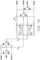
- FIG. 10 illustrates a simplified circuit diagram of a dynamic level shifter disclosed performing reverse operation of the present disclosure. While in the circuit shown in Fig. 1 the input signal IN ranges between VDD and Ground voltage levels ranges the input signal IN of the circuit of Fig. 10 between Vpwr and VSS2 voltage levels. Accordingly range the output signals of the circuit of Fig. 10 between VDD and GND.
- the components of the circuit of Fig. 10 i.e. inverters 1-4, capacitors C1 and C2, and the latch 5 are deployed the same way as in the circuit of Fig. 1 .
- Bidirectional input/output (I/O) Level-shifter can be configured to level shift signals between two power domains.
- Inverters 701 and 78 are each connected to a corresponding signal input port of the power domain VDD/GND. Furthermore the power domain VDD/GND comprises a memory element, as e.g. a latch 705 comprising two converters 70 and 71, connected to level shifting capacitors C1 and C2. Outputs of the latch are buffered through inverters 700 and 79 in the VDD/GND domain Inverters 700 and 79 are each connected to a corresponding signal output port of the power domain VDD/GND.
- a memory element as e.g. a latch 705 comprising two converters 70 and 71, connected to level shifting capacitors C1 and C2. Outputs of the latch are buffered through inverters 700 and 79 in the VDD/GND domain Inverters 700 and 79 are each connected to a corresponding signal output port of the power domain VDD/GND.
- the Vpwr/VSS2 power domain has a symmetrical structure to the VDD/GND power domain but it is supplied by Vpwr and VSS2 voltage.
- the power domain Vpwr/VSS2 also comprises a memory element, as e.g. a latch 704 comprising two converters 72 and 73, connected to, in regard of VDD/GND power domain, opposite terminals of the level shifting capacitors C1 and C2.
- An enable signal EN signal is used to change direction of level shifting. In one direction the EN signal enables inverters 75, 76, 78, and 701 and the inverted EN signal disables inverters 74, 77 , 79, and 700, in the other direction the inverted EN signal enables vice versa inverters 74, 77, 79, and 700 and disables correspondently inverters 75, 76, 78, and 701.
- the VDD/GND 702 power domain and the Vpwr/VSS2 703 power domain are shown.
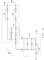
- Fig. 11 illustrates a simplified circuit diagram of a one-way dynamic level shifter disclosed having latches at the input terminal and at the output terminals of the level-shifting capacitors.
- the level shifter 700 comprises an input power domain 720 and an output power domain 730.
- the power supplies of both power domains 720 and 730, corresponding to the power supplies shown in Fig. 1 are not shown in Fig. 11 in order to avoid unnecessary complexity of the drawing.
- the level shifter 700 of Fig. 11 comprises an input port IN connected to the input buffering/inverting means 712, which is connected to a memory element 710.
- the memory element 710 is carried out by a latch 710
- buffering/inverting means 712 is been carried out by two inverters connected in series, wherein the output of a first inverter is connected to a first terminal the latch 710 and to the input terminal of the first level shifting capacitor C1 and the output of the second inverter is connected to a second terminal of the latch 710 and to the input terminal of the second level shifting capacitor C2.
- the output terminal of the first level shifting capacitor C1 is connected to a first terminal of the memory element 711 and to an input of the output buffering means 713 of a first output branch of the level shifter 700.
- the output terminal of the second level shifting capacitor C2 is connected to a first terminal of the memory element 711 and to an input of the output buffering means 714 of a second output branch of the level shifter 700.
- the memory element 711 is carried out by a latch 711, and the buffering/inverting means 713 /714 are been carried out by two inverters connected in series.
- Fig. 2 shows simulation results of the level shifter 10 showing input and output signals for full scale PWM modulated input ramp and level shifter reset signals.
- Diagram 20 shows input signals ranging from 0 - 5 Volts
- diagram 21 shows output signals ranging from 7-12 Volts.
- Fig, 3 depicts simulation results of the level shifter 10 showing input and output signals for full scale PWM modulated input ramp and signals on bottom and top plate of the level shifting capacitors.
- Diagram 30 shows input signals ranging from 0 - 5 Volts
- diagram 31 shows output signals ranging from 7-12 Volts.
- Diagram 32 shows the signals on the bottom plate of capacitor C1, ranging from 0 - 5 Volts
- diagram 34 shows the signals on the bottom plate of capacitor C2, ranging also from 0 - 5 Volts
- diagram 33 shows the signals on the top plate of capacitor C1, ranging from 7-12 Volts
- diagram 35 shows the signals on the top plate of capacitor C2, ranging from 7-12 Volts.
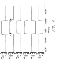
- Fig. 4 illustrates simulation results of the level shifter 10 showing transient response time between input and output signals and signals on bottom and top plate of the level shifting capacitors.
- Diagram 40 shows input signals ranging from 0 - 5 Volts
- diagram 41 shows output signals ranging from 7-12 Volts.
- Comparing diagrams 40 and diagram 41 at points of the rising edges of the input and output pulses indicated show a transient time of 696.235 picosecs while the voltage rises from 2.600V to 6.623 V. Furthermore comparing diagrams 40 and diagram 41 at points of the falling edges of the input and output pulses indicated show a transient time of 698.235 picosecs while the voltage falls from maximum 11.5 V to 6.8077 V. This means the output pulse follows the falling edge of the input pulse with a delay of about ⁇ 1 nsec.
- Diagram 42 shows the signals on the bottom plate of capacitor C1, ranging from 0 - 5 Volts
- diagram 44 shows the signals on the bottom plate of capacitor C2, ranging also from 0 - 5 Volts
- diagram 43 shows the signals on the top plate of capacitor C1, ranging from 7-12 Volts
- diagram 45 shows the signals on the top plate of capacitor C2, ranging from 7-12 Volts.
- Diagram 50 shows the input signals ranging from 0 - 5 Volts
- diagram 51 shows the output signals ramping down and up again accordingly to the ramping of Vpwr. This time chart shows clearly the circuit disclosed allows variations of VSS2 even below VDD voltage.
- Fig. 5 clearly demonstrates a major advantage of the dynamic level shifter.
- the Vpwr is being ramped down from 20 ⁇ sec to about 120 ⁇ sec. It was held low at 5V same as VDD for another 30 ⁇ sec and it started to ramp up from 150 ⁇ sec to 250 ⁇ sec to original value of 12V.
- VSS2 in this example has been always constant Vpwr - 5.5V except from 120 ⁇ sec to 150 ⁇ sec where VSS2 was held to ground.
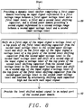
- FIG. 8 illustrates a flowchart of a method to achieve a dynamic level shifter utilizing level shifting capacitors.
- a first step 80 describes provision of a dynamic level shifter comprising a first power domain receiving a first signal referenced to a first voltage range between a first upper voltage level and a first lower level, a first and a second level shifting capacitor, and a second power domain providing a second signal referenced to a second voltage range between a second upper voltage level and a second lower voltage level.
- Step 81 shows shifting on a first edge of the input signal a voltage level of a top plate of the first level shifting capacitor from the second lower voltage level to the second upper voltage level and shifting the same time on the first edge of the input signal a voltage level of a top plate of the second level shifting capacitor from the second upper voltage level to the second lower voltage level and shifting on a second edge of the input signal a voltage level of the top plate of the second level shifting capacitor from the second lower voltage level to the second upper voltage level and shifting the same time on a second edge of the input signal a voltage level of the top plate of the first level shifting capacitor from the second upper voltage level to the second lower voltage level and continue by alternately shifting each capacitor high and low with each input signal edge.
- Step 82 shows providing the level shifted output signal to an output port of the second power domain.
- FIG. 9 illustrates a flowchart of a method to achieve a bi-directional dynamic level shifter utilizing level shifting capacitors.
- a first step 90 describes provision of a dynamic level shifter comprising a first power domain and second power domain, each power domain is configured to receiving an input signal or providing an output signal, wherein the input or output signals of the first power domain are referenced to a first voltage range between a first upper voltage level and a first lower level and the signals of the second power domain are referenced to a second voltage range between a second upper voltage level and a second lower level, wherein both power domains are connected by a first level shifting capacitor and a second level shifting capacitor.
- Step 91 shows shifting alternately each level shifting capacitor with each edge of the input signal from the upper voltage level to a lower voltage level or from a lower voltage level to the upper voltage of the output power domain.
- Step 92 shows providing the level shifted output signal to an output port to the output power domain.
Landscapes
- Engineering & Computer Science (AREA)
- Computer Hardware Design (AREA)
- Physics & Mathematics (AREA)
- Computing Systems (AREA)
- General Engineering & Computer Science (AREA)
- Mathematical Physics (AREA)
- Logic Circuits (AREA)
Claims (15)
- Eine Schaltung, die zur dynamischen bidirektionalen Pegelverschiebung fähig ist, umfassend:- eine erste (702) und eine zweite Leistungsdomäne (703), wobei die Versorgungsspannungen jeder der beiden Leistungsdomänen unterschiedlich sind, wobei jede Leistungsdomäne in der Lage ist, Eingangssignale (IN, INS) zu empfangen, die durch kapazitive Kopplung beider Leistungsdomänen pegelverschoben und durch die andere Leistungsdomäne ausgegeben werden, oder Ausgangssignale (OUT, OUTB) bereitzustellen, die durch die andere Leistungsdomäne eingegeben und durch die kapazitive Kopplung beider Leistungsdomänen pegelverschoben wurden, wobei jede Leistungsdomäne umfasst:- zwei Ports (VDD, GND; Vpwr, VSS2) für die Versorgungsspannung jeder Domäne;- zwei Ports für Eingangssignale (IN, INS), wobei jeder Port für Eingangssignale mit einem Eingang eines eigenen Eingangspuffermittels (701, 78; 77, 74) der jeweiligen Domäne (702, 703) verbunden ist;- die beiden Eingangspuffermittel (701, 78); 77, 74), die in der Lage sind, die Eingangssignale zu puffern, wobei eine erste Puffereinrichtung für Eingangssignale mit einem ersten Anschluss eines Speicherelements (704, 705) des jeweiligen Leistungsdomänes und eine zweite Puffereinrichtung für Eingangssignale mit einem zweiten Anschluss des Speicherelements des jeweiligen Leistungsdomänes verbunden ist;- zwei Anschlüsse (OUT, OUTB) für Ausgangssignale, wobei jeder Anschluss für Signalausgänge mit einem Ausgang einer eigenen Ausgangspuffereinrichtung (700, 79; 76, 75) verbunden ist;- die beiden Ausgangspuffermittel (700, 79; 76, 75), die in der Lage sind, die Ausgangssignale zu puffern, wobei ein erstes Puffermittel für Ausgangssignale mit einem ersten Anschluss des Speicherelements (705, 704) der jeweiligen Leistungsdomäne verbunden ist und ein zweites Puffermittel für Ausgangssignale mit einem zweiten Anschluss des Speicherelements (705, 704) der jeweiligen Leistungsdomäne verbunden ist; und- das Speicherelement (704, 705) der jeweiligen Leistungsdomäne, das in der Lage ist, einen Zustand eines letzten Übergangs eines Eingangs- oder eines Ausgangssignals zu halten, wobei das Speicherelement (705) der ersten Leistungsdomäne (702) in der Lage ist, den Zustand des letzten Übergangs eines Eingangssignals in die erste Leistungsdomäne (702) zu halten, und, sobald das Eingangssignal in den ersten Leistungsdomäne in einen neuen Zustand übergeht, wird der neue Zustand über eine kapazitive Kopplung (C1, C2) an das Speicherelement (704) der zweiten Leistungsdomäne (703) übertragen, wobei das Ausgangssignal und das Speicherelement (704) der zweiten Leistungsdomäne (703) gehalten werden und diesen Zustand nicht ändern, bis ein nächster Übergang des Eingangssignals erfolgt, wobei das Speicherelement (704) der zweiten Leistungsdomäne mit den Puffermitteln der zweiten Leistungsdomäne (703) verbunden ist und wobei das Speicherelement (704) der zweiten Leistungsdomäne (703) in der Lage ist, den Zustand des letzten Übergangs eines Eingangssignals in die zweite Leistungsdomäne (703) aufrechtzuerhalten, und sobald das Eingangssignal in die zweite Leistungsdomäne (703) in einen neuen Zustand übergeht, wird der neue Zustand über eine kapazitive Kopplung (C1, C2) an das Speicherelement (705) der ersten Leistungsdomäne (702) übertragen, das das Ausgangssignal bereitstellt, und das Speicherelement der ersten Leistungsdomäne (702) hält diesen Zustand und ändert ihn nicht, bis ein nächster Übergang eintritt und der erste Anschluss jedes Speicherelements ist mit einem ersten einzelnen Kondensator (C1) der kapazitiven Kopplung verbunden und der zweite Anschluss jedes Speicherelements ist mit einem zweiten einzelnen Kondensator (C2) der kapazitiven Kopplung verbunden;- der erste einzelne Kondensator (C1) ist konfiguriert, um die ersten Anschlüsse der Speicherelemente (704, 705) beider Leistungsdomänen zu entkoppeln; und- der zweite einzelne Kondensator (C2) ist konfiguriert, um die zweiten Anschlüsse der Speicherelemente beider Leistungsdomänen zu entkoppeln; wobei die Eingangs- und Ausgangssignale beider Leistungsdomänen konfiguriert sind, um zwischen einem oberen (VDD, Vpwr) und einem unteren Pegel (GND, Vss2) der Versorgungsspannung des jeweiligen Leistungsdomäne zu wechseln.
- Schaltung nach Anspruch 1, wobei jedes der Speicherelemente umfasst: ein Latch (705, 704), das in der Lage ist, einen Zustand eines letzten Übergangs eines Eingangs- oder eines Ausgangssignals aufrechtzuerhalten, wobei eine erste Klemme des Latches mit einem Ausgangsanschluss eines Inverters (701; 77) der jeweiligen Leistungsdomäne verbunden ist und mit einem ersten Signaleingangsport (IN) der jeweiligen Leistungsdomäne und mit einem Eingangsanschluss eines Inverters (700, 76) verbunden ist, die mit einem ersten Signalausgangsport (OUT) der jeweiligen Leistungsdomäne verbunden ist, und wobei ein zweiter Anschluss des Latches mit einem Ausgangsanschluss eines Inverters (78; 74) der jeweiligen Leistungsdomäne verbunden ist und mit einem zweiten Signaleingangsport (INS) der jeweiligen Leistungsdomäne und mit einem Eingangsanschluss eines Inverters (79; 75) verbunden ist, der mit einem zweiten Signalausgangsport (OUTB) der jeweiligen Leistungsdomäne verbunden ist.
- Schaltung nach Anspruch 1, wobei jedes Speicherelement (705; 704) zwei Inverter (70; 71) umfasst, wobei ein erster Inverter (70) des Latches einen Eingang aufweist, der mit dem ersten Anschluss des Speicherelements verbunden ist, und einen Ausgang, der mit dem zweiten Anschluss des Speicherelements verbunden ist, und der zweite Inverter (71) des Latches einen Eingang aufweist, der mit dem zweiten Anschluss des Speicherelements verbunden ist, und einen Ausgang, der mit dem ersten Anschluss des Speicherelements verbunden ist.
- Schaltung nach Anspruch 1, wobei die Puffermittel jeweils einen Inverter umfassen, wobei Inverter (700, 78, 77, 74), die mit Signaleingangsports einer Leistungsdomäne verbunden sind, die eine Ausgabe bereitstellt, deaktiviert sind, Inverter, die mit Signalausgangsports der Leistungsdomäne verbunden sind, die eine Ausgabe bereitstellt, aktiviert sind, Inverter, die mit Signaleingangsports einer Leistungsdomäne, die eine Eingabe empfängt, verbunden sind, aktiviert sind, und Inverter, die mit Signalausgangsports der Leistungsdomäne, die eine Eingabe empfängt verbunden sind, deaktiviert sind.
- Schaltung nach Anspruch 2, wobei jede Latch (705, 704) ein Paar kreuzgekoppelter P-Transistoren und ein Paar kreuzgekoppelter n-Transistoren umfasst, wobei die Paare parallel geschaltet sind.
- Schaltung nach Anspruch 2, wobei jede Latch (705, 704) zwei Inverter umfasst, wobei ein erster Inverter der Latch einen Eingang aufweist, der mit dem ersten Anschluss der Latch verbunden ist, und einen Ausgang, der mit dem zweiten Anschluss der Latch verbunden ist, und der zweite Inverter der Latch einen Eingang aufweist, der mit dem zweiten Anschluss der Latch verbunden ist, und einen Ausgang, der mit dem ersten Anschluss der Latch verbunden ist.
- Schaltung nach Anspruch 1, wobei die Eingangs- und Ausgangssignale der ersten Leistungsdomäne (702) konfiguriert sind, um zwischen einem oberen Pegel und einem unteren Pegel der Versorgungsspannung der ersten Leistungsdomäne zu wechseln, und die Eingangs- und Ausgangssignale der zweiten Leistungsdomäne konfiguriert sind, um zwischen einem oberen Pegel und einem unteren Pegel der Versorgungsspannung der zweiten Leistungsdomäne (703) zu wechseln.
- Schaltung nach Anspruch 3, wobei Inverter der ersten Leistungsdomäne und der zweiten Leistungsdomäne, die Eingangssignale empfangen, die mit Ausgangsports verbunden sind und Inverter der Leistungsdomäne, die Ausgangssignale bereitstellt, die mit Eingangsports verbunden sind, deaktiviert sind, und Inverter der Leistungsdomäne die Eingangssignale empfängt, die mit Eingangsports verbunden sind, und Inverter der Leistungsdomäne, die Ausgangssignale bereitstellt, die mit Ausgangsports verbunden sind, aktiviert sind.
- Schaltung nach Anspruch 4 oder 8, wobei das Aktivieren/Deaktivieren durch ein Freigabesignal aktiviert wird.
- Verfahren zur dynamischen bidirektionalen Pegelschiebung, wobei das Verfahren die folgenden Schritte umfasst:(1) Bereitstellen einer ersten (702) und einer zweiten Leistungsdomäne (703), wobei jede Leistungsdomäne Anschlüsse für eine eigene Versorgungsspannung und Signaleingangs- und -ausgangsports, Signalpufferungsinverter, die mit ihren entsprechenden Eingangs- oder Ausgangsports verbunden sind und in der spezifischen Leistungsdomäne arbeiten, und eine Latch (704, 705) umfasst; wobei der Latch in der Lage ist, einen Zustand eines letzten Übergangs eines Eingangssignals zu halten, wenn die jeweilige Leistungsdomäne das Eingangssignal empfängt, und die Latch in der Lage ist, einen Zustand eines letzten Übergangs eines Ausgangssignals aufrechtzuerhalten, wenn die jeweilige Leistungsdomäne das Ausgangssignal bereitstellt, wobei beide Leistungsdomänen durch zwei Pegelschieberkondensatoren (C1, C2) gekoppelt sind, wobei jeder Kondensator entsprechende Anschlüsse der beiden Latches verbindet, wobei Ein- und Ausgangssignale der ersten Leistungsdomäne durch einen Bereich der Versorgungsspannung der ersten Leistungsdomäne referenziert werden und wobei Ein- und Ausgangssignale der zweiten Leistungsdomäne durch einen Bereich der Versorgungsspannung der zweiten Leistungsdomäne referenziert werden;(2) Deaktivieren von Invertern der Leistungsdomäne, die Eingangssignale empfangen, die mit Ausgangsports und Invertern der Leistungsdomäne verbunden sind, die Ausgangssignale bereitstellen; die mit Eingangsports verbunden sind, und Aktivieren von Invertern des Leistungsdomäne, die Eingangssignale empfangen, die mit Eingangsports verbunden sind, und Invertern der Leistungsdomäne, die Ausgangssignale bereitstellt, die mit Ausgangsports verbunden sind;(3) Verschieben jeder Kante des Eingangssignals der Leistungsdomäne, die Eingangssignale von dem oberen Spannungspegel zu einem niedrigeren Spannungspegel oder von einem niedrigeren Spannungspegel zu der oberen Spannung der Leistungsdomäne empfängt, die den Eingang bereitstellt, durch jeden Pegelschiebekondensator (C1, C2); und(4) Bereitstellen des pegelverschobenen Signals für die Leistungsdomäne, die die Ausgangssignale bereitstellt, wobei die Inverter der Leistungsdomäne, die den Ausgangsschalter bereitstellt, entweder auf den oberen oder auf den unteren Spannungspegel ihres Versorgungsbereichs umschalten und die Latch der Leistungsdomäne, die die Ausgangssignale bereitstellt, einen Zustand des Ausgangssignals bis zu einem nächsten Übergang eines Signals hält.
- Verfahren nach Anspruch 10, wobei ein Freigabesignal (EN) Inverter aktiviert, die mit den verwendeten Eingangs- oder Ausgangsports verbunden sind, und Inverter deaktiviert, die mit nicht verwendeten Eingangs- oder Ausgangsports verbunden sind.
- Verfahren nach Anspruch 10, wobei die Eingangs- und Ausgangssignale der beiden Leistungsdomänen in einem durch einen Bereich der entsprechenden Versorgungsspannung der jeweiligen Leistungsdomäne definierten Bereich wechseln.
- Schaltung nach Anspruch 1, wobei jedes Speicherelement ein Paar kreuzgekoppelter P-Transistoren und ein Paar kreuzgekoppelter N-Transistoren umfasst, worin die Paare parallel geschaltet sind.
- Schaltung nach Anspruch 1 oder 5, wobei beide Kondensatoren durch Kondensatorentypen implementiert sind, die konfiguriert sind, um Überspannungen standzuhalten.
- Schaltung nach Anspruch 3, wobei beide Kondensatoren Metallkondensatoren sind.
Applications Claiming Priority (1)
| Application Number | Priority Date | Filing Date | Title |
|---|---|---|---|
| US201361824099P | 2013-05-16 | 2013-05-16 |
Publications (2)
| Publication Number | Publication Date |
|---|---|
| EP2804319A1 EP2804319A1 (de) | 2014-11-19 |
| EP2804319B1 true EP2804319B1 (de) | 2019-02-13 |
Family
ID=50933120
Family Applications (1)
| Application Number | Title | Priority Date | Filing Date |
|---|---|---|---|
| EP14368024.7A Active EP2804319B1 (de) | 2013-05-16 | 2014-05-15 | Dynamische Pegelschieberschaltung |
Country Status (2)
| Country | Link |
|---|---|
| US (2) | US9197200B2 (de) |
| EP (1) | EP2804319B1 (de) |
Families Citing this family (18)
| Publication number | Priority date | Publication date | Assignee | Title |
|---|---|---|---|---|
| US9197200B2 (en) * | 2013-05-16 | 2015-11-24 | Dialog Semiconductor Gmbh | Dynamic level shifter circuit |
| US9214933B2 (en) * | 2014-02-25 | 2015-12-15 | Taiwan Semiconductor Manufacturing Company, Ltd. | Input/output circuit |
| US9473116B1 (en) * | 2015-04-15 | 2016-10-18 | Balanstring Technology, Llc | Low-cost, capacitive-coupled level shifter scalable for high-voltage applications |
| US9492144B1 (en) * | 2015-12-02 | 2016-11-15 | Butterfly Network, Inc. | Multi-level pulser and related apparatus and methods |
| US9847133B2 (en) | 2016-01-19 | 2017-12-19 | Ememory Technology Inc. | Memory array capable of performing byte erase operation |
| JP6543212B2 (ja) * | 2016-04-27 | 2019-07-10 | 日本電信電話株式会社 | ドライバ回路 |
| JP6572176B2 (ja) * | 2016-06-27 | 2019-09-04 | 日本電信電話株式会社 | ドライバ回路 |
| IT201600088225A1 (it) * | 2016-08-30 | 2018-03-02 | St Microelectronics Srl | Circuito traslatore di livello, in particolare per l'utilizzo in un dispositivo di memoria, e relativo dispositivo di memoria |
| JP6817081B2 (ja) * | 2017-01-17 | 2021-01-20 | エイブリック株式会社 | レベルシフト回路 |
| JP2018129727A (ja) * | 2017-02-09 | 2018-08-16 | エイブリック株式会社 | レベルシフタ |
| US10348304B2 (en) | 2017-09-25 | 2019-07-09 | Infineon Technologies Ag | High-voltage level-shifter circuitry |
| US10277226B1 (en) * | 2018-06-11 | 2019-04-30 | Semiconductor Components Industries, Llc | Voltage translator device |
| CN120281307A (zh) | 2019-07-05 | 2025-07-08 | 円星科技股份有限公司 | 用于具有多个电源域的集成电路的电源管理电路和方法 |
| US10878899B1 (en) * | 2019-09-27 | 2020-12-29 | Intel Corporation | Low voltage, low power sensing based on level shifting sensing circuit |
| CN114172507B (zh) * | 2021-11-30 | 2023-03-17 | 合肥鲸鱼微电子有限公司 | 复位信号传输电路、芯片及电子设备 |
| CN117478139A (zh) * | 2023-12-21 | 2024-01-30 | 上海芯炽科技集团有限公司 | 一种高速低电压adc的乘法模数转换器 |
| US12483247B2 (en) * | 2024-01-29 | 2025-11-25 | Texas Instruments Incorporated | Level shifter circuit |
| US20260012182A1 (en) * | 2024-07-03 | 2026-01-08 | Elite Semiconductor Microelectronics Technology Inc. | Voltage level shifter |
Family Cites Families (14)
| Publication number | Priority date | Publication date | Assignee | Title |
|---|---|---|---|---|
| TW479401B (en) | 2000-12-07 | 2002-03-11 | Chi Mei Optoelectronics Corp | Dynamic CMOS level shift circuit apparatus |
| JP2002197881A (ja) * | 2000-12-27 | 2002-07-12 | Toshiba Corp | レベルシフタ及びレベルシフタを備えた半導体記憶装置 |
| DE10246083B3 (de) * | 2002-09-27 | 2004-03-04 | Alpha Microelectronics Gmbh | Schaltungsanordnung zur Überbrückung hoher Spannungen mit einem Schaltsignal |
| US6954100B2 (en) | 2003-09-12 | 2005-10-11 | Freescale Semiconductor, Inc. | Level shifter |
| US7821428B2 (en) * | 2004-06-03 | 2010-10-26 | Silicon Laboratories Inc. | MCU with integrated voltage isolator and integrated galvanically isolated asynchronous serial data link |
| US20050285658A1 (en) * | 2004-06-29 | 2005-12-29 | Schulmeyer Kyle C | Level shifter with reduced duty cycle variation |
| US7772912B2 (en) * | 2007-11-13 | 2010-08-10 | Himax Technologies Limited | Level shift circuit and method thereof |
| US7622954B2 (en) | 2008-02-26 | 2009-11-24 | Standard Microsystems Corporation | Level shifter with memory interfacing two supply domains |
| JP5456888B2 (ja) * | 2009-06-19 | 2014-04-02 | エスティー‐エリクソン、ソシエテ、アノニム | 積分器 |
| US7940108B1 (en) * | 2010-01-25 | 2011-05-10 | Taiwan Semiconductor Manufacturing Co., Ltd. | Voltage level shifter |
| US8659341B2 (en) | 2011-05-02 | 2014-02-25 | Analog Devices, Inc. | System and method for level-shifting voltage signals using a dynamic level-shifting architecture |
| US8559247B2 (en) | 2011-05-16 | 2013-10-15 | Apple Inc. | Dynamic level shifter for interfacing signals referenced to different power supply domains |
| US9270273B2 (en) * | 2011-10-28 | 2016-02-23 | Texas Instruments Incorporated | Level shifter |
| US9197200B2 (en) * | 2013-05-16 | 2015-11-24 | Dialog Semiconductor Gmbh | Dynamic level shifter circuit |
-
2014
- 2014-05-14 US US14/277,269 patent/US9197200B2/en active Active
- 2014-05-15 EP EP14368024.7A patent/EP2804319B1/de active Active
-
2015
- 2015-11-04 US US14/932,009 patent/US10298211B2/en active Active
Non-Patent Citations (1)
| Title |
|---|
| None * |
Also Published As
| Publication number | Publication date |
|---|---|
| EP2804319A1 (de) | 2014-11-19 |
| US9197200B2 (en) | 2015-11-24 |
| US20160094208A1 (en) | 2016-03-31 |
| US10298211B2 (en) | 2019-05-21 |
| US20140340136A1 (en) | 2014-11-20 |
Similar Documents
| Publication | Publication Date | Title |
|---|---|---|
| EP2804319B1 (de) | Dynamische Pegelschieberschaltung | |
| US9385596B1 (en) | Charge pump circuit capable of reducing reverse currents | |
| CN111357202B (zh) | 瞬态不敏感电平移位器 | |
| US9197199B2 (en) | Level shifter for high density integrated circuits | |
| US7948300B2 (en) | Negative supply voltage generating circuit and semiconductor integrated circuit having the same | |
| CN105471412B (zh) | 使用低面积和低功率锁存器的集成时钟门控单元 | |
| EP3089368B1 (de) | Ansteuerungsschaltung zum empfang einer geregelten versorgungsspannung der voransteuerung | |
| US7795946B2 (en) | Level shifter capable of improving current drivability | |
| US8975942B2 (en) | System for a clock shifter circuit | |
| US20040085092A1 (en) | Level shifter | |
| US10348300B2 (en) | Multi-level adiabatic charging methods, devices and systems | |
| US7212059B2 (en) | Level shift circuit | |
| KR100724559B1 (ko) | 레벨 쉬프터 | |
| KR20140077464A (ko) | 누설전류 보상기능을 구비한 티에스피씨 동적 플립플롭 | |
| US20080001628A1 (en) | Level conversion circuit | |
| CN103368500A (zh) | 用于生成时钟信号的振荡器电路 | |
| US20140197872A1 (en) | Level shifter device | |
| US10277117B2 (en) | Device with a voltage multiplier | |
| CN114095004B (zh) | 驱动电路 | |
| CN102545589B (zh) | 直流电压转换电路 | |
| US20060006919A1 (en) | Level shift circuit | |
| CN106356018A (zh) | 移位寄存单元、移位寄存器和显示装置 | |
| US9537489B1 (en) | Level shifter with dynamic bias technique under overstress voltage | |
| JP6036272B2 (ja) | レベルシフト回路、パワーオンリセット回路及び半導体集積回路 | |
| Katare et al. | An Adaptive Feedback High Voltage Resilient Floating and Full-Scale Level-Shifter |
Legal Events
| Date | Code | Title | Description |
|---|---|---|---|
| PUAI | Public reference made under article 153(3) epc to a published international application that has entered the european phase |
Free format text: ORIGINAL CODE: 0009012 |
|
| 17P | Request for examination filed |
Effective date: 20140515 |
|
| AK | Designated contracting states |
Kind code of ref document: A1 Designated state(s): AL AT BE BG CH CY CZ DE DK EE ES FI FR GB GR HR HU IE IS IT LI LT LU LV MC MK MT NL NO PL PT RO RS SE SI SK SM TR |
|
| AX | Request for extension of the european patent |
Extension state: BA ME |
|
| R17P | Request for examination filed (corrected) |
Effective date: 20150519 |
|
| RBV | Designated contracting states (corrected) |
Designated state(s): AL AT BE BG CH CY CZ DE DK EE ES FI FR GB GR HR HU IE IS IT LI LT LU LV MC MK MT NL NO PL PT RO RS SE SI SK SM TR |
|
| STAA | Information on the status of an ep patent application or granted ep patent |
Free format text: STATUS: EXAMINATION IS IN PROGRESS |
|
| 17Q | First examination report despatched |
Effective date: 20170301 |
|
| RIC1 | Information provided on ipc code assigned before grant |
Ipc: H03K 19/0185 20060101ALI20180716BHEP Ipc: H03K 3/012 20060101ALI20180716BHEP Ipc: H03K 3/356 20060101AFI20180716BHEP |
|
| GRAP | Despatch of communication of intention to grant a patent |
Free format text: ORIGINAL CODE: EPIDOSNIGR1 |
|
| STAA | Information on the status of an ep patent application or granted ep patent |
Free format text: STATUS: GRANT OF PATENT IS INTENDED |
|
| INTG | Intention to grant announced |
Effective date: 20180827 |
|
| GRAS | Grant fee paid |
Free format text: ORIGINAL CODE: EPIDOSNIGR3 |
|
| GRAA | (expected) grant |
Free format text: ORIGINAL CODE: 0009210 |
|
| STAA | Information on the status of an ep patent application or granted ep patent |
Free format text: STATUS: THE PATENT HAS BEEN GRANTED |
|
| AK | Designated contracting states |
Kind code of ref document: B1 Designated state(s): AL AT BE BG CH CY CZ DE DK EE ES FI FR GB GR HR HU IE IS IT LI LT LU LV MC MK MT NL NO PL PT RO RS SE SI SK SM TR |
|
| REG | Reference to a national code |
Ref country code: GB Ref legal event code: FG4D |
|
| REG | Reference to a national code |
Ref country code: CH Ref legal event code: EP Ref country code: AT Ref legal event code: REF Ref document number: 1096807 Country of ref document: AT Kind code of ref document: T Effective date: 20190215 |
|
| REG | Reference to a national code |
Ref country code: IE Ref legal event code: FG4D |
|
| REG | Reference to a national code |
Ref country code: DE Ref legal event code: R096 Ref document number: 602014040964 Country of ref document: DE |
|
| REG | Reference to a national code |
Ref country code: LT Ref legal event code: MG4D |
|
| REG | Reference to a national code |
Ref country code: NL Ref legal event code: MP Effective date: 20190213 |
|
| PG25 | Lapsed in a contracting state [announced via postgrant information from national office to epo] |
Ref country code: PT Free format text: LAPSE BECAUSE OF FAILURE TO SUBMIT A TRANSLATION OF THE DESCRIPTION OR TO PAY THE FEE WITHIN THE PRESCRIBED TIME-LIMIT Effective date: 20190613 Ref country code: NL Free format text: LAPSE BECAUSE OF FAILURE TO SUBMIT A TRANSLATION OF THE DESCRIPTION OR TO PAY THE FEE WITHIN THE PRESCRIBED TIME-LIMIT Effective date: 20190213 Ref country code: LT Free format text: LAPSE BECAUSE OF FAILURE TO SUBMIT A TRANSLATION OF THE DESCRIPTION OR TO PAY THE FEE WITHIN THE PRESCRIBED TIME-LIMIT Effective date: 20190213 Ref country code: NO Free format text: LAPSE BECAUSE OF FAILURE TO SUBMIT A TRANSLATION OF THE DESCRIPTION OR TO PAY THE FEE WITHIN THE PRESCRIBED TIME-LIMIT Effective date: 20190513 Ref country code: SE Free format text: LAPSE BECAUSE OF FAILURE TO SUBMIT A TRANSLATION OF THE DESCRIPTION OR TO PAY THE FEE WITHIN THE PRESCRIBED TIME-LIMIT Effective date: 20190213 Ref country code: FI Free format text: LAPSE BECAUSE OF FAILURE TO SUBMIT A TRANSLATION OF THE DESCRIPTION OR TO PAY THE FEE WITHIN THE PRESCRIBED TIME-LIMIT Effective date: 20190213 |
|
| PG25 | Lapsed in a contracting state [announced via postgrant information from national office to epo] |
Ref country code: GR Free format text: LAPSE BECAUSE OF FAILURE TO SUBMIT A TRANSLATION OF THE DESCRIPTION OR TO PAY THE FEE WITHIN THE PRESCRIBED TIME-LIMIT Effective date: 20190514 Ref country code: IS Free format text: LAPSE BECAUSE OF FAILURE TO SUBMIT A TRANSLATION OF THE DESCRIPTION OR TO PAY THE FEE WITHIN THE PRESCRIBED TIME-LIMIT Effective date: 20190613 Ref country code: RS Free format text: LAPSE BECAUSE OF FAILURE TO SUBMIT A TRANSLATION OF THE DESCRIPTION OR TO PAY THE FEE WITHIN THE PRESCRIBED TIME-LIMIT Effective date: 20190213 Ref country code: BG Free format text: LAPSE BECAUSE OF FAILURE TO SUBMIT A TRANSLATION OF THE DESCRIPTION OR TO PAY THE FEE WITHIN THE PRESCRIBED TIME-LIMIT Effective date: 20190513 Ref country code: LV Free format text: LAPSE BECAUSE OF FAILURE TO SUBMIT A TRANSLATION OF THE DESCRIPTION OR TO PAY THE FEE WITHIN THE PRESCRIBED TIME-LIMIT Effective date: 20190213 Ref country code: HR Free format text: LAPSE BECAUSE OF FAILURE TO SUBMIT A TRANSLATION OF THE DESCRIPTION OR TO PAY THE FEE WITHIN THE PRESCRIBED TIME-LIMIT Effective date: 20190213 |
|
| REG | Reference to a national code |
Ref country code: AT Ref legal event code: MK05 Ref document number: 1096807 Country of ref document: AT Kind code of ref document: T Effective date: 20190213 |
|
| PG25 | Lapsed in a contracting state [announced via postgrant information from national office to epo] |
Ref country code: SK Free format text: LAPSE BECAUSE OF FAILURE TO SUBMIT A TRANSLATION OF THE DESCRIPTION OR TO PAY THE FEE WITHIN THE PRESCRIBED TIME-LIMIT Effective date: 20190213 Ref country code: RO Free format text: LAPSE BECAUSE OF FAILURE TO SUBMIT A TRANSLATION OF THE DESCRIPTION OR TO PAY THE FEE WITHIN THE PRESCRIBED TIME-LIMIT Effective date: 20190213 Ref country code: IT Free format text: LAPSE BECAUSE OF FAILURE TO SUBMIT A TRANSLATION OF THE DESCRIPTION OR TO PAY THE FEE WITHIN THE PRESCRIBED TIME-LIMIT Effective date: 20190213 Ref country code: CZ Free format text: LAPSE BECAUSE OF FAILURE TO SUBMIT A TRANSLATION OF THE DESCRIPTION OR TO PAY THE FEE WITHIN THE PRESCRIBED TIME-LIMIT Effective date: 20190213 Ref country code: AL Free format text: LAPSE BECAUSE OF FAILURE TO SUBMIT A TRANSLATION OF THE DESCRIPTION OR TO PAY THE FEE WITHIN THE PRESCRIBED TIME-LIMIT Effective date: 20190213 Ref country code: DK Free format text: LAPSE BECAUSE OF FAILURE TO SUBMIT A TRANSLATION OF THE DESCRIPTION OR TO PAY THE FEE WITHIN THE PRESCRIBED TIME-LIMIT Effective date: 20190213 Ref country code: ES Free format text: LAPSE BECAUSE OF FAILURE TO SUBMIT A TRANSLATION OF THE DESCRIPTION OR TO PAY THE FEE WITHIN THE PRESCRIBED TIME-LIMIT Effective date: 20190213 Ref country code: EE Free format text: LAPSE BECAUSE OF FAILURE TO SUBMIT A TRANSLATION OF THE DESCRIPTION OR TO PAY THE FEE WITHIN THE PRESCRIBED TIME-LIMIT Effective date: 20190213 |
|
| REG | Reference to a national code |
Ref country code: DE Ref legal event code: R097 Ref document number: 602014040964 Country of ref document: DE |
|
| PG25 | Lapsed in a contracting state [announced via postgrant information from national office to epo] |
Ref country code: SM Free format text: LAPSE BECAUSE OF FAILURE TO SUBMIT A TRANSLATION OF THE DESCRIPTION OR TO PAY THE FEE WITHIN THE PRESCRIBED TIME-LIMIT Effective date: 20190213 Ref country code: PL Free format text: LAPSE BECAUSE OF FAILURE TO SUBMIT A TRANSLATION OF THE DESCRIPTION OR TO PAY THE FEE WITHIN THE PRESCRIBED TIME-LIMIT Effective date: 20190213 |
|
| PLBE | No opposition filed within time limit |
Free format text: ORIGINAL CODE: 0009261 |
|
| STAA | Information on the status of an ep patent application or granted ep patent |
Free format text: STATUS: NO OPPOSITION FILED WITHIN TIME LIMIT |
|
| REG | Reference to a national code |
Ref country code: CH Ref legal event code: PL |
|
| PG25 | Lapsed in a contracting state [announced via postgrant information from national office to epo] |
Ref country code: AT Free format text: LAPSE BECAUSE OF FAILURE TO SUBMIT A TRANSLATION OF THE DESCRIPTION OR TO PAY THE FEE WITHIN THE PRESCRIBED TIME-LIMIT Effective date: 20190213 |
|
| 26N | No opposition filed |
Effective date: 20191114 |
|
| GBPC | Gb: european patent ceased through non-payment of renewal fee |
Effective date: 20190515 |
|
| PG25 | Lapsed in a contracting state [announced via postgrant information from national office to epo] |
Ref country code: CH Free format text: LAPSE BECAUSE OF NON-PAYMENT OF DUE FEES Effective date: 20190531 Ref country code: MC Free format text: LAPSE BECAUSE OF FAILURE TO SUBMIT A TRANSLATION OF THE DESCRIPTION OR TO PAY THE FEE WITHIN THE PRESCRIBED TIME-LIMIT Effective date: 20190213 Ref country code: LI Free format text: LAPSE BECAUSE OF NON-PAYMENT OF DUE FEES Effective date: 20190531 |
|
| REG | Reference to a national code |
Ref country code: BE Ref legal event code: MM Effective date: 20190531 |
|
| PG25 | Lapsed in a contracting state [announced via postgrant information from national office to epo] |
Ref country code: SI Free format text: LAPSE BECAUSE OF FAILURE TO SUBMIT A TRANSLATION OF THE DESCRIPTION OR TO PAY THE FEE WITHIN THE PRESCRIBED TIME-LIMIT Effective date: 20190213 Ref country code: LU Free format text: LAPSE BECAUSE OF NON-PAYMENT OF DUE FEES Effective date: 20190515 |
|
| PG25 | Lapsed in a contracting state [announced via postgrant information from national office to epo] |
Ref country code: TR Free format text: LAPSE BECAUSE OF FAILURE TO SUBMIT A TRANSLATION OF THE DESCRIPTION OR TO PAY THE FEE WITHIN THE PRESCRIBED TIME-LIMIT Effective date: 20190213 |
|
| PG25 | Lapsed in a contracting state [announced via postgrant information from national office to epo] |
Ref country code: GB Free format text: LAPSE BECAUSE OF NON-PAYMENT OF DUE FEES Effective date: 20190515 Ref country code: IE Free format text: LAPSE BECAUSE OF NON-PAYMENT OF DUE FEES Effective date: 20190515 |
|
| PG25 | Lapsed in a contracting state [announced via postgrant information from national office to epo] |
Ref country code: BE Free format text: LAPSE BECAUSE OF NON-PAYMENT OF DUE FEES Effective date: 20190531 |
|
| PG25 | Lapsed in a contracting state [announced via postgrant information from national office to epo] |
Ref country code: FR Free format text: LAPSE BECAUSE OF NON-PAYMENT OF DUE FEES Effective date: 20190531 |
|
| PG25 | Lapsed in a contracting state [announced via postgrant information from national office to epo] |
Ref country code: CY Free format text: LAPSE BECAUSE OF FAILURE TO SUBMIT A TRANSLATION OF THE DESCRIPTION OR TO PAY THE FEE WITHIN THE PRESCRIBED TIME-LIMIT Effective date: 20190213 |
|
| PG25 | Lapsed in a contracting state [announced via postgrant information from national office to epo] |
Ref country code: MT Free format text: LAPSE BECAUSE OF FAILURE TO SUBMIT A TRANSLATION OF THE DESCRIPTION OR TO PAY THE FEE WITHIN THE PRESCRIBED TIME-LIMIT Effective date: 20190213 Ref country code: HU Free format text: LAPSE BECAUSE OF FAILURE TO SUBMIT A TRANSLATION OF THE DESCRIPTION OR TO PAY THE FEE WITHIN THE PRESCRIBED TIME-LIMIT; INVALID AB INITIO Effective date: 20140515 |
|
| PG25 | Lapsed in a contracting state [announced via postgrant information from national office to epo] |
Ref country code: MK Free format text: LAPSE BECAUSE OF FAILURE TO SUBMIT A TRANSLATION OF THE DESCRIPTION OR TO PAY THE FEE WITHIN THE PRESCRIBED TIME-LIMIT Effective date: 20190213 |
|
| PGFP | Annual fee paid to national office [announced via postgrant information from national office to epo] |
Ref country code: DE Payment date: 20250506 Year of fee payment: 12 |