EP2800132A1 - A system and method for monitoring wafer handling and a wafer handling machine - Google Patents
A system and method for monitoring wafer handling and a wafer handling machine Download PDFInfo
- Publication number
- EP2800132A1 EP2800132A1 EP14166341.9A EP14166341A EP2800132A1 EP 2800132 A1 EP2800132 A1 EP 2800132A1 EP 14166341 A EP14166341 A EP 14166341A EP 2800132 A1 EP2800132 A1 EP 2800132A1
- Authority
- EP
- European Patent Office
- Prior art keywords
- sensor
- wafer handling
- handling machine
- indication signal
- control logic
- Prior art date
- Legal status (The legal status is an assumption and is not a legal conclusion. Google has not performed a legal analysis and makes no representation as to the accuracy of the status listed.)
- Granted
Links
Images


Classifications
-
- H—ELECTRICITY
- H10—SEMICONDUCTOR DEVICES; ELECTRIC SOLID-STATE DEVICES NOT OTHERWISE PROVIDED FOR
- H10P—GENERIC PROCESSES OR APPARATUS FOR THE MANUFACTURE OR TREATMENT OF DEVICES COVERED BY CLASS H10
- H10P72/00—Handling or holding of wafers, substrates or devices during manufacture or treatment thereof
- H10P72/06—Apparatus for monitoring, sorting, marking, testing or measuring
- H10P72/0606—Position monitoring, e.g. misposition detection or presence detection
- H10P72/0608—Position monitoring, e.g. misposition detection or presence detection of substrates stored in a container, a magazine, a carrier, a boat or the like
-
- H—ELECTRICITY
- H10—SEMICONDUCTOR DEVICES; ELECTRIC SOLID-STATE DEVICES NOT OTHERWISE PROVIDED FOR
- H10P—GENERIC PROCESSES OR APPARATUS FOR THE MANUFACTURE OR TREATMENT OF DEVICES COVERED BY CLASS H10
- H10P72/00—Handling or holding of wafers, substrates or devices during manufacture or treatment thereof
-
- G—PHYSICS
- G05—CONTROLLING; REGULATING
- G05B—CONTROL OR REGULATING SYSTEMS IN GENERAL; FUNCTIONAL ELEMENTS OF SUCH SYSTEMS; MONITORING OR TESTING ARRANGEMENTS FOR SUCH SYSTEMS OR ELEMENTS
- G05B19/00—Program-control systems
- G05B19/02—Program-control systems electric
- G05B19/418—Total factory control, i.e. centrally controlling a plurality of machines, e.g. direct or distributed numerical control [DNC], flexible manufacturing systems [FMS], integrated manufacturing systems [IMS] or computer integrated manufacturing [CIM]
- G05B19/4184—Total factory control, i.e. centrally controlling a plurality of machines, e.g. direct or distributed numerical control [DNC], flexible manufacturing systems [FMS], integrated manufacturing systems [IMS] or computer integrated manufacturing [CIM] characterised by fault tolerance, reliability of production system
-
- G—PHYSICS
- G05—CONTROLLING; REGULATING
- G05B—CONTROL OR REGULATING SYSTEMS IN GENERAL; FUNCTIONAL ELEMENTS OF SUCH SYSTEMS; MONITORING OR TESTING ARRANGEMENTS FOR SUCH SYSTEMS OR ELEMENTS
- G05B19/00—Program-control systems
- G05B19/02—Program-control systems electric
- G05B19/418—Total factory control, i.e. centrally controlling a plurality of machines, e.g. direct or distributed numerical control [DNC], flexible manufacturing systems [FMS], integrated manufacturing systems [IMS] or computer integrated manufacturing [CIM]
- G05B19/41875—Total factory control, i.e. centrally controlling a plurality of machines, e.g. direct or distributed numerical control [DNC], flexible manufacturing systems [FMS], integrated manufacturing systems [IMS] or computer integrated manufacturing [CIM] characterised by quality surveillance of production
-
- H—ELECTRICITY
- H10—SEMICONDUCTOR DEVICES; ELECTRIC SOLID-STATE DEVICES NOT OTHERWISE PROVIDED FOR
- H10P—GENERIC PROCESSES OR APPARATUS FOR THE MANUFACTURE OR TREATMENT OF DEVICES COVERED BY CLASS H10
- H10P72/00—Handling or holding of wafers, substrates or devices during manufacture or treatment thereof
- H10P72/06—Apparatus for monitoring, sorting, marking, testing or measuring
- H10P72/0606—Position monitoring, e.g. misposition detection or presence detection
-
- H—ELECTRICITY
- H10—SEMICONDUCTOR DEVICES; ELECTRIC SOLID-STATE DEVICES NOT OTHERWISE PROVIDED FOR
- H10P—GENERIC PROCESSES OR APPARATUS FOR THE MANUFACTURE OR TREATMENT OF DEVICES COVERED BY CLASS H10
- H10P72/00—Handling or holding of wafers, substrates or devices during manufacture or treatment thereof
- H10P72/10—Handling or holding of wafers, substrates or devices during manufacture or treatment thereof using carriers specially adapted therefor, e.g. front opening unified pods [FOUP]
- H10P72/19—Handling or holding of wafers, substrates or devices during manufacture or treatment thereof using carriers specially adapted therefor, e.g. front opening unified pods [FOUP] closed carriers
- H10P72/1924—Handling or holding of wafers, substrates or devices during manufacture or treatment thereof using carriers specially adapted therefor, e.g. front opening unified pods [FOUP] closed carriers characterised by atmosphere control
-
- H—ELECTRICITY
- H10—SEMICONDUCTOR DEVICES; ELECTRIC SOLID-STATE DEVICES NOT OTHERWISE PROVIDED FOR
- H10P—GENERIC PROCESSES OR APPARATUS FOR THE MANUFACTURE OR TREATMENT OF DEVICES COVERED BY CLASS H10
- H10P72/00—Handling or holding of wafers, substrates or devices during manufacture or treatment thereof
- H10P72/30—Handling or holding of wafers, substrates or devices during manufacture or treatment thereof for conveying, e.g. between different workstations
- H10P72/34—Handling or holding of wafers, substrates or devices during manufacture or treatment thereof for conveying, e.g. between different workstations the wafers being stored in a carrier, involving loading and unloading
-
- H—ELECTRICITY
- H10—SEMICONDUCTOR DEVICES; ELECTRIC SOLID-STATE DEVICES NOT OTHERWISE PROVIDED FOR
- H10P—GENERIC PROCESSES OR APPARATUS FOR THE MANUFACTURE OR TREATMENT OF DEVICES COVERED BY CLASS H10
- H10P72/00—Handling or holding of wafers, substrates or devices during manufacture or treatment thereof
- H10P72/50—Handling or holding of wafers, substrates or devices during manufacture or treatment thereof for positioning, orientation or alignment
-
- H—ELECTRICITY
- H10—SEMICONDUCTOR DEVICES; ELECTRIC SOLID-STATE DEVICES NOT OTHERWISE PROVIDED FOR
- H10P—GENERIC PROCESSES OR APPARATUS FOR THE MANUFACTURE OR TREATMENT OF DEVICES COVERED BY CLASS H10
- H10P72/00—Handling or holding of wafers, substrates or devices during manufacture or treatment thereof
- H10P72/70—Handling or holding of wafers, substrates or devices during manufacture or treatment thereof for supporting or gripping
- H10P72/76—Handling or holding of wafers, substrates or devices during manufacture or treatment thereof for supporting or gripping using mechanical means, e.g. clamps or pinches
- H10P72/7602—Handling or holding of wafers, substrates or devices during manufacture or treatment thereof for supporting or gripping using mechanical means, e.g. clamps or pinches the wafers being placed on a robot blade or gripped by a gripper for conveyance
-
- G—PHYSICS
- G05—CONTROLLING; REGULATING
- G05B—CONTROL OR REGULATING SYSTEMS IN GENERAL; FUNCTIONAL ELEMENTS OF SUCH SYSTEMS; MONITORING OR TESTING ARRANGEMENTS FOR SUCH SYSTEMS OR ELEMENTS
- G05B2219/00—Program-control systems
- G05B2219/30—Nc systems
- G05B2219/37—Measurements
- G05B2219/37224—Inspect wafer
-
- G—PHYSICS
- G05—CONTROLLING; REGULATING
- G05B—CONTROL OR REGULATING SYSTEMS IN GENERAL; FUNCTIONAL ELEMENTS OF SUCH SYSTEMS; MONITORING OR TESTING ARRANGEMENTS FOR SUCH SYSTEMS OR ELEMENTS
- G05B2219/00—Program-control systems
- G05B2219/30—Nc systems
- G05B2219/45—Nc applications
- G05B2219/45031—Manufacturing semiconductor wafers
-
- Y—GENERAL TAGGING OF NEW TECHNOLOGICAL DEVELOPMENTS; GENERAL TAGGING OF CROSS-SECTIONAL TECHNOLOGIES SPANNING OVER SEVERAL SECTIONS OF THE IPC; TECHNICAL SUBJECTS COVERED BY FORMER USPC CROSS-REFERENCE ART COLLECTIONS [XRACs] AND DIGESTS
- Y02—TECHNOLOGIES OR APPLICATIONS FOR MITIGATION OR ADAPTATION AGAINST CLIMATE CHANGE
- Y02P—CLIMATE CHANGE MITIGATION TECHNOLOGIES IN THE PRODUCTION OR PROCESSING OF GOODS
- Y02P90/00—Enabling technologies with a potential contribution to greenhouse gas [GHG] emissions mitigation
- Y02P90/02—Total factory control, e.g. smart factories, flexible manufacturing systems [FMS] or integrated manufacturing systems [IMS]
-
- Y—GENERAL TAGGING OF NEW TECHNOLOGICAL DEVELOPMENTS; GENERAL TAGGING OF CROSS-SECTIONAL TECHNOLOGIES SPANNING OVER SEVERAL SECTIONS OF THE IPC; TECHNICAL SUBJECTS COVERED BY FORMER USPC CROSS-REFERENCE ART COLLECTIONS [XRACs] AND DIGESTS
- Y10—TECHNICAL SUBJECTS COVERED BY FORMER USPC
- Y10S—TECHNICAL SUBJECTS COVERED BY FORMER USPC CROSS-REFERENCE ART COLLECTIONS [XRACs] AND DIGESTS
- Y10S901/00—Robots
- Y10S901/02—Arm motion controller
-
- Y—GENERAL TAGGING OF NEW TECHNOLOGICAL DEVELOPMENTS; GENERAL TAGGING OF CROSS-SECTIONAL TECHNOLOGIES SPANNING OVER SEVERAL SECTIONS OF THE IPC; TECHNICAL SUBJECTS COVERED BY FORMER USPC CROSS-REFERENCE ART COLLECTIONS [XRACs] AND DIGESTS
- Y10—TECHNICAL SUBJECTS COVERED BY FORMER USPC
- Y10S—TECHNICAL SUBJECTS COVERED BY FORMER USPC CROSS-REFERENCE ART COLLECTIONS [XRACs] AND DIGESTS
- Y10S901/00—Robots
- Y10S901/27—Arm part
Definitions
- the present disclosure relates to semiconductor wafer handling. More particularly, the present disclosure relates to monitoring machine alignment to detect potential scratches during semiconductor wafer handling.
- Manufacturing of integrated circuits and other microdevices involves a variety of process steps that are performed in various machines.
- a thin slice of semiconductor material (a wafer) is typically moved or handed off between the different machines using a robotic wafer handler.
- Components of the robotic wafer handler may become misaligned due to component wear or accidental human interference. For example, a 0.1 degree tilt on a component of the wafer handler may result in a robotic arm scratching the wafer during handling.
- Scratched wafers are typically discarded, resulting in lost tool time and materials. Furthermore, a typical wafer processing sequence may not detect the scratch until several process steps later when the wafer is examined. During the several process steps hundreds of wafers may have already been scratched by the misaligned tool.
- Additional steps may be added to check whether a tool is scratching.
- the additional steps are typically performed on a weekly basis using wafers and a defect tool. These steps cost cycle time and wafers, and may still result in undetected scratches for a period of time. During the period of scratching, thousands of wafers may be scratched. Increasing the frequency of the additional steps causes even more tool time to be lost.
- a system for monitoring wafer handling includes a sensor and a controller.
- the sensor is configured to be secured to an assembled wafer handling machine.
- the controller is in electronic communication with the sensor and includes control logic.
- the control logic is configured to store a reference output of the sensor when the wafer handling machine is aligned and is configured to generate an indication signal when a difference between the reference output and a current output of the sensor exceeds a threshold.
- a wafer handling machine in another exemplary embodiment, includes a load port, a robotic arm, a sensor, a controller, and an automation control module.
- the load port is capable of holding wafers and the robotic arm is capable of picking up and moving the wafers.
- the sensor is secured to an outside of at least one of the load port and the robotic arm.
- the controller includes control logic to store a reference output of the sensor when the wafer handling machine is aligned and to generate an indication signal when a difference between the reference output and a current output of the sensor exceeds a threshold.
- the automation control module is configured to control movement of the robotic arm and is separate from the controller.
- a method of monitoring wafer handling includes storing a reference output of a sensor that is secured to a wafer handling machine when the wafer handling machine is aligned, and generating an indication signal when a difference between the reference output and a current output of the sensor exceeds a threshold.
- the method according to the invention may further comprise securing the sensor to a component of an assembled semiconductor wafer handling machine, wherein securing the sensor may further securing at least one of a tilt sensor, a vibration sensor, a temperature sensor, a vibration sensor, and a harmonics sensor.
- the method according to the invention may additionally comprise securing an imaging device to the assembled semiconductor wafer handling machine; storing a reference image from the imaging device when a wafer handling component of the wafer handling machine is at a reference height during a portion of a handling cycle; capturing a verification image from the imaging device during the portion of another handling cycle; and generating the indication signal when a difference between the reference image and the verification image indicates that a difference between the reference height and the height of the wafer handling component in the verification image exceeds a threshold.
- the method according to the invention may also comprise inhibiting automated delivery of semiconductor wafers to the wafer handling machine based on the indication signal, and/ or securing a tilt sensor to a robotic arm of the wafer handling machine and securing a tilt sensor to a load port of the wafer handling machine.
- Coupled means that one element/node/feature is directly joined to (or directly or indirectly communicates with) another element/node/feature, and not necessarily mechanically.
- connect means that one element/node feature is directly joined to (or directly communicates with) another element/node/feature, and not necessarily mechanically.
- embodiments provided herein utilize tilt sensors and displacement sensors to verify that frames of wafer tools, chambers, and loadports stay in alignment. Wafer scratching from misaligned tools may therefore be reduced.
- the system may be used with a wide variety of wafer handling machines that have different components and configurations.
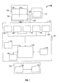
- FIG. 1 illustrates a block diagram of a monitoring system 100 according to some embodiments.
- the monitoring system 100 includes sensors 110, an imaging device 112, and a controller 114.
- the monitoring system 100 may be in wireless communication with factory automation infrastructure 116.
- the sensors 110 electronically communicate with the controller 114 through a first interconnect 120 and the imaging device 112 electronically communicates with the controller 114 through a second interconnect 122.
- the interconnects 120, 122 are insulated electrically conductive groups of wires.
- each sensor may have a separate wire in the interconnect 120 for separate communication with the controller 1 14.
- the sensors 110 and the imaging device 112 may communicate with the controller 114 in other ways, such as by wireless communication, without departing from the scope of the present disclosure.
- the sensors 110 are configured to be secured to a wafer handling machine used for semiconductor device fabrication, as will be described below.
- the sensors 110 in the example provided include level or tilt sensors 130, temperature sensors 132, vibration sensors 134, and harmonics sensors 136.
- the sensors 110 permit near real time scratch detection.
- the vibration sensors 134 may detect when a robot is vibrating and may cause scratching.
- the harmonics sensors 136 may be used to determine if the acoustics of the machine are changing over time, which may indicate a risk of misalignment and wafer scratches.
- the different sensors 130, 132, 134, 136 may be provided separately or may be packaged together in one sensor housing. In some embodiments, only the tilt sensors 130 are utilized.
- the sensors 110 are micro-electro-mechanical systems (MEMS) sensors.
- MEMS micro-electro-mechanical systems
- the sensors 110 generate output signals to the first interconnect 120 for analysis by the controller 114.
- a tilt sensor 130 may generate an analog voltage or current signal that indicates the orientation of the level sensor 130 with respect to Earth's gravitational pull. The magnitude of the generated signal may then be analyzed by the controller 114 to determine when the alignment of the wafer handling machine has changed.
- the imaging device 112 is configured to be secured to the wafer handling machine and capture images at the same portion of different handling cycles. For example, the imaging device 112 may capture an image of a robotic arm each time the arm enters a load port, as will be described below. The captured images may be analyzed by the controller 114 to determine when a height of a component of the wafer handling machine is out of alignment. For example, worm gears or ball screws may wear out and cause the vertical alignment of a robotic arm to vary from a reference height.
- the imaging device 112 is a charge-coupled device (CCD) camera.
- the imaging device 112 generates a signal on the second interconnect 122 to transfer digital images to the controller 114 for analysis. It should be appreciated that the imaging device 112 may transfer single images or may transfer substantially continuous video without departing from the scope of the present disclosure.
- the image comparing capabilities of the controller 114 (described below) are incorporated into the imaging device 112.
- the controller 114 receives signals generated by the sensors 110 and the imaging device 112 for analyzing changes in the alignment of the wafer handling machine.
- the controller 114 includes sensor inputs 140, an imaging device input 142, a power supply 144, control logic 146, a reference capture button 147, and a wireless modem 148.
- the sensor inputs 140 are electronically coupled to the sensors 110 to receive the output signals generated by the sensors 110.
- the sensor inputs 140 may receive analog outputs generated by the tilt sensors 130 that indicate a tilt angle of the tilt sensors 130.
- the imaging device input 142 is electronically coupled with the imaging device 112 to receive the images generated by the imaging device 112.
- the imaging device input 142 may receive digital images from the imaging device 112 that indicate a height of a robotic arm of the wafer handling machine.
- the control logic 146 may include any control circuitry capable of performing the various tasks described below.
- the control logic 146 may include an application specific integrated circuit (ASIC), an electronic circuit, a processor (shared, dedicated, or group) and memory that execute one or more software or firmware programs, a combinational logic circuit, and/or other suitable components that provide the described functionality.
- the control logic 146 may be hardware-based logic, or may include a combination of hardware, firmware, and/or software elements.
- the control logic 146 is configured to perform at least some of the operations described below with reference to FIG. 3 .
- the control logic 146 may capture and store reference outputs from the sensors 110 and the imaging device 112 when the reference capture button 147 is pressed.
- the control logic 146 further compares the output signals of the sensors 110 and imaging device 112 with the stored reference outputs. When a difference between the reference outputs and a current output generated by the sensors 110 exceeds a threshold, the control logic 146 generates in indication signal.
- Storing the reference outputs and comparing current values to the reference outputs reduces the need for costly calibration procedures where the sensors are configured to provide the level of the sensor with respect to the Z direction.
- the technician may manually align a column 222 and a load port 212 so that both the column 222 and the load port 212 are at the same slight angle with respect to the Z direction. Such an alignment does not lead to scratching of the wafer during handling and is therefore suitable for a stored reference output.
- the wireless modem 148 sends the indication signal to a wireless modem 150 in the infrastructure 116.
- the wireless modems 148, 150 may utilize any suitable wireless protocol.
- the wireless modems 148, 150 are replaced with wired network communications.
- the monitoring application 152 of the infrastructure 116 sends alerts and inhibits further wafer delivery to the wafer handling machine from which the indication signal originated.
- the monitoring application 152 may page, email, text, or otherwise alert a technician that the wafer handling machine should be serviced. Inhibiting further wafer delivery may include routing all continuing production to a different wafer handling machine or load port.
- the EFEM 200 is a wafer handling machine for loading semiconductor wafers into various processing equipment.
- the EFEM 200 may load wafers into processing tools for vacuum processing, metrology stages to take measurements on the wafer, wet sinks to wash off the wafer, etc.
- the monitoring system 100 may be incorporated on any equipment where wafers are handled (e.g., robots inside tools, processing chucks, etc.) without departing from the scope of the present disclosure.
- the EFEM 200 includes a robotic arm 210, a first load port 212, a second load port 214, a third load port 216, and an automation control module 218 for controlling movement of the robotic arm
- the robotic arm 210 includes a track 220, a column 222, and an end effector 224.
- the robotic arm 210 translates along an X axis on the track 220 to access each of the load ports 212, 214, 216.
- the column 222 compresses and expands to translate the end effector 224 along a Z axis.
- the column 222 also rotates to translate the end effector 224 along a Y axis.
- front opening unified pods (FOUPs) 230 are placed on the load ports 212, 214, 216.
- the FOUPs 230 each initially include stacked semiconductor wafers 232 and a door 234.
- the semiconductor wafers 232 may be, for example, slices of crystalline silicon in various stages of semiconductor fabrication processing.
- the door 234 may be opened by a mechanism in the load port on which the FOUP 230 is placed.
- the wafers 232 are spaced apart in the vertical direction to permit the end effector 224 to enter the FOUP 230 between the wafers 232 for removing the topmost wafer 232.
- the EFEM 200 components are aligned by a technician before use.
- the tilt sensors 130 may be secured to various components of the EFEM 200 to monitor the alignment of the components.
- the sensors 130 may be secured in any suitable fashion.
- the sensors 130 are secured to the EFEM 200 after final assembly of the EFEM 200. Accordingly, the sensors 130 are configured to be secured to any component of a variety of machines that may already be utilized in a factory.
- the tilt sensors 130 are secured to the outside of the components of the EFEM 200 using adhesive strips.
- the tilt sensors 130 are secured to the column 222, a base of the EFEM 200, and each of the load ports 212, 214, 216.
- the imaging device 112 is secured to the EFEM 200 adjacent to where the end effector 224 enters the load ports.
- the independence of the controller 114 from the automation control module 218 promotes use of the system 100 on various machines.
- the controller 1 14 is not limited by the type of software used by the manufacturer of the EFEM 200 to indicate misalignment.
- the system 100 is transported between different machines within a factory that each include different automation control modules.
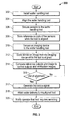
- a method 300 of monitoring wafer handling is presented in flow diagram form in accordance with some embodiments.
- a wafer handling tool is installed.
- the fully assembled EFEM 200 may be installed in a factory.
- the wafer handling machine has no built-in alignment sensing capability.
- the wafer handling tool is aligned. For example, a technician may manually level each component of the tool using levels or other equipment.
- Sensors are secured to the assembled wafer handling tool in operation 306.
- the technician may secure the sensors 110 to the EFEM 200 using adhesive strips.
- the sensors 110 may be secured to any component of the wafer handling tool.
- the tilt sensors 130 may be secured to the column 222, the base, and the load ports 212, 214, 216 of the EFEM 200.
- the modular nature and manufacturer independent nature of the system 100 promote retrofitting tools that are already used in production.
- reference outputs are captured and stored while the wafer handling machine is aligned.
- the technician may press the reference capture button 147 to indicate that the EFEM 200 is aligned.
- the controller 114 may then store the outputs generated by the sensors 110 at the time the button 147 was pressed.
- the output generated by the tilt sensors 130 corresponds to an angle of the tilt sensors 130, and therefore an angle of the column 122 or the load port 212, 214, 216.
- an imaging device is secured to the wafer handling tool.
- the imaging device 112 may be secured to the EFEM 200 adjacent to the load port 212.
- a reference image is captured and stored while the tool is aligned.
- the controller 114 may store the reference image at a portion of the handling cycle where the end effector 224 enters the load port 214.
- the reference outputs and the reference image are compared to current outputs from the sensors and verification images from the imaging device.
- the controller 114 may calculate a difference between the reference output of the sensors 110 and an output currently generated by the sensors 110.
- the controller 114 may compare the reference image stored in operation 312 with verification images captured each time the end effector 224 enters the load port 214 at the portion of a current handling cycle. Accordingly, the controller 114 is able to compare the current location of the end effector 224 to the taught reference location of the end effector 224 to determine if the end effector 224 is misaligned in the Z direction.
- Operation 316 determines whether the tool is out of alignment. For example, the controller 114 may determine the tool is out of alignment when a difference between one of the reference outputs and a current output of at least one of the sensors exceeds a threshold.
- the threshold for the tilt sensors 130 corresponds to a 0.1 degree variation from the aligned position.
- operation 314 is repeated to continuously monitor the alignment of the tool.
- an indication signal is generated in operation 317.
- the controller 114 may generate the indication signal and communicate the indication signal to the factory automation infrastructure 116 using the wireless modem 148.
- Wafer delivery to the misaligned tool is inhibited in operation 318.
- the control logic 146 of the controller 114 may instruct the factory automation infrastructure 116 to re-route further wafer delivery from the first load port 212 to the second and third load ports 214, 216 when the first load port 212 is misaligned.
- the infrastructure 116 re-routes further wafer delivery to different machines when the column 222 is out of alignment.
- an operator is notified that the tool requires servicing.
- the controller 114 or the infrastructure 116 may generate an email, a text, a page, or other notification for the technician. It should be appreciated that any suitable type of notification may be incorporated without departing from the scope of the present disclosure.
- Embodiments provided herein exhibit beneficial attributes for wafer handling monitoring. Scratches during wafer handling may be reduced by utilizing the modular monitoring system on existing machines.
- the modular nature of the system promotes portability and utilization on different machines through the life of the system. Storing reference levels while the machine is aligned reduces reliance on costly calibration services offered by tool manufacturers. Additionally, the systems and methods permit near real-time monitoring of tool alignment from a central location.
Landscapes
- Engineering & Computer Science (AREA)
- General Engineering & Computer Science (AREA)
- Manufacturing & Machinery (AREA)
- Quality & Reliability (AREA)
- Physics & Mathematics (AREA)
- General Physics & Mathematics (AREA)
- Automation & Control Theory (AREA)
- Container, Conveyance, Adherence, Positioning, Of Wafer (AREA)
- Testing And Monitoring For Control Systems (AREA)
- Robotics (AREA)
Abstract
Description
- The present disclosure relates to semiconductor wafer handling. More particularly, the present disclosure relates to monitoring machine alignment to detect potential scratches during semiconductor wafer handling.
- Manufacturing of integrated circuits and other microdevices involves a variety of process steps that are performed in various machines. A thin slice of semiconductor material (a wafer) is typically moved or handed off between the different machines using a robotic wafer handler. Components of the robotic wafer handler may become misaligned due to component wear or accidental human interference. For example, a 0.1 degree tilt on a component of the wafer handler may result in a robotic arm scratching the wafer during handling.
- Scratched wafers are typically discarded, resulting in lost tool time and materials. Furthermore, a typical wafer processing sequence may not detect the scratch until several process steps later when the wafer is examined. During the several process steps hundreds of wafers may have already been scratched by the misaligned tool.
- Additional steps may be added to check whether a tool is scratching. The additional steps are typically performed on a weekly basis using wafers and a defect tool. These steps cost cycle time and wafers, and may still result in undetected scratches for a period of time. During the period of scratching, thousands of wafers may be scratched. Increasing the frequency of the additional steps causes even more tool time to be lost.
- Accordingly, it is desirable to provide a system and method for monitoring wafer handling for potential wafer scratches. In addition, it is desirable to provide an improved wafer handling machine. Furthermore, other desirable features and characteristics will become apparent from the subsequent detailed description and the appended claims, taken in conjunction with the accompanying drawings, brief summary, and this background.
- Systems, machines, and methods for monitoring wafer handling are disclosed herein. In one embodiment, a system for monitoring wafer handling includes a sensor and a controller. The sensor is configured to be secured to an assembled wafer handling machine. The controller is in electronic communication with the sensor and includes control logic. The control logic is configured to store a reference output of the sensor when the wafer handling machine is aligned and is configured to generate an indication signal when a difference between the reference output and a current output of the sensor exceeds a threshold.
- In another exemplary embodiment, a wafer handling machine includes a load port, a robotic arm, a sensor, a controller, and an automation control module. The load port is capable of holding wafers and the robotic arm is capable of picking up and moving the wafers. The sensor is secured to an outside of at least one of the load port and the robotic arm. The controller includes control logic to store a reference output of the sensor when the wafer handling machine is aligned and to generate an indication signal when a difference between the reference output and a current output of the sensor exceeds a threshold. The automation control module is configured to control movement of the robotic arm and is separate from the controller.
- In another exemplary embodiment, a method of monitoring wafer handling is provided. The method includes storing a reference output of a sensor that is secured to a wafer handling machine when the wafer handling machine is aligned, and generating an indication signal when a difference between the reference output and a current output of the sensor exceeds a threshold.
- The method according to the invention may further comprise securing the sensor to a component of an assembled semiconductor wafer handling machine, wherein securing the sensor may further securing at least one of a tilt sensor, a vibration sensor, a temperature sensor, a vibration sensor, and a harmonics sensor. The method according to the invention may additionally comprise securing an imaging device to the assembled semiconductor wafer handling machine; storing a reference image from the imaging device when a wafer handling component of the wafer handling machine is at a reference height during a portion of a handling cycle; capturing a verification image from the imaging device during the portion of another handling cycle; and generating the indication signal when a difference between the reference image and the verification image indicates that a difference between the reference height and the height of the wafer handling component in the verification image exceeds a threshold. The method according to the invention may also comprise inhibiting automated delivery of semiconductor wafers to the wafer handling machine based on the indication signal, and/ or securing a tilt sensor to a robotic arm of the wafer handling machine and securing a tilt sensor to a load port of the wafer handling machine.
- Exemplary embodiments of the present disclosure will hereinafter be described in conjunction with the following drawing figures, wherein like numerals denote like elements, and wherein:
-
FIG. 1 is a block diagram of a monitoring system in accordance with some embodiments; -
FIG. 2A andFIG. 2B are isometric views of a wafer handling machine including the monitoring system ofFIG. 1 in accordance with some embodiments; and -
FIG. 3 is a flow diagram of a method for monitoring wafer handling in accordance with some embodiments. - The following detailed description is merely illustrative in nature and is not intended to limit the embodiments of the subject matter or the application and uses of such embodiments. As used herein, the word "exemplary" means "serving as an example, instance or illustration." Any implementation described herein as exemplary is not necessarily to be construed as preferred or advantageous over other implementations. Furthermore, there is no intention to be bound by any expressed or implied theory presented in the preceding Technical Field, Background, Brief Summary or the following Detailed Description
- The following description refers to elements or nodes or features being "connected or "coupled" together. As used herein, unless expressly stated otherwise, "coupled" means that one element/node/feature is directly joined to (or directly or indirectly communicates with) another element/node/feature, and not necessarily mechanically. Likewise, unless expressly stated otherwise, "connect" means that one element/node feature is directly joined to (or directly communicates with) another element/node/feature, and not necessarily mechanically.
- In general, embodiments provided herein utilize tilt sensors and displacement sensors to verify that frames of wafer tools, chambers, and loadports stay in alignment. Wafer scratching from misaligned tools may therefore be reduced. The system may be used with a wide variety of wafer handling machines that have different components and configurations.
-
FIG. 1 illustrates a block diagram of amonitoring system 100 according to some embodiments. Themonitoring system 100 includessensors 110, animaging device 112, and acontroller 114. Themonitoring system 100 may be in wireless communication withfactory automation infrastructure 116. Thesensors 110 electronically communicate with thecontroller 114 through afirst interconnect 120 and theimaging device 112 electronically communicates with thecontroller 114 through asecond interconnect 122. In the example provided, theinterconnects interconnect 120 for separate communication with the controller 1 14. It should be appreciated that thesensors 110 and theimaging device 112 may communicate with thecontroller 114 in other ways, such as by wireless communication, without departing from the scope of the present disclosure. - The
sensors 110 are configured to be secured to a wafer handling machine used for semiconductor device fabrication, as will be described below. Thesensors 110 in the example provided include level ortilt sensors 130,temperature sensors 132,vibration sensors 134, andharmonics sensors 136. Thesensors 110 permit near real time scratch detection. For example, thevibration sensors 134 may detect when a robot is vibrating and may cause scratching. Theharmonics sensors 136 may be used to determine if the acoustics of the machine are changing over time, which may indicate a risk of misalignment and wafer scratches. Thedifferent sensors tilt sensors 130 are utilized. - In some embodiments, the
sensors 110 are micro-electro-mechanical systems (MEMS) sensors. Thesensors 110 generate output signals to thefirst interconnect 120 for analysis by thecontroller 114. For example, atilt sensor 130 may generate an analog voltage or current signal that indicates the orientation of thelevel sensor 130 with respect to Earth's gravitational pull. The magnitude of the generated signal may then be analyzed by thecontroller 114 to determine when the alignment of the wafer handling machine has changed. - The
imaging device 112 is configured to be secured to the wafer handling machine and capture images at the same portion of different handling cycles. For example, theimaging device 112 may capture an image of a robotic arm each time the arm enters a load port, as will be described below. The captured images may be analyzed by thecontroller 114 to determine when a height of a component of the wafer handling machine is out of alignment. For example, worm gears or ball screws may wear out and cause the vertical alignment of a robotic arm to vary from a reference height. - In the example provided, the
imaging device 112 is a charge-coupled device (CCD) camera. Theimaging device 112 generates a signal on thesecond interconnect 122 to transfer digital images to thecontroller 114 for analysis. It should be appreciated that theimaging device 112 may transfer single images or may transfer substantially continuous video without departing from the scope of the present disclosure. In some embodiments, the image comparing capabilities of the controller 114 (described below) are incorporated into theimaging device 112. - The
controller 114 receives signals generated by thesensors 110 and theimaging device 112 for analyzing changes in the alignment of the wafer handling machine. Thecontroller 114 includessensor inputs 140, animaging device input 142, apower supply 144,control logic 146, areference capture button 147, and awireless modem 148. Thesensor inputs 140 are electronically coupled to thesensors 110 to receive the output signals generated by thesensors 110. For example, thesensor inputs 140 may receive analog outputs generated by thetilt sensors 130 that indicate a tilt angle of thetilt sensors 130. Theimaging device input 142 is electronically coupled with theimaging device 112 to receive the images generated by theimaging device 112. For example, theimaging device input 142 may receive digital images from theimaging device 112 that indicate a height of a robotic arm of the wafer handling machine. - The
control logic 146 may include any control circuitry capable of performing the various tasks described below. For example, thecontrol logic 146 may include an application specific integrated circuit (ASIC), an electronic circuit, a processor (shared, dedicated, or group) and memory that execute one or more software or firmware programs, a combinational logic circuit, and/or other suitable components that provide the described functionality. In some embodiments, thecontrol logic 146 may be hardware-based logic, or may include a combination of hardware, firmware, and/or software elements. - The
control logic 146 is configured to perform at least some of the operations described below with reference toFIG. 3 . For example, thecontrol logic 146 may capture and store reference outputs from thesensors 110 and theimaging device 112 when thereference capture button 147 is pressed. Thecontrol logic 146 further compares the output signals of thesensors 110 andimaging device 112 with the stored reference outputs. When a difference between the reference outputs and a current output generated by thesensors 110 exceeds a threshold, thecontrol logic 146 generates in indication signal. - Storing the reference outputs and comparing current values to the reference outputs reduces the need for costly calibration procedures where the sensors are configured to provide the level of the sensor with respect to the Z direction. For example, referring momentarily to
FIG. 2 , the technician may manually align acolumn 222 and aload port 212 so that both thecolumn 222 and theload port 212 are at the same slight angle with respect to the Z direction. Such an alignment does not lead to scratching of the wafer during handling and is therefore suitable for a stored reference output. - Referring back to
FIG. 1 , thewireless modem 148 sends the indication signal to awireless modem 150 in theinfrastructure 116. It should be appreciated that thewireless modems wireless modems - The
monitoring application 152 of theinfrastructure 116 sends alerts and inhibits further wafer delivery to the wafer handling machine from which the indication signal originated. For example, themonitoring application 152 may page, email, text, or otherwise alert a technician that the wafer handling machine should be serviced. Inhibiting further wafer delivery may include routing all continuing production to a different wafer handling machine or load port. - Referring now to
FIGS. 2A and2B , isometric views of an equipment front end module (EFEM) 200 incorporating themonitoring system 100 are illustrated in accordance with some embodiments. In general, theEFEM 200 is a wafer handling machine for loading semiconductor wafers into various processing equipment. For example, theEFEM 200 may load wafers into processing tools for vacuum processing, metrology stages to take measurements on the wafer, wet sinks to wash off the wafer, etc. It should be appreciated that themonitoring system 100 may be incorporated on any equipment where wafers are handled (e.g., robots inside tools, processing chucks, etc.) without departing from the scope of the present disclosure. - The
EFEM 200 includes arobotic arm 210, afirst load port 212, a second load port 214, athird load port 216, and anautomation control module 218 for controlling movement of the robotic arm Therobotic arm 210 includes atrack 220, acolumn 222, and anend effector 224. Therobotic arm 210 translates along an X axis on thetrack 220 to access each of theload ports column 222 compresses and expands to translate theend effector 224 along a Z axis. Thecolumn 222 also rotates to translate theend effector 224 along a Y axis. - During operation of the
EFEM 200, front opening unified pods (FOUPs) 230 are placed on theload ports FOUPs 230 each initially include stackedsemiconductor wafers 232 and adoor 234. Thesemiconductor wafers 232 may be, for example, slices of crystalline silicon in various stages of semiconductor fabrication processing. Thedoor 234 may be opened by a mechanism in the load port on which theFOUP 230 is placed. Thewafers 232 are spaced apart in the vertical direction to permit theend effector 224 to enter theFOUP 230 between thewafers 232 for removing thetopmost wafer 232. In order to prevent theend effector 224 from scratching the wafers, theEFEM 200 components are aligned by a technician before use. - The
tilt sensors 130 may be secured to various components of theEFEM 200 to monitor the alignment of the components. Thesensors 130 may be secured in any suitable fashion. In some embodiments, thesensors 130 are secured to theEFEM 200 after final assembly of theEFEM 200. Accordingly, thesensors 130 are configured to be secured to any component of a variety of machines that may already be utilized in a factory. In the example provided, thetilt sensors 130 are secured to the outside of the components of theEFEM 200 using adhesive strips. In the example provided, thetilt sensors 130 are secured to thecolumn 222, a base of theEFEM 200, and each of theload ports imaging device 112 is secured to theEFEM 200 adjacent to where theend effector 224 enters the load ports. - The independence of the
controller 114 from theautomation control module 218 promotes use of thesystem 100 on various machines. For example, the controller 1 14 is not limited by the type of software used by the manufacturer of theEFEM 200 to indicate misalignment. In some embodiments, thesystem 100 is transported between different machines within a factory that each include different automation control modules. - Referring now to
FIG. 3 , amethod 300 of monitoring wafer handling is presented in flow diagram form in accordance with some embodiments. In operation 302 a wafer handling tool is installed. For example, the fully assembledEFEM 200 may be installed in a factory. In the example provided, the wafer handling machine has no built-in alignment sensing capability. Inoperation 304 the wafer handling tool is aligned. For example, a technician may manually level each component of the tool using levels or other equipment. - Sensors are secured to the assembled wafer handling tool in
operation 306. For example, the technician may secure thesensors 110 to theEFEM 200 using adhesive strips. Thesensors 110 may be secured to any component of the wafer handling tool. For example, thetilt sensors 130 may be secured to thecolumn 222, the base, and theload ports EFEM 200. The modular nature and manufacturer independent nature of thesystem 100 promote retrofitting tools that are already used in production. - In
operation 308 reference outputs are captured and stored while the wafer handling machine is aligned. For example, the technician may press thereference capture button 147 to indicate that theEFEM 200 is aligned. Thecontroller 114 may then store the outputs generated by thesensors 110 at the time thebutton 147 was pressed. As previously described, the output generated by thetilt sensors 130 corresponds to an angle of thetilt sensors 130, and therefore an angle of thecolumn 122 or theload port - In
operation 310 an imaging device is secured to the wafer handling tool. For example, theimaging device 112 may be secured to theEFEM 200 adjacent to theload port 212. In operation 312 a reference image is captured and stored while the tool is aligned. For example, when thereference capture button 147 is pressed thecontroller 114 may store the reference image at a portion of the handling cycle where theend effector 224 enters the load port 214. - In
operation 314 the reference outputs and the reference image are compared to current outputs from the sensors and verification images from the imaging device. For example, thecontroller 114 may calculate a difference between the reference output of thesensors 110 and an output currently generated by thesensors 110. Similarly, thecontroller 114 may compare the reference image stored inoperation 312 with verification images captured each time theend effector 224 enters the load port 214 at the portion of a current handling cycle. Accordingly, thecontroller 114 is able to compare the current location of theend effector 224 to the taught reference location of theend effector 224 to determine if theend effector 224 is misaligned in the Z direction. -
Operation 316 determines whether the tool is out of alignment. For example, thecontroller 114 may determine the tool is out of alignment when a difference between one of the reference outputs and a current output of at least one of the sensors exceeds a threshold. In some embodiments, the threshold for thetilt sensors 130 corresponds to a 0.1 degree variation from the aligned position. - When the tool is not out of alignment,
operation 314 is repeated to continuously monitor the alignment of the tool. When the tool is out of alignment, an indication signal is generated inoperation 317. For example, thecontroller 114 may generate the indication signal and communicate the indication signal to thefactory automation infrastructure 116 using thewireless modem 148. - Wafer delivery to the misaligned tool is inhibited in
operation 318. For example, thecontrol logic 146 of thecontroller 114 may instruct thefactory automation infrastructure 116 to re-route further wafer delivery from thefirst load port 212 to the second andthird load ports 214, 216 when thefirst load port 212 is misaligned. In some embodiments, theinfrastructure 116 re-routes further wafer delivery to different machines when thecolumn 222 is out of alignment. - In
operation 320 an operator is notified that the tool requires servicing. For example, thecontroller 114 or theinfrastructure 116 may generate an email, a text, a page, or other notification for the technician. It should be appreciated that any suitable type of notification may be incorporated without departing from the scope of the present disclosure. - Embodiments provided herein exhibit beneficial attributes for wafer handling monitoring. Scratches during wafer handling may be reduced by utilizing the modular monitoring system on existing machines. The modular nature of the system promotes portability and utilization on different machines through the life of the system. Storing reference levels while the machine is aligned reduces reliance on costly calibration services offered by tool manufacturers. Additionally, the systems and methods permit near real-time monitoring of tool alignment from a central location.
- While at least one exemplary embodiment has been presented in the foregoing detailed description, it should be appreciated that a vast number of variations exist. It should also be appreciated that the exemplary embodiment or exemplary embodiments are only examples, and are not intended to limit the scope, applicability, or configuration of the invention in any way. Rather, the foregoing detailed description will provide those skilled in the art with a convenient road map for implementing the exemplary embodiment or exemplary embodiments. It should be understood that various changes can be made in the function and arrangement of elements without departing from the scope of the invention as set forth in the appended claims and the legal equivalents thereof.
Claims (15)
- A system for monitoring wafer handling, the system comprising:a sensor capable of being secured to an assembled wafer handling machine; anda controller in electronic communication with the sensor and including control logic to:store a reference output of the sensor when the wafer handling machine is aligned; andgenerate an indication signal when a difference between the reference output and a current output of the sensor exceeds a threshold.
- The system of claim 1 wherein the system includes a tilt sensor secured to an assembled wafer handling machine.
- The system of claim 2 wherein the sensor comprises a plurality of sensors including a vibration sensor, a temperature sensor, a vibration sensor, and a harmonics sensor.
- The system of claim 1 further comprising an imaging device, and wherein the controller further includes control logic to:store a reference image from the imaging device that indicates a reference height of a component of the wafer handling machine during a portion of a handling cycle;capture a verification image from the imaging device during the portion of another handling cycle; andgenerate the indication signal when a difference between the reference image and the verification image indicates that a difference between the reference height and the height of the wafer handling component in the verification image exceeds a threshold.
- The system of claim 1 wherein the controller further includes control logic to command inhibition of automated delivery of semiconductor wafers to the wafer handling machine based on the indication signal.
- The system of claim 1 wherein the controller further includes a wireless modem for communicating the indication signal.
- The system of claim 1 wherein the controller further includes a button, and wherein the control logic is further configured to store the reference output when the button is pressed.
- A wafer handling machine comprising:a load port capable of holding wafers;a robotic arm capable of picking up and moving the wafers;a sensor secured to an outside of at least one of the load port and the robotic arm;a controller including control logic to:store a reference output of the sensor when the wafer handling machine is aligned; andgenerate an indication signal when a difference between the reference output and a current output of the sensor exceeds a threshold; andan automation control module for controlling movement of the robotic arm, wherein the automation control module is separate from the controller.
- The wafer handling machine of claim 8 wherein the sensor includes a tilt sensor.
- The wafer handling machine of claim 8 wherein the sensor comprises a plurality of sensors including a vibration sensor, a temperature sensor, a vibration sensor, and a harmonics sensor.
- The wafer handling machine of claim 8 further comprising an imaging device, and wherein the controller further includes control logic to:store a reference image from the imaging device when the robotic arm is at a reference height during a portion of a handling cycle;capture a verification image from the imaging device during the portion of another handling cycle; andgenerate the indication signal when a difference between the reference image and the verification image indicates that a difference between the reference height and the height of the robotic arm in the verification image exceeds a threshold.
- The wafer handling machine of claim 8 wherein the controller further includes control logic command inhibition of automated delivery of semiconductor wafers to the wafer handling machine based on the indication signal.
- The wafer handling machine of claim 8 wherein the controller further includes a wireless modem for communicating the indication signal.
- The wafer handling machine of claim 8 wherein the controller further includes a button, and wherein the control logic is further configured to store the reference output when the button is pressed
- A method of monitoring wafer handling, the method comprising:storing a reference output of a sensor when a wafer handling machine is aligned, wherein the sensor is secured to the wafer handling machine; andgenerating an indication signal when a difference between the reference output and a current output of the sensor exceeds a threshold.
Priority Applications (1)
| Application Number | Priority Date | Filing Date | Title |
|---|---|---|---|
| EP17155850.5A EP3185282B1 (en) | 2013-04-29 | 2014-04-29 | A system and method for monitoring wafer handling and a wafer handling machine |
Applications Claiming Priority (1)
| Application Number | Priority Date | Filing Date | Title |
|---|---|---|---|
| US13/872,734 US9442482B2 (en) | 2013-04-29 | 2013-04-29 | System and method for monitoring wafer handling and a wafer handling machine |
Related Child Applications (2)
| Application Number | Title | Priority Date | Filing Date |
|---|---|---|---|
| EP17155850.5A Division EP3185282B1 (en) | 2013-04-29 | 2014-04-29 | A system and method for monitoring wafer handling and a wafer handling machine |
| EP17155850.5A Division-Into EP3185282B1 (en) | 2013-04-29 | 2014-04-29 | A system and method for monitoring wafer handling and a wafer handling machine |
Publications (2)
| Publication Number | Publication Date |
|---|---|
| EP2800132A1 true EP2800132A1 (en) | 2014-11-05 |
| EP2800132B1 EP2800132B1 (en) | 2017-06-28 |
Family
ID=50819545
Family Applications (2)
| Application Number | Title | Priority Date | Filing Date |
|---|---|---|---|
| EP14166341.9A Not-in-force EP2800132B1 (en) | 2013-04-29 | 2014-04-29 | A system and method for monitoring wafer handling and a wafer handling machine |
| EP17155850.5A Not-in-force EP3185282B1 (en) | 2013-04-29 | 2014-04-29 | A system and method for monitoring wafer handling and a wafer handling machine |
Family Applications After (1)
| Application Number | Title | Priority Date | Filing Date |
|---|---|---|---|
| EP17155850.5A Not-in-force EP3185282B1 (en) | 2013-04-29 | 2014-04-29 | A system and method for monitoring wafer handling and a wafer handling machine |
Country Status (7)
| Country | Link |
|---|---|
| US (2) | US9442482B2 (en) |
| EP (2) | EP2800132B1 (en) |
| JP (1) | JP6325325B2 (en) |
| KR (2) | KR20140128861A (en) |
| CN (1) | CN104124189B (en) |
| DE (1) | DE102014204945A1 (en) |
| TW (1) | TWI670154B (en) |
Families Citing this family (28)
| Publication number | Priority date | Publication date | Assignee | Title |
|---|---|---|---|---|
| US9442482B2 (en) * | 2013-04-29 | 2016-09-13 | GlobalFoundries, Inc. | System and method for monitoring wafer handling and a wafer handling machine |
| JP6607661B2 (en) * | 2013-08-09 | 2019-11-20 | 日本電産サンキョー株式会社 | Horizontal articulated robot |
| US10780586B2 (en) | 2013-08-09 | 2020-09-22 | Nidec Sankyo Corporation | Horizontal articulated robot with bevel gears |
| US20150185731A1 (en) * | 2013-12-26 | 2015-07-02 | Hyundai Motor Company | Work-in-process inspection system using motion detection, and method thereof |
| TWI639906B (en) * | 2017-06-16 | 2018-11-01 | 中原大學 | Active assembly system, active assembly method and positioning assembly device thereof |
| US10714364B2 (en) | 2017-08-31 | 2020-07-14 | Taiwan Semiconductor Manufacturing Co., Ltd. | Apparatus and method for inspecting wafer carriers |
| TWI693564B (en) * | 2018-01-05 | 2020-05-11 | 竹陞科技股份有限公司 | Automatic equipment management system and method thereof |
| US11247330B2 (en) * | 2018-10-19 | 2022-02-15 | Asm Ip Holding B.V. | Method for teaching a transportation position and alignment jig |
| US11094570B2 (en) * | 2019-03-29 | 2021-08-17 | Hirata Corporation | Load port having movable member that abuts a pin |
| JP7319162B2 (en) | 2019-10-02 | 2023-08-01 | 株式会社荏原製作所 | Transport abnormality prediction system |
| US12485554B2 (en) * | 2019-11-01 | 2025-12-02 | Lam Research Corporation | Wafer handling robot with gravitational field sensor |
| CN111430265B (en) * | 2019-11-28 | 2023-09-12 | 合肥晶合集成电路股份有限公司 | A device and method for blocking machine windows and semiconductor equipment |
| CN113013057B (en) * | 2019-12-20 | 2025-04-01 | 台湾积体电路制造股份有限公司 | System and method for processing wafers |
| CN111092039B (en) * | 2019-12-30 | 2022-04-15 | 武汉大学 | Wafer transmission system |
| CN111107324A (en) * | 2019-12-31 | 2020-05-05 | 上海陛通半导体能源科技股份有限公司 | Monitoring device and monitoring method of wafer transmission system |
| WO2021164667A1 (en) * | 2020-02-19 | 2021-08-26 | 宋茂炎 | Wafer, and calibration apparatus and calibration method for transfer mechanism of wafer |
| US11302545B2 (en) * | 2020-03-20 | 2022-04-12 | Nanya Technology Corporation | System and method for controlling semiconductor manufacturing equipment |
| CN111554601B (en) * | 2020-04-27 | 2021-12-28 | 上海果纳半导体技术有限公司 | Wafer front end transfer system |
| TWI777213B (en) | 2020-08-05 | 2022-09-11 | 華邦電子股份有限公司 | Transportation monitoring method and system thereof |
| CN114446844A (en) * | 2020-11-03 | 2022-05-06 | 长鑫存储技术有限公司 | Conveying device and semiconductor production equipment |
| JP7712077B2 (en) * | 2020-12-21 | 2025-07-23 | 株式会社ディスコ | Conveying mechanism and processing device |
| CN113031669B (en) * | 2021-02-10 | 2022-04-22 | 国机集团科学技术研究院有限公司 | High-quality crystal cultivation key process environment vibration control technical analysis method |
| CN112936217B (en) * | 2021-02-19 | 2025-03-11 | 深圳优艾智合机器人科技有限公司 | Wafer box handling robot |
| KR102820399B1 (en) | 2021-09-29 | 2025-06-12 | 삼성전자주식회사 | Equipment front end module and destructive analysis automation apparatus including the same |
| CN114084619B (en) * | 2021-11-24 | 2023-06-20 | 华中科技大学鄂州工业技术研究院 | A production line intelligent control system and method |
| US11728194B2 (en) * | 2021-12-07 | 2023-08-15 | Nanya Technology Corporation | Wafer handling apparatus and method of operating the same |
| KR102717235B1 (en) * | 2022-03-18 | 2024-10-15 | 주식회사 테스 | A substrate processing system |
| CN117125472A (en) * | 2023-10-11 | 2023-11-28 | 捷螺智能设备(苏州)有限公司 | A robot for transporting wafer cassettes that can be flexibly adjusted in multiple directions |
Citations (3)
| Publication number | Priority date | Publication date | Assignee | Title |
|---|---|---|---|---|
| EP0597637A1 (en) * | 1992-11-12 | 1994-05-18 | Applied Materials, Inc. | System and method for automated positioning of a substrate in a processing chamber |
| US20030202092A1 (en) * | 2002-04-19 | 2003-10-30 | Applied Materials, Inc. | Vision system |
| US20090062960A1 (en) * | 2007-08-30 | 2009-03-05 | Sekar Krishnasamy | Method and system for robot calibrations with a camera |
Family Cites Families (25)
| Publication number | Priority date | Publication date | Assignee | Title |
|---|---|---|---|---|
| JPH09232404A (en) * | 1996-02-19 | 1997-09-05 | Yaskawa Electric Corp | Wafer transfer device |
| JPH10313037A (en) | 1997-05-06 | 1998-11-24 | Applied Materials Inc | Monitoring system for substrate transfer system |
| US6466231B1 (en) | 1998-08-07 | 2002-10-15 | Hewlett-Packard Company | Appliance and method of using same for capturing images |
| JP2001082925A (en) | 1999-09-14 | 2001-03-30 | Sony Corp | Ultraviolet light focal position control mechanism and method, and inspection apparatus and method |
| JP3694808B2 (en) * | 2001-04-13 | 2005-09-14 | 株式会社安川電機 | Wafer transfer robot teaching method and teaching plate |
| US7085622B2 (en) * | 2002-04-19 | 2006-08-01 | Applied Material, Inc. | Vision system |
| US6813543B2 (en) * | 2002-10-08 | 2004-11-02 | Brooks-Pri Automation, Inc. | Substrate handling system for aligning and orienting substrates during a transfer operation |
| KR101015778B1 (en) * | 2003-06-03 | 2011-02-22 | 도쿄엘렉트론가부시키가이샤 | How to adjust the substrate processing apparatus and substrate delivery position |
| JP4342923B2 (en) * | 2003-12-09 | 2009-10-14 | 大日本スクリーン製造株式会社 | Substrate processing apparatus and substrate processing method |
| KR100577582B1 (en) * | 2004-06-09 | 2006-05-08 | 삼성전자주식회사 | Semiconductor photo spinner facility and wafer teaching defect prevention method using same |
| JP2006278396A (en) | 2005-03-28 | 2006-10-12 | Tokyo Electron Ltd | Processing apparatus and program |
| US20060215347A1 (en) | 2005-03-28 | 2006-09-28 | Tokyo Electron Limited | Processing apparatus and recording medium |
| CN101263499B (en) | 2005-07-11 | 2013-03-27 | 布鲁克斯自动化公司 | Intelligent condition monitoring and fault diagnostic system |
| US8014887B2 (en) * | 2006-03-22 | 2011-09-06 | Hitachi Kokusai Electric Inc. | Substrate processing apparatus |
| US8224607B2 (en) * | 2007-08-30 | 2012-07-17 | Applied Materials, Inc. | Method and apparatus for robot calibrations with a calibrating device |
| US9269529B2 (en) * | 2007-12-27 | 2016-02-23 | Lam Research Corporation | Systems and methods for dynamic alignment beam calibration |
| JP4382156B2 (en) * | 2008-02-12 | 2009-12-09 | パナソニック株式会社 | Compound eye imaging device, distance measuring device, parallax calculation method, and distance measuring method |
| JP2009229184A (en) | 2008-03-21 | 2009-10-08 | Kansai Electric Power Co Inc:The | Harmonic probing method and device |
| JP2009233788A (en) | 2008-03-27 | 2009-10-15 | Daihen Corp | Method of controlling carrier robot |
| US8624989B2 (en) | 2008-07-01 | 2014-01-07 | Sony Corporation | System and method for remotely performing image processing operations with a network server device |
| TWI496732B (en) * | 2009-07-31 | 2015-08-21 | 村田機械股份有限公司 | Buffer storage and transport device for tool utilization |
| JP5387444B2 (en) | 2010-02-25 | 2014-01-15 | 株式会社ニコン | Conveying apparatus and substrate bonding apparatus |
| JP2011192676A (en) | 2010-03-11 | 2011-09-29 | Nikon Corp | Substrate processing apparatus, method of manufacturing multilayer semiconductor device, and multilayer semiconductor device |
| JP5477133B2 (en) * | 2010-04-09 | 2014-04-23 | 日新イオン機器株式会社 | Wafer handling method and ion implantation apparatus |
| US9442482B2 (en) * | 2013-04-29 | 2016-09-13 | GlobalFoundries, Inc. | System and method for monitoring wafer handling and a wafer handling machine |
-
2013
- 2013-04-29 US US13/872,734 patent/US9442482B2/en active Active
- 2013-12-17 TW TW102146556A patent/TWI670154B/en active
-
2014
- 2014-03-07 KR KR1020140027372A patent/KR20140128861A/en not_active Ceased
- 2014-03-18 DE DE102014204945.8A patent/DE102014204945A1/en not_active Withdrawn
- 2014-04-17 JP JP2014085665A patent/JP6325325B2/en not_active Expired - Fee Related
- 2014-04-29 EP EP14166341.9A patent/EP2800132B1/en not_active Not-in-force
- 2014-04-29 EP EP17155850.5A patent/EP3185282B1/en not_active Not-in-force
- 2014-04-29 CN CN201410178064.0A patent/CN104124189B/en active Active
-
2016
- 2016-07-29 US US15/223,882 patent/US10593575B2/en active Active
-
2017
- 2017-06-14 KR KR1020170075038A patent/KR102128995B1/en active Active
Patent Citations (3)
| Publication number | Priority date | Publication date | Assignee | Title |
|---|---|---|---|---|
| EP0597637A1 (en) * | 1992-11-12 | 1994-05-18 | Applied Materials, Inc. | System and method for automated positioning of a substrate in a processing chamber |
| US20030202092A1 (en) * | 2002-04-19 | 2003-10-30 | Applied Materials, Inc. | Vision system |
| US20090062960A1 (en) * | 2007-08-30 | 2009-03-05 | Sekar Krishnasamy | Method and system for robot calibrations with a camera |
Also Published As
| Publication number | Publication date |
|---|---|
| US10593575B2 (en) | 2020-03-17 |
| US20140324208A1 (en) | 2014-10-30 |
| US9442482B2 (en) | 2016-09-13 |
| DE102014204945A1 (en) | 2014-11-13 |
| TWI670154B (en) | 2019-09-01 |
| KR20170072853A (en) | 2017-06-27 |
| EP3185282B1 (en) | 2018-08-29 |
| EP3185282A1 (en) | 2017-06-28 |
| EP2800132B1 (en) | 2017-06-28 |
| CN104124189A (en) | 2014-10-29 |
| KR20140128861A (en) | 2014-11-06 |
| US20160336206A1 (en) | 2016-11-17 |
| CN104124189B (en) | 2017-09-12 |
| TW201440980A (en) | 2014-11-01 |
| KR102128995B1 (en) | 2020-07-02 |
| JP6325325B2 (en) | 2018-05-16 |
| JP2014216648A (en) | 2014-11-17 |
Similar Documents
| Publication | Publication Date | Title |
|---|---|---|
| US10593575B2 (en) | System and method for monitoring wafer handling and a wafer handling machine | |
| US10020182B2 (en) | Digital wireless data collection | |
| US20190164790A1 (en) | Systems and methods for wafer pod calibration | |
| KR102020533B1 (en) | End effector detecting module and end effector monitoring device using the same | |
| KR102329653B1 (en) | Method for reducing eccentricity of substrate and teaching apparatus | |
| US12169179B2 (en) | Method and apparatus for monitoring edge bevel removal area in semiconductor apparatus and electroplating system | |
| JP2021525947A5 (en) | ||
| TW201925054A (en) | Systems and methods for automated material handing | |
| CN111107324A (en) | Monitoring device and monitoring method of wafer transmission system | |
| KR102380139B1 (en) | Semiconductor Fabricating Apparatus Having Member for Transferring Wafers And Method for Transferring Wafers Using The Same | |
| KR102723780B1 (en) | Inspection method, inspection device, and plating apparatus including the same | |
| CN111554594A (en) | Wafer transfer monitoring method and wafer transfer monitoring device | |
| JP2006310349A (en) | System and method of manufacturing semiconductor device | |
| KR102910429B1 (en) | Teaching system, method for transfer bobot and camera jig apparatus | |
| KR100780383B1 (en) | Semiconductor process equipment remote control system and method | |
| US12288703B2 (en) | Wafer process monitoring system and method | |
| CN224267239U (en) | Vision-based wafer transfer system | |
| KR20160148882A (en) | System for inspecting picker units | |
| KR20060025834A (en) | Detection system for detecting abnormality of semiconductor manufacturing apparatus and wafer during process and control method thereof | |
| TW202538912A (en) | Semiconductor processing method, transport case and semiconductor processing system | |
| KR20140037584A (en) | Semiconductor process equipment remote control system and method | |
| CN114078160A (en) | Transportation monitoring method and system thereof | |
| KR20250135085A (en) | Substrate processing system | |
| TW202514878A (en) | Method of monitoring substrate carrier apparatus and substrate processing apparatus | |
| KR20060061986A (en) | Semiconductor manufacturing equipment |
Legal Events
| Date | Code | Title | Description |
|---|---|---|---|
| PUAI | Public reference made under article 153(3) epc to a published international application that has entered the european phase |
Free format text: ORIGINAL CODE: 0009012 |
|
| 17P | Request for examination filed |
Effective date: 20140429 |
|
| AK | Designated contracting states |
Kind code of ref document: A1 Designated state(s): AL AT BE BG CH CY CZ DE DK EE ES FI FR GB GR HR HU IE IS IT LI LT LU LV MC MK MT NL NO PL PT RO RS SE SI SK SM TR |
|
| AX | Request for extension of the european patent |
Extension state: BA ME |
|
| RIN1 | Information on inventor provided before grant (corrected) |
Inventor name: FOSNIGHT, WILLIAM JOHN Inventor name: GALLAGHER, RYAN Inventor name: MINER, STEPHEN BRADLEY |
|
| R17P | Request for examination filed (corrected) |
Effective date: 20150420 |
|
| RBV | Designated contracting states (corrected) |
Designated state(s): AL AT BE BG CH CY CZ DE DK EE ES FI FR GB GR HR HU IE IS IT LI LT LU LV MC MK MT NL NO PL PT RO RS SE SI SK SM TR |
|
| 17Q | First examination report despatched |
Effective date: 20150518 |
|
| GRAP | Despatch of communication of intention to grant a patent |
Free format text: ORIGINAL CODE: EPIDOSNIGR1 |
|
| INTG | Intention to grant announced |
Effective date: 20160916 |
|
| GRAJ | Information related to disapproval of communication of intention to grant by the applicant or resumption of examination proceedings by the epo deleted |
Free format text: ORIGINAL CODE: EPIDOSDIGR1 |
|
| GRAP | Despatch of communication of intention to grant a patent |
Free format text: ORIGINAL CODE: EPIDOSNIGR1 |
|
| INTC | Intention to grant announced (deleted) | ||
| INTG | Intention to grant announced |
Effective date: 20170110 |
|
| GRAS | Grant fee paid |
Free format text: ORIGINAL CODE: EPIDOSNIGR3 |
|
| GRAA | (expected) grant |
Free format text: ORIGINAL CODE: 0009210 |
|
| AK | Designated contracting states |
Kind code of ref document: B1 Designated state(s): AL AT BE BG CH CY CZ DE DK EE ES FI FR GB GR HR HU IE IS IT LI LT LU LV MC MK MT NL NO PL PT RO RS SE SI SK SM TR |
|
| REG | Reference to a national code |
Ref country code: GB Ref legal event code: FG4D |
|
| REG | Reference to a national code |
Ref country code: CH Ref legal event code: EP |
|
| REG | Reference to a national code |
Ref country code: AT Ref legal event code: REF Ref document number: 905542 Country of ref document: AT Kind code of ref document: T Effective date: 20170715 |
|
| REG | Reference to a national code |
Ref country code: IE Ref legal event code: FG4D |
|
| REG | Reference to a national code |
Ref country code: DE Ref legal event code: R096 Ref document number: 602014011141 Country of ref document: DE |
|
| PG25 | Lapsed in a contracting state [announced via postgrant information from national office to epo] |
Ref country code: GR Free format text: LAPSE BECAUSE OF FAILURE TO SUBMIT A TRANSLATION OF THE DESCRIPTION OR TO PAY THE FEE WITHIN THE PRESCRIBED TIME-LIMIT Effective date: 20170929 Ref country code: HR Free format text: LAPSE BECAUSE OF FAILURE TO SUBMIT A TRANSLATION OF THE DESCRIPTION OR TO PAY THE FEE WITHIN THE PRESCRIBED TIME-LIMIT Effective date: 20170628 Ref country code: LT Free format text: LAPSE BECAUSE OF FAILURE TO SUBMIT A TRANSLATION OF THE DESCRIPTION OR TO PAY THE FEE WITHIN THE PRESCRIBED TIME-LIMIT Effective date: 20170628 Ref country code: FI Free format text: LAPSE BECAUSE OF FAILURE TO SUBMIT A TRANSLATION OF THE DESCRIPTION OR TO PAY THE FEE WITHIN THE PRESCRIBED TIME-LIMIT Effective date: 20170628 Ref country code: NO Free format text: LAPSE BECAUSE OF FAILURE TO SUBMIT A TRANSLATION OF THE DESCRIPTION OR TO PAY THE FEE WITHIN THE PRESCRIBED TIME-LIMIT Effective date: 20170928 |
|
| REG | Reference to a national code |
Ref country code: NL Ref legal event code: MP Effective date: 20170628 |
|
| REG | Reference to a national code |
Ref country code: LT Ref legal event code: MG4D |
|
| REG | Reference to a national code |
Ref country code: AT Ref legal event code: MK05 Ref document number: 905542 Country of ref document: AT Kind code of ref document: T Effective date: 20170628 |
|
| PG25 | Lapsed in a contracting state [announced via postgrant information from national office to epo] |
Ref country code: RS Free format text: LAPSE BECAUSE OF FAILURE TO SUBMIT A TRANSLATION OF THE DESCRIPTION OR TO PAY THE FEE WITHIN THE PRESCRIBED TIME-LIMIT Effective date: 20170628 Ref country code: LV Free format text: LAPSE BECAUSE OF FAILURE TO SUBMIT A TRANSLATION OF THE DESCRIPTION OR TO PAY THE FEE WITHIN THE PRESCRIBED TIME-LIMIT Effective date: 20170628 Ref country code: BG Free format text: LAPSE BECAUSE OF FAILURE TO SUBMIT A TRANSLATION OF THE DESCRIPTION OR TO PAY THE FEE WITHIN THE PRESCRIBED TIME-LIMIT Effective date: 20170928 Ref country code: NL Free format text: LAPSE BECAUSE OF FAILURE TO SUBMIT A TRANSLATION OF THE DESCRIPTION OR TO PAY THE FEE WITHIN THE PRESCRIBED TIME-LIMIT Effective date: 20170628 Ref country code: SE Free format text: LAPSE BECAUSE OF FAILURE TO SUBMIT A TRANSLATION OF THE DESCRIPTION OR TO PAY THE FEE WITHIN THE PRESCRIBED TIME-LIMIT Effective date: 20170628 |
|
| PG25 | Lapsed in a contracting state [announced via postgrant information from national office to epo] |
Ref country code: SK Free format text: LAPSE BECAUSE OF FAILURE TO SUBMIT A TRANSLATION OF THE DESCRIPTION OR TO PAY THE FEE WITHIN THE PRESCRIBED TIME-LIMIT Effective date: 20170628 Ref country code: RO Free format text: LAPSE BECAUSE OF FAILURE TO SUBMIT A TRANSLATION OF THE DESCRIPTION OR TO PAY THE FEE WITHIN THE PRESCRIBED TIME-LIMIT Effective date: 20170628 Ref country code: CZ Free format text: LAPSE BECAUSE OF FAILURE TO SUBMIT A TRANSLATION OF THE DESCRIPTION OR TO PAY THE FEE WITHIN THE PRESCRIBED TIME-LIMIT Effective date: 20170628 Ref country code: AT Free format text: LAPSE BECAUSE OF FAILURE TO SUBMIT A TRANSLATION OF THE DESCRIPTION OR TO PAY THE FEE WITHIN THE PRESCRIBED TIME-LIMIT Effective date: 20170628 Ref country code: EE Free format text: LAPSE BECAUSE OF FAILURE TO SUBMIT A TRANSLATION OF THE DESCRIPTION OR TO PAY THE FEE WITHIN THE PRESCRIBED TIME-LIMIT Effective date: 20170628 |
|
| PG25 | Lapsed in a contracting state [announced via postgrant information from national office to epo] |
Ref country code: ES Free format text: LAPSE BECAUSE OF FAILURE TO SUBMIT A TRANSLATION OF THE DESCRIPTION OR TO PAY THE FEE WITHIN THE PRESCRIBED TIME-LIMIT Effective date: 20170628 Ref country code: IT Free format text: LAPSE BECAUSE OF FAILURE TO SUBMIT A TRANSLATION OF THE DESCRIPTION OR TO PAY THE FEE WITHIN THE PRESCRIBED TIME-LIMIT Effective date: 20170628 Ref country code: IS Free format text: LAPSE BECAUSE OF FAILURE TO SUBMIT A TRANSLATION OF THE DESCRIPTION OR TO PAY THE FEE WITHIN THE PRESCRIBED TIME-LIMIT Effective date: 20171028 Ref country code: SM Free format text: LAPSE BECAUSE OF FAILURE TO SUBMIT A TRANSLATION OF THE DESCRIPTION OR TO PAY THE FEE WITHIN THE PRESCRIBED TIME-LIMIT Effective date: 20170628 Ref country code: PL Free format text: LAPSE BECAUSE OF FAILURE TO SUBMIT A TRANSLATION OF THE DESCRIPTION OR TO PAY THE FEE WITHIN THE PRESCRIBED TIME-LIMIT Effective date: 20170628 |
|
| REG | Reference to a national code |
Ref country code: DE Ref legal event code: R097 Ref document number: 602014011141 Country of ref document: DE |
|
| PG25 | Lapsed in a contracting state [announced via postgrant information from national office to epo] |
Ref country code: DK Free format text: LAPSE BECAUSE OF FAILURE TO SUBMIT A TRANSLATION OF THE DESCRIPTION OR TO PAY THE FEE WITHIN THE PRESCRIBED TIME-LIMIT Effective date: 20170628 |
|
| PLBE | No opposition filed within time limit |
Free format text: ORIGINAL CODE: 0009261 |
|
| STAA | Information on the status of an ep patent application or granted ep patent |
Free format text: STATUS: NO OPPOSITION FILED WITHIN TIME LIMIT |
|
| 26N | No opposition filed |
Effective date: 20180329 |
|
| PG25 | Lapsed in a contracting state [announced via postgrant information from national office to epo] |
Ref country code: SI Free format text: LAPSE BECAUSE OF FAILURE TO SUBMIT A TRANSLATION OF THE DESCRIPTION OR TO PAY THE FEE WITHIN THE PRESCRIBED TIME-LIMIT Effective date: 20170628 |
|
| REG | Reference to a national code |
Ref country code: FR Ref legal event code: PLFP Year of fee payment: 5 |
|
| PG25 | Lapsed in a contracting state [announced via postgrant information from national office to epo] |
Ref country code: MC Free format text: LAPSE BECAUSE OF FAILURE TO SUBMIT A TRANSLATION OF THE DESCRIPTION OR TO PAY THE FEE WITHIN THE PRESCRIBED TIME-LIMIT Effective date: 20170628 |
|
| REG | Reference to a national code |
Ref country code: CH Ref legal event code: PL |
|
| REG | Reference to a national code |
Ref country code: BE Ref legal event code: MM Effective date: 20180430 |
|
| GBPC | Gb: european patent ceased through non-payment of renewal fee |
Effective date: 20180429 |
|
| REG | Reference to a national code |
Ref country code: IE Ref legal event code: MM4A |
|
| PG25 | Lapsed in a contracting state [announced via postgrant information from national office to epo] |
Ref country code: LU Free format text: LAPSE BECAUSE OF NON-PAYMENT OF DUE FEES Effective date: 20180429 |
|
| PG25 | Lapsed in a contracting state [announced via postgrant information from national office to epo] |
Ref country code: LI Free format text: LAPSE BECAUSE OF NON-PAYMENT OF DUE FEES Effective date: 20180430 Ref country code: GB Free format text: LAPSE BECAUSE OF NON-PAYMENT OF DUE FEES Effective date: 20180429 Ref country code: CH Free format text: LAPSE BECAUSE OF NON-PAYMENT OF DUE FEES Effective date: 20180430 Ref country code: BE Free format text: LAPSE BECAUSE OF NON-PAYMENT OF DUE FEES Effective date: 20180430 |
|
| PG25 | Lapsed in a contracting state [announced via postgrant information from national office to epo] |
Ref country code: IE Free format text: LAPSE BECAUSE OF NON-PAYMENT OF DUE FEES Effective date: 20180429 |
|
| PG25 | Lapsed in a contracting state [announced via postgrant information from national office to epo] |
Ref country code: MT Free format text: LAPSE BECAUSE OF NON-PAYMENT OF DUE FEES Effective date: 20180429 |
|
| PG25 | Lapsed in a contracting state [announced via postgrant information from national office to epo] |
Ref country code: TR Free format text: LAPSE BECAUSE OF FAILURE TO SUBMIT A TRANSLATION OF THE DESCRIPTION OR TO PAY THE FEE WITHIN THE PRESCRIBED TIME-LIMIT Effective date: 20170628 |
|
| PG25 | Lapsed in a contracting state [announced via postgrant information from national office to epo] |
Ref country code: PT Free format text: LAPSE BECAUSE OF FAILURE TO SUBMIT A TRANSLATION OF THE DESCRIPTION OR TO PAY THE FEE WITHIN THE PRESCRIBED TIME-LIMIT Effective date: 20170628 Ref country code: HU Free format text: LAPSE BECAUSE OF FAILURE TO SUBMIT A TRANSLATION OF THE DESCRIPTION OR TO PAY THE FEE WITHIN THE PRESCRIBED TIME-LIMIT; INVALID AB INITIO Effective date: 20140429 |
|
| PG25 | Lapsed in a contracting state [announced via postgrant information from national office to epo] |
Ref country code: CY Free format text: LAPSE BECAUSE OF FAILURE TO SUBMIT A TRANSLATION OF THE DESCRIPTION OR TO PAY THE FEE WITHIN THE PRESCRIBED TIME-LIMIT Effective date: 20170628 Ref country code: MK Free format text: LAPSE BECAUSE OF NON-PAYMENT OF DUE FEES Effective date: 20170628 |
|
| PG25 | Lapsed in a contracting state [announced via postgrant information from national office to epo] |
Ref country code: AL Free format text: LAPSE BECAUSE OF FAILURE TO SUBMIT A TRANSLATION OF THE DESCRIPTION OR TO PAY THE FEE WITHIN THE PRESCRIBED TIME-LIMIT Effective date: 20170628 |
|
| REG | Reference to a national code |
Ref country code: DE Ref legal event code: R082 Ref document number: 602014011141 Country of ref document: DE Representative=s name: GRUENECKER PATENT- UND RECHTSANWAELTE PARTG MB, DE Ref country code: DE Ref legal event code: R081 Ref document number: 602014011141 Country of ref document: DE Owner name: GLOBALFOUNDRIES U.S. INC., SANTA CLARA, US Free format text: FORMER OWNER: GLOBALFOUNDRIES INC., GRAND CAYMAN, KY |
|
| PGFP | Annual fee paid to national office [announced via postgrant information from national office to epo] |
Ref country code: FR Payment date: 20230309 Year of fee payment: 10 |
|
| P01 | Opt-out of the competence of the unified patent court (upc) registered |
Effective date: 20230412 |
|
| PGFP | Annual fee paid to national office [announced via postgrant information from national office to epo] |
Ref country code: DE Payment date: 20230307 Year of fee payment: 10 |
|
| REG | Reference to a national code |
Ref country code: DE Ref legal event code: R119 Ref document number: 602014011141 Country of ref document: DE |
|
| PG25 | Lapsed in a contracting state [announced via postgrant information from national office to epo] |
Ref country code: DE Free format text: LAPSE BECAUSE OF NON-PAYMENT OF DUE FEES Effective date: 20241105 |
|
| PG25 | Lapsed in a contracting state [announced via postgrant information from national office to epo] |
Ref country code: FR Free format text: LAPSE BECAUSE OF NON-PAYMENT OF DUE FEES Effective date: 20240430 |
|
| PG25 | Lapsed in a contracting state [announced via postgrant information from national office to epo] |
Ref country code: FR Free format text: LAPSE BECAUSE OF NON-PAYMENT OF DUE FEES Effective date: 20240430 Ref country code: DE Free format text: LAPSE BECAUSE OF NON-PAYMENT OF DUE FEES Effective date: 20241105 |