JP2011192676A - Substrate processing apparatus, method of manufacturing multilayer semiconductor device, and multilayer semiconductor device - Google Patents
Substrate processing apparatus, method of manufacturing multilayer semiconductor device, and multilayer semiconductor device Download PDFInfo
- Publication number
- JP2011192676A JP2011192676A JP2010055062A JP2010055062A JP2011192676A JP 2011192676 A JP2011192676 A JP 2011192676A JP 2010055062 A JP2010055062 A JP 2010055062A JP 2010055062 A JP2010055062 A JP 2010055062A JP 2011192676 A JP2011192676 A JP 2011192676A
- Authority
- JP
- Japan
- Prior art keywords
- substrate
- transfer arm
- processing apparatus
- substrate processing
- transfer
- Prior art date
- Legal status (The legal status is an assumption and is not a legal conclusion. Google has not performed a legal analysis and makes no representation as to the accuracy of the status listed.)
- Pending
Links
Images


Abstract
Description
本発明は、基板処理装置、積層半導体装置製造方法及び積層半導体装置に関する。 The present invention relates to a substrate processing apparatus, a stacked semiconductor device manufacturing method, and a stacked semiconductor device.
基板を処理する過程において、多くの工程でロボットの搬送アームにより基板を搬送する(特許文献1を参照)。
[先行技術文献]
[特許文献]
[特許文献1] 特開2010−10628号公報
In the process of processing a substrate, the substrate is transferred by a transfer arm of a robot in many steps (see Patent Document 1).
[Prior art documents]
[Patent Literature]
[Patent Document 1] Japanese Patent Application Laid-Open No. 2010-10628
ロボット搬送アームは、基板等を載置するときに、基板等の重量により許容範囲において撓むが、ベアリングの磨耗等により撓みが大きくなり、許容範囲を超えることがある。この場合に、そのまま搬送アームによる搬送を継続すると、搬送アーム又は搬送される基板等がチャンバー又は基板載置部等に接触して破損するおそれがある。 When placing a substrate or the like, the robot transfer arm bends within an allowable range due to the weight of the substrate or the like, but the deflection may increase due to wear of a bearing or the like, and may exceed the allowable range. In this case, if the transfer by the transfer arm is continued as it is, there is a risk that the transfer arm or the substrate to be transferred will come into contact with the chamber or the substrate mounting portion and be damaged.
上記課題を解決するために、基板を処理する複数の処理室に連結された連結室と、連結室に配され、基板を複数の処理室の間で搬送する搬送アームと、搬送アームを目標位置に移動した場合の搬送アームの実際の位置を計測する計測部と、目標位置と計測部により計測された位置との差を算出する算出部とを備える基板処理装置が提供される。 In order to solve the above problems, a connection chamber connected to a plurality of processing chambers for processing a substrate, a transfer arm arranged in the connection chamber for transferring a substrate between the plurality of processing chambers, and a transfer arm at a target position A substrate processing apparatus is provided that includes a measurement unit that measures the actual position of the transfer arm when moved to the position, and a calculation unit that calculates the difference between the target position and the position measured by the measurement unit.
本発明の第2の態様においては、上記基板処理装置により基板を処理することを含む積層半導体装置製造方法が提供される。 In a second aspect of the present invention, there is provided a method for manufacturing a laminated semiconductor device including processing a substrate by the substrate processing apparatus.
本発明の第3の態様においては、上記積層半導体装置製造方法により製造された積層半導体装置が提供される。 In a third aspect of the present invention, a stacked semiconductor device manufactured by the above-described stacked semiconductor device manufacturing method is provided.
なお、上記の発明の概要は、本発明の必要な特徴の全てを列挙したものではない。また、これらの特徴群のサブコンビネーションもまた、発明となりうる。 It should be noted that the above summary of the invention does not enumerate all the necessary features of the present invention. In addition, a sub-combination of these feature groups can also be an invention.
以下、発明の実施の形態を通じて本発明を説明するが、以下の実施形態は特許請求の範囲にかかる発明を限定するものではない。また、実施形態の中で説明されている特徴の組み合わせの全てが発明の解決手段に必須であるとは限らない。 Hereinafter, the present invention will be described through embodiments of the invention, but the following embodiments do not limit the invention according to the claims. In addition, not all the combinations of features described in the embodiments are essential for the solving means of the invention.
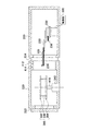
図1は、一の実施形態である基板貼り合せ装置100の全体構造を模式的に示す平面図である。基板貼り合せ装置100は、筐体102と、常温部104と、高温部106と、基板カセット112、114、116とを備える。常温部104および高温部106は、共通の筐体102の内部に設けられる。基板貼り合せ装置100は、基板処理装置の一例である。
FIG. 1 is a plan view schematically showing the overall structure of a
基板カセット112、114、116は、筐体102の外部に、筐体102に対して脱着自在に装着される。基板カセット112、114、116は、基板貼り合せ装置100において接合される第1基板122および第2基板123を収容する。基板カセット112、114、116により、複数の第1基板122および第2基板123が一括して基板貼り合せ装置100に装填される。また、基板貼り合せ装置100において接合された第1基板122および第2基板123が一括して回収される。
The
常温部104は、筐体102の内側にそれぞれ配された、プリアライナ126、ステージ装置140、基板ホルダラック128および基板取り外し部130と、一対の搬送アーム132、134とを備える。筐体102の内部は、基板貼り合せ装置100が設置された環境の室温と略同じ温度が維持されるように温度管理される。
The
プリアライナ126は、高精度であるが故にステージ装置140の狭い調整範囲に第1基板122または第2基板123の位置が収まるように、個々の第1基板122または第2基板123の位置を仮合わせする。これにより、ステージ装置140が確実に位置決めをすることができる。
Since the pre-aligner 126 is highly accurate, the position of each
基板ホルダラック128は、複数の上基板ホルダ124および複数の下基板ホルダ125を収容して待機させる。基板ホルダラック128は、基板取り外し部130の下方に配される。
The
ステージ装置140は、貼り合わせの対象である第1基板122と第2基板123における接合すべき電極同士の位置を合わせて、重ね合わせる。ステージ装置140は、上ステージ141と、下ステージ142と、制御部148とを含む。また、ステージ装置140を包囲して断熱壁145およびシャッタ146が設けられる。断熱壁145およびシャッタ146に包囲された空間は空調機等に連通して温度管理され、ステージ装置140における位置合わせ精度を維持する。
The
上ステージ141は、ステージ装置140の天板の下面に固定される。上ステージ141は、下向きの載置面において、真空吸着により上基板ホルダ124を吸着する。当該吸着方法は、静電吸着であってもよい。上基板ホルダ124は、その下面に静電吸着により第1基板122を吸着して保持する。
The
下ステージ142は、ステージ装置140の底板に設けられた移動ステージに配され、平行移動、上下移動及び傾斜移動ができる。下ステージ142は、上ステージ141に対向して、上向きの載置面を有し、それに真空吸着等により下基板ホルダ125を保持する。下基板ホルダ125は、静電吸着により第2基板123を保持する。
The
制御部148は、下ステージ142の移動を制御する。制御部148は、下ステージ142を移動させて、上ステージ141に保持された第1基板122に対して、第2基板123の位置を合わせる。制御部148は、下ステージ142を上昇させて、第1基板122と第2基板123を重ね合せることができる。その後、上基板ホルダ124と下基板ホルダ125に挟まれた第1基板122と第2基板123は、位置固定部材により仮止めされる。上基板ホルダ124と下基板ホルダ125及びそれらに挟まれた第1基板122と第2基板123はホルダ対120を形成する。
The
基板取り外し部130は、高温部106から搬出された上基板ホルダ124および下基板ホルダ125に挟まれて貼り合わされた第1基板122および第2基板123を取り出す。貼り合わされた第1基板122および第2基板123を「積層基板」と記載することがある。上基板ホルダ124および下基板ホルダ125から取り出された積層基板は、搬送アーム134、132および下ステージ142により基板カセット112、114、116のうちのひとつに戻されて収容される。積層基板を取り出された上基板ホルダ124および下基板ホルダ125は、基板ホルダラック128に戻されて待機する。基板取り外し部130は、基板ホルダラック128の上方に配される。
The
なお、基板貼り合せ装置100に装填される第1基板122および第2基板123は、単体のシリコンウエハ、化合物半導体ウェハ、ガラス基板等の他、それらに素子、回路、端子等が形成されたものであってよい。また、装填された第1基板122および第2基板123が、既に複数のウェハを積層して形成された積層基板である場合もある。
The
一対の搬送アーム132、134のうち、基板カセット112、114、116に近い側に配置された搬送アーム132は、基板カセット112、114、116、プリアライナ126およびステージ装置140の間で第1基板122および第2基板123を搬送する。一方、基板カセット112、114、116から遠い側に配置された搬送アーム134は、ステージ装置140、基板ホルダラック128、基板取り外し部130およびロードロック室220の間で、第1基板122、第2基板123、上基板ホルダ124および下基板ホルダ125を搬送する。
Of the pair of
搬送アーム134は、基板ホルダラック128に対して、上基板ホルダ124および下基板ホルダ125の搬入および搬出も担う。上ステージ141に第1基板122を保持させる場合に、搬送アーム134は、まず基板ホルダラック128から一枚の上基板ホルダ124を取り出して下ステージ142に載置する。下ステージ142は、基板カセット112、114、116に近い側に移動する。搬送アーム132は、プリアライナ126からプリアライメントされた第1基板122を取り出して、下ステージ142の上の上基板ホルダ124に載置して、静電吸着させる。
The
下ステージ142は、再び基板カセット112、114、116から遠い側に移動する。搬送アーム134は、下ステージ142から第1基板122を静電吸着した上基板ホルダ124を受け取り、裏返して上ステージ141に近づける。上ステージ141は、真空吸着によりその上基板ホルダ124を保持する。
The
搬送アーム134は、下ステージ142に下基板ホルダ125を載置する。搬送アーム132は、その上に第2基板123を載置して保持させる。これにより、下ステージ142に保持された第2基板123における回路等が形成された面は、上ステージ141に保持された第1基板122における回路等が形成された面に、対向するように配置される。
The
高温部106は、断熱壁108と、ロードロック室220と、複数の加圧室240と、その複数の加圧室240及びロードロック室220に連結された連結室250と、搬送アーム230と、搬送アーム232とを有する。断熱壁108は、高温部106を包囲して、高温部106の高い内部温度を維持すると共に、高温部106の外部への熱輻射を遮断する。これにより、高温部106の熱が常温部104に及ぼす影響を抑制する。高温部106は、その内部が一定の真空状態に維持される。これにより、高温部106に搬入された基板の汚染及び酸化を抑えることができる。
The
搬送アーム230および搬送アーム232は、連結室250に配される。搬送アーム230および搬送アーム232は、加圧室240のいずれかとロードロック室220との間でホルダ対120を搬送する。ロードロック室220は、常温部104側と高温部106側とに、交互に開閉するシャッタ222、224を有する。ロードロック室220は、常温部104と高温部106との間にホルダ対120を受け渡す過程において、ホルダ対120を仮置きする。
The
第1基板122、第2基板123、上基板ホルダ124および下基板ホルダ125から構成されるホルダ対120が常温部104から高温部106に搬入される場合、まず、常温部104側のシャッタ222が開かれ、搬送アーム134がホルダ対120をロードロック室220に搬入する。次に、常温部104側のシャッタ222が閉じられ、ロードロック室220内部が真空に引かれる。ロードロック室220内部の真空度が、高温部106側の真空度になったら、高温部106側のシャッタ224が開かれる。
When the
続いて、搬送アーム230および搬送アーム232のいずれかが、ロードロック室220からホルダ対120を搬出して、加圧室240のいずれかに装入する。加圧室240は、上基板ホルダ124と下基板ホルダ125に挟まれた状態で加圧室240に搬入された第1基板122及び第2基板123を加熱および加圧する。これにより第1基板122と第2基板123が接合されて、貼り合わされる。なお、加圧室240は、第1基板122及び第2基板123を加熱せずに加圧することで第1基板122及び第2基板123を貼り合わせてもよい。
Subsequently, either the
高温部106から常温部104にホルダ対120を搬出する場合は、上記の一連の動作を逆順で実行する。これらの一連の動作により、高温部106の内部雰囲気を常温部104側に漏らすことなく、ホルダ対120を高温部106に搬入または搬出できる。
When carrying out the
このように、基板貼り合せ装置100内の多くの領域において、上基板ホルダ124が第1基板122を保持した状態で、又は下基板ホルダ125が第2基板123を保持した状態で、搬送アーム134、230、232および下ステージ142により搬送される。第1基板122を保持した上基板ホルダ124又は第2基板123を保持した下基板ホルダ125が搬送される場合、搬送アーム134、230、232は、真空吸着、静電吸着等により上基板ホルダ124又は下基板ホルダ125を吸着して保持する。また、上基板ホルダ124又は下基板ホルダ125は、静電吸着により第1基板122または第2基板123を吸着して保持する。
Thus, in many areas in the
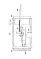
図2は、搬送アームの垂直方向の変形を計測する過程を概略に示す。図2は、ロードロック室220及び連結室250の側面断面を示す。ロードロック室220は、基板載置部300と、昇降機構342と、センサー412とを含む。
FIG. 2 schematically shows a process of measuring the vertical deformation of the transfer arm. FIG. 2 is a side cross-sectional view of the
基板載置部300は、上置き台302と、下置き台304と、接続柱306とを有する。上置き台302及び下置き台304は、上下平行に配置され、接続柱306により連結される。下置き台304は、ロードロック室220の下部に設置された昇降機構342に連結される。その連結により、基板載置部300の全体は、昇降機構342の駆動により上下に移動できる。
The
上置き台302及び下置き台304は、それぞれホルダ対120を載置することができる。例えば、上置き台302は、常温部104から搬入されるホルダ対120を載置し、下置き台304は、高温部106から搬入されるホルダ対120を載置する。
Each of the upper table 302 and the lower table 304 can mount the
昇降機構342は、基板載置部300を上下に駆動する。昇降機構342は、その内部にセンサー416が設けられ、基板載置部300にかかる負荷及びその変化を検出することができる。センサー416は、計測部の一例である。センサー416として、ロードセルが例示できる。センサー416により計測したデータは、搬送アームの制御部330に送信される。
The
センサー412は、搬送アーム230、232を予め定められた目標位置に移動した場合、垂直方向における搬送アーム230、232の実際の位置を計測する。ここで、「目標位置」とは、X、Y及びZ軸の座標が予め定められた位置を言う。センサー412は、計測部の一例である。センサー412により計測したデータは、搬送アームの制御部330に送信される。
The
センサー412として、レーザーセンサー等が例示できる。例えば、センサー412は、レーザーセンサーであって、ガラス窓414を越して、予め定められた目標位置に延伸した搬送アーム230のフィンガー234の先端にレーザービームを当てて、センサー412からフィンガー234の先端までの距離を計測することにより、搬送アーム230の垂直方向の位置を計測することができる。
An example of the
センサー412は、剛性の高いロードロック室220の筐体の上部に設けられるので、ロードロック室220の構造的不安定による計測誤差を回避できる。センサー412は、剛性の高いロードロック室220の筐体の底部に設けられてもよい。センサー412は、連結室250に配されてもよい。センサー412は、予め定められた距離まで搬送アーム230又は搬送アーム232が延伸した状態で、搬送アーム230又は搬送アーム232の垂直方向の変形を計測できる位置に配されて良い。
Since the
連結室250は、搬送アーム230、232を収容する。搬送アーム230、232は、搬送するホルダ対120の面に垂直な方向に重なって配置される。搬送アーム230、232は、互いに独立して動作する。センサー412又はセンサー416が搬送アーム230、232の一方の位置を計測する場合に、搬送アーム230、232はホルダ対120の面方向について互いにずれた位置にある。
The
搬送アーム230は、その先端にフィンガー234を有して、そのフィンガー234によって基板又はホルダ対120を保持する。搬送アーム232も、同様に、その先端にフィンガー236を有する。図2は、搬送アーム230が延伸して、搬送アーム232が退避した状態を示す。
The
基板貼り合せ装置100は、搬送アーム230、232を制御する制御部330を有する。制御部330は、センサー412及びセンサー416から受信した計測データに基づいて、搬送アーム230、232を制御する。制御部330は、センサー412及びセンサー416から受信した計測データに基づいて、搬送アーム230、232の実際の位置を算出することができる。制御部330は、算出部の一例でもある。
The
図3は、搬送アーム230の垂直方向の変形を概略的に説明する図面である。例えば、搬送アーム230が上置き台302との間にホルダ対120を受け渡す高さでは、フィンガー234がホルダ対120を保持しなければ、フィンガー234と上置き台302との間隔をHとする。上置き台302には、ホルダ対120に静電吸着の電力を供給する給電端子346があり、その高さをhとする。また、搬送アーム230がホルダ対120を保持し、更に磨耗等により垂直方向に生じる総変形をδとする。この場合に、ベアリングの磨耗等により、総変形δが(H−h)を超えると、フィンガー234は、給電端子346に、極端の場合には上置き台302に衝突して破損するおそれがある。
FIG. 3 is a diagram schematically illustrating the vertical deformation of the
例えば、H=8mm、h=1.5mmである場合に、総変形δが(H−h)=6.5mmを超えてはならない。搬送アーム230が4kgのホルダ対120を保持して、1235mmまで延伸したときに、搬送アーム230の撓みδ0が6mmである場合に、フィンガー234と給電端子346の頂点との間に残った間隔は0.5mmだけである。
For example, when H = 8 mm and h = 1.5 mm, the total deformation δ should not exceed (H−h) = 6.5 mm. When the
図2に示す実施形態において、制御部330は、ホルダ対120を保持した状態で搬送アーム230を予め定められた目標位置に移動する。センサー412は、搬送アーム230の垂直方向における実際の位置を計測する。制御部330は、上記目標位置とセンサー412により計測された位置との差を算出し、その差が閾値を超えたら搬送アーム230の動作を停止して、警告を発する。上記目標位置と計測位置との差は、図3に示すδである。例えば、閾値を6.3mmに設定して、δ>6.3mmになると、制御部330は、搬送アーム230の動作を停止して、警告を発する。これにより、搬送アーム230の破損事故を未然に防ぐことができる。なお当該警告は、基板貼り合せ装置100の使用者に、上記差が閾値を超えたことを認識させるものであって、LEDの点灯、操作画面への表示、音声の出力等を含む。さらに、当該警告は、基板貼り合せ装置100に連結された他の装置への情報の出力であってもよい。
In the embodiment shown in FIG. 2, the controller 330 moves the
図4は、計測ポイントの例を示す。制御部330が搬送アーム230を予め定められた目標位置に移動してから、センサー412は、フィンガー234の先端であるA又はBを測定ポイントとして、搬送アーム230の垂直方向における実際の位置を計測してよい。なお、ロードロック室220及び連結室250に複数のセンサーを設けて、A、B及びCのいずれか2ポイントを計測してもよく、A、B及びCの3点を計測してもよく、更に測定ポイントを増やして計測しても良い。
FIG. 4 shows an example of measurement points. After the controller 330 moves the
例えば、A、B及びCの3点が計測され、その計測データが制御部330に送信されると、制御部330は、そのデータに基づいて、搬送アーム230の傾きを計算することができる。従って、制御部330に傾きの閾値が設定されておけば、垂直な方向における搬送アーム230の傾きがその閾値を超えたら、制御部330は、搬送アーム230の動作を停止して、警告を発することができる。
For example, when three points A, B, and C are measured and the measurement data is transmitted to the control unit 330, the control unit 330 can calculate the inclination of the
上記の実施形態では、搬送アーム230がホルダ対120を保持した状態における搬送アーム230の垂直方向の実際位置を計測する例を挙げたが、ホルダ対120の代わりに、搬送アーム230がホルダ対120の質量に相当する対象物を保持した状態で計測してもよい。例えば、搬送アーム230がホルダ対120を保持すると、フィンガー234の先端が塞がれて、センサー412が直接フィンガー234の先端の位置を計測できないとき、搬送アーム230がホルダ対120と同じ質量を有し、ホルダ対120より一回り小さいダミー基板を保持した状態で計測が行われてもよい。
In the above-described embodiment, an example in which the actual position in the vertical direction of the
なお、搬送アーム230が既知の厚さを有するダミー基板を保持して、センサー412は、そのダミー基板までの間隔を計測して、計測データに基づいて制御部330が搬送アーム230の位置を算出してもよい。また、センサー412は、搬送アーム230がホルダ対120等を保持しない状態で、搬送アーム230を予め定められた目標位置に移動した場合の、垂直な方向における搬送アーム230の実際の位置を計測してもよい。この場合、搬送アーム230がホルダ対120等を保持しない状態に対応して、閾値が定められ、制御部330に設定されてもよい。
The
図5は、基板載置部を利用して搬送アームの垂直方向の変形を計測する実施形態を示す。制御部330は、ホルダ対120を保持した状態で搬送アーム230を予め定められた目標位置に、例えばフィンガー234の先端が下置き台304との間に垂直方向に予め定められた間隔を有すべき位置に移動する。昇降機構342は、基板載置部300を徐々に上昇させる。下置き台304がフィンガー234の先端に接触すると、センサー416は、基板載置部300にかかる負荷の変化を検出することができる。制御部330は、その検出データに基づいて、フィンガー234の実際の位置を算出することができる。
FIG. 5 shows an embodiment in which the vertical deformation of the transfer arm is measured using the substrate platform. The control unit 330 holds the
また、昇降機構342の内部に設けられたエンコーダを計測部として用いてもよい。この場合に、下置き台304がフィンガー234の先端に接触すると、昇降機構342のエンコーダは、目標プロファイルに対して非線形の検出データを出力する。従って、エンコーダの検出データを利用してもフィンガー234の実際の位置を検出することができる。
Further, an encoder provided in the
制御部330は、上記目標位置とセンサー416により計測された搬送アーム230の実際の位置との差を算出し、その差が閾値を超えたら搬送アーム230の動作を停止して、警告を発する。閾値は、上述の方法によって設定してよい。
The controller 330 calculates the difference between the target position and the actual position of the
図5に示す実施形態において、搬送アーム230は、ホルダ対120の代わりに、それと同じ質量を有するダミー基板を保持してもよく、基板等を保持しなくてもよい。搬送アーム230が基板等を保持しないときには、それに対応する閾値が定められてよい。制御部330は、上記目標位置とセンサー416により計測された搬送アーム230の実際の位置との差を算出し、その差が当該閾値を超えたら搬送アーム230の動作を停止して、警告を発してよい。
In the embodiment shown in FIG. 5, the
上述の実施形態において、主に搬送アーム230の例を挙げたが、搬送アーム232についても同様の計測をすることができる。また、定期的に搬送アーム230又は搬送アーム232の変形を計測することにより、搬送アーム230又は搬送アーム232の保守時期、例えばベアリングの交換時期を予測して、機械の破損事故を未然に防ぐことができる。上記予測は、定期的に搬送アーム230又は搬送アーム232の変形を計測することにより、予め定められた変形量となる時期を計測値から外挿して予測することであってよい。
In the above-described embodiment, the example of the
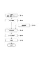
図6は、積層半導体装置を製造する製造方法の概略を示す。図6に示すように、積層半導体装置は、当該積層半導体装置の機能・性能設計を行うステップS110、この設計ステップに基づいたマスク(レチクル)を製作するステップS120、積層半導体装置の基材である基板を製造するステップS130、マスクのパターンを用いたリソグラフィを含む基板処理ステップS140、上記の基板貼り合せ装置を用いた基板貼り合せ工程等を含むデバイス組み立てステップS150、検査ステップS160等を経て製造される。なお、デバイス組み立てステップS150は、基板貼り合せ工程に続いて、ダイシング工程、ボンディング工程、パッケージ工程などの加工プロセスを含む。 FIG. 6 shows an outline of a manufacturing method for manufacturing a stacked semiconductor device. As shown in FIG. 6, the laminated semiconductor device is a base material for the laminated semiconductor device, step S110 for designing the function / performance of the laminated semiconductor device, step S120 for producing a mask (reticle) based on this design step, and step S120. It is manufactured through step S130 for manufacturing a substrate, substrate processing step S140 including lithography using a mask pattern, device assembly step S150 including a substrate bonding step using the above-described substrate bonding apparatus, inspection step S160, and the like. The The device assembly step S150 includes processing processes such as a dicing process, a bonding process, and a package process following the substrate bonding process.
以上、本発明を実施の形態を用いて説明したが、本発明の技術的範囲は上記実施の形態に記載の範囲には限定されない。上記実施の形態に、多様な変更又は改良を加えることができることが当業者に明らかである。その様な変更又は改良を加えた形態も本発明の技術的範囲に含まれ得ることが、特許請求の範囲の記載から明らかである。 As mentioned above, although this invention was demonstrated using embodiment, the technical scope of this invention is not limited to the range as described in the said embodiment. It will be apparent to those skilled in the art that various modifications or improvements can be added to the above-described embodiment. It is apparent from the description of the scope of claims that embodiments with such changes or improvements can be included in the technical scope of the present invention.
特許請求の範囲、明細書、及び図面中において示した装置、システム、プログラム、及び方法における動作、手順、ステップ、及び段階等の各処理の実行順序は、特段「より前に」、「先立って」等と明示しておらず、また、前の処理の出力を後の処理で用いるのでない限り、任意の順序で実現しうることに留意すべきである。特許請求の範囲、明細書、及び図面中の動作フローに関して、便宜上「まず、」、「次に、」等を用いて説明したとしても、この順で実施することが必須であることを意味するものではない。 The execution order of each process such as operation, procedure, step, and stage in the apparatus, system, program, and method shown in the claims, the description, and the drawings is particularly “before” or “prior to”. It should be noted that the output can be realized in any order unless the output of the previous process is used in the subsequent process. Regarding the operation flow in the claims, the specification, and the drawings, even if it is described using “first”, “next”, etc. for the sake of convenience, it means that it is essential to carry out in this order. It is not a thing.
100 基板貼り合せ装置、102 筐体、104 常温部、106 高温部、108 断熱壁、112 基板カセット、114 基板カセット、116 基板カセット、120 ホルダ対、122 第1基板、123 第2基板、124 上基板ホルダ、125 下基板ホルダ、126 プリアライナ、128 基板ホルダラック、130 基板取り外し部、132 搬送アーム、134 搬送アーム、140 ステージ装置、141 上ステージ、142 下ステージ、145 断熱壁、146 シャッタ、148 制御部、220 ロードロック室、222 シャッタ、224 シャッタ、230 搬送アーム、232 搬送アーム、234 フィンガー、236 フィンガー、240 加圧室、250 連結室、300 基板載置部、302 上置き台、304 下置き台、306 接続柱、330 制御部、342 昇降機構、346 給電端子、412 センサー、414 ガラス窓、416 センサー
DESCRIPTION OF
Claims (11)
前記連結室に配され、前記基板を前記複数の処理室の間で搬送する搬送アームと、
前記搬送アームを目標位置に移動した場合の前記搬送アームの実際の位置を計測する計測部と、
前記目標位置と前記計測部により計測された位置との差を算出する算出部と
を備える基板処理装置。 A connecting chamber connected to a plurality of processing chambers for processing a substrate;
A transfer arm arranged in the connection chamber and transferring the substrate between the plurality of processing chambers;
A measuring unit that measures the actual position of the transfer arm when the transfer arm is moved to a target position;
A substrate processing apparatus comprising: a calculation unit that calculates a difference between the target position and a position measured by the measurement unit.
前記複数の処理室の少なくとも他の一つは、前記搬送アームに受け渡す前記基板を仮置きするロードロック室である請求項1に記載の基板処理装置。 At least one of the plurality of processing chambers is a pressure chamber that presses and bonds the plurality of substrates in a reduced pressure environment,
The substrate processing apparatus according to claim 1, wherein at least another of the plurality of processing chambers is a load lock chamber for temporarily placing the substrate to be transferred to the transfer arm.
前記警告部は、前記搬送アームの傾きが閾値を超えたら警告する請求項6に記載の基板処理装置。 The measurement unit measures the transfer arm at a plurality of positions,
The substrate processing apparatus according to claim 6, wherein the warning unit warns when the inclination of the transfer arm exceeds a threshold value.
二つの前記搬送アームは互いに独立して動作し、
前記計測部が二つの前記搬送アームの一方の位置を計測する場合に、二つの前記搬送アームは前記基板の面方向について互いにずれた位置にある請求項1から8のいずれかに記載の基板処理装置。 Two transfer arms are arranged in a direction perpendicular to the surface of the substrate,
The two transfer arms operate independently of each other;
9. The substrate processing according to claim 1, wherein when the measurement unit measures one position of the two transfer arms, the two transfer arms are in positions shifted from each other in the plane direction of the substrate. apparatus.
Priority Applications (1)
| Application Number | Priority Date | Filing Date | Title |
|---|---|---|---|
| JP2010055062A JP2011192676A (en) | 2010-03-11 | 2010-03-11 | Substrate processing apparatus, method of manufacturing multilayer semiconductor device, and multilayer semiconductor device |
Applications Claiming Priority (1)
| Application Number | Priority Date | Filing Date | Title |
|---|---|---|---|
| JP2010055062A JP2011192676A (en) | 2010-03-11 | 2010-03-11 | Substrate processing apparatus, method of manufacturing multilayer semiconductor device, and multilayer semiconductor device |
Publications (2)
| Publication Number | Publication Date |
|---|---|
| JP2011192676A true JP2011192676A (en) | 2011-09-29 |
| JP2011192676A5 JP2011192676A5 (en) | 2013-06-27 |
Family
ID=44797321
Family Applications (1)
| Application Number | Title | Priority Date | Filing Date |
|---|---|---|---|
| JP2010055062A Pending JP2011192676A (en) | 2010-03-11 | 2010-03-11 | Substrate processing apparatus, method of manufacturing multilayer semiconductor device, and multilayer semiconductor device |
Country Status (1)
| Country | Link |
|---|---|
| JP (1) | JP2011192676A (en) |
Cited By (5)
| Publication number | Priority date | Publication date | Assignee | Title |
|---|---|---|---|---|
| CN102829722A (en) * | 2012-08-29 | 2012-12-19 | 江苏建威电子科技有限公司 | Position sensor |
| WO2016103292A1 (en) * | 2014-12-22 | 2016-06-30 | 川崎重工業株式会社 | Robot system and end-effector deformation detection method |
| CN106935538A (en) * | 2015-12-30 | 2017-07-07 | 上海微电子装备有限公司 | A kind of slide glass transmitting device and its transmission method |
| KR20190050274A (en) * | 2017-11-02 | 2019-05-10 | 조재용 | Robot sensing device for wafer transfer |
| US10593575B2 (en) | 2013-04-29 | 2020-03-17 | GlobalFoundries, Inc. | System and method for monitoring wafer handling and a wafer handling machine |
Citations (9)
| Publication number | Priority date | Publication date | Assignee | Title |
|---|---|---|---|---|
| JPH10275753A (en) * | 1997-03-31 | 1998-10-13 | Hitachi Ltd | Manufacture of semiconductor substrate |
| JP2001127136A (en) * | 1999-10-29 | 2001-05-11 | Applied Materials Inc | Inspection device for substrate transport robot |
| JP2005051171A (en) * | 2003-07-31 | 2005-02-24 | Applied Materials Inc | Substrate processing device |
| JP2006508526A (en) * | 2002-07-17 | 2006-03-09 | エムアールエル インダストリーズ | Heating element status monitor |
| JP2007281249A (en) * | 2006-04-07 | 2007-10-25 | Yaskawa Electric Corp | Conveyance robot and position correcting method thereof |
| JPWO2005024915A1 (en) * | 2003-09-02 | 2007-11-08 | 株式会社ニコン | Maintenance management apparatus, maintenance management method, maintenance management program, and information recording medium |
| JP2009123722A (en) * | 2007-11-12 | 2009-06-04 | Dainippon Screen Mfg Co Ltd | Substrate carrier |
| JP2009233788A (en) * | 2008-03-27 | 2009-10-15 | Daihen Corp | Method of controlling carrier robot |
| JP2010010628A (en) * | 2008-06-30 | 2010-01-14 | Nikon Corp | Bonding apparatus and bonding method |
-
2010
- 2010-03-11 JP JP2010055062A patent/JP2011192676A/en active Pending
Patent Citations (9)
| Publication number | Priority date | Publication date | Assignee | Title |
|---|---|---|---|---|
| JPH10275753A (en) * | 1997-03-31 | 1998-10-13 | Hitachi Ltd | Manufacture of semiconductor substrate |
| JP2001127136A (en) * | 1999-10-29 | 2001-05-11 | Applied Materials Inc | Inspection device for substrate transport robot |
| JP2006508526A (en) * | 2002-07-17 | 2006-03-09 | エムアールエル インダストリーズ | Heating element status monitor |
| JP2005051171A (en) * | 2003-07-31 | 2005-02-24 | Applied Materials Inc | Substrate processing device |
| JPWO2005024915A1 (en) * | 2003-09-02 | 2007-11-08 | 株式会社ニコン | Maintenance management apparatus, maintenance management method, maintenance management program, and information recording medium |
| JP2007281249A (en) * | 2006-04-07 | 2007-10-25 | Yaskawa Electric Corp | Conveyance robot and position correcting method thereof |
| JP2009123722A (en) * | 2007-11-12 | 2009-06-04 | Dainippon Screen Mfg Co Ltd | Substrate carrier |
| JP2009233788A (en) * | 2008-03-27 | 2009-10-15 | Daihen Corp | Method of controlling carrier robot |
| JP2010010628A (en) * | 2008-06-30 | 2010-01-14 | Nikon Corp | Bonding apparatus and bonding method |
Cited By (7)
| Publication number | Priority date | Publication date | Assignee | Title |
|---|---|---|---|---|
| CN102829722A (en) * | 2012-08-29 | 2012-12-19 | 江苏建威电子科技有限公司 | Position sensor |
| US10593575B2 (en) | 2013-04-29 | 2020-03-17 | GlobalFoundries, Inc. | System and method for monitoring wafer handling and a wafer handling machine |
| WO2016103292A1 (en) * | 2014-12-22 | 2016-06-30 | 川崎重工業株式会社 | Robot system and end-effector deformation detection method |
| CN106935538A (en) * | 2015-12-30 | 2017-07-07 | 上海微电子装备有限公司 | A kind of slide glass transmitting device and its transmission method |
| CN106935538B (en) * | 2015-12-30 | 2020-08-04 | 上海微电子装备(集团)股份有限公司 | Slide glass conveying device and conveying method thereof |
| KR20190050274A (en) * | 2017-11-02 | 2019-05-10 | 조재용 | Robot sensing device for wafer transfer |
| KR102022804B1 (en) * | 2017-11-02 | 2019-09-18 | 조재용 | Robot sensing device for wafer transfer |
Similar Documents
| Publication | Publication Date | Title |
|---|---|---|
| JP6423660B2 (en) | Method for determining pressure setting value for inspection in wafer inspection apparatus | |
| JP7420185B2 (en) | Board bonding equipment and board bonding method | |
| TWI743614B (en) | Substrate processing device and substrate processing method | |
| JP2011192676A (en) | Substrate processing apparatus, method of manufacturing multilayer semiconductor device, and multilayer semiconductor device | |
| KR20190075949A (en) | Joining device, joining system, joining method and computer storage medium | |
| JP2011049450A (en) | Alignment device, substrate bonding device, and method of manufacturing multilayer semiconductor device | |
| JP5549339B2 (en) | Substrate relative position detection method, laminated device manufacturing method, and detection apparatus | |
| JP2010045071A (en) | Detecting device, substrate holding member, transfer device, and bonding device | |
| JP2011216788A (en) | Substrate bonding apparatus and method of bonding substrate | |
| JP2013008804A (en) | Substrate bonding device, substrate bonding method, and method of manufacturing bonded semiconductor device | |
| TW202127512A (en) | Substrate bonding device and method | |
| JP5707793B2 (en) | Substrate bonding apparatus, substrate bonding method, and laminated semiconductor device manufacturing method | |
| KR101394312B1 (en) | Wafer alignment apparatus | |
| JP5386217B2 (en) | Display panel transfer device and display panel module assembly device | |
| JP2011151073A (en) | Bonding device and bonding method | |
| JP5585689B2 (en) | Substrate holder and bonding apparatus | |
| JP5798721B2 (en) | Substrate alignment apparatus, substrate bonding apparatus, substrate alignment method, and laminated semiconductor manufacturing method | |
| JP5454252B2 (en) | Substrate bonding apparatus, substrate bonding method, laminated semiconductor device manufacturing method, and laminated semiconductor device | |
| JP5454239B2 (en) | Substrate bonding apparatus, substrate bonding method, laminated semiconductor device manufacturing method, and laminated semiconductor device | |
| JP5560590B2 (en) | Substrate bonding equipment | |
| CN112342519A (en) | Film forming system, method for determining abnormal portion of film forming system, and computer-readable storage medium | |
| JP5724182B2 (en) | Substrate processing apparatus and laminated semiconductor device manufacturing method | |
| JP5614081B2 (en) | Substrate alignment device, substrate alignment method, substrate bonding device, laminated semiconductor device manufacturing method, and laminated semiconductor device | |
| JP2010093203A (en) | Reference mark moving apparatus and substrate alignment apparatus | |
| JP2012248733A (en) | Charged particle beam device and electrostatic chuck device |
Legal Events
| Date | Code | Title | Description |
|---|---|---|---|
| A621 | Written request for application examination |
Free format text: JAPANESE INTERMEDIATE CODE: A621 Effective date: 20130308 |
|
| A521 | Written amendment |
Free format text: JAPANESE INTERMEDIATE CODE: A523 Effective date: 20130510 |
|
| A977 | Report on retrieval |
Free format text: JAPANESE INTERMEDIATE CODE: A971007 Effective date: 20140220 |
|
| A131 | Notification of reasons for refusal |
Free format text: JAPANESE INTERMEDIATE CODE: A131 Effective date: 20140225 |
|
| A521 | Written amendment |
Free format text: JAPANESE INTERMEDIATE CODE: A523 Effective date: 20140423 |
|
| A131 | Notification of reasons for refusal |
Free format text: JAPANESE INTERMEDIATE CODE: A131 Effective date: 20140909 |
|
| A02 | Decision of refusal |
Free format text: JAPANESE INTERMEDIATE CODE: A02 Effective date: 20150203 |