EP2789092B1 - Turn-off overvoltage limiting for igbt - Google Patents
Turn-off overvoltage limiting for igbt Download PDFInfo
- Publication number
- EP2789092B1 EP2789092B1 EP12856190.9A EP12856190A EP2789092B1 EP 2789092 B1 EP2789092 B1 EP 2789092B1 EP 12856190 A EP12856190 A EP 12856190A EP 2789092 B1 EP2789092 B1 EP 2789092B1
- Authority
- EP
- European Patent Office
- Prior art keywords
- igbt
- emitter
- overvoltage
- gate driver
- collector
- Prior art date
- Legal status (The legal status is an assumption and is not a legal conclusion. Google has not performed a legal analysis and makes no representation as to the accuracy of the status listed.)
- Active
Links
Images


Classifications
-
- H—ELECTRICITY
- H02—GENERATION; CONVERSION OR DISTRIBUTION OF ELECTRIC POWER
- H02M—APPARATUS FOR CONVERSION BETWEEN AC AND AC, BETWEEN AC AND DC, OR BETWEEN DC AND DC, AND FOR USE WITH MAINS OR SIMILAR POWER SUPPLY SYSTEMS; CONVERSION OF DC OR AC INPUT POWER INTO SURGE OUTPUT POWER; CONTROL OR REGULATION THEREOF
- H02M7/00—Conversion of AC power input into DC power output; Conversion of DC power input into AC power output
- H02M7/42—Conversion of DC power input into AC power output without possibility of reversal
- H02M7/44—Conversion of DC power input into AC power output without possibility of reversal by static converters
- H02M7/48—Conversion of DC power input into AC power output without possibility of reversal by static converters using discharge tubes with control electrode or semiconductor devices with control electrode
- H02M7/53—Conversion of DC power input into AC power output without possibility of reversal by static converters using discharge tubes with control electrode or semiconductor devices with control electrode using devices of a triode or transistor type requiring continuous application of a control signal
- H02M7/537—Conversion of DC power input into AC power output without possibility of reversal by static converters using discharge tubes with control electrode or semiconductor devices with control electrode using devices of a triode or transistor type requiring continuous application of a control signal using semiconductor devices only, e.g. single switched pulse inverters
-
- H—ELECTRICITY
- H02—GENERATION; CONVERSION OR DISTRIBUTION OF ELECTRIC POWER
- H02M—APPARATUS FOR CONVERSION BETWEEN AC AND AC, BETWEEN AC AND DC, OR BETWEEN DC AND DC, AND FOR USE WITH MAINS OR SIMILAR POWER SUPPLY SYSTEMS; CONVERSION OF DC OR AC INPUT POWER INTO SURGE OUTPUT POWER; CONTROL OR REGULATION THEREOF
- H02M1/00—Details of apparatus for conversion
- H02M1/08—Circuits specially adapted for the generation of control voltages for semiconductor devices incorporated in static converters
-
- H—ELECTRICITY
- H02—GENERATION; CONVERSION OR DISTRIBUTION OF ELECTRIC POWER
- H02M—APPARATUS FOR CONVERSION BETWEEN AC AND AC, BETWEEN AC AND DC, OR BETWEEN DC AND DC, AND FOR USE WITH MAINS OR SIMILAR POWER SUPPLY SYSTEMS; CONVERSION OF DC OR AC INPUT POWER INTO SURGE OUTPUT POWER; CONTROL OR REGULATION THEREOF
- H02M1/00—Details of apparatus for conversion
- H02M1/32—Means for protecting converters other than automatic disconnection
-
- H—ELECTRICITY
- H03—ELECTRONIC CIRCUITRY
- H03K—PULSE TECHNIQUE
- H03K17/00—Electronic switching or gating, i.e. not by contact-making and –breaking
- H03K17/08—Modifications for protecting switching circuit against overcurrent or overvoltage
- H03K17/082—Modifications for protecting switching circuit against overcurrent or overvoltage by feedback from the output to the control circuit
- H03K17/0828—Modifications for protecting switching circuit against overcurrent or overvoltage by feedback from the output to the control circuit in composite switches
-
- H—ELECTRICITY
- H03—ELECTRONIC CIRCUITRY
- H03K—PULSE TECHNIQUE
- H03K17/00—Electronic switching or gating, i.e. not by contact-making and –breaking
- H03K17/16—Modifications for eliminating interference voltages or currents
- H03K17/161—Modifications for eliminating interference voltages or currents in field-effect transistor switches
- H03K17/165—Modifications for eliminating interference voltages or currents in field-effect transistor switches by feedback from the output circuit to the control circuit
- H03K17/166—Soft switching
-
- H—ELECTRICITY
- H03—ELECTRONIC CIRCUITRY
- H03K—PULSE TECHNIQUE
- H03K17/00—Electronic switching or gating, i.e. not by contact-making and –breaking
- H03K17/51—Electronic switching or gating, i.e. not by contact-making and –breaking characterised by the components used
- H03K17/56—Electronic switching or gating, i.e. not by contact-making and –breaking characterised by the components used by the use, as active elements, of semiconductor devices
- H03K17/60—Electronic switching or gating, i.e. not by contact-making and –breaking characterised by the components used by the use, as active elements, of semiconductor devices the devices being bipolar transistors
-
- H—ELECTRICITY
- H02—GENERATION; CONVERSION OR DISTRIBUTION OF ELECTRIC POWER
- H02M—APPARATUS FOR CONVERSION BETWEEN AC AND AC, BETWEEN AC AND DC, OR BETWEEN DC AND DC, AND FOR USE WITH MAINS OR SIMILAR POWER SUPPLY SYSTEMS; CONVERSION OF DC OR AC INPUT POWER INTO SURGE OUTPUT POWER; CONTROL OR REGULATION THEREOF
- H02M1/00—Details of apparatus for conversion
- H02M1/0003—Details of control, feedback or regulation circuits
- H02M1/0029—Circuits or arrangements for limiting the slope of switching signals, e.g. slew rate
-
- H—ELECTRICITY
- H10—SEMICONDUCTOR DEVICES; ELECTRIC SOLID-STATE DEVICES NOT OTHERWISE PROVIDED FOR
- H10W—GENERIC PACKAGES, INTERCONNECTIONS, CONNECTORS OR OTHER CONSTRUCTIONAL DETAILS OF DEVICES COVERED BY CLASS H10
- H10W72/00—Interconnections or connectors in packages
- H10W72/50—Bond wires
- H10W72/541—Dispositions of bond wires
- H10W72/547—Dispositions of multiple bond wires
- H10W72/5475—Dispositions of multiple bond wires multiple bond wires connected to common bond pads at both ends of the wires
Definitions
- the present disclosure generally relates to insulated gate bipolar transistors (IGBT). More specifically, the present disclosure is concerned with a configuration to limit the turn-off overvoltage on the IGBTs to thereby improve their overall efficiency.
- IGBT insulated gate bipolar transistors
- a known way of reducing the space occupied by the semiconductors in vehicles inverters is to increase their efficiency to allow the size of the cooling surface to be reduced.
- the losses in IGBT modules present in conventional inverter designs are mainly caused by two sources; conduction losses and switching losses.
- One way to improve IGBT module switching losses is generally by accelerating the IGBT turn-on and turn-off.
- the overvoltage due to the stray inductance of the high-frequency loop increases so much that slow down of the turn-off is often required to protect the device, thereby seriously impacting the efficiency of the inverter.
- a DC to AC power converter including first and second IGBTs each provided with a gate, a collector and an emitter, the gate of the each IGBT is connected to a gate driver including a reference; the gate driver reference of the first IGBT being connected to a ground bus of the power converter while the gate driver reference or the second IGBT being connected to the collector of the first IGBT; the parasitic inductance of the emitter of the second IGBT being increased to allow the control to limit an overvoltage at turn off of the second IGBT.
- a DC to AC power converter including a first IGBT provided with a collector, an emitter, a gate and a gate driver including a reference and a second IGBT provided with a collector, an emitter, a gate and a gate driver including a reference, the power converter including:
- a DC to AC power converter including a first IGBT provided with a collector, an emitter, a gate and a gate driver including a reference and a second IGBT provided with a collector, an emitter, a gate and a gate driver including a reference, the power converter including:
- the dl/dt at turn-off of the IGBT generates a voltage across the stray inductance of the high frequency loop that is applied across the IGBT above the bus voltage.
- Proposed herein is a solution based on the injection of a sample of the overvoltage across the IGBT in the gate drive to slow down the slope of the gate voltage to decrease the overvoltage only during the overvoltage period above a predetermined value.
- Figure 1 which is labeled prior art, discloses a third of a three-phase power converter 10 used, for example, in the powering of a three-phase electric motor (not shown) from a battery (also not shown).
- each gate driver is connected to the emitter, typically known as the logical pin, of a corresponding IGBT.
- the bottom portion including the IGBT Q 1 we will describe the bottom portion including the IGBT Q 1 .
- the IGBT Q 1 When the IGBT Q 1 is turned off, the current transit from Q1 to D2, the period of the overvoltage; the IGBT must be able to support the overvoltage created by the dl/dt across the various parasitic inductances (L c , L +bus , L c-high , L e-high , L c-low and L e-low ) that are present in the circuit. Indeed, since the inductances resist change of current therein, additive voltages develop in the circuit as can be seen by the polarity of the parasitic inductances illustrated in Figure 1 . These voltages added to the source voltage often result in a voltage that is often greater than the usual maximal voltage that may safely be present between the collector and the emitter (V ce ) of the IGBT.
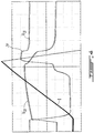
- FIG. 2 illustrates V ce , V ge and the current I at turn-off.
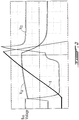
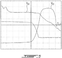
- Figure 3 shows the optimization of the overvoltage with a resistive divider technique and Figure 4 the associated wave shape for a bus voltage as high as 500 Vdc.
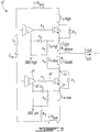
- the IGBT Q 1 includes a collector 14 having a parasitic inductance L c-low , an emitter 16 having a parasitic inductance L e-low and a gate 18 connected to the gate driver 20 via a resistor R 1 .
- the reference 22 of the gate driver 20 is connected to a resistive divider circuit including two resistors R 2 and R 3 and a diode D 3 that allows the turn-on not to be impacted.
- the values of the resistors R 2 and R 3 are selected according to the level of overvoltage allowed across Q 1 .
- Figure 4 show the result of a resistive divider optimized for an operation at a bus voltage of 500 Vdc and Figure 5 at a bus voltage of 300 Vdc.
- the ratio of R 2 over R 3 increases to reduce the overvoltage.
- the value of the two resistor in parallel is set, in series with R 1 , as the gate driver resistor. This value of the gate resistor is adjusted according to the proper commutation behavior.
- the normal practice consisting in using a resistor in the ground connection of the gate drive to limit the current in the diodes that protect the gate drive of the lower IGBT from a negative voltage when the upper IGBT turns off has been modified by splitting the resistor in two and adapt the ratio between them to limit the effect of the emitter inductance on the dl/dt.
- the total resistor remains the same but the voltage divider gives the desired weight of the emitter inductance to limit the overvoltage at the desired level.
- the overvoltage should obviously be optimized as much as possible to reach the maximum IGBT rating; this is done by reducing the resistor connected to the logical emitters R 3 compared to the resistor connected to the power tab R 2 .
- the voltage across the emitter inductance will be split in two and only the voltage across the logical resistor will be applied in the gate drive circuit to limit the gate voltage drop.
- resistors R 2 and R 3 are shown connected across both parasitic inductances L e-low and L -Vbus , they could be connected solely across parasitic inductance L e-low should this parasitic inductance be sufficient.
- Figure 4 shows the current I and the voltages V ge and V ce during turn-off for the circuit of Figure 3 .
- the overvoltage of V ce during turn-off is greatly reduced (see plateau 24). This plateau 24 occurs while the rate of drop of the voltage V ge is reduced by the insertion of the voltage from the parasitic inductance.
- the duration of the plateau will impact greatly the losses during turn-off: the longer the plateau, the higher the losses. Because of the desire to limit at the same time the overvoltage and its length, a square wave shape of the overvoltage plateau is suitable. The intrinsic behavior (natural feedback) of the overvoltage gives this shape.
- Figures 4 and 5 show the square shape of the overvoltage when using the resistive divider at different bus voltages.
- the upper and lower semiconductors are packaged within close proximity of each other so the inductance of the upper IGBT, L e-high , is quite small, in the order of a few nH.
- the inductance of the lower IGBT, L e-low is 5 times the upper emitter inductance L e-high .
- the connection of the -Vbus tab is highly inductive because of its length and curves.
- all IGBT modules have two power connections, part of the high-frequency loop, that are the most inductive: +Vbus and -Vbus. Because -Vbus is in the path of the emitter of the bottom IGBT, it can be used to inject a sample of the overvoltage across the IGBT in the gate driver of the bottom IGBT. Unfortunately, since the +Vbus connection is connected to the collector of the top IGBT, this inductance cannot be used directly as a feedback in the gate driver.
- Le-high As a feedback in the gate driver, it is therefore required to somehow increase its inductance without unduly increase the overall inductance of the high frequency loop. Two possible techniques to increase the L e-high inductance will be described hereinbelow.
- Figure 6 shows the connections of the transformer. More specifically, the primary of the transformer T1a is connected across the L c-high parasitic inductance while the secondary of the transformer T1b is connected in series with the resistor R 5 .
- Figure 7 of the appended drawings is a circuit diagram of an IGBT drive reducing the overvoltage by using a combination of a transformer and a resistive divider according to another illustrative embodiment.
- Figure 7 illustrates a circuit similar to that of Figure 6 .
- the main difference between these circuits is concerned with a resistive divider including resistors R 5 and R 6 enabling the fine tune of the shape of the negative slope of the V ge .
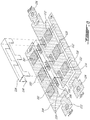
- the IGBTs 102 forming the IGBT Q2 have a collector mounted to a trace 104, the trace 104 therefore being referred to as C-High and their emitters are connected to emitter pads 106 via wire bonds 110.
- the IGBT 112 forming the IGBT Q1 have a collector mounted to a trace 114 therefore being referred to as C-Low and their emitters are connected to a trace 118 via wire bonds 120, the trace 118 therefore being referred to as E-Low.
- the trace 114 also has collector pads 116 that are connected thereto.
- the +Vbus tab is connected to trace 104 while the -Vbus tab is connected to trace 118.
- the phase tab 126 is connected to trace 114.
- the pads 106 and 116 are interconnected by a U-shaped connector128 having six (6) legs 130 so configured, sized and positioned as to connect to the pads 106 and 116.
- the U-shaped connector 128 defined the parasitic inductance L e-high since it interconnects the emitter of Q2 and the collector of Q1. Since the U-shape connector 128 is relatively large and includes right angles, the L e-high inductance is relatively high and can be used to limit the overvoltage in the IGBT Q2 as discussed hereinabove. It will also be understood that the size and shape of the connector 128 may be determined according to the desired parasitic inductance required.
- the main difference between the layout of Figure 8 and the layout of Figure 9 is the position of the tabs 106 which are positioned farther away from the pads 110 to thereby allow a larger connector 132 and therefore a larger parasitic inductance L e-high to be used.
Landscapes
- Engineering & Computer Science (AREA)
- Power Engineering (AREA)
- Power Conversion In General (AREA)
- Electronic Switches (AREA)
- Inverter Devices (AREA)
Applications Claiming Priority (2)
| Application Number | Priority Date | Filing Date | Title |
|---|---|---|---|
| US201161567800P | 2011-12-07 | 2011-12-07 | |
| PCT/CA2012/001125 WO2013082705A1 (en) | 2011-12-07 | 2012-12-05 | Turn-off overvoltage limiting for igbt |
Publications (3)
| Publication Number | Publication Date |
|---|---|
| EP2789092A1 EP2789092A1 (en) | 2014-10-15 |
| EP2789092A4 EP2789092A4 (en) | 2016-05-04 |
| EP2789092B1 true EP2789092B1 (en) | 2020-02-05 |
Family
ID=48573450
Family Applications (1)
| Application Number | Title | Priority Date | Filing Date |
|---|---|---|---|
| EP12856190.9A Active EP2789092B1 (en) | 2011-12-07 | 2012-12-05 | Turn-off overvoltage limiting for igbt |
Country Status (8)
| Country | Link |
|---|---|
| US (2) | US9608543B2 (enExample) |
| EP (1) | EP2789092B1 (enExample) |
| JP (1) | JP6239525B2 (enExample) |
| CN (1) | CN103988410B (enExample) |
| BR (1) | BR112014012206A2 (enExample) |
| CA (1) | CA2851376C (enExample) |
| IN (1) | IN2014DN03024A (enExample) |
| WO (1) | WO2013082705A1 (enExample) |
Families Citing this family (16)
| Publication number | Priority date | Publication date | Assignee | Title |
|---|---|---|---|---|
| CN103988410B (zh) * | 2011-12-07 | 2017-10-13 | Tm4股份有限公司 | 用于绝缘栅双极型晶体管的关断过电压限制 |
| US9112501B2 (en) * | 2012-09-29 | 2015-08-18 | Infineon Technologies Ag | Electronic circuit with an electronic switch and a monitoring circuit |
| CA2907472C (en) | 2013-04-04 | 2017-05-02 | Tm4 Inc. | Commutation cell and compensation circuit therefor |
| US9774244B2 (en) | 2013-11-01 | 2017-09-26 | Tm4 Inc. | Power converter configured for limiting switching overvoltage |
| CA2930187A1 (en) * | 2013-11-14 | 2015-05-21 | Tm4 Inc. | Commutation cell, power converter and compensation circuit having dynamically controlled voltage gains |
| WO2015070344A1 (en) | 2013-11-14 | 2015-05-21 | Tm4 Inc. | Compensation circuit, commutation cell and power converter controlling turn-on and turn-off of a power electronic switch |
| CA2989672C (en) | 2015-06-23 | 2022-11-29 | Tm4 Inc. | Physical topology for a power converter |
| US9812941B2 (en) | 2015-09-11 | 2017-11-07 | Nxp Usa, Inc. | High power driver having multiple turn off modes |
| WO2017045071A1 (en) * | 2015-09-14 | 2017-03-23 | Tm4 Inc. | Power converter configured for limiting switching overvoltage |
| CN107154791A (zh) * | 2016-03-02 | 2017-09-12 | 国网辽宁省电力有限公司电力科学研究院 | 高压大功率igbt模块的电流上升斜率检测电路及其检测方法 |
| US10122294B2 (en) | 2016-12-01 | 2018-11-06 | Ford Global Technologies, Llc | Active gate clamping for inverter switching devices with enhanced common source inductance |
| US9866099B1 (en) * | 2016-12-30 | 2018-01-09 | Texas Instruments Incorporated | Adaptive high-side gate drive for ringing mitigation in switching power converters |
| JP7341885B2 (ja) * | 2019-12-27 | 2023-09-11 | 川崎重工業株式会社 | スイッチング回路 |
| DE112021007336T5 (de) * | 2021-03-19 | 2023-12-28 | Mitsubishi Electric Corporation | Gleichstromversorgung, Kältekreislaufvorrichtung, Klimatisierungsvorrichtung und Kühlvorrichtung |
| WO2023001995A1 (fr) * | 2021-07-21 | 2023-01-26 | Valeo Systemes De Controle Moteur | Systeme de commutation et convertisseur de tension ou engin de mobilite comprenant un tel systeme de commutation |
| US12531554B2 (en) | 2023-02-27 | 2026-01-20 | Rtx Corporation | Enhanced solid state circuit breaker structure |
Family Cites Families (23)
| Publication number | Priority date | Publication date | Assignee | Title |
|---|---|---|---|---|
| JP3379556B2 (ja) * | 1993-12-30 | 2003-02-24 | サンケン電気株式会社 | スイッチング素子を有する回路装置 |
| KR100337035B1 (ko) * | 1999-11-26 | 2002-05-16 | 권영한 | 전력용 반도체 스위칭 소자의 직렬구동을 위한 수동형보조회로 |
| JP3598933B2 (ja) | 2000-02-28 | 2004-12-08 | 株式会社日立製作所 | 電力変換装置 |
| JP3932841B2 (ja) * | 2001-08-29 | 2007-06-20 | 株式会社日立製作所 | 半導体電力変換装置 |
| JP3731562B2 (ja) * | 2002-05-22 | 2006-01-05 | 日産自動車株式会社 | 電流制御型素子用駆動回路 |
| DE10231198A1 (de) * | 2002-07-10 | 2004-01-29 | eupec Europäische Gesellschaft für Leistungshalbleiter mbH | Verfahren und Schaltungsanordnung zum Begrenzen einer Überspannung |
| JP3975162B2 (ja) * | 2002-12-20 | 2007-09-12 | トヨタ自動車株式会社 | インバータ装置およびそれを用いた電動機一体インバータ装置 |
| JP4739059B2 (ja) | 2006-02-23 | 2011-08-03 | ルネサスエレクトロニクス株式会社 | Dc/dcコンバータ用半導体装置 |
| JP4432953B2 (ja) * | 2006-09-27 | 2010-03-17 | 株式会社日立製作所 | 半導体電力変換装置 |
| EP2434627A4 (en) * | 2009-05-19 | 2014-07-02 | Mitsubishi Electric Corp | GATE DRIVE CIRCUIT |
| US8149600B2 (en) | 2009-05-22 | 2012-04-03 | Infineon Technologies Ag | System and method for ringing suppression in a switched mode power supply |
| JP5315155B2 (ja) * | 2009-07-23 | 2013-10-16 | 日立オートモティブシステムズ株式会社 | 半導体素子制御装置、車載用電機システム |
| EP2526616A2 (en) | 2010-01-22 | 2012-11-28 | Massachusetts Institute of Technology | Grid-tied power conversion circuits and related techniques |
| KR101449083B1 (ko) * | 2010-05-06 | 2014-10-13 | 엘에스산전 주식회사 | 스위칭 게이트 드라이브 |
| US9793889B2 (en) * | 2011-03-15 | 2017-10-17 | Infineon Technologies Ag | Semiconductor device including a circuit to compensate for parasitic inductance |
| CN103988410B (zh) * | 2011-12-07 | 2017-10-13 | Tm4股份有限公司 | 用于绝缘栅双极型晶体管的关断过电压限制 |
| WO2013138219A1 (en) * | 2012-03-12 | 2013-09-19 | Board Of Trustees Of Michigan State University | High efficiency gate drive circuit for power transistors |
| WO2014043795A1 (en) * | 2012-09-24 | 2014-03-27 | Tm4 Inc. | Topology for controlled power switch module |
| CA2907472C (en) * | 2013-04-04 | 2017-05-02 | Tm4 Inc. | Commutation cell and compensation circuit therefor |
| US9774244B2 (en) * | 2013-11-01 | 2017-09-26 | Tm4 Inc. | Power converter configured for limiting switching overvoltage |
| CA2930187A1 (en) * | 2013-11-14 | 2015-05-21 | Tm4 Inc. | Commutation cell, power converter and compensation circuit having dynamically controlled voltage gains |
| WO2015070344A1 (en) * | 2013-11-14 | 2015-05-21 | Tm4 Inc. | Compensation circuit, commutation cell and power converter controlling turn-on and turn-off of a power electronic switch |
| US9608620B2 (en) * | 2013-12-03 | 2017-03-28 | Ingeteam Power Technology, S.A. | Control system and control method for controlling a switching device integrated in an electronic converter and switching cell comprising said system |
-
2012
- 2012-12-05 CN CN201280060186.9A patent/CN103988410B/zh active Active
- 2012-12-05 US US14/363,439 patent/US9608543B2/en active Active
- 2012-12-05 EP EP12856190.9A patent/EP2789092B1/en active Active
- 2012-12-05 CA CA2851376A patent/CA2851376C/en active Active
- 2012-12-05 BR BR112014012206A patent/BR112014012206A2/pt not_active IP Right Cessation
- 2012-12-05 WO PCT/CA2012/001125 patent/WO2013082705A1/en not_active Ceased
- 2012-12-05 JP JP2014545054A patent/JP6239525B2/ja not_active Expired - Fee Related
- 2012-12-05 IN IN3024DEN2014 patent/IN2014DN03024A/en unknown
-
2017
- 2017-02-13 US US15/431,418 patent/US10205405B2/en active Active
Non-Patent Citations (1)
| Title |
|---|
| None * |
Also Published As
| Publication number | Publication date |
|---|---|
| US9608543B2 (en) | 2017-03-28 |
| WO2013082705A1 (en) | 2013-06-13 |
| CN103988410B (zh) | 2017-10-13 |
| BR112014012206A2 (pt) | 2017-05-30 |
| CA2851376C (en) | 2021-02-16 |
| JP2015503319A (ja) | 2015-01-29 |
| IN2014DN03024A (enExample) | 2015-05-08 |
| US20170163172A1 (en) | 2017-06-08 |
| CA2851376A1 (en) | 2013-06-13 |
| CN103988410A (zh) | 2014-08-13 |
| US20140321178A1 (en) | 2014-10-30 |
| EP2789092A4 (en) | 2016-05-04 |
| JP6239525B2 (ja) | 2017-11-29 |
| EP2789092A1 (en) | 2014-10-15 |
| US10205405B2 (en) | 2019-02-12 |
Similar Documents
| Publication | Publication Date | Title |
|---|---|---|
| EP2789092B1 (en) | Turn-off overvoltage limiting for igbt | |
| US11979141B2 (en) | Efficient IGBT switching | |
| US10587257B2 (en) | Commutation cell and compensation circuit therefor | |
| US9812987B2 (en) | Topology for controlled power switch module | |
| US10277112B2 (en) | Physical topology for a power converter | |
| US9774244B2 (en) | Power converter configured for limiting switching overvoltage | |
| US10756648B2 (en) | Inverter system with enhanced common source inductance generated at gate driver | |
| CN108736703B (zh) | 最小化宽带隙半导体器件中的振铃 | |
| Zhou et al. | A low cost gate driver with dynamic turn-off transient control for HEV/EV traction inverter application | |
| HK1226873A1 (en) | Power converter configured for limiting switching overvoltage |
Legal Events
| Date | Code | Title | Description |
|---|---|---|---|
| PUAI | Public reference made under article 153(3) epc to a published international application that has entered the european phase |
Free format text: ORIGINAL CODE: 0009012 |
|
| 17P | Request for examination filed |
Effective date: 20140514 |
|
| AK | Designated contracting states |
Kind code of ref document: A1 Designated state(s): AL AT BE BG CH CY CZ DE DK EE ES FI FR GB GR HR HU IE IS IT LI LT LU LV MC MK MT NL NO PL PT RO RS SE SI SK SM TR |
|
| RIN1 | Information on inventor provided before grant (corrected) |
Inventor name: AMAR, MOHAMMED Inventor name: FLEURY, PASCAL Inventor name: CYR, JEAN-MARC Inventor name: EL YACOUBI, MAALAININE |
|
| DAX | Request for extension of the european patent (deleted) | ||
| RA4 | Supplementary search report drawn up and despatched (corrected) |
Effective date: 20160404 |
|
| RIC1 | Information provided on ipc code assigned before grant |
Ipc: H02M 1/08 20060101ALI20160329BHEP Ipc: H03K 17/082 20060101ALI20160329BHEP Ipc: H02M 1/32 20070101ALI20160329BHEP Ipc: H03K 17/16 20060101ALI20160329BHEP Ipc: H03K 17/60 20060101ALI20160329BHEP Ipc: H02M 7/537 20060101ALI20160329BHEP Ipc: H02M 7/217 20060101AFI20160329BHEP Ipc: H02M 1/00 20060101ALI20160329BHEP |
|
| STAA | Information on the status of an ep patent application or granted ep patent |
Free format text: STATUS: EXAMINATION IS IN PROGRESS |
|
| 17Q | First examination report despatched |
Effective date: 20181016 |
|
| GRAP | Despatch of communication of intention to grant a patent |
Free format text: ORIGINAL CODE: EPIDOSNIGR1 |
|
| STAA | Information on the status of an ep patent application or granted ep patent |
Free format text: STATUS: GRANT OF PATENT IS INTENDED |
|
| INTG | Intention to grant announced |
Effective date: 20190715 |
|
| GRAS | Grant fee paid |
Free format text: ORIGINAL CODE: EPIDOSNIGR3 |
|
| GRAA | (expected) grant |
Free format text: ORIGINAL CODE: 0009210 |
|
| STAA | Information on the status of an ep patent application or granted ep patent |
Free format text: STATUS: THE PATENT HAS BEEN GRANTED |
|
| AK | Designated contracting states |
Kind code of ref document: B1 Designated state(s): AL AT BE BG CH CY CZ DE DK EE ES FI FR GB GR HR HU IE IS IT LI LT LU LV MC MK MT NL NO PL PT RO RS SE SI SK SM TR |
|
| REG | Reference to a national code |
Ref country code: GB Ref legal event code: FG4D |
|
| REG | Reference to a national code |
Ref country code: AT Ref legal event code: REF Ref document number: 1230571 Country of ref document: AT Kind code of ref document: T Effective date: 20200215 |
|
| REG | Reference to a national code |
Ref country code: DE Ref legal event code: R096 Ref document number: 602012067603 Country of ref document: DE |
|
| REG | Reference to a national code |
Ref country code: IE Ref legal event code: FG4D |
|
| REG | Reference to a national code |
Ref country code: CH Ref legal event code: EP |
|
| REG | Reference to a national code |
Ref country code: NL Ref legal event code: MP Effective date: 20200205 |
|
| PG25 | Lapsed in a contracting state [announced via postgrant information from national office to epo] |
Ref country code: NO Free format text: LAPSE BECAUSE OF FAILURE TO SUBMIT A TRANSLATION OF THE DESCRIPTION OR TO PAY THE FEE WITHIN THE PRESCRIBED TIME-LIMIT Effective date: 20200505 Ref country code: PT Free format text: LAPSE BECAUSE OF FAILURE TO SUBMIT A TRANSLATION OF THE DESCRIPTION OR TO PAY THE FEE WITHIN THE PRESCRIBED TIME-LIMIT Effective date: 20200628 Ref country code: FI Free format text: LAPSE BECAUSE OF FAILURE TO SUBMIT A TRANSLATION OF THE DESCRIPTION OR TO PAY THE FEE WITHIN THE PRESCRIBED TIME-LIMIT Effective date: 20200205 Ref country code: RS Free format text: LAPSE BECAUSE OF FAILURE TO SUBMIT A TRANSLATION OF THE DESCRIPTION OR TO PAY THE FEE WITHIN THE PRESCRIBED TIME-LIMIT Effective date: 20200205 |
|
| REG | Reference to a national code |
Ref country code: LT Ref legal event code: MG4D |
|
| RAP2 | Party data changed (patent owner data changed or rights of a patent transferred) |
Owner name: DANA TM4 INC. |
|
| PG25 | Lapsed in a contracting state [announced via postgrant information from national office to epo] |
Ref country code: BG Free format text: LAPSE BECAUSE OF FAILURE TO SUBMIT A TRANSLATION OF THE DESCRIPTION OR TO PAY THE FEE WITHIN THE PRESCRIBED TIME-LIMIT Effective date: 20200505 Ref country code: IS Free format text: LAPSE BECAUSE OF FAILURE TO SUBMIT A TRANSLATION OF THE DESCRIPTION OR TO PAY THE FEE WITHIN THE PRESCRIBED TIME-LIMIT Effective date: 20200605 Ref country code: GR Free format text: LAPSE BECAUSE OF FAILURE TO SUBMIT A TRANSLATION OF THE DESCRIPTION OR TO PAY THE FEE WITHIN THE PRESCRIBED TIME-LIMIT Effective date: 20200506 Ref country code: SE Free format text: LAPSE BECAUSE OF FAILURE TO SUBMIT A TRANSLATION OF THE DESCRIPTION OR TO PAY THE FEE WITHIN THE PRESCRIBED TIME-LIMIT Effective date: 20200205 Ref country code: LV Free format text: LAPSE BECAUSE OF FAILURE TO SUBMIT A TRANSLATION OF THE DESCRIPTION OR TO PAY THE FEE WITHIN THE PRESCRIBED TIME-LIMIT Effective date: 20200205 Ref country code: HR Free format text: LAPSE BECAUSE OF FAILURE TO SUBMIT A TRANSLATION OF THE DESCRIPTION OR TO PAY THE FEE WITHIN THE PRESCRIBED TIME-LIMIT Effective date: 20200205 |
|
| PG25 | Lapsed in a contracting state [announced via postgrant information from national office to epo] |
Ref country code: NL Free format text: LAPSE BECAUSE OF FAILURE TO SUBMIT A TRANSLATION OF THE DESCRIPTION OR TO PAY THE FEE WITHIN THE PRESCRIBED TIME-LIMIT Effective date: 20200205 |
|
| REG | Reference to a national code |
Ref country code: DE Ref legal event code: R081 Ref document number: 602012067603 Country of ref document: DE Owner name: DANA TM4 INC., BOUCHERVILLE, CA Free format text: FORMER OWNER: TM4 INC., BOUCHERVILLE, QUEBEC, CA |
|
| PG25 | Lapsed in a contracting state [announced via postgrant information from national office to epo] |
Ref country code: DK Free format text: LAPSE BECAUSE OF FAILURE TO SUBMIT A TRANSLATION OF THE DESCRIPTION OR TO PAY THE FEE WITHIN THE PRESCRIBED TIME-LIMIT Effective date: 20200205 Ref country code: SM Free format text: LAPSE BECAUSE OF FAILURE TO SUBMIT A TRANSLATION OF THE DESCRIPTION OR TO PAY THE FEE WITHIN THE PRESCRIBED TIME-LIMIT Effective date: 20200205 Ref country code: EE Free format text: LAPSE BECAUSE OF FAILURE TO SUBMIT A TRANSLATION OF THE DESCRIPTION OR TO PAY THE FEE WITHIN THE PRESCRIBED TIME-LIMIT Effective date: 20200205 Ref country code: LT Free format text: LAPSE BECAUSE OF FAILURE TO SUBMIT A TRANSLATION OF THE DESCRIPTION OR TO PAY THE FEE WITHIN THE PRESCRIBED TIME-LIMIT Effective date: 20200205 Ref country code: ES Free format text: LAPSE BECAUSE OF FAILURE TO SUBMIT A TRANSLATION OF THE DESCRIPTION OR TO PAY THE FEE WITHIN THE PRESCRIBED TIME-LIMIT Effective date: 20200205 Ref country code: SK Free format text: LAPSE BECAUSE OF FAILURE TO SUBMIT A TRANSLATION OF THE DESCRIPTION OR TO PAY THE FEE WITHIN THE PRESCRIBED TIME-LIMIT Effective date: 20200205 Ref country code: RO Free format text: LAPSE BECAUSE OF FAILURE TO SUBMIT A TRANSLATION OF THE DESCRIPTION OR TO PAY THE FEE WITHIN THE PRESCRIBED TIME-LIMIT Effective date: 20200205 Ref country code: CZ Free format text: LAPSE BECAUSE OF FAILURE TO SUBMIT A TRANSLATION OF THE DESCRIPTION OR TO PAY THE FEE WITHIN THE PRESCRIBED TIME-LIMIT Effective date: 20200205 |
|
| REG | Reference to a national code |
Ref country code: DE Ref legal event code: R097 Ref document number: 602012067603 Country of ref document: DE |
|
| REG | Reference to a national code |
Ref country code: AT Ref legal event code: MK05 Ref document number: 1230571 Country of ref document: AT Kind code of ref document: T Effective date: 20200205 |
|
| PLBE | No opposition filed within time limit |
Free format text: ORIGINAL CODE: 0009261 |
|
| STAA | Information on the status of an ep patent application or granted ep patent |
Free format text: STATUS: NO OPPOSITION FILED WITHIN TIME LIMIT |
|
| 26N | No opposition filed |
Effective date: 20201106 |
|
| PG25 | Lapsed in a contracting state [announced via postgrant information from national office to epo] |
Ref country code: AT Free format text: LAPSE BECAUSE OF FAILURE TO SUBMIT A TRANSLATION OF THE DESCRIPTION OR TO PAY THE FEE WITHIN THE PRESCRIBED TIME-LIMIT Effective date: 20200205 Ref country code: IT Free format text: LAPSE BECAUSE OF FAILURE TO SUBMIT A TRANSLATION OF THE DESCRIPTION OR TO PAY THE FEE WITHIN THE PRESCRIBED TIME-LIMIT Effective date: 20200205 |
|
| PG25 | Lapsed in a contracting state [announced via postgrant information from national office to epo] |
Ref country code: PL Free format text: LAPSE BECAUSE OF FAILURE TO SUBMIT A TRANSLATION OF THE DESCRIPTION OR TO PAY THE FEE WITHIN THE PRESCRIBED TIME-LIMIT Effective date: 20200205 Ref country code: SI Free format text: LAPSE BECAUSE OF FAILURE TO SUBMIT A TRANSLATION OF THE DESCRIPTION OR TO PAY THE FEE WITHIN THE PRESCRIBED TIME-LIMIT Effective date: 20200205 |
|
| REG | Reference to a national code |
Ref country code: CH Ref legal event code: PL |
|
| GBPC | Gb: european patent ceased through non-payment of renewal fee |
Effective date: 20201205 |
|
| PG25 | Lapsed in a contracting state [announced via postgrant information from national office to epo] |
Ref country code: MC Free format text: LAPSE BECAUSE OF FAILURE TO SUBMIT A TRANSLATION OF THE DESCRIPTION OR TO PAY THE FEE WITHIN THE PRESCRIBED TIME-LIMIT Effective date: 20200205 |
|
| REG | Reference to a national code |
Ref country code: BE Ref legal event code: MM Effective date: 20201231 |
|
| PG25 | Lapsed in a contracting state [announced via postgrant information from national office to epo] |
Ref country code: IE Free format text: LAPSE BECAUSE OF NON-PAYMENT OF DUE FEES Effective date: 20201205 Ref country code: LU Free format text: LAPSE BECAUSE OF NON-PAYMENT OF DUE FEES Effective date: 20201205 Ref country code: FR Free format text: LAPSE BECAUSE OF NON-PAYMENT OF DUE FEES Effective date: 20201231 |
|
| PG25 | Lapsed in a contracting state [announced via postgrant information from national office to epo] |
Ref country code: GB Free format text: LAPSE BECAUSE OF NON-PAYMENT OF DUE FEES Effective date: 20201205 Ref country code: CH Free format text: LAPSE BECAUSE OF NON-PAYMENT OF DUE FEES Effective date: 20201231 Ref country code: LI Free format text: LAPSE BECAUSE OF NON-PAYMENT OF DUE FEES Effective date: 20201231 |
|
| PG25 | Lapsed in a contracting state [announced via postgrant information from national office to epo] |
Ref country code: TR Free format text: LAPSE BECAUSE OF FAILURE TO SUBMIT A TRANSLATION OF THE DESCRIPTION OR TO PAY THE FEE WITHIN THE PRESCRIBED TIME-LIMIT Effective date: 20200205 Ref country code: MT Free format text: LAPSE BECAUSE OF FAILURE TO SUBMIT A TRANSLATION OF THE DESCRIPTION OR TO PAY THE FEE WITHIN THE PRESCRIBED TIME-LIMIT Effective date: 20200205 Ref country code: CY Free format text: LAPSE BECAUSE OF FAILURE TO SUBMIT A TRANSLATION OF THE DESCRIPTION OR TO PAY THE FEE WITHIN THE PRESCRIBED TIME-LIMIT Effective date: 20200205 |
|
| PG25 | Lapsed in a contracting state [announced via postgrant information from national office to epo] |
Ref country code: MK Free format text: LAPSE BECAUSE OF FAILURE TO SUBMIT A TRANSLATION OF THE DESCRIPTION OR TO PAY THE FEE WITHIN THE PRESCRIBED TIME-LIMIT Effective date: 20200205 Ref country code: AL Free format text: LAPSE BECAUSE OF FAILURE TO SUBMIT A TRANSLATION OF THE DESCRIPTION OR TO PAY THE FEE WITHIN THE PRESCRIBED TIME-LIMIT Effective date: 20200205 |
|
| PG25 | Lapsed in a contracting state [announced via postgrant information from national office to epo] |
Ref country code: BE Free format text: LAPSE BECAUSE OF NON-PAYMENT OF DUE FEES Effective date: 20201231 |
|
| P01 | Opt-out of the competence of the unified patent court (upc) registered |
Effective date: 20230524 |
|
| PGFP | Annual fee paid to national office [announced via postgrant information from national office to epo] |
Ref country code: DE Payment date: 20251126 Year of fee payment: 14 |