EP2789060B1 - Edge-emitting etched-facet lasers - Google Patents
Edge-emitting etched-facet lasers Download PDFInfo
- Publication number
- EP2789060B1 EP2789060B1 EP12855851.7A EP12855851A EP2789060B1 EP 2789060 B1 EP2789060 B1 EP 2789060B1 EP 12855851 A EP12855851 A EP 12855851A EP 2789060 B1 EP2789060 B1 EP 2789060B1
- Authority
- EP
- European Patent Office
- Prior art keywords
- waveguide
- laser
- etched facet
- recessed region
- facet
- Prior art date
- Legal status (The legal status is an assumption and is not a legal conclusion. Google has not performed a legal analysis and makes no representation as to the accuracy of the status listed.)
- Active
Links
Images




Classifications
-
- H—ELECTRICITY
- H01—ELECTRIC ELEMENTS
- H01S—DEVICES USING THE PROCESS OF LIGHT AMPLIFICATION BY STIMULATED EMISSION OF RADIATION [LASER] TO AMPLIFY OR GENERATE LIGHT; DEVICES USING STIMULATED EMISSION OF ELECTROMAGNETIC RADIATION IN WAVE RANGES OTHER THAN OPTICAL
- H01S5/00—Semiconductor lasers
- H01S5/0014—Measuring characteristics or properties thereof
-
- H—ELECTRICITY
- H01—ELECTRIC ELEMENTS
- H01S—DEVICES USING THE PROCESS OF LIGHT AMPLIFICATION BY STIMULATED EMISSION OF RADIATION [LASER] TO AMPLIFY OR GENERATE LIGHT; DEVICES USING STIMULATED EMISSION OF ELECTROMAGNETIC RADIATION IN WAVE RANGES OTHER THAN OPTICAL
- H01S5/00—Semiconductor lasers
- H01S5/0014—Measuring characteristics or properties thereof
- H01S5/0042—On wafer testing, e.g. lasers are tested before separating wafer into chips
-
- G—PHYSICS
- G01—MEASURING; TESTING
- G01R—MEASURING ELECTRIC VARIABLES; MEASURING MAGNETIC VARIABLES
- G01R31/00—Arrangements for testing electric properties; Arrangements for locating electric faults; Arrangements for electrical testing characterised by what is being tested not provided for elsewhere
- G01R31/26—Testing of individual semiconductor devices
-
- H—ELECTRICITY
- H01—ELECTRIC ELEMENTS
- H01S—DEVICES USING THE PROCESS OF LIGHT AMPLIFICATION BY STIMULATED EMISSION OF RADIATION [LASER] TO AMPLIFY OR GENERATE LIGHT; DEVICES USING STIMULATED EMISSION OF ELECTROMAGNETIC RADIATION IN WAVE RANGES OTHER THAN OPTICAL
- H01S5/00—Semiconductor lasers
- H01S5/02—Structural details or components not essential to laser action
- H01S5/0201—Separation of the wafer into individual elements, e.g. by dicing, cleaving, etching or directly during growth
- H01S5/0203—Etching
-
- H—ELECTRICITY
- H01—ELECTRIC ELEMENTS
- H01S—DEVICES USING THE PROCESS OF LIGHT AMPLIFICATION BY STIMULATED EMISSION OF RADIATION [LASER] TO AMPLIFY OR GENERATE LIGHT; DEVICES USING STIMULATED EMISSION OF ELECTROMAGNETIC RADIATION IN WAVE RANGES OTHER THAN OPTICAL
- H01S5/00—Semiconductor lasers
- H01S5/02—Structural details or components not essential to laser action
- H01S5/028—Coatings ; Treatment of the laser facets, e.g. etching, passivation layers or reflecting layers
- H01S5/0287—Facet reflectivity
-
- H—ELECTRICITY
- H01—ELECTRIC ELEMENTS
- H01S—DEVICES USING THE PROCESS OF LIGHT AMPLIFICATION BY STIMULATED EMISSION OF RADIATION [LASER] TO AMPLIFY OR GENERATE LIGHT; DEVICES USING STIMULATED EMISSION OF ELECTROMAGNETIC RADIATION IN WAVE RANGES OTHER THAN OPTICAL
- H01S5/00—Semiconductor lasers
- H01S5/10—Construction or shape of the optical resonator, e.g. extended or external cavity, coupled cavities, bent-guide, varying width, thickness or composition of the active region
- H01S5/1003—Waveguide having a modified shape along the axis, e.g. branched, curved, tapered, voids
- H01S5/1014—Tapered waveguide, e.g. spotsize converter
-
- H—ELECTRICITY
- H01—ELECTRIC ELEMENTS
- H01S—DEVICES USING THE PROCESS OF LIGHT AMPLIFICATION BY STIMULATED EMISSION OF RADIATION [LASER] TO AMPLIFY OR GENERATE LIGHT; DEVICES USING STIMULATED EMISSION OF ELECTROMAGNETIC RADIATION IN WAVE RANGES OTHER THAN OPTICAL
- H01S5/00—Semiconductor lasers
- H01S5/10—Construction or shape of the optical resonator, e.g. extended or external cavity, coupled cavities, bent-guide, varying width, thickness or composition of the active region
- H01S5/12—Construction or shape of the optical resonator, e.g. extended or external cavity, coupled cavities, bent-guide, varying width, thickness or composition of the active region the resonator having a periodic structure, e.g. in distributed feedback [DFB] lasers
-
- H—ELECTRICITY
- H01—ELECTRIC ELEMENTS
- H01S—DEVICES USING THE PROCESS OF LIGHT AMPLIFICATION BY STIMULATED EMISSION OF RADIATION [LASER] TO AMPLIFY OR GENERATE LIGHT; DEVICES USING STIMULATED EMISSION OF ELECTROMAGNETIC RADIATION IN WAVE RANGES OTHER THAN OPTICAL
- H01S5/00—Semiconductor lasers
- H01S5/20—Structure or shape of the semiconductor body to guide the optical wave ; Confining structures perpendicular to the optical axis, e.g. index or gain guiding, stripe geometry, broad area lasers, gain tailoring, transverse or lateral reflectors, special cladding structures, MQW barrier reflection layers
-
- H—ELECTRICITY
- H01—ELECTRIC ELEMENTS
- H01S—DEVICES USING THE PROCESS OF LIGHT AMPLIFICATION BY STIMULATED EMISSION OF RADIATION [LASER] TO AMPLIFY OR GENERATE LIGHT; DEVICES USING STIMULATED EMISSION OF ELECTROMAGNETIC RADIATION IN WAVE RANGES OTHER THAN OPTICAL
- H01S5/00—Semiconductor lasers
- H01S5/20—Structure or shape of the semiconductor body to guide the optical wave ; Confining structures perpendicular to the optical axis, e.g. index or gain guiding, stripe geometry, broad area lasers, gain tailoring, transverse or lateral reflectors, special cladding structures, MQW barrier reflection layers
- H01S5/22—Structure or shape of the semiconductor body to guide the optical wave ; Confining structures perpendicular to the optical axis, e.g. index or gain guiding, stripe geometry, broad area lasers, gain tailoring, transverse or lateral reflectors, special cladding structures, MQW barrier reflection layers having a ridge or stripe structure
-
- H—ELECTRICITY
- H01—ELECTRIC ELEMENTS
- H01S—DEVICES USING THE PROCESS OF LIGHT AMPLIFICATION BY STIMULATED EMISSION OF RADIATION [LASER] TO AMPLIFY OR GENERATE LIGHT; DEVICES USING STIMULATED EMISSION OF ELECTROMAGNETIC RADIATION IN WAVE RANGES OTHER THAN OPTICAL
- H01S5/00—Semiconductor lasers
- H01S5/20—Structure or shape of the semiconductor body to guide the optical wave ; Confining structures perpendicular to the optical axis, e.g. index or gain guiding, stripe geometry, broad area lasers, gain tailoring, transverse or lateral reflectors, special cladding structures, MQW barrier reflection layers
- H01S5/22—Structure or shape of the semiconductor body to guide the optical wave ; Confining structures perpendicular to the optical axis, e.g. index or gain guiding, stripe geometry, broad area lasers, gain tailoring, transverse or lateral reflectors, special cladding structures, MQW barrier reflection layers having a ridge or stripe structure
- H01S5/223—Buried stripe structure
-
- H—ELECTRICITY
- H01—ELECTRIC ELEMENTS
- H01S—DEVICES USING THE PROCESS OF LIGHT AMPLIFICATION BY STIMULATED EMISSION OF RADIATION [LASER] TO AMPLIFY OR GENERATE LIGHT; DEVICES USING STIMULATED EMISSION OF ELECTROMAGNETIC RADIATION IN WAVE RANGES OTHER THAN OPTICAL
- H01S5/00—Semiconductor lasers
- H01S5/30—Structure or shape of the active region; Materials used for the active region
- H01S5/34—Structure or shape of the active region; Materials used for the active region comprising quantum well or superlattice structures, e.g. single quantum well [SQW] lasers, multiple quantum well [MQW] lasers or graded index separate confinement heterostructure [GRINSCH] lasers
- H01S5/343—Structure or shape of the active region; Materials used for the active region comprising quantum well or superlattice structures, e.g. single quantum well [SQW] lasers, multiple quantum well [MQW] lasers or graded index separate confinement heterostructure [GRINSCH] lasers in AIIIBV compounds, e.g. AlGaAs-laser, InP-based laser
- H01S5/34306—Structure or shape of the active region; Materials used for the active region comprising quantum well or superlattice structures, e.g. single quantum well [SQW] lasers, multiple quantum well [MQW] lasers or graded index separate confinement heterostructure [GRINSCH] lasers in AIIIBV compounds, e.g. AlGaAs-laser, InP-based laser emitting light at a wavelength longer than 1000nm, e.g. InP based 1300 and 1500nm lasers
-
- H—ELECTRICITY
- H01—ELECTRIC ELEMENTS
- H01S—DEVICES USING THE PROCESS OF LIGHT AMPLIFICATION BY STIMULATED EMISSION OF RADIATION [LASER] TO AMPLIFY OR GENERATE LIGHT; DEVICES USING STIMULATED EMISSION OF ELECTROMAGNETIC RADIATION IN WAVE RANGES OTHER THAN OPTICAL
- H01S5/00—Semiconductor lasers
- H01S5/30—Structure or shape of the active region; Materials used for the active region
- H01S5/34—Structure or shape of the active region; Materials used for the active region comprising quantum well or superlattice structures, e.g. single quantum well [SQW] lasers, multiple quantum well [MQW] lasers or graded index separate confinement heterostructure [GRINSCH] lasers
- H01S5/343—Structure or shape of the active region; Materials used for the active region comprising quantum well or superlattice structures, e.g. single quantum well [SQW] lasers, multiple quantum well [MQW] lasers or graded index separate confinement heterostructure [GRINSCH] lasers in AIIIBV compounds, e.g. AlGaAs-laser, InP-based laser
- H01S5/34313—Structure or shape of the active region; Materials used for the active region comprising quantum well or superlattice structures, e.g. single quantum well [SQW] lasers, multiple quantum well [MQW] lasers or graded index separate confinement heterostructure [GRINSCH] lasers in AIIIBV compounds, e.g. AlGaAs-laser, InP-based laser with a well layer having only As as V-compound, e.g. AlGaAs, InGaAs
-
- H—ELECTRICITY
- H01—ELECTRIC ELEMENTS
- H01S—DEVICES USING THE PROCESS OF LIGHT AMPLIFICATION BY STIMULATED EMISSION OF RADIATION [LASER] TO AMPLIFY OR GENERATE LIGHT; DEVICES USING STIMULATED EMISSION OF ELECTROMAGNETIC RADIATION IN WAVE RANGES OTHER THAN OPTICAL
- H01S5/00—Semiconductor lasers
- H01S5/30—Structure or shape of the active region; Materials used for the active region
- H01S5/34—Structure or shape of the active region; Materials used for the active region comprising quantum well or superlattice structures, e.g. single quantum well [SQW] lasers, multiple quantum well [MQW] lasers or graded index separate confinement heterostructure [GRINSCH] lasers
- H01S5/343—Structure or shape of the active region; Materials used for the active region comprising quantum well or superlattice structures, e.g. single quantum well [SQW] lasers, multiple quantum well [MQW] lasers or graded index separate confinement heterostructure [GRINSCH] lasers in AIIIBV compounds, e.g. AlGaAs-laser, InP-based laser
- H01S5/34333—Structure or shape of the active region; Materials used for the active region comprising quantum well or superlattice structures, e.g. single quantum well [SQW] lasers, multiple quantum well [MQW] lasers or graded index separate confinement heterostructure [GRINSCH] lasers in AIIIBV compounds, e.g. AlGaAs-laser, InP-based laser with a well layer based on Ga(In)N or Ga(In)P, e.g. blue laser
-
- G—PHYSICS
- G01—MEASURING; TESTING
- G01R—MEASURING ELECTRIC VARIABLES; MEASURING MAGNETIC VARIABLES
- G01R31/00—Arrangements for testing electric properties; Arrangements for locating electric faults; Arrangements for electrical testing characterised by what is being tested not provided for elsewhere
- G01R31/26—Testing of individual semiconductor devices
- G01R31/2607—Circuits therefor
- G01R31/2632—Circuits therefor for testing diodes
- G01R31/2635—Testing light-emitting diodes, laser diodes or photodiodes
-
- H—ELECTRICITY
- H01—ELECTRIC ELEMENTS
- H01S—DEVICES USING THE PROCESS OF LIGHT AMPLIFICATION BY STIMULATED EMISSION OF RADIATION [LASER] TO AMPLIFY OR GENERATE LIGHT; DEVICES USING STIMULATED EMISSION OF ELECTROMAGNETIC RADIATION IN WAVE RANGES OTHER THAN OPTICAL
- H01S5/00—Semiconductor lasers
- H01S5/02—Structural details or components not essential to laser action
- H01S5/0201—Separation of the wafer into individual elements, e.g. by dicing, cleaving, etching or directly during growth
-
- H—ELECTRICITY
- H01—ELECTRIC ELEMENTS
- H01S—DEVICES USING THE PROCESS OF LIGHT AMPLIFICATION BY STIMULATED EMISSION OF RADIATION [LASER] TO AMPLIFY OR GENERATE LIGHT; DEVICES USING STIMULATED EMISSION OF ELECTROMAGNETIC RADIATION IN WAVE RANGES OTHER THAN OPTICAL
- H01S5/00—Semiconductor lasers
- H01S5/02—Structural details or components not essential to laser action
- H01S5/028—Coatings ; Treatment of the laser facets, e.g. etching, passivation layers or reflecting layers
Definitions
- the present invention relates, in general, to etched-facet photonic devices, and more particularly to improved etched-facet photonic devices and methods for fabricating them.
- Semiconductor lasers typically are fabricated on a wafer by growing an appropriate layered semiconductor material on a substrate through Metalorganic Chemical Vapor Deposition (MOCVD) or Molecular Beam Epitaxy (MBE) to form an epitaxial structure having an active layer parallel to the substrate surface.
- MOCVD Metalorganic Chemical Vapor Deposition
- MBE Molecular Beam Epitaxy
- the wafer is then processed with a variety of semiconductor processing tools to produce a laser optical cavity incorporating the active layer and incorporating metallic contacts attached to the semiconductor material.
- Laser mirror facets typically are formed at the ends of the laser cavity by cleaving the semiconductor material along its crystalline structure to define edges, or ends, of the laser optical cavity so that when a bias voltage is applied across the contacts, the resulting current flow through the active layer causes photons to be emitted out of the faceted edges of the active layer in a direction perpendicular to the current flow. Since the semiconductor material is cleaved to form the laser facets, the locations and orientations of the facets are limited; furthermore, once the wafer has been cleaved it typically is in small pieces so that conventional lithographical techniques cannot readily be used to further process the lasers.
- FP and DFB edge-emitting lasers fabricated using etched facets could not be closely packed because of the interference of the laser output from a front facet of laser to the back facet of the adjacent laser that would distort on-wafer test results.
- the solution has been to space out lasers, leaving wasted space between adjacent lasers. For example, for a DFB laser, this wasted space is on the order of 100 ⁇ m that significantly reduces the number of useful laser chips that can be produced from a given wafer.
- US 5032879 discloses an integrated semiconductor structure with optically coupled laser diode and photodiode, both devices having etched, vertical facets.
- the photodiode has a spatially non-uniform sensitivity profile with respect to the incident light beam emitted by the laser, which allows the measurement of the far-field intensity distribution of the laser and thus on-wafer screening of lasers with respect to their mode-stability.
- US 2008/017868 discloses a semiconductor laser device including: semiconductor layers including an n-type semiconductor layer, an active layer and a p-type semiconductor layer, the semiconductor layers having a stripe-shaped waveguide region formed therein; end face protective film formed on the end face of the semiconductor layer that is substantially perpendicular to the waveguide region; wherein a p-side protruding portion is formed in the vicinity of the end portion of a p-electrode or n-electrode.
- US 2007/045637 discloses a method and structure for producing lasers, which includes providing a laser wherein an output beam emerging from the laser front facet is essentially unobstructed by the edges of the semiconductor chip in order to prevent detrimental beam distortions.
- the semiconductor laser structure is epitaxially grown on a substrate with at least a lower cladding layer, an active layer, an upper cladding layer, and a contact layer. Dry etching through a lithographically defined mask produces a laser mesa of length Ic and width bm. Another sequence of lithography and etching is used to form a ridge structure with width w on top of the mesa.
- the etching step also forming mirrors, or facets, on the ends of the laser waveguide structures.
- the length Is and width bs of the chip can be selected as convenient values equal to or longer than the waveguide length Ic and mesa width bm, respectively.
- the waveguide length and width are selected so that for a given defect density D, the yield YD is larger than 50%.
- the invention relates to a laser structure as defined in claim 1, a method of fabricating a semiconductor laser structure as defined in claim 12 and a method of testing semiconductor lasers as defined in claim 13. Further embodiments are subject of the dependent claims.
- the idea underlying the present invention is to provide edge-emitting lasers that are able to be fabricated with minimal wasted space between adjacent lasers.
- the front etched facet of a laser is facing a recessed region on the back side of the adjacent laser chip so that the light from the front facet of a first laser can exit without interference and back-reflection from the back facet of a second adjacent laser.
- the invention yields a chip with a first etched-facet edge-emitting semiconductor laser that contains a recessed region to allow a second etched-facet edge-emitting semiconductor laser, adjacent to the chip containing the first laser and with its front-facet facing the chip, to be closely spaced to each other while avoiding distortion during the testing of the characteristics of the second laser. This allows a significant increase in the number of chips that can be produced from a wafer.
- the recessed region can have a slanted end wall to minimize back-reflection.
- the back facet of a laser may also face a recessed region on the front side of the adjacent laser chip and the recessed region may have an angled end wall.
- Chips may have a complete recessed region or complete opening along their length and offset from each other to minimize back reflection.
- Fig. 1 shows a perspective view of a substrate 90 with an epitaxially deposited waveguide structure including an active region 80 in which etched-facet lasers including a ridge 40 are fabricated.
- the etched-facet ridge laser mesas 10 and 20 are positioned on the substrate so that the front facet 50 of laser corresponding to mesa 10 is at a distance 70 from the back facet of laser corresponding to mesa 20.
- Fig. 2 shows a top plan view of two adjacent etched-facet ridge lasers, similar to those in Fig. 1 .
- a wire-bond pad 30 is provided to allow wire-bonding to the pad and for electric current to be directed to the ridge allowing the laser to operate.
- the laser mesas 10 and 20 are positioned on chip 15 and 25, respectively.
- the chips 15 and 25 are formed through a singulation process along the lines that define the boundary of the chips in Fig. 2 .
- the substrate 90 may be formed, for example, of a type III-V compound, or an alloy thereof, which may be suitably doped.
- the substrate such as InP, includes a top surface on which is deposited, as by an epitaxial deposition such as Metalorganic Chemical Vapor Deposition (MOCVD) or Molecular Beam Epitaxy (MBE), a succession of layers which form an optical waveguide that includes an active region 80.
- MOCVD Metalorganic Chemical Vapor Deposition
- MBE Molecular Beam Epitaxy
- the semiconductor laser structure may contain upper and lower cladding regions, formed from lower index semiconductor material than the active region 80, such as InP, adjacent the active region 80, which may be formed with InAIGaAs-based quantum wells and barriers.
- the lower cladding may be formed partially through the epitaxial deposition and partly by using the substrate.
- a 1310nm emitting epitaxial structure can be used with the following layers on an InP substrate 90: 0.5 ⁇ m n-InP; 0.105 ⁇ m AlGaInAs lower graded region; an active region 80 containing five 6nm thick compressively strained AlGaInAs quantum wells, each sandwiched by 10nm tensile strained AlGaInAs barriers; 0.105 ⁇ m AlGaInAs upper graded region; 1.65 ⁇ m thick p-InP upper cladding; and highly p-doped InGaAs cap layer.
- the structure may also have a wet etch stop layer.
- etched-facet lasers One of the key benefits of etched-facet lasers is that testing is performed at wafer-level as opposed to bar-level testing for cleaved-facet lasers.
- the distance 70 has to be large enough to prevent the adverse impact of back-reflection and interference from back-facet 60 to front facet 50.
- the front facet 50 is where most of the light emerges from the edge-emitting laser corresponding to mesa 10.
- the distance 70 is 50 ⁇ m for an InP-based 1310nm Fabry-Perot (FP) ridge laser of ridge width of about 2 ⁇ m, the undesirable characteristics due to the back-reflection are observed in Figures 3 , where Fig.
- FP Fabry-Perot
- FIG. 3 (a) shows the laser Light vs. Current (or LI) characteristics starts to change at around 50 mA and a corresponding problem shows up in Fig. 3 (b) above 50mA: the spectral characteristics of the laser have an abnormal double distribution of FP modes at currents above 50mA. Each spectrum is offset in Fig. 3 (b) for clarity.
- Fig. 4 (a) the distance 70 to 100 ⁇ m or more for the 2 ⁇ m ridge width 1310nm FP lasers, the impact from the back-reflection and interference is minimized and the adverse impact is no longer seen in the LI characteristics of Fig. 4 (a) and the spectrum of Fig. 4(b) , where each spectrum is offset for clarity.
- the spectral results in Fig. 4 (b) show a normal distribution for the FP modes.
- the distance 70 is also very important in on-wafer-testing of distributed feedback (DFB) lasers, wherein a grating is incorporated in the epitaxial structure.
- DFB distributed feedback
- the distance 70 is too small, back-reflection can cause a change in the characteristics of the DFB laser and as a result the laser characteristics obtained after singulation may be different, significantly reducing the value of on-wafer testing.
- the undesirable impact of the back-reflection has been eliminated for 1310nm DFB lasers.
- increasing the distance 70 to 100 ⁇ m or more is the wasted space that significantly reduces the number of chips that can be obtained from a wafer
- Fig. 5 shows a perspective view of a substrate 190 with an epitaxially deposited structure, similar to the one described above, including an active region 180 in which etched-facet lasers including a ridge 140 are fabricated.
- the etched-facet lasers are arranged on the substrate in an alternating fashion front-to-back and back-to-front so that the planes of the front and back facets of two neighboring laser mesas face each other (and correspondingly, the planes of the back and front facets of two neighboring laser mesas face each other).
- the etched ridge 140 of laser mesa 110 is aligned with recess 157 that is formed in neighboring laser mesa 120.
- the etched-facet ridge laser mesas 110 and 120 are positioned on the substrate so that the front facet 150 of laser corresponding to mesa 110 is at a distance 170 from the wall 155 of the recessed region 157.
- the wall 155 can be at an angle other than normal to the incident laser beam to minimize back-reflection to the front facet 150.
- the recessed region is around 5 ⁇ m deep, so that the wall 155 is around 5 ⁇ m in height and the floor of the recessed region is about 2.9 ⁇ m below the plane of the active region.
- the distance 170 can be reduced down from 100 ⁇ m, while avoiding the back-reflection and interference at levels that are detrimental to on-wafer testing.
- Fig. 6 illustrates a top plan view of two adjacent edge-emitting etched-facet lasers, similar to FIG. 5 .
- the two adjacent edge-emitting lasers of Fig. 6 are used as a unit building block and placed on the wafer in rows and columns.
- the back facet 160 of laser corresponding to mesa 120 is high reflectivity coated, and as such, the impact of back-reflection is not too great. Nevertheless, a recessed region 167 can be provided for minimizing back-reflection.
- the wall 165 of the recessed region 167 can also be at an angle other than normal to the incident laser beam to minimize back-reflection to the back facet 160.
- the laser mesas 110 and 120 are positioned on chip 115 and 125, respectively.
- the chips 115 and 125 are formed through a singulation process along the lines that define the boundary of the chips in Fig. 6 .
- the chip 115 including a wire-bond pad 130.
- the separation 175 between laser mesas 110 and 120 is just large enough (around 10 ⁇ m) to allow the singulation to occur.
- the minimization of separation 175 has allowed a significantly larger number of laser chips to be produced from the same size wafer.
- the recessed regions 157 or 167 may be formed at the same time that the dry etched facet and dry etched ridge are formed.
- Fig. 7 shows the application of the present invention to the case of two laser cavities per chip.
- the laser mesas 210 and 220 are positioned on chip 215 and 225, respectively.
- the chips 215 and 225 are formed through a singulation process along the lines that define the boundary of the chips in Fig. 7 .
- the chip 215 comprises two laser ridge cavities 240 and 241 that have wire-bond pads 230 and 231, respectively, providing electrical current to the ridges 240 and 241.
- Ridge laser 240 has a front facet 250 and ridge laser 241 has a front facet 251.
- the adjacent mesa has a recessed region 257 in front of facets 250 and 251.
- the recessed region has a termination of two walls 255 and 256 that can be at an angle off from the normal to each laser beams emerging from facets 250 and 251, respectively.
- the distance 270 between the front facet 250 and the wall 255 is preferably more than 100 ⁇ m, but could be shorter if the wall is at an angle to the normal of the laser beam emerging from facet 250.
- the distance 271 between the front facet 251 and the wall 256 is preferably more than 100 ⁇ m, but could be shorter if the wall is at an angle to the normal of the laser beam emerging from facet 251. This allows the laser mesas 210 and 220 to have a minimal separation 275 to increase the number of chips that can be produced from a given wafer.
- the back facets 260 and 261 of the two lasers in mesa 220 can also face a recessed region 267 in the mesa 210 to minimize back-reflection.
- FIG. 8 Another alternative according to the present invention is illustrated in Fig. 8 , where the etched-facet edge-emitting laser mesas 310, 320, 321 and 322 are positioned on chips 315, 325, 326 and 327, respectively, and the lasers have a ridge 340 and a wire-bond pad 330 to provide electrical current to the ridge, as illustrated for laser corresponding to mesa 310.
- the recessed region 357 is formed completely on one side of the etched-facet laser chip 320 extending the full length of the chip, forming a complete opening. In this way, the recessed region 357 extends to the back facet 355 of a laser corresponding to mesa 321.
- the back facet 355 is usually normal to the emitted laser light that emerges from front facet 350.
- the distance 370 is the distance between front facet 350 and back facet 355.
- Laser mesas 310 and 320 have minimal separation 375 in the top-to-bottom direction, similar to that in Figs. 6 and 7 ; however, laser mesas 321 and 322 also have minimal separation 376 in the left-to-right direction. This further allows an increase in the number of chips that can be produced from a given wafer.
- the sides of chips are only aligned in left-to-right, as opposed to the chips in Figs. 6 and 7 that are aligned in both left-to-right and top-to-bottom.
- Fig. 8 and the above description are in terms of a single laser cavity per chip, it will be understood that the same approach would be applicable to two or more laser cavities per chips.
- the current invention is described using a 1310nm emitting laser that is based on an InP substrate.
- a number of other different epitaxial structures based on InP, GaAs, and GaN substrates, for example, can benefit from this invention.
- Numerous examples of epitaxial structures including active layers on these exemplary substrates are available that emit, for example, wavelengths in the infrared and visible regions of the spectrum.
- an edge-emitting ridge laser having an etched ridge has been described, it will be understood that other types of etched-facet lasers, such as etched-facet Buried Heterostructure (BH) lasers, can be used.
- BH Buried Heterostructure
Landscapes
- Physics & Mathematics (AREA)
- General Physics & Mathematics (AREA)
- Condensed Matter Physics & Semiconductors (AREA)
- Electromagnetism (AREA)
- Optics & Photonics (AREA)
- Geometry (AREA)
- Semiconductor Lasers (AREA)
Description
- The present application claims the benefit of priority to
U.S. Provisional Application No. 61/568,383, filed December 8, 2011 U.S. Provisional Application No. 61/619,190, filed April 2, 2012 U.S. Non-Provisional Application No. 13/690,792, filed November 30, 2012 - The present invention relates, in general, to etched-facet photonic devices, and more particularly to improved etched-facet photonic devices and methods for fabricating them.
- Semiconductor lasers typically are fabricated on a wafer by growing an appropriate layered semiconductor material on a substrate through Metalorganic Chemical Vapor Deposition (MOCVD) or Molecular Beam Epitaxy (MBE) to form an epitaxial structure having an active layer parallel to the substrate surface. The wafer is then processed with a variety of semiconductor processing tools to produce a laser optical cavity incorporating the active layer and incorporating metallic contacts attached to the semiconductor material. Laser mirror facets typically are formed at the ends of the laser cavity by cleaving the semiconductor material along its crystalline structure to define edges, or ends, of the laser optical cavity so that when a bias voltage is applied across the contacts, the resulting current flow through the active layer causes photons to be emitted out of the faceted edges of the active layer in a direction perpendicular to the current flow. Since the semiconductor material is cleaved to form the laser facets, the locations and orientations of the facets are limited; furthermore, once the wafer has been cleaved it typically is in small pieces so that conventional lithographical techniques cannot readily be used to further process the lasers.
- The foregoing and other difficulties resulting from the use of cleaved facets led to the development of a process for forming the mirror facets of semiconductor lasers through etching. This process, as described in
U.S. Patent No. 4,851,368 , also allows lasers to be monolithically integrated with other photonic devices on the same substrate. It also allows wafer-level testing instead of cleaved bar testing that reduced cost of manufacturing. This work was further extended and a ridge laser process based on etched facets was disclosed in the IEEE Journal of Quantum Electronics, volume 28, No. 5, pages 1227-1231, May 1992. However, FP and DFB edge-emitting lasers fabricated using etched facets could not be closely packed because of the interference of the laser output from a front facet of laser to the back facet of the adjacent laser that would distort on-wafer test results. The solution has been to space out lasers, leaving wasted space between adjacent lasers. For example, for a DFB laser, this wasted space is on the order of 100µm that significantly reduces the number of useful laser chips that can be produced from a given wafer. -
US 5032879 discloses an integrated semiconductor structure with optically coupled laser diode and photodiode, both devices having etched, vertical facets. The photodiode has a spatially non-uniform sensitivity profile with respect to the incident light beam emitted by the laser, which allows the measurement of the far-field intensity distribution of the laser and thus on-wafer screening of lasers with respect to their mode-stability. -
US 2008/017868 discloses a semiconductor laser device including: semiconductor layers including an n-type semiconductor layer, an active layer and a p-type semiconductor layer, the semiconductor layers having a stripe-shaped waveguide region formed therein; end face protective film formed on the end face of the semiconductor layer that is substantially perpendicular to the waveguide region; wherein a p-side protruding portion is formed in the vicinity of the end portion of a p-electrode or n-electrode. -
US 2007/045637 discloses a method and structure for producing lasers, which includes providing a laser wherein an output beam emerging from the laser front facet is essentially unobstructed by the edges of the semiconductor chip in order to prevent detrimental beam distortions. The semiconductor laser structure is epitaxially grown on a substrate with at least a lower cladding layer, an active layer, an upper cladding layer, and a contact layer. Dry etching through a lithographically defined mask produces a laser mesa of length Ic and width bm. Another sequence of lithography and etching is used to form a ridge structure with width w on top of the mesa. The etching step also forming mirrors, or facets, on the ends of the laser waveguide structures.; The length Is and width bs of the chip can be selected as convenient values equal to or longer than the waveguide length Ic and mesa width bm, respectively. The waveguide length and width are selected so that for a given defect density D, the yield YD is larger than 50%. - The invention relates to a laser structure as defined in
claim 1, a method of fabricating a semiconductor laser structure as defined in claim 12 and a method of testing semiconductor lasers as defined in claim 13. Further embodiments are subject of the dependent claims. - The idea underlying the present invention is to provide edge-emitting lasers that are able to be fabricated with minimal wasted space between adjacent lasers. The front etched facet of a laser is facing a recessed region on the back side of the adjacent laser chip so that the light from the front facet of a first laser can exit without interference and back-reflection from the back facet of a second adjacent laser.
- The invention yields a chip with a first etched-facet edge-emitting semiconductor laser that contains a recessed region to allow a second etched-facet edge-emitting semiconductor laser, adjacent to the chip containing the first laser and with its front-facet facing the chip, to be closely spaced to each other while avoiding distortion during the testing of the characteristics of the second laser. This allows a significant increase in the number of chips that can be produced from a wafer.
- Other embodiments further include one or more of the following features. The recessed region can have a slanted end wall to minimize back-reflection. The back facet of a laser may also face a recessed region on the front side of the adjacent laser chip and the recessed region may have an angled end wall. Chips may have a complete recessed region or complete opening along their length and offset from each other to minimize back reflection.
- The details of one or more embodiments are set forth in the accompanying drawings and the description below. Other features, objects, and advantages of the described embodiments will be apparent from the description and drawings, and from the claims.
- The foregoing, and additional objects, features and advantages will be apparent to those of skill in the art from the following detailed description of preferred embodiments thereof, taken with the accompanying drawings, in which:
-
FIG. 1 is a perspective view of edge-emitting etched-facet lasers. -
FIG. 2 is a top plan view of two adjacent edge-emitting etched-facet lasers similar toFIG. 1 . -
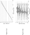
FIG. 3 shows the light vs. current and the spectral characteristics of the etched facet Fabry-Perot edge-emitting etched-facet laser with relatively small separation between adjacent lasers. -
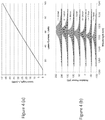
FIG. 4 shows the light vs. current and spectral characteristics of the etched facet Fabry-Perot laser with relatively large separation between adjacent lasers. -
FIG. 5 is a perspective view of edge-emitting etched-facet lasers according to the present invention. -
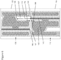
FIG. 6 is a top plan view of two adjacent edge-emitting etched-facet lasers according to the present invention similar toFIG. 5 . -
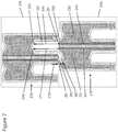
FIG. 7 is a top plan view of adjacent edge-emitting dual-cavity etched-facet DFB lasers according to the present invention. -
FIG. 8 is a top plan view of edge-emitting etched-facet lasers with laser chips offset from each other in each row of lasers. -
Fig. 1 shows a perspective view of asubstrate 90 with an epitaxially deposited waveguide structure including anactive region 80 in which etched-facet lasers including aridge 40 are fabricated. The etched-facetridge laser mesas front facet 50 of laser corresponding tomesa 10 is at adistance 70 from the back facet of laser corresponding tomesa 20. -
Fig. 2 shows a top plan view of two adjacent etched-facet ridge lasers, similar to those inFig. 1 . A wire-bond pad 30 is provided to allow wire-bonding to the pad and for electric current to be directed to the ridge allowing the laser to operate. Thelaser mesas chip chips Fig. 2 . - The
substrate 90 may be formed, for example, of a type III-V compound, or an alloy thereof, which may be suitably doped. The substrate, such as InP, includes a top surface on which is deposited, as by an epitaxial deposition such as Metalorganic Chemical Vapor Deposition (MOCVD) or Molecular Beam Epitaxy (MBE), a succession of layers which form an optical waveguide that includes anactive region 80. The semiconductor laser structure may contain upper and lower cladding regions, formed from lower index semiconductor material than theactive region 80, such as InP, adjacent theactive region 80, which may be formed with InAIGaAs-based quantum wells and barriers. The lower cladding may be formed partially through the epitaxial deposition and partly by using the substrate. For example, a 1310nm emitting epitaxial structure can be used with the following layers on an InP substrate 90: 0.5µm n-InP; 0.105 µm AlGaInAs lower graded region; anactive region 80 containing five 6nm thick compressively strained AlGaInAs quantum wells, each sandwiched by 10nm tensile strained AlGaInAs barriers; 0.105 µm AlGaInAs upper graded region; 1.65 µm thick p-InP upper cladding; and highly p-doped InGaAs cap layer. The structure may also have a wet etch stop layer. - One of the key benefits of etched-facet lasers is that testing is performed at wafer-level as opposed to bar-level testing for cleaved-facet lasers. However, to allow the full benefit of on-wafer testing, the
distance 70 has to be large enough to prevent the adverse impact of back-reflection and interference from back-facet 60 tofront facet 50. Thefront facet 50 is where most of the light emerges from the edge-emitting laser corresponding tomesa 10. For example, if thedistance 70 is 50 µm for an InP-based 1310nm Fabry-Perot (FP) ridge laser of ridge width of about 2 µm, the undesirable characteristics due to the back-reflection are observed inFigures 3 , whereFig. 3 (a) shows the laser Light vs. Current (or LI) characteristics starts to change at around 50 mA and a corresponding problem shows up inFig. 3 (b) above 50mA: the spectral characteristics of the laser have an abnormal double distribution of FP modes at currents above 50mA. Each spectrum is offset inFig. 3 (b) for clarity. - By increasing the
distance 70 to 100 µm or more for the 2 µm ridge width 1310nm FP lasers, the impact from the back-reflection and interference is minimized and the adverse impact is no longer seen in the LI characteristics ofFig. 4 (a) and the spectrum ofFig. 4(b) , where each spectrum is offset for clarity. The spectral results inFig. 4 (b) show a normal distribution for the FP modes. Thedistance 70 is also very important in on-wafer-testing of distributed feedback (DFB) lasers, wherein a grating is incorporated in the epitaxial structure. If thedistance 70 is too small, back-reflection can cause a change in the characteristics of the DFB laser and as a result the laser characteristics obtained after singulation may be different, significantly reducing the value of on-wafer testing. By choosing adistance 70 of 100µm or more, the undesirable impact of the back-reflection has been eliminated for 1310nm DFB lasers. However, increasing thedistance 70 to 100 µm or more is the wasted space that significantly reduces the number of chips that can be obtained from a wafer -
Fig. 5 shows a perspective view of asubstrate 190 with an epitaxially deposited structure, similar to the one described above, including anactive region 180 in which etched-facet lasers including aridge 140 are fabricated. The etched-facet lasers are arranged on the substrate in an alternating fashion front-to-back and back-to-front so that the planes of the front and back facets of two neighboring laser mesas face each other (and correspondingly, the planes of the back and front facets of two neighboring laser mesas face each other). In this arrangement, theetched ridge 140 oflaser mesa 110 is aligned withrecess 157 that is formed in neighboringlaser mesa 120. The etched-facetridge laser mesas front facet 150 of laser corresponding tomesa 110 is at adistance 170 from thewall 155 of the recessedregion 157. Thewall 155 can be at an angle other than normal to the incident laser beam to minimize back-reflection to thefront facet 150. The recessed region is around 5 µm deep, so that thewall 155 is around 5 µm in height and the floor of the recessed region is about 2.9 µm below the plane of the active region. In the case where thewall 155 is at an angle other than the normal, thedistance 170 can be reduced down from 100 µm, while avoiding the back-reflection and interference at levels that are detrimental to on-wafer testing. -
Fig. 6 illustrates a top plan view of two adjacent edge-emitting etched-facet lasers, similar toFIG. 5 . In practice, the two adjacent edge-emitting lasers ofFig. 6 are used as a unit building block and placed on the wafer in rows and columns. Theback facet 160 of laser corresponding tomesa 120 is high reflectivity coated, and as such, the impact of back-reflection is not too great. Nevertheless, a recessedregion 167 can be provided for minimizing back-reflection. Thewall 165 of the recessedregion 167 can also be at an angle other than normal to the incident laser beam to minimize back-reflection to theback facet 160. The laser mesas 110 and 120 are positioned onchip chips Fig. 6 . Thechip 115 including a wire-bond pad 130. Theseparation 175 betweenlaser mesas separation 175 has allowed a significantly larger number of laser chips to be produced from the same size wafer. Further, the recessedregions -
Fig. 7 shows the application of the present invention to the case of two laser cavities per chip. The laser mesas 210 and 220 are positioned onchip chips Fig. 7 . Thechip 215 comprises twolaser ridge cavities bond pads ridges Ridge laser 240 has afront facet 250 andridge laser 241 has afront facet 251. The adjacent mesa has a recessedregion 257 in front offacets walls facets distance 270 between thefront facet 250 and thewall 255 is preferably more than 100 µm, but could be shorter if the wall is at an angle to the normal of the laser beam emerging fromfacet 250. Similarly, thedistance 271 between thefront facet 251 and thewall 256 is preferably more than 100 µm, but could be shorter if the wall is at an angle to the normal of the laser beam emerging fromfacet 251. This allows thelaser mesas minimal separation 275 to increase the number of chips that can be produced from a given wafer. Theback facets mesa 220 can also face a recessedregion 267 in themesa 210 to minimize back-reflection. - Another alternative according to the present invention is illustrated in
Fig. 8 , where the etched-facet edge-emittinglaser mesas chips ridge 340 and a wire-bond pad 330 to provide electrical current to the ridge, as illustrated for laser corresponding tomesa 310. The recessed region 357 is formed completely on one side of the etched-facet laser chip 320 extending the full length of the chip, forming a complete opening. In this way, the recessed region 357 extends to theback facet 355 of a laser corresponding tomesa 321. Theback facet 355 is usually normal to the emitted laser light that emerges fromfront facet 350. The distance 370 is the distance betweenfront facet 350 and backfacet 355.Laser mesas minimal separation 375 in the top-to-bottom direction, similar to that inFigs. 6 and7 ; however,laser mesas minimal separation 376 in the left-to-right direction. This further allows an increase in the number of chips that can be produced from a given wafer. The sides of chips are only aligned in left-to-right, as opposed to the chips inFigs. 6 and7 that are aligned in both left-to-right and top-to-bottom. The singulation needs to accommodate this fact, and for example, the singulation needs to occur in the left-to-right direction first, and then chips separated by top-to-bottom singulation. AlthoughFig. 8 and the above description are in terms of a single laser cavity per chip, it will be understood that the same approach would be applicable to two or more laser cavities per chips. - The current invention is described using a 1310nm emitting laser that is based on an InP substrate. However, a number of other different epitaxial structures based on InP, GaAs, and GaN substrates, for example, can benefit from this invention. Numerous examples of epitaxial structures including active layers on these exemplary substrates are available that emit, for example, wavelengths in the infrared and visible regions of the spectrum. Further, although an edge-emitting ridge laser having an etched ridge has been described, it will be understood that other types of etched-facet lasers, such as etched-facet Buried Heterostructure (BH) lasers, can be used.
- Although the present invention has been illustrated in terms of various embodiments, it will be understood that variations and modifications may be made without departing from the scope thereof as set out in the following claims. Further, it will be understood that the dimensions and proportions shown in the figures are not necessarily to scale, but are used to clearly illustrate the salient features of the structure and method.
Claims (13)
- A laser structure comprising:a substrate (190);an epitaxial structure on the substrate (190), the epitaxial structure including an active region (180) for generating light;a first waveguide formed in a first portion of the epitaxial structure, the first waveguide extending in a first direction and having a first front etched facet and a first back etched facet (160) that define a first edge-emitting ridge waveguide or buried heterostructure laser (120);a second waveguide (140) formed in a second portion of the epitaxial structure, displaced along the first direction relative to the first waveguide, the second waveguide (140) also being displaced in the lateral direction relative to the first waveguide, the second waveguide (140) extending in the first direction and having a second front etched facet (150) and a second back etched facet that define a second edge-emitting ridge waveguide or buried heterostructure laser (110); anda first recessed region (157) formed in said epitaxial structure, the first recessed region (157) being arranged at a first lateral distance from the first waveguide and having an opening adjacent to the first back etched facet (160) of the first waveguide and directly opposite the second front etched facet (150) of the second waveguide (140), such that light emitted from the second front etched facet (150) of the second waveguide (140) is incident into the first recessed region (157), and is not incident on the first back etched facet (160) of the first waveguide, the first recessed region thus facilitating testing of the second edge-emitting laser (110) prior to singulation of the laser structure into laser chips (115, 125).
- The laser structure of claim 1, wherein the first recessed region (157) has a first end wall (155).
- The laser structure of claim 2, wherein the light from the second front etched facet (150) of the second waveguide (140) impinges the first end wall (155) of the first recessed region (157).
- The laser structure of any preceding claim, further comprising:
a second recessed region (167, 267) formed in said first portion of said epitaxial structure and arranged at a second lateral distance from the first waveguide and having an opening adjacent to the first front etched facet (150, 250), the second recessed region (167, 267) including a second end wall (165). - The laser structure of claim 4, wherein the second recessed region (167, 267) facilitates testing of a second adjacent laser chip prior to singulation of the second adjacent laser chip from the substrate, by minimizing back-reflection.
- The laser structure of claim 3, wherein the first end wall (155) is at an angle other than normal to the first direction.
- The laser structure of claim 6, wherein the first back etched facet (160) and the second back etched facet are coated with a highly reflective material.
- The laser structure of claim 4 or claim 5, wherein the second end wall (165) is at an angle other than normal to the first direction.
- The laser structure of claim 8, wherein the opening to the first recessed region (157) and the opening to the second recessed region (167) are aligned to each other along the first direction.
- The laser structure of claim 1, wherein the ridge laser or the Buried Heterostructure (BH) laser is either:a Fabry-Perot (FP) type; ora distributed feedback (DFB) type.
- The laser structure of claim 1, wherein the substrate is InP, or wherein the substrate is GaAs, or wherein the substrate is GaN.
- A method of fabricating a semiconductor laser structure comprising:depositing an epitaxial structure on a substrate (190), the epitaxial structure including an active region (180) for generating light;forming first and second waveguides (140) along a first direction in first and second portions of the structure respectively, the second waveguide (140) being displaced relative to the first waveguide in the first direction and in the lateral direction,the first waveguide having a first front etched facet and a first back etched facet (160), the second waveguide (140) having a second front etched facet (150) and a second back etched facet, thereby defining first and second edge-emitting ridge waveguide or buried heterostructure lasers (120, 110) ;forming a recessed region (157) in the first portion of the structure, a lateral distance from the first waveguide, the recessed region having an opening adjacent to the first back etched facet (160) of the first waveguide and directly opposing the second front etched facet (150) of the second waveguide (140), the recessed region (157) facilitating testing of the second waveguide (140) rior to singulation of the laser structure by being arranged such that light emitted from the second front etched facet (150) of the second waveguide (140) is incident into the recessed region (157), and is not incident on the back etched facet (160) of the first waveguide.
- A method of testing semiconductor lasers comprising:
providing the laser structure of one of claims 1-11; and measuring laser light vs. current characteristics and/or spectral characteristics of the light emitted from the second front etched facet (150) of the second waveguide (140) at wafer level prior to singulation.
Applications Claiming Priority (4)
| Application Number | Priority Date | Filing Date | Title |
|---|---|---|---|
| US201161568383P | 2011-12-08 | 2011-12-08 | |
| US201261619190P | 2012-04-02 | 2012-04-02 | |
| US13/690,792 US8934512B2 (en) | 2011-12-08 | 2012-11-30 | Edge-emitting etched-facet lasers |
| PCT/US2012/067612 WO2013085845A1 (en) | 2011-12-08 | 2012-12-03 | Edge-emitting etched-facet lasers |
Publications (3)
| Publication Number | Publication Date |
|---|---|
| EP2789060A1 EP2789060A1 (en) | 2014-10-15 |
| EP2789060A4 EP2789060A4 (en) | 2015-11-11 |
| EP2789060B1 true EP2789060B1 (en) | 2021-05-19 |
Family
ID=48574793
Family Applications (1)
| Application Number | Title | Priority Date | Filing Date |
|---|---|---|---|
| EP12855851.7A Active EP2789060B1 (en) | 2011-12-08 | 2012-12-03 | Edge-emitting etched-facet lasers |
Country Status (5)
| Country | Link |
|---|---|
| US (4) | US8934512B2 (en) |
| EP (1) | EP2789060B1 (en) |
| JP (2) | JP6082021B2 (en) |
| CN (1) | CN104067462B (en) |
| WO (1) | WO2013085845A1 (en) |
Families Citing this family (20)
| Publication number | Priority date | Publication date | Assignee | Title |
|---|---|---|---|---|
| US8934512B2 (en) | 2011-12-08 | 2015-01-13 | Binoptics Corporation | Edge-emitting etched-facet lasers |
| KR102186432B1 (en) | 2014-03-25 | 2020-12-03 | 엘지전자 주식회사 | A plasma electrode device |
| DE102015115812B4 (en) * | 2015-09-18 | 2025-12-04 | OSRAM Opto Semiconductors Gesellschaft mit beschränkter Haftung | Component and method for manufacturing a component |
| DE102015116712B4 (en) * | 2015-10-01 | 2024-11-28 | OSRAM Opto Semiconductors Gesellschaft mit beschränkter Haftung | optoelectronic component |
| DE102016101942B4 (en) * | 2016-02-04 | 2022-07-21 | OSRAM Opto Semiconductors Gesellschaft mit beschränkter Haftung | Method for producing an optoelectronic lighting device |
| CN107706738B (en) * | 2016-08-09 | 2020-07-28 | 清华大学 | Distributed feedback semiconductor laser and preparation method thereof |
| CN106229808B (en) * | 2016-09-20 | 2023-08-29 | 中国电子科技集团公司第十三研究所 | pulsed laser |
| CN107872007B (en) * | 2016-09-27 | 2019-11-22 | 青岛海信宽带多媒体技术有限公司 | A method of manufacturing a laser chip |
| CN107611772B (en) * | 2017-09-25 | 2020-07-28 | 清华大学 | Electroabsorption modulated laser and preparation method thereof |
| CN108242763B (en) * | 2018-03-05 | 2020-02-18 | 中国科学院半导体研究所 | Monolithic structure of electro-absorption modulated laser and its fabrication and testing method |
| CN108718032A (en) * | 2018-05-18 | 2018-10-30 | 河南仕佳光子科技股份有限公司 | A kind of method that full wafer makes and tests edge emitting optical device |
| WO2020106974A1 (en) | 2018-11-21 | 2020-05-28 | Skorpios Technologies, Inc. | Etched facet in a multi quantum well structure |
| KR102068188B1 (en) * | 2018-11-26 | 2020-02-18 | 주식회사 오이솔루션 | Laser device and manufacturing method thereof |
| CN111029905A (en) * | 2019-11-29 | 2020-04-17 | 河南仕佳光子科技股份有限公司 | Typesetting structure for integrally manufacturing edge-emitting optical device |
| CN111129945B (en) * | 2019-11-29 | 2021-06-18 | 河南仕佳光子科技股份有限公司 | Method for integrally manufacturing isolator-saving edge-emitting laser chip |
| CN111082311B (en) * | 2019-12-31 | 2022-04-01 | 中国科学院半导体研究所 | Monolithic manufacturing structure of monolithic photonic integrated device |
| US11226457B2 (en) | 2020-05-28 | 2022-01-18 | Cisco Technology, Inc. | Laser and photonic chip integration |
| DE102021103484A1 (en) * | 2021-02-15 | 2022-08-18 | OSRAM Opto Semiconductors Gesellschaft mit beschränkter Haftung | PROCESSES FOR MANUFACTURING A VARIETY OF SEMICONDUCTOR LASERS AND SEMICONDUCTOR LASERS |
| US20240106200A1 (en) * | 2022-09-27 | 2024-03-28 | Lumentum Operations Llc | Optical device that includes an epitaxial layer structure with trenches and grooves |
| WO2026003907A1 (en) * | 2024-06-24 | 2026-01-02 | Ntt株式会社 | Method for manufacturing semiconductor device |
Family Cites Families (28)
| Publication number | Priority date | Publication date | Assignee | Title |
|---|---|---|---|---|
| JPS62102582A (en) * | 1985-10-29 | 1987-05-13 | Seiko Epson Corp | Inspecting method for semiconductor laser |
| US4851368A (en) | 1987-12-04 | 1989-07-25 | Cornell Research Foundation, Inc. | Method of making travelling wave semi-conductor laser |
| EP0410067B1 (en) * | 1989-07-27 | 1993-09-22 | International Business Machines Corporation | Integrated semiconductor diode laser and photodiode structure |
| JPH04340286A (en) * | 1991-02-07 | 1992-11-26 | Nec Corp | Manufacture of semiconductor laser |
| JPH04280492A (en) * | 1991-03-07 | 1992-10-06 | Toshiba Corp | Manufacture of optical semiconductor element |
| US5258991A (en) * | 1992-03-13 | 1993-11-02 | Eastman Kodak Company | Monolithic laser diode and monitor photodetector |
| JPH0637402A (en) * | 1992-07-20 | 1994-02-10 | Nippon Telegr & Teleph Corp <Ntt> | Semiconductor laser light reflection element |
| JPH09216409A (en) * | 1996-02-08 | 1997-08-19 | Fuji Xerox Co Ltd | Light source unit and optical scanner using end-face luminescent semiconductor laser element |
| JP2000312054A (en) | 1998-04-28 | 2000-11-07 | Sharp Corp | Method of manufacturing semiconductor element and semiconductor element |
| US6668000B2 (en) * | 1999-07-15 | 2003-12-23 | University Of Maryland, Baltimore County | System and method of optically testing multiple edge-emitting semiconductor lasers residing on a common wafer |
| JP2002111128A (en) * | 2000-07-28 | 2002-04-12 | Nichia Chem Ind Ltd | Semiconductor laser device and method for forming the same |
| JP4026334B2 (en) * | 2001-07-30 | 2007-12-26 | 株式会社日立製作所 | Semiconductor laser, distributed feedback semiconductor laser, and wavelength tunable semiconductor laser |
| EP1309050A1 (en) | 2001-11-06 | 2003-05-07 | Agilent Technologies, Inc. (a Delaware corporation) | Laser device and method therefor |
| GB2387479A (en) * | 2002-04-08 | 2003-10-15 | Denselight Semiconductors Pte | Sacrificial side tilting mirror for on-wafer optical testing |
| NL1023767C1 (en) * | 2003-06-27 | 2004-12-28 | Clea Technologies B V | Process for separating optical isomers from a protected amino acid. |
| WO2005011076A1 (en) | 2003-07-31 | 2005-02-03 | Bookham Technology Plc | Weakly guiding ridge waveguides with vertical gratings |
| JP4696522B2 (en) * | 2003-10-14 | 2011-06-08 | 日亜化学工業株式会社 | Semiconductor laser element |
| US7440666B2 (en) | 2004-02-25 | 2008-10-21 | Avago Technologies Fiber Ip (Singapore) Pte. Ltd. | Buried heterostucture device having integrated waveguide grating fabricated by single step MOCVD |
| US8787419B2 (en) * | 2005-02-18 | 2014-07-22 | Binoptics Corporation | High reliability etched-facet photonic devices |
| EP2797185B1 (en) * | 2005-06-22 | 2018-09-05 | MACOM Technology Solutions Holdings, Inc. | AIGalnN-based lasers produced using etched facet technology |
| CN102035135B (en) | 2005-08-25 | 2013-02-27 | 宾奥普迪克斯股份有限公司 | Semiconductor laser resonator formed on single sheet |
| US20070047609A1 (en) * | 2005-08-30 | 2007-03-01 | Francis Daniel A | Wafer testing of edge emitting lasers |
| US7606277B2 (en) * | 2006-12-26 | 2009-10-20 | Binoptics Corporation | Etched-facet ridge lasers with etch-stop |
| JP2009135305A (en) * | 2007-11-30 | 2009-06-18 | Anritsu Corp | Light-emitting element wafer, light-emitting element chip, burn-in method, and manufacturing method of light-emitting element chip |
| US8064493B2 (en) | 2009-06-12 | 2011-11-22 | Binoptics Corporation | Surface emitting photonic device |
| EP2454787B1 (en) * | 2009-07-13 | 2018-02-28 | Oclaro Technology Limited | Integrated photodiode wavelength monitor |
| JP2011192728A (en) * | 2010-03-12 | 2011-09-29 | Renesas Electronics Corp | Method of manufacturing semiconductor laser |
| US8934512B2 (en) | 2011-12-08 | 2015-01-13 | Binoptics Corporation | Edge-emitting etched-facet lasers |
-
2012
- 2012-11-30 US US13/690,792 patent/US8934512B2/en active Active
- 2012-12-03 JP JP2014545967A patent/JP6082021B2/en active Active
- 2012-12-03 WO PCT/US2012/067612 patent/WO2013085845A1/en not_active Ceased
- 2012-12-03 CN CN201280067696.9A patent/CN104067462B/en active Active
- 2012-12-03 EP EP12855851.7A patent/EP2789060B1/en active Active
-
2015
- 2015-01-13 US US14/595,848 patent/US9893488B2/en active Active
-
2016
- 2016-06-30 JP JP2016129819A patent/JP6258414B2/en active Active
-
2017
- 2017-12-01 US US15/829,133 patent/US10044168B2/en active Active
- 2017-12-01 US US15/829,151 patent/US10038298B2/en active Active
Non-Patent Citations (1)
| Title |
|---|
| None * |
Also Published As
| Publication number | Publication date |
|---|---|
| US10044168B2 (en) | 2018-08-07 |
| US8934512B2 (en) | 2015-01-13 |
| JP2016208040A (en) | 2016-12-08 |
| US9893488B2 (en) | 2018-02-13 |
| US20180090907A1 (en) | 2018-03-29 |
| US20180109070A1 (en) | 2018-04-19 |
| JP6082021B2 (en) | 2017-02-15 |
| CN104067462A (en) | 2014-09-24 |
| EP2789060A1 (en) | 2014-10-15 |
| JP2015502052A (en) | 2015-01-19 |
| US20150123695A1 (en) | 2015-05-07 |
| US10038298B2 (en) | 2018-07-31 |
| US20130156059A1 (en) | 2013-06-20 |
| CN104067462B (en) | 2017-09-08 |
| WO2013085845A1 (en) | 2013-06-13 |
| EP2789060A4 (en) | 2015-11-11 |
| JP6258414B2 (en) | 2018-01-10 |
Similar Documents
| Publication | Publication Date | Title |
|---|---|---|
| US10038298B2 (en) | Edge-emitting etched-facet lasers | |
| US8419956B2 (en) | Surface emitting photonic device | |
| US9865993B2 (en) | Lasers with beam-shape modification | |
| US8306086B2 (en) | Algainn-based lasers produced using etched facet technology | |
| US8442084B2 (en) | High performance vertically emitting lasers | |
| Lammert et al. | Low-threshold narrow-linewidth InGaAs-GaAs ridge-waveguide DBR lasers with first-order surface gratings | |
| Kyaw | Quantum dots based superluminescent diodes and photonic crystal surface emitting lasers |
Legal Events
| Date | Code | Title | Description |
|---|---|---|---|
| PUAI | Public reference made under article 153(3) epc to a published international application that has entered the european phase |
Free format text: ORIGINAL CODE: 0009012 |
|
| 17P | Request for examination filed |
Effective date: 20140704 |
|
| AK | Designated contracting states |
Kind code of ref document: A1 Designated state(s): AL AT BE BG CH CY CZ DE DK EE ES FI FR GB GR HR HU IE IS IT LI LT LU LV MC MK MT NL NO PL PT RO RS SE SI SK SM TR |
|
| DAX | Request for extension of the european patent (deleted) | ||
| RA4 | Supplementary search report drawn up and despatched (corrected) |
Effective date: 20151009 |
|
| RIC1 | Information provided on ipc code assigned before grant |
Ipc: H01S 5/00 20060101AFI20151005BHEP Ipc: H01S 5/22 20060101ALN20151005BHEP Ipc: G01R 31/26 20140101ALN20151005BHEP Ipc: H01S 5/02 20060101ALN20151005BHEP Ipc: H01S 5/028 20060101ALN20151005BHEP |
|
| RAP1 | Party data changed (applicant data changed or rights of an application transferred) |
Owner name: M/A-COM TECHNOLOGY SOLUTIONS HOLDINGS, INC. |
|
| RAP1 | Party data changed (applicant data changed or rights of an application transferred) |
Owner name: MACOM TECHNOLOGY SOLUTIONS HOLDINGS, INC. |
|
| STAA | Information on the status of an ep patent application or granted ep patent |
Free format text: STATUS: EXAMINATION IS IN PROGRESS |
|
| 17Q | First examination report despatched |
Effective date: 20171113 |
|
| RIC1 | Information provided on ipc code assigned before grant |
Ipc: H01S 5/00 20060101AFI20201012BHEP Ipc: H01S 5/22 20060101ALN20201012BHEP Ipc: H01S 5/02 20060101ALN20201012BHEP Ipc: H01S 5/028 20060101ALN20201012BHEP Ipc: G01R 31/26 20200101ALN20201012BHEP |
|
| RIC1 | Information provided on ipc code assigned before grant |
Ipc: H01S 5/02 20060101ALN20201104BHEP Ipc: G01R 31/26 20200101ALN20201104BHEP Ipc: H01S 5/22 20060101ALN20201104BHEP Ipc: H01S 5/028 20060101ALN20201104BHEP Ipc: H01S 5/00 20060101AFI20201104BHEP |
|
| GRAP | Despatch of communication of intention to grant a patent |
Free format text: ORIGINAL CODE: EPIDOSNIGR1 |
|
| STAA | Information on the status of an ep patent application or granted ep patent |
Free format text: STATUS: GRANT OF PATENT IS INTENDED |
|
| RIC1 | Information provided on ipc code assigned before grant |
Ipc: H01S 5/22 20060101ALN20201116BHEP Ipc: H01S 5/00 20060101AFI20201116BHEP Ipc: H01S 5/028 20060101ALN20201116BHEP Ipc: H01S 5/02 20060101ALN20201116BHEP Ipc: G01R 31/26 20200101ALN20201116BHEP |
|
| INTG | Intention to grant announced |
Effective date: 20201215 |
|
| GRAS | Grant fee paid |
Free format text: ORIGINAL CODE: EPIDOSNIGR3 |
|
| GRAA | (expected) grant |
Free format text: ORIGINAL CODE: 0009210 |
|
| STAA | Information on the status of an ep patent application or granted ep patent |
Free format text: STATUS: THE PATENT HAS BEEN GRANTED |
|
| AK | Designated contracting states |
Kind code of ref document: B1 Designated state(s): AL AT BE BG CH CY CZ DE DK EE ES FI FR GB GR HR HU IE IS IT LI LT LU LV MC MK MT NL NO PL PT RO RS SE SI SK SM TR |
|
| REG | Reference to a national code |
Ref country code: GB Ref legal event code: FG4D |
|
| REG | Reference to a national code |
Ref country code: CH Ref legal event code: EP |
|
| REG | Reference to a national code |
Ref country code: DE Ref legal event code: R096 Ref document number: 602012075634 Country of ref document: DE |
|
| REG | Reference to a national code |
Ref country code: AT Ref legal event code: REF Ref document number: 1394908 Country of ref document: AT Kind code of ref document: T Effective date: 20210615 |
|
| REG | Reference to a national code |
Ref country code: IE Ref legal event code: FG4D |
|
| REG | Reference to a national code |
Ref country code: LT Ref legal event code: MG9D |
|
| REG | Reference to a national code |
Ref country code: AT Ref legal event code: MK05 Ref document number: 1394908 Country of ref document: AT Kind code of ref document: T Effective date: 20210519 |
|
| REG | Reference to a national code |
Ref country code: NL Ref legal event code: MP Effective date: 20210519 |
|
| PG25 | Lapsed in a contracting state [announced via postgrant information from national office to epo] |
Ref country code: BG Free format text: LAPSE BECAUSE OF FAILURE TO SUBMIT A TRANSLATION OF THE DESCRIPTION OR TO PAY THE FEE WITHIN THE PRESCRIBED TIME-LIMIT Effective date: 20210819 Ref country code: AT Free format text: LAPSE BECAUSE OF FAILURE TO SUBMIT A TRANSLATION OF THE DESCRIPTION OR TO PAY THE FEE WITHIN THE PRESCRIBED TIME-LIMIT Effective date: 20210519 Ref country code: HR Free format text: LAPSE BECAUSE OF FAILURE TO SUBMIT A TRANSLATION OF THE DESCRIPTION OR TO PAY THE FEE WITHIN THE PRESCRIBED TIME-LIMIT Effective date: 20210519 Ref country code: FI Free format text: LAPSE BECAUSE OF FAILURE TO SUBMIT A TRANSLATION OF THE DESCRIPTION OR TO PAY THE FEE WITHIN THE PRESCRIBED TIME-LIMIT Effective date: 20210519 Ref country code: LT Free format text: LAPSE BECAUSE OF FAILURE TO SUBMIT A TRANSLATION OF THE DESCRIPTION OR TO PAY THE FEE WITHIN THE PRESCRIBED TIME-LIMIT Effective date: 20210519 |
|
| PG25 | Lapsed in a contracting state [announced via postgrant information from national office to epo] |
Ref country code: GR Free format text: LAPSE BECAUSE OF FAILURE TO SUBMIT A TRANSLATION OF THE DESCRIPTION OR TO PAY THE FEE WITHIN THE PRESCRIBED TIME-LIMIT Effective date: 20210820 Ref country code: LV Free format text: LAPSE BECAUSE OF FAILURE TO SUBMIT A TRANSLATION OF THE DESCRIPTION OR TO PAY THE FEE WITHIN THE PRESCRIBED TIME-LIMIT Effective date: 20210519 Ref country code: IS Free format text: LAPSE BECAUSE OF FAILURE TO SUBMIT A TRANSLATION OF THE DESCRIPTION OR TO PAY THE FEE WITHIN THE PRESCRIBED TIME-LIMIT Effective date: 20210919 Ref country code: SE Free format text: LAPSE BECAUSE OF FAILURE TO SUBMIT A TRANSLATION OF THE DESCRIPTION OR TO PAY THE FEE WITHIN THE PRESCRIBED TIME-LIMIT Effective date: 20210519 Ref country code: RS Free format text: LAPSE BECAUSE OF FAILURE TO SUBMIT A TRANSLATION OF THE DESCRIPTION OR TO PAY THE FEE WITHIN THE PRESCRIBED TIME-LIMIT Effective date: 20210519 Ref country code: NO Free format text: LAPSE BECAUSE OF FAILURE TO SUBMIT A TRANSLATION OF THE DESCRIPTION OR TO PAY THE FEE WITHIN THE PRESCRIBED TIME-LIMIT Effective date: 20210819 Ref country code: PT Free format text: LAPSE BECAUSE OF FAILURE TO SUBMIT A TRANSLATION OF THE DESCRIPTION OR TO PAY THE FEE WITHIN THE PRESCRIBED TIME-LIMIT Effective date: 20210920 Ref country code: PL Free format text: LAPSE BECAUSE OF FAILURE TO SUBMIT A TRANSLATION OF THE DESCRIPTION OR TO PAY THE FEE WITHIN THE PRESCRIBED TIME-LIMIT Effective date: 20210519 Ref country code: ES Free format text: LAPSE BECAUSE OF FAILURE TO SUBMIT A TRANSLATION OF THE DESCRIPTION OR TO PAY THE FEE WITHIN THE PRESCRIBED TIME-LIMIT Effective date: 20210519 |
|
| PG25 | Lapsed in a contracting state [announced via postgrant information from national office to epo] |
Ref country code: NL Free format text: LAPSE BECAUSE OF FAILURE TO SUBMIT A TRANSLATION OF THE DESCRIPTION OR TO PAY THE FEE WITHIN THE PRESCRIBED TIME-LIMIT Effective date: 20210519 |
|
| PG25 | Lapsed in a contracting state [announced via postgrant information from national office to epo] |
Ref country code: RO Free format text: LAPSE BECAUSE OF FAILURE TO SUBMIT A TRANSLATION OF THE DESCRIPTION OR TO PAY THE FEE WITHIN THE PRESCRIBED TIME-LIMIT Effective date: 20210519 Ref country code: EE Free format text: LAPSE BECAUSE OF FAILURE TO SUBMIT A TRANSLATION OF THE DESCRIPTION OR TO PAY THE FEE WITHIN THE PRESCRIBED TIME-LIMIT Effective date: 20210519 Ref country code: DK Free format text: LAPSE BECAUSE OF FAILURE TO SUBMIT A TRANSLATION OF THE DESCRIPTION OR TO PAY THE FEE WITHIN THE PRESCRIBED TIME-LIMIT Effective date: 20210519 Ref country code: CZ Free format text: LAPSE BECAUSE OF FAILURE TO SUBMIT A TRANSLATION OF THE DESCRIPTION OR TO PAY THE FEE WITHIN THE PRESCRIBED TIME-LIMIT Effective date: 20210519 Ref country code: SM Free format text: LAPSE BECAUSE OF FAILURE TO SUBMIT A TRANSLATION OF THE DESCRIPTION OR TO PAY THE FEE WITHIN THE PRESCRIBED TIME-LIMIT Effective date: 20210519 Ref country code: SK Free format text: LAPSE BECAUSE OF FAILURE TO SUBMIT A TRANSLATION OF THE DESCRIPTION OR TO PAY THE FEE WITHIN THE PRESCRIBED TIME-LIMIT Effective date: 20210519 |
|
| REG | Reference to a national code |
Ref country code: DE Ref legal event code: R097 Ref document number: 602012075634 Country of ref document: DE |
|
| PLBE | No opposition filed within time limit |
Free format text: ORIGINAL CODE: 0009261 |
|
| STAA | Information on the status of an ep patent application or granted ep patent |
Free format text: STATUS: NO OPPOSITION FILED WITHIN TIME LIMIT |
|
| 26N | No opposition filed |
Effective date: 20220222 |
|
| PG25 | Lapsed in a contracting state [announced via postgrant information from national office to epo] |
Ref country code: IS Free format text: LAPSE BECAUSE OF FAILURE TO SUBMIT A TRANSLATION OF THE DESCRIPTION OR TO PAY THE FEE WITHIN THE PRESCRIBED TIME-LIMIT Effective date: 20210919 Ref country code: AL Free format text: LAPSE BECAUSE OF FAILURE TO SUBMIT A TRANSLATION OF THE DESCRIPTION OR TO PAY THE FEE WITHIN THE PRESCRIBED TIME-LIMIT Effective date: 20210519 |
|
| PG25 | Lapsed in a contracting state [announced via postgrant information from national office to epo] |
Ref country code: MC Free format text: LAPSE BECAUSE OF FAILURE TO SUBMIT A TRANSLATION OF THE DESCRIPTION OR TO PAY THE FEE WITHIN THE PRESCRIBED TIME-LIMIT Effective date: 20210519 |
|
| REG | Reference to a national code |
Ref country code: CH Ref legal event code: PL |
|
| GBPC | Gb: european patent ceased through non-payment of renewal fee |
Effective date: 20211203 |
|
| REG | Reference to a national code |
Ref country code: BE Ref legal event code: MM Effective date: 20211231 |
|
| PG25 | Lapsed in a contracting state [announced via postgrant information from national office to epo] |
Ref country code: LU Free format text: LAPSE BECAUSE OF NON-PAYMENT OF DUE FEES Effective date: 20211203 Ref country code: IE Free format text: LAPSE BECAUSE OF NON-PAYMENT OF DUE FEES Effective date: 20211203 Ref country code: GB Free format text: LAPSE BECAUSE OF NON-PAYMENT OF DUE FEES Effective date: 20211203 |
|
| PG25 | Lapsed in a contracting state [announced via postgrant information from national office to epo] |
Ref country code: BE Free format text: LAPSE BECAUSE OF NON-PAYMENT OF DUE FEES Effective date: 20211231 |
|
| PG25 | Lapsed in a contracting state [announced via postgrant information from national office to epo] |
Ref country code: LI Free format text: LAPSE BECAUSE OF NON-PAYMENT OF DUE FEES Effective date: 20211231 Ref country code: CH Free format text: LAPSE BECAUSE OF NON-PAYMENT OF DUE FEES Effective date: 20211231 |
|
| PG25 | Lapsed in a contracting state [announced via postgrant information from national office to epo] |
Ref country code: HU Free format text: LAPSE BECAUSE OF FAILURE TO SUBMIT A TRANSLATION OF THE DESCRIPTION OR TO PAY THE FEE WITHIN THE PRESCRIBED TIME-LIMIT; INVALID AB INITIO Effective date: 20121203 Ref country code: CY Free format text: LAPSE BECAUSE OF FAILURE TO SUBMIT A TRANSLATION OF THE DESCRIPTION OR TO PAY THE FEE WITHIN THE PRESCRIBED TIME-LIMIT Effective date: 20210519 |
|
| P01 | Opt-out of the competence of the unified patent court (upc) registered |
Effective date: 20230530 |
|
| PG25 | Lapsed in a contracting state [announced via postgrant information from national office to epo] |
Ref country code: MK Free format text: LAPSE BECAUSE OF FAILURE TO SUBMIT A TRANSLATION OF THE DESCRIPTION OR TO PAY THE FEE WITHIN THE PRESCRIBED TIME-LIMIT Effective date: 20210519 |
|
| PG25 | Lapsed in a contracting state [announced via postgrant information from national office to epo] |
Ref country code: MT Free format text: LAPSE BECAUSE OF FAILURE TO SUBMIT A TRANSLATION OF THE DESCRIPTION OR TO PAY THE FEE WITHIN THE PRESCRIBED TIME-LIMIT Effective date: 20210519 |
|
| PG25 | Lapsed in a contracting state [announced via postgrant information from national office to epo] |
Ref country code: TR Free format text: LAPSE BECAUSE OF FAILURE TO SUBMIT A TRANSLATION OF THE DESCRIPTION OR TO PAY THE FEE WITHIN THE PRESCRIBED TIME-LIMIT Effective date: 20210519 |
|
| PGFP | Annual fee paid to national office [announced via postgrant information from national office to epo] |
Ref country code: IT Payment date: 20251218 Year of fee payment: 14 |
|
| PGFP | Annual fee paid to national office [announced via postgrant information from national office to epo] |
Ref country code: FR Payment date: 20251230 Year of fee payment: 14 |
|
| PGFP | Annual fee paid to national office [announced via postgrant information from national office to epo] |
Ref country code: DE Payment date: 20251229 Year of fee payment: 14 |