EP2786437B1 - Organic light emitting ambipolar field effect transistor with distributed light emission - Google Patents
Organic light emitting ambipolar field effect transistor with distributed light emission Download PDFInfo
- Publication number
- EP2786437B1 EP2786437B1 EP13716411.7A EP13716411A EP2786437B1 EP 2786437 B1 EP2786437 B1 EP 2786437B1 EP 13716411 A EP13716411 A EP 13716411A EP 2786437 B1 EP2786437 B1 EP 2786437B1
- Authority
- EP
- European Patent Office
- Prior art keywords
- lumo
- homo
- comprised
- scn
- difference
- Prior art date
- Legal status (The legal status is an assumption and is not a legal conclusion. Google has not performed a legal analysis and makes no representation as to the accuracy of the status listed.)
- Not-in-force
Links
Images


Classifications
-
- H—ELECTRICITY
- H10—SEMICONDUCTOR DEVICES; ELECTRIC SOLID-STATE DEVICES NOT OTHERWISE PROVIDED FOR
- H10K—ORGANIC ELECTRIC SOLID-STATE DEVICES
- H10K50/00—Organic light-emitting devices
- H10K50/10—OLEDs or polymer light-emitting diodes [PLED]
- H10K50/11—OLEDs or polymer light-emitting diodes [PLED] characterised by the electroluminescent [EL] layers
- H10K50/12—OLEDs or polymer light-emitting diodes [PLED] characterised by the electroluminescent [EL] layers comprising dopants
-
- H—ELECTRICITY
- H10—SEMICONDUCTOR DEVICES; ELECTRIC SOLID-STATE DEVICES NOT OTHERWISE PROVIDED FOR
- H10K—ORGANIC ELECTRIC SOLID-STATE DEVICES
- H10K50/00—Organic light-emitting devices
- H10K50/30—Organic light-emitting transistors
-
- H—ELECTRICITY
- H10—SEMICONDUCTOR DEVICES; ELECTRIC SOLID-STATE DEVICES NOT OTHERWISE PROVIDED FOR
- H10K—ORGANIC ELECTRIC SOLID-STATE DEVICES
- H10K50/00—Organic light-emitting devices
- H10K50/80—Constructional details
- H10K50/805—Electrodes
-
- H—ELECTRICITY
- H10—SEMICONDUCTOR DEVICES; ELECTRIC SOLID-STATE DEVICES NOT OTHERWISE PROVIDED FOR
- H10K—ORGANIC ELECTRIC SOLID-STATE DEVICES
- H10K2101/00—Properties of the organic materials covered by group H10K85/00
- H10K2101/30—Highest occupied molecular orbital [HOMO], lowest unoccupied molecular orbital [LUMO] or Fermi energy values
-
- H—ELECTRICITY
- H10—SEMICONDUCTOR DEVICES; ELECTRIC SOLID-STATE DEVICES NOT OTHERWISE PROVIDED FOR
- H10K—ORGANIC ELECTRIC SOLID-STATE DEVICES
- H10K2101/00—Properties of the organic materials covered by group H10K85/00
- H10K2101/40—Interrelation of parameters between multiple constituent active layers or sublayers, e.g. HOMO values in adjacent layers
-
- H—ELECTRICITY
- H10—SEMICONDUCTOR DEVICES; ELECTRIC SOLID-STATE DEVICES NOT OTHERWISE PROVIDED FOR
- H10K—ORGANIC ELECTRIC SOLID-STATE DEVICES
- H10K71/00—Manufacture or treatment specially adapted for the organic devices covered by this subclass
- H10K71/311—Purifying organic semiconductor materials
-
- H—ELECTRICITY
- H10—SEMICONDUCTOR DEVICES; ELECTRIC SOLID-STATE DEVICES NOT OTHERWISE PROVIDED FOR
- H10K—ORGANIC ELECTRIC SOLID-STATE DEVICES
- H10K85/00—Organic materials used in the body or electrodes of devices covered by this subclass
- H10K85/30—Coordination compounds
- H10K85/321—Metal complexes comprising a group IIIA element, e.g. Tris (8-hydroxyquinoline) gallium [Gaq3]
- H10K85/324—Metal complexes comprising a group IIIA element, e.g. Tris (8-hydroxyquinoline) gallium [Gaq3] comprising aluminium, e.g. Alq3
-
- H—ELECTRICITY
- H10—SEMICONDUCTOR DEVICES; ELECTRIC SOLID-STATE DEVICES NOT OTHERWISE PROVIDED FOR
- H10K—ORGANIC ELECTRIC SOLID-STATE DEVICES
- H10K85/00—Organic materials used in the body or electrodes of devices covered by this subclass
- H10K85/30—Coordination compounds
- H10K85/341—Transition metal complexes, e.g. Ru(II)polypyridine complexes
- H10K85/346—Transition metal complexes, e.g. Ru(II)polypyridine complexes comprising platinum
-
- H—ELECTRICITY
- H10—SEMICONDUCTOR DEVICES; ELECTRIC SOLID-STATE DEVICES NOT OTHERWISE PROVIDED FOR
- H10K—ORGANIC ELECTRIC SOLID-STATE DEVICES
- H10K85/00—Organic materials used in the body or electrodes of devices covered by this subclass
- H10K85/60—Organic compounds having low molecular weight
- H10K85/649—Aromatic compounds comprising a hetero atom
- H10K85/655—Aromatic compounds comprising a hetero atom comprising only sulfur as heteroatom
Definitions
- This invention relates to an organic light emitting field effect transistor with distributed light emission.
- the term distributed light emission refers to a light emission by a length greater than or equal to 20 ⁇ m.
- OLET Organic electroluminescent field effect transistors
- OLED Organic Light Emitting Diodes
- ambipolar OLET have enhanced efficiency and luminosity, and also the possibility of using low cost production processes, once they have been optimized.
- This spatially confined emission does not cause problems in a whole class of organic-electronic devices, and it may be an advantage, for example in the field of sensing devices.
- This use is described for example in the international patent application WO2010049871 . Nevertheless, this limits the possible application fields when a large or distributed source of light is needed, such as for example in the field of ambient lighting, of electroluminescent display technology, of the so-called Point of Care biomedical applications, of light sources with high brightness integrated on photonic chips.
- An objective of the present invention is thus to overcome the problems of prior art, making reference to the limited extension of the illuminated region of a field effect transistor, and according to a first aspect it consists in an organic ambipolar light emitting field effect transistor having an architecture with layers stacked one over the other, comprising:
- the novel field effect transistor is capable of generating a distributed light emission because the layers of the ambipolar channel are realized such that the ratio between the value of the effective field-effect mobility (m2) at the interface between one of said semiconductor layers (SCn; SCp) and said light emitting layer (R) and the value of the effective field-effect mobility (m1) at the interface between the other of said semiconductor layers (SCp; SCn) and said dielectric layer (Die) is in the range from 0.05 to 20; in the case in which the P-type semiconductor layer (SCp) is in contact with the dielectric layer (Die):
- the light emitting layer is a Host-Guest (H-G) system, composed of a Host material and one or more Guest materials, each characterized by an energy band determined by its highest occupied molecular orbital HOMO-H (HOMO-G) and lowest unoccupied molecular orbital LUMO-H (LUMO-G).
- H-G Host-Guest
- HOMO-G highest occupied molecular orbital HOMO-H
- LUMO-G lowest unoccupied molecular orbital LUMO-H
- the novel field effect transistor in which the light emitting layer is a Host-Guest system is capable of generating a distributed light emission because the layers of the ambipolar channel are realized such that:
- said ratio between the values of the effective field-effect mobilities m1 and m2, defined hereinabove is in the range from 0.7 to 1.3.
- the minimum value of said effective field-effect mobilities m1 and m2 is 10 -3 cm 2 /Vs.
- the inventors have found certain characteristics of an OLET architecture for obtaining, in a reproducible manner, a distributed light emission, that is, as previously defined, a broad (in geometrical sense) light emission spread over at least 20 ⁇ m.
- the advantages tied to the present invention are even more evident in the embodiment of ambipolar OLET devices in which the channel is illuminated along hundreds of microns.
- the ambipolar channels must be sufficiently wide, that is the ambipolar channels have amplitude wider than or equal to the illuminated area.
- the amplitude of an ambipolar channel is determined by the distance between the source and drain electrodes of the transistor.
- An appropriate distance is also determined by the need of avoiding fabricating devices of size greater than what is needed, also taking into account the fact that, in the preferred embodiments of this invention, it is possible to illuminate a significant fraction of the ambipolar channel, typically not smaller than 33% and in certain cases, especially in the case of ambipolar channels smaller than 150 ⁇ m, this fraction may also be close to 100% of its amplitude. Moreover, the fact that in wide channels dispersion phenomena and the effect of the difference between the effective mobilities become more relevant, pushes to prefer ambipolar OLET with light distributed emission having a distance between the source and drain electrodes comprised between 20 and 300 ⁇ m.
- the field effect mobility indicates the property of the material of transporting charge carriers during functioning conditions in a field effect device; this value is not tied to the value of the bulk mobility, indeed in this case the mobility is essentially dominated by surface phenomena instead of bulk phenomena and superficial interaction.
- P3HT poly(3-hexylthiophene)
- MIS metal-insulator-semiconductor
- the field effect mobility is of about 0.1 cm 2 /Vs with a threshold voltage of about -25V; on DH4T polycrystalline dust, mobility values of 0.015 cm 2 /Vs are obtained.
- the effective field effect mobility is given by the effective field effect mobility, this mobility being the one that is effectively obtained in the considered device under analysis, and may be obtained by its current-potential characteristic.
- it is different from the field effect mobility measured in the simplified reference structure, i.e. a field effect transistor (OFET) with a single semiconductor layer.
- OFET field effect transistor
- the value of field effect mobility may be compared with the effective field effect mobility in the considered device obtained by biasing in unipolar transport conditions a three-layer architecture in which, for example, the same layer of material acts as semiconductor SC2 positioned between the gold electrodes and the recombination layer R made of Alq 3 .
- the effective field effect mobility of DH4T is about 0.002 cm 2 /Vs with a threshold voltage of about-60V.
- the value of effective field effect mobility at the interfaces between the layers of the ambipolar channel is influenced by different factors that allow also to control it.
- the mobility of carriers may be increased/reduced by improving/worsening the purity of used materials and by increasing/reducing the size of crystal grains.
- Condition 2 may be verified by properly choosing the materials with which the ambipolar channel is realized.
- a skilled person will be capable of choosing, among the materials adapted to the fabrication of an OLET device, a P-type semiconducting material for the layer SCp, an N-type semiconducting material for the layer SCn, and one or more materials for the recombination layer R, that satisfy the condition 2).
- the layer SCp may be made of DH-4T
- the layer SCn may be made of DHF-4T
- the recombination layer R may be a Host-Guest system made of Alq3-PtOEP or of TCTA-PtOEP or yet of TCTA-DCM2 or yet made only of Alq3, or only of the complex 1,3-di(2-pyridyl)-5-Methyl-benzene platinum(II) chloride.
- the roughness at the interfaces between the semiconducting layers SC1 and SC2 and the light emitting layer R is comprised between 0.2 nm and 10 nm.
- the measure of the roughness expressed in nanometers indicates the arithmetic mean value of the deviation of the real profile of the surface from the mean line.
- said roughness at the interfaces is comprised between 0.2 nm and 5 nm.
- the purity of materials is controlled within certain levels.
- the purity interval useful for realizing a light emitting transistor with distributed emission should be determined, i.e. to fix the delicate compromise between the industrial feasibility (that may be jeopardized by the need of using materials with a very high purity level) and the use of materials that, not being sufficiently pure, hinder the attainment of the technical effect of the distributed illumination of the channel.
- this delicate balancing is satisfied when the purity of materials, that compose the layers of the ambipolar channel of the transistor according to the present invention, ranges between 99.8 and 99.999% and is preferably comprised between 99.99 and 99.999%.
- the ratio between the value of the field effect mobility m1 at the interface between said first semiconductor layer SC1 and said dielectric layer Die and the value of the effective field effect mobility m2 at the interface between said second semiconductor layer SC2 and said light emitting layer R ranges between 0.05 and 20. In other words, the ratio between the greatest and the smallest of the values of m1 and m2 is comprised between 20 and 1.
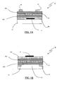
- FIG. 1 A possible architecture of an OLET to which the previous teachings for the realization of an OLET with distributed light emission apply, is shown in figure 1 .
- the light emitting transistor 10 comprises a substrate 11 that acts as a supporting layer, over which there is an electrode 12 that acts as control or gate electrode, and the layer of dielectric material Die, over which there is the first one of the two semiconductor layers SC1 of the ambipolar channel of the transistor.
- the semiconductor layer SC1 there is the light emitting layer R, over which on its turn the second semiconductor layer SC2 is deposited.
- the OLET structure 20 contemplates the deposition of the source and drain electrodes 13 and 13', that are deposited directly on the substrate 11. These electrodes are in contact with the semiconductor layer SC2, that is surmounted by the light emitting layer R, over which on its turn is deposited the semiconductor layer SC1, surmounted by the dielectric layer Die on which the gate electrode 12 is deposited.
- a definitely equivalent variant of the structure shown in figure 1A does not use an element 11 as supporting substrate, instead its function is performed by the gate electrode itself, that in this case has an amplitude greater than that depicted in figure 1 , or the indicated substrate as single element 11 is in reality composed by a plurality of elements.
- the materials that compose the electrodes 13 and 13' may be optimized in function of the type of charge (electrons, holes) that should be injected.
- oligoacenes oligothiophenes and oligofluorenes
- pyrimidine derivatives of oligothiophenes tetrathiophenes substituted in positions ⁇ and ⁇ with alkylic chains, the latter being preferred because of the small surface roughness and the great field effect mobility.
- diimide derivatives of perylenes and oligothiophenes there are diimide derivatives of perylenes and oligothiophenes, pyrimidine derivatives of oligothiophenes, oligothiophenes with thiazole core, coronene derivatives and derivatives of tetrathiophene substituted in positions ⁇ and ⁇ with perfluorated chains, the latter being preferred because of the great field effect mobility.
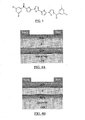
- suitable materials adapted to the realization of the invention are Alq 3 , cyclometalated platinum complexes of the type 1,3-di(2-pyridyl)-5-Methyl-benzene platinum(II) chloride, or Host-Guest systems with quinoline Aluminum lattice doped in various manners with, for example, 4-(dicyanomethylen)-2-methyl-6-(p-dimethylaminostyryl)-4H-pyrane, Platinum octaethyl-porphyryn, phenylisoquinoline of Iridium acetylacetonate, or Host-Guest systems with Aluminum quinoline lattice doped with a combination of these molecules.
- Example 1 The invention is better described hereinafter through a non limiting example of an embodiment (Example 1). Counter-examples are also provided in which the light emission is spatially confined (Example 2, Example 3 and Example 4) because both the above conditions 1 and 2 are not verified at the same time.
- An organic ambipolar light emitting field effect transistor with distributed light emission is realized from a substrate that comprises a first layer of glass on which there is a layer of ITO (Indium Tin Oxide), on which there is a layer of polymethylmethacrylate (PMMA) as dielectric Die.
- the first layer of semiconductor material SC1 is deposited over the layer of PMMA, in this case a layer of 15 nm made of dihexyl-tetrathiophene (DH4T) as layer for carrying holes.
- a 40 nm layer of light emitting material composed of a Host-Guest mixture of tris 8-hydroxyquinolato aluminum (Alq 3 ) containing 8% by weight of platinum octaethyl-porphyrin (PtOEP), and finally the last element of the three-layer stack, the semiconductor SC2 for carrying electrons, made of di-perflouro-hexyl-tetrathiophene (DHF4T), having a thickness of 20 nm.
- DHF4T di-perflouro-hexyl-tetrathiophene
- the stack of the three layers, DH4T, Alq 3 + PtOEP and DHF4T constitutes the ambipolar channel of the transistor.
- DH4T was subjected to two recrystallization processes, and the DHF4T was subjected to two sublimation processes at temperature with controlled gradient.
- the implemented processes have reduced impurities in the interval 0.02-0.001 % for both materials; Alq 3 is pure at 99.99%.
- the degree of purity of materials ensures that the effective field effect mobilities of both carries are sufficiently close to each other for having a wide illumination of the channel, using materials and related purification processes that allow the realization of devices on an industrial scale.
- the transistor in order to measure the effective field effect mobility, the transistor is operated in unipolar mode.
- condition 2 that is about the different constraints on the values of the energy levels, they are all verified, as it is possible to infer from the scheme depicted in Figure 8A .
- the transistor realized as in the example 1 is operated in an ambipolar functioning condition, by setting a potential difference between gate and source Vgs of -60V, and a potential difference between drain and source Vds of -100V and its light emission is collected through a Nikon Eclipse 2000-E microscope with 60x magnification and 0.7 numerical aperture.
- An organic ambipolar light emitting field effect transistor is realized exactly with the same materials, the same structure and the same thicknesses used in the Example 1. Nevertheless, in this example, the growth rate in the two layers of DH4T and DFH4T was controlled and set to 0.1 Angstrom/s, and the growth rate for the Alq 3 layer was set to 2 Angstrom/s. All the other characteristics of the device, including the insertion of PtOEP in Alq 3 performed through controlled co-deposition in the percentage of 8%, remain unchanged.
- the overall structure of the device is thus ITO/PMMA/DH4T (15 nm, 0.1 A/s)/Alq3:PtOEP 8% (40 nm, 2 A/s)/DHF4T (20 nm, 0.1 A/s)/Au (50 nm).
- V T N 30V
- V T P -57V
- condition on the effective mobility is a cardinal element in order to achieve a distributed light emission as comparative example 2 clearly shows.
- Such condition was not disclosed or described in the already referenced 2010 Nature Materials paper "Organic light-emitting transistors with an efficiency that outperforms the equivalent light-emitting diodes ", that shows OLET with narrow and well defined light spatial emission without no teaching or suggestion on how to alter or achieve a distributed light emission.
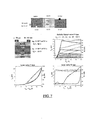
- an OLET architecture the scheme of which is depicted in figure 7 , in which a layer of semiconductor material DH4T (30 nm thickness) with P-type mobility is deposited on the PMMA dielectric.
- a layer of Alq 3 having a thickness of 30 nm, that acts as light emitting layer.
- the layer SC2 with N-type mobility in contact with the gold electrodes is composed of a layer having a thickness of 30 nm of an arylcarbonylic derivative of tetrathiophene (SLV-131), having the empirical formula C 30 H 14 O 2 S 4 F 4 and having the molecular structure depicted in Fig. 3 .
- the architecture of figure 7 shows that the condition 2) about energy levels is complied with, though the structure of this example is characterized by a ratio of two orders of magnitude between the effective field effect mobility values at the respective interfaces of SC1 and of SC2.
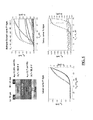
- the fact of not having satisfied even only the condition 1) caused a reduction of the amplitude of the light emitting area to about 10 ⁇ m, as demonstrated in Fig. 2B in which a 3D digital elaboration of the illuminated channel, in an ambipolar functioning condition, is depicted.
- An organic ambipolar light emitting field effect transistor is realized starting from a substrate that comprises a first layer of glass over which there is a layer of ITO (Indium Tin Oxide), over which there is a layer of polymethylmethacrylate (PMMA) that acts as dielectric Die.
- the first layer of semiconductor material SC1 is deposited on the layer of PMMA, in this case a 10 nm layer made of di-hexyl-tetrathiophene (DH4T) as layer for carrying holes.
- TCTA Tris(4-carbazoyl-9-ylphenyl)amine
- DHF4T di-perfluoro-hexyl-tetrathiophene
- the stack of the three layers DH4T, TCTA and DHF4T constitutes the ambipolar channel of the transistor.
- the process for growing the structure has been optimized by using techniques that are widespread in the field and well known to the skilled persons for not affecting the field effect mobility of the charge carriers, in particular the growing rate of the two layers of DH4T and DFH4T was controlled and set to 0.1 Angstrom/s, the growing rate of the layer of TCTA was set to 5 Angstrom/s.
- the condition 1) about the ratio between the values of the effective mobilities was satisfied.
- the energy levels of the levels HOMO and LUMO of the used materials are not complying with condition 2) and the emission of the light emitting ambipolar transistor is spatially confined. Indeed, as it may be inferred from figures 8C and 8D , the conditions about the energy differences between LUMO-R and LUMO-SCn, that is 0.9 eV, thus out of the requested range [from 0.2 eV to 0.8 eV], is not satisfied.
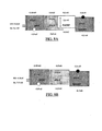
- FIGS 4A and 4B depict possible architectures of an OLET device in which the layer in contact with the dielectric is respectively of P-type (SCP) or of N-type (SCN).
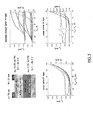
- Figure 5 shows an example of architecture of an OLET device with distributed illumination, experimentally tested, and the related graphs of the voltage-current and voltage-emission characteristics obtained with the described architectural features.
- the recombination layer in this case is composed of TCTA:DCM2. It is to be noticed that the effective mobilities differ between them by less than 20 times, i.e. the ratio of the maximum value, 0.28 cm 2 /Vs for the negative carriers, with the minimum value of 0.11 cm 2 /Vs for the positive carriers, is 2.54, well within the limit value of 20 as imposed by condition 1),. Also condition 2) is complied as shown in Fig. 8D .
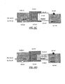
- Figure 6 is similar to figure 5 and shows another exemplary architecture of an OLET device with distributed illumination and the related graphs of the voltage-current and voltage-emission characteristics.
- the recombination layer is composed of TCTA-PtOEP.
- the effective mobile of the negative carriers is the lowest one, 0.051 cm 2 /Vs, while the effective mobility of the positive carriers is 0.7 cm 2 /Vs, resulting in a ratio of 13.7.
- condition 2) is complied as shown in Fig. 8C .
- Figure 7 shows an architecture of an OLET device not according to this invention with a P-type semiconductor layer (DH4T) in contact with the dielectric, a light emitting layer made of tris 8-hydroxyquinolato aluminum (Alq 3 ), a N-type semiconductor layer (SLV131) placed on the light emitting layer.
- a P-type semiconductor layer Diffraction-based light emitting layer
- Alq 3 tris 8-hydroxyquinolato aluminum
- SLV131 N-type semiconductor layer
- the OLET device of figure 7 has therefore a spatially confined illumination.
- Figures from 8A to 8D illustrate the LUMO and HOMO levels of materials usable for realizing the novel device, together with the Fermi level of the source and drain contacts.
- the condition 2) is satisfied thus they are suitable for realizing the novel OLET device with distributed illumination, provided that they are deposited in a way to make the effective field effect mobilities at the interfaces not differing from each other by more than 20 times.
Landscapes
- Physics & Mathematics (AREA)
- Optics & Photonics (AREA)
- Electroluminescent Light Sources (AREA)
- Thin Film Transistor (AREA)
Applications Claiming Priority (2)
| Application Number | Priority Date | Filing Date | Title |
|---|---|---|---|
| IT000284A ITMI20120284A1 (it) | 2012-02-27 | 2012-02-27 | Transistor ambipolare elettroluminescente organico ad effetto di campo ad emissione luminosa distribuita |
| PCT/IB2013/051400 WO2013128344A1 (en) | 2012-02-27 | 2013-02-21 | Organic light emitting ambipolar field effect transistor with distributed light emission |
Publications (2)
| Publication Number | Publication Date |
|---|---|
| EP2786437A1 EP2786437A1 (en) | 2014-10-08 |
| EP2786437B1 true EP2786437B1 (en) | 2015-03-25 |
Family
ID=45999947
Family Applications (1)
| Application Number | Title | Priority Date | Filing Date |
|---|---|---|---|
| EP13716411.7A Not-in-force EP2786437B1 (en) | 2012-02-27 | 2013-02-21 | Organic light emitting ambipolar field effect transistor with distributed light emission |
Country Status (8)
| Country | Link |
|---|---|
| US (1) | US9006726B2 (enExample) |
| EP (1) | EP2786437B1 (enExample) |
| JP (1) | JP6025874B2 (enExample) |
| KR (1) | KR101839649B1 (enExample) |
| CN (1) | CN104094436B (enExample) |
| IT (1) | ITMI20120284A1 (enExample) |
| TW (1) | TWI573305B (enExample) |
| WO (1) | WO2013128344A1 (enExample) |
Families Citing this family (14)
| Publication number | Priority date | Publication date | Assignee | Title |
|---|---|---|---|---|
| EP2911214B1 (en) | 2014-02-20 | 2018-08-08 | Amorosi, Antonio | Multilayer structure of an OLET transistor |
| EP2960280A1 (en) | 2014-06-26 | 2015-12-30 | E.T.C. S.r.l. | Photocrosslinkable compositions, patterned high k thin film dielectrics and related devices |
| EP2978038A1 (en) | 2014-07-24 | 2016-01-27 | E.T.C. S.r.l. | Organic electroluminescent transistor |
| CN111146352B (zh) * | 2014-07-24 | 2022-10-21 | 飞利斯有限公司 | 有机电致发光晶体管 |
| EP3021373A1 (en) * | 2014-11-14 | 2016-05-18 | E.T.C. S.r.l. | Display containing improved pixel architectures |
| WO2016100983A1 (en) | 2014-12-19 | 2016-06-23 | Polyera Corporation | Photocrosslinkable compositions, patterned high k thin film dielectrics and related devices |
| JP6546400B2 (ja) * | 2015-02-05 | 2019-07-17 | 株式会社ジャパンディスプレイ | 表示装置 |
| CN105355799A (zh) * | 2015-10-12 | 2016-02-24 | Tcl集团股份有限公司 | 一种量子点发光场效应晶体管及其制备方法 |
| CN106684153A (zh) * | 2015-11-05 | 2017-05-17 | 中国科学院宁波材料技术与工程研究所 | 自驱动发光薄膜晶体管,薄膜晶体管阵列及显示装置 |
| WO2019139175A1 (en) * | 2018-01-09 | 2019-07-18 | Kyushu University, National University Corporation | Organic light-emitting field-effect transistor |
| WO2020136420A1 (en) * | 2018-12-27 | 2020-07-02 | Bio-On S.P.A. | Piezoelectric device comprising a membrane comprising fibres of a polyhydroxyalkanoate |
| CN111081740A (zh) * | 2019-12-06 | 2020-04-28 | 深圳市华星光电半导体显示技术有限公司 | 一种显示面板 |
| CN115207238B (zh) * | 2022-07-01 | 2024-12-03 | 闽都创新实验室 | 一种具有光电双输出的发光突触晶体管及其制备方法 |
| TWI864513B (zh) * | 2022-11-30 | 2024-12-01 | 國立成功大學 | 發光裝置及發光裝置之製備方法 |
Family Cites Families (10)
| Publication number | Priority date | Publication date | Assignee | Title |
|---|---|---|---|---|
| CN1398146A (zh) * | 2002-08-13 | 2003-02-19 | 清华大学 | 一种有机电致发光器件 |
| US6970490B2 (en) * | 2002-05-10 | 2005-11-29 | The Trustees Of Princeton University | Organic light emitting devices based on the formation of an electron-hole plasma |
| EP1609195B9 (en) | 2003-03-28 | 2011-08-31 | Michele Muccini | Organic electroluminescence devices |
| US20060261329A1 (en) * | 2004-03-24 | 2006-11-23 | Michele Muccini | Organic electroluminescence devices |
| CN100508238C (zh) * | 2004-05-11 | 2009-07-01 | Lg化学株式会社 | 有机电子器件 |
| US7528176B2 (en) * | 2004-09-14 | 2009-05-05 | Northwestern University | Carbonyl-functionalized thiophene compounds and related device structures |
| EP2083456B1 (en) * | 2006-11-14 | 2013-01-02 | Idemitsu Kosan Co., Ltd. | Organic thin film transistor and organic thin film light-emitting transistor |
| CN102203974A (zh) | 2008-10-29 | 2011-09-28 | 皇家飞利浦电子股份有限公司 | 双栅极场效应晶体管和生产双栅极场效应晶体管的方法 |
| JP5666474B2 (ja) * | 2009-12-14 | 2015-02-12 | 出光興産株式会社 | 多環縮環化合物、及び、それを用いた有機薄膜トランジスタ |
| US8598448B2 (en) | 2010-03-20 | 2013-12-03 | Polyera Corporation | Pyrrolo[3,2-B]pyrrole semiconducting compounds and devices incorporating same |
-
2012
- 2012-02-27 IT IT000284A patent/ITMI20120284A1/it unknown
-
2013
- 2013-02-21 WO PCT/IB2013/051400 patent/WO2013128344A1/en not_active Ceased
- 2013-02-21 KR KR1020147020705A patent/KR101839649B1/ko not_active Expired - Fee Related
- 2013-02-21 US US14/373,225 patent/US9006726B2/en active Active
- 2013-02-21 EP EP13716411.7A patent/EP2786437B1/en not_active Not-in-force
- 2013-02-21 CN CN201380006607.4A patent/CN104094436B/zh not_active Expired - Fee Related
- 2013-02-21 JP JP2014558244A patent/JP6025874B2/ja not_active Expired - Fee Related
- 2013-02-22 TW TW102106218A patent/TWI573305B/zh not_active IP Right Cessation
Also Published As
| Publication number | Publication date |
|---|---|
| JP6025874B2 (ja) | 2016-11-16 |
| ITMI20120284A1 (it) | 2013-08-28 |
| CN104094436B (zh) | 2016-08-24 |
| KR101839649B1 (ko) | 2018-03-16 |
| JP2015513795A (ja) | 2015-05-14 |
| WO2013128344A1 (en) | 2013-09-06 |
| US20150001518A1 (en) | 2015-01-01 |
| CN104094436A (zh) | 2014-10-08 |
| TW201349606A (zh) | 2013-12-01 |
| US9006726B2 (en) | 2015-04-14 |
| TWI573305B (zh) | 2017-03-01 |
| KR20140126699A (ko) | 2014-10-31 |
| EP2786437A1 (en) | 2014-10-08 |
Similar Documents
| Publication | Publication Date | Title |
|---|---|---|
| EP2786437B1 (en) | Organic light emitting ambipolar field effect transistor with distributed light emission | |
| Chauhan et al. | Organic devices: fabrication, applications, and challenges | |
| Son et al. | Transparent and flexible ultraviolet photodetectors based on colloidal ZnO quantum dot/graphene nanocomposites formed on poly (ethylene terephthalate) substrates | |
| Maria Angela et al. | Organic light-emitting transistors: from understanding to molecular design and architecture | |
| Chen et al. | High-performance quantum-dot light-emitting transistors based on vertical organic thin-film transistors | |
| US9496315B2 (en) | Top-gate bottom-contact organic transistor | |
| EP2583329B1 (en) | Electroluminescent organic transistor | |
| Song et al. | Improved performance of organic light-emitting field-effect transistors by interfacial modification of hole-transport layer/emission layer: Incorporating organic heterojunctions | |
| WO2016014980A1 (en) | Organic electroluminescent transistor | |
| Ganesan et al. | En Route to Wide Area Emitting Organic Light‐Emitting Transistors for Intrinsic Drive‐Integrated Display Applications: A Comprehensive Review | |
| Yumusak et al. | Optical and electrical properties of electrochemically doped organic field effect transistors | |
| Zhao et al. | Improving the performance of red organic light-emitting transistors by utilizing a high-k organic/inorganic bilayer dielectric | |
| Cui et al. | Light emitting field-effect transistors with vertical heterojunctions based on pentacene and tris-(8-hydroxyquinolinato) aluminum | |
| Song et al. | Pixeled electroluminescence from multilayer heterostructure organic light-emitting transistors | |
| Aleshin | Organic optoelectronics based on polymer-inorganic nanoparticle composite materials | |
| Ng et al. | Near infrared emission in rubrene: fullerene heterojunction devices | |
| Kim et al. | Effects of doping and electrode contacts on performance of organic light-emitting transistors based on pentacene and tris (8-hydroxyquinoline) aluminum | |
| Generali et al. | Ambipolar field-effect transistor based on α, ω-dihexylquaterthiophene and α, ω-diperfluoroquaterthiophene vertical heterojunction | |
| Kim et al. | Organic light-emitting transistors based on pentacene and 4, 5-Di (9 H-carbazol-9-yl) phthalonitrile doped onto 1, 3-Bis (N-carbazolyl) benzene | |
| El Amrani et al. | Organic optocoupler consisting of an optimized blue organic light emitting diode and an organic photoconductor | |
| Feldmeier et al. | Multiple colour emission from an organic light-emitting transistor | |
| Li et al. | Performance Improvement of Gate-Tunable Organic Light-Emitting Diodes with Electron-Transport and Hole-Blocking Layers | |
| Generali et al. | Multilayer approach in light-emitting transistors | |
| 박재현 et al. | Steric Effect on Excimer Formation in Planar Pt (II) Complexes | |
| 서의현 et al. | Doping of Shallow HOMO Level Donor-Acceptor Polymers via Solution Mixing for Organic Thermoelectric Devices |
Legal Events
| Date | Code | Title | Description |
|---|---|---|---|
| PUAI | Public reference made under article 153(3) epc to a published international application that has entered the european phase |
Free format text: ORIGINAL CODE: 0009012 |
|
| GRAP | Despatch of communication of intention to grant a patent |
Free format text: ORIGINAL CODE: EPIDOSNIGR1 |
|
| 17P | Request for examination filed |
Effective date: 20140703 |
|
| AK | Designated contracting states |
Kind code of ref document: A1 Designated state(s): AL AT BE BG CH CY CZ DE DK EE ES FI FR GB GR HR HU IE IS IT LI LT LU LV MC MK MT NL NO PL PT RO RS SE SI SK SM TR |
|
| INTG | Intention to grant announced |
Effective date: 20141007 |
|
| GRAS | Grant fee paid |
Free format text: ORIGINAL CODE: EPIDOSNIGR3 |
|
| GRAA | (expected) grant |
Free format text: ORIGINAL CODE: 0009210 |
|
| AK | Designated contracting states |
Kind code of ref document: B1 Designated state(s): AL AT BE BG CH CY CZ DE DK EE ES FI FR GB GR HR HU IE IS IT LI LT LU LV MC MK MT NL NO PL PT RO RS SE SI SK SM TR |
|
| DAX | Request for extension of the european patent (deleted) | ||
| REG | Reference to a national code |
Ref country code: GB Ref legal event code: FG4D |
|
| REG | Reference to a national code |
Ref country code: CH Ref legal event code: EP |
|
| REG | Reference to a national code |
Ref country code: IE Ref legal event code: FG4D |
|
| REG | Reference to a national code |
Ref country code: DE Ref legal event code: R096 Ref document number: 602013001322 Country of ref document: DE Effective date: 20150507 |
|
| REG | Reference to a national code |
Ref country code: AT Ref legal event code: REF Ref document number: 718334 Country of ref document: AT Kind code of ref document: T Effective date: 20150515 |
|
| REG | Reference to a national code |
Ref country code: NL Ref legal event code: T3 |
|
| PG25 | Lapsed in a contracting state [announced via postgrant information from national office to epo] |
Ref country code: LT Free format text: LAPSE BECAUSE OF FAILURE TO SUBMIT A TRANSLATION OF THE DESCRIPTION OR TO PAY THE FEE WITHIN THE PRESCRIBED TIME-LIMIT Effective date: 20150325 Ref country code: SE Free format text: LAPSE BECAUSE OF FAILURE TO SUBMIT A TRANSLATION OF THE DESCRIPTION OR TO PAY THE FEE WITHIN THE PRESCRIBED TIME-LIMIT Effective date: 20150325 Ref country code: FI Free format text: LAPSE BECAUSE OF FAILURE TO SUBMIT A TRANSLATION OF THE DESCRIPTION OR TO PAY THE FEE WITHIN THE PRESCRIBED TIME-LIMIT Effective date: 20150325 Ref country code: HR Free format text: LAPSE BECAUSE OF FAILURE TO SUBMIT A TRANSLATION OF THE DESCRIPTION OR TO PAY THE FEE WITHIN THE PRESCRIBED TIME-LIMIT Effective date: 20150325 |
|
| REG | Reference to a national code |
Ref country code: AT Ref legal event code: MK05 Ref document number: 718334 Country of ref document: AT Kind code of ref document: T Effective date: 20150325 |
|
| REG | Reference to a national code |
Ref country code: LT Ref legal event code: MG4D |
|
| PG25 | Lapsed in a contracting state [announced via postgrant information from national office to epo] |
Ref country code: RS Free format text: LAPSE BECAUSE OF FAILURE TO SUBMIT A TRANSLATION OF THE DESCRIPTION OR TO PAY THE FEE WITHIN THE PRESCRIBED TIME-LIMIT Effective date: 20150325 Ref country code: LV Free format text: LAPSE BECAUSE OF FAILURE TO SUBMIT A TRANSLATION OF THE DESCRIPTION OR TO PAY THE FEE WITHIN THE PRESCRIBED TIME-LIMIT Effective date: 20150325 Ref country code: GR Free format text: LAPSE BECAUSE OF FAILURE TO SUBMIT A TRANSLATION OF THE DESCRIPTION OR TO PAY THE FEE WITHIN THE PRESCRIBED TIME-LIMIT Effective date: 20150626 |
|
| PG25 | Lapsed in a contracting state [announced via postgrant information from national office to epo] |
Ref country code: ES Free format text: LAPSE BECAUSE OF FAILURE TO SUBMIT A TRANSLATION OF THE DESCRIPTION OR TO PAY THE FEE WITHIN THE PRESCRIBED TIME-LIMIT Effective date: 20150325 Ref country code: SK Free format text: LAPSE BECAUSE OF FAILURE TO SUBMIT A TRANSLATION OF THE DESCRIPTION OR TO PAY THE FEE WITHIN THE PRESCRIBED TIME-LIMIT Effective date: 20150325 Ref country code: PT Free format text: LAPSE BECAUSE OF FAILURE TO SUBMIT A TRANSLATION OF THE DESCRIPTION OR TO PAY THE FEE WITHIN THE PRESCRIBED TIME-LIMIT Effective date: 20150727 Ref country code: EE Free format text: LAPSE BECAUSE OF FAILURE TO SUBMIT A TRANSLATION OF THE DESCRIPTION OR TO PAY THE FEE WITHIN THE PRESCRIBED TIME-LIMIT Effective date: 20150325 Ref country code: CZ Free format text: LAPSE BECAUSE OF FAILURE TO SUBMIT A TRANSLATION OF THE DESCRIPTION OR TO PAY THE FEE WITHIN THE PRESCRIBED TIME-LIMIT Effective date: 20150325 Ref country code: RO Free format text: LAPSE BECAUSE OF FAILURE TO SUBMIT A TRANSLATION OF THE DESCRIPTION OR TO PAY THE FEE WITHIN THE PRESCRIBED TIME-LIMIT Effective date: 20150325 |
|
| PG25 | Lapsed in a contracting state [announced via postgrant information from national office to epo] |
Ref country code: IS Free format text: LAPSE BECAUSE OF FAILURE TO SUBMIT A TRANSLATION OF THE DESCRIPTION OR TO PAY THE FEE WITHIN THE PRESCRIBED TIME-LIMIT Effective date: 20150725 Ref country code: PL Free format text: LAPSE BECAUSE OF FAILURE TO SUBMIT A TRANSLATION OF THE DESCRIPTION OR TO PAY THE FEE WITHIN THE PRESCRIBED TIME-LIMIT Effective date: 20150325 Ref country code: AT Free format text: LAPSE BECAUSE OF FAILURE TO SUBMIT A TRANSLATION OF THE DESCRIPTION OR TO PAY THE FEE WITHIN THE PRESCRIBED TIME-LIMIT Effective date: 20150325 |
|
| REG | Reference to a national code |
Ref country code: DE Ref legal event code: R097 Ref document number: 602013001322 Country of ref document: DE |
|
| PG25 | Lapsed in a contracting state [announced via postgrant information from national office to epo] |
Ref country code: DK Free format text: LAPSE BECAUSE OF FAILURE TO SUBMIT A TRANSLATION OF THE DESCRIPTION OR TO PAY THE FEE WITHIN THE PRESCRIBED TIME-LIMIT Effective date: 20150325 |
|
| PLBE | No opposition filed within time limit |
Free format text: ORIGINAL CODE: 0009261 |
|
| STAA | Information on the status of an ep patent application or granted ep patent |
Free format text: STATUS: NO OPPOSITION FILED WITHIN TIME LIMIT |
|
| 26N | No opposition filed |
Effective date: 20160105 |
|
| PG25 | Lapsed in a contracting state [announced via postgrant information from national office to epo] |
Ref country code: SI Free format text: LAPSE BECAUSE OF FAILURE TO SUBMIT A TRANSLATION OF THE DESCRIPTION OR TO PAY THE FEE WITHIN THE PRESCRIBED TIME-LIMIT Effective date: 20150325 |
|
| PG25 | Lapsed in a contracting state [announced via postgrant information from national office to epo] |
Ref country code: MC Free format text: LAPSE BECAUSE OF FAILURE TO SUBMIT A TRANSLATION OF THE DESCRIPTION OR TO PAY THE FEE WITHIN THE PRESCRIBED TIME-LIMIT Effective date: 20150325 Ref country code: LU Free format text: LAPSE BECAUSE OF FAILURE TO SUBMIT A TRANSLATION OF THE DESCRIPTION OR TO PAY THE FEE WITHIN THE PRESCRIBED TIME-LIMIT Effective date: 20160221 |
|
| REG | Reference to a national code |
Ref country code: CH Ref legal event code: PL |
|
| PG25 | Lapsed in a contracting state [announced via postgrant information from national office to epo] |
Ref country code: CH Free format text: LAPSE BECAUSE OF NON-PAYMENT OF DUE FEES Effective date: 20160229 Ref country code: LI Free format text: LAPSE BECAUSE OF NON-PAYMENT OF DUE FEES Effective date: 20160229 |
|
| REG | Reference to a national code |
Ref country code: FR Ref legal event code: ST Effective date: 20161028 |
|
| REG | Reference to a national code |
Ref country code: IE Ref legal event code: MM4A |
|
| PG25 | Lapsed in a contracting state [announced via postgrant information from national office to epo] |
Ref country code: FR Free format text: LAPSE BECAUSE OF NON-PAYMENT OF DUE FEES Effective date: 20160229 Ref country code: IE Free format text: LAPSE BECAUSE OF NON-PAYMENT OF DUE FEES Effective date: 20160221 |
|
| PG25 | Lapsed in a contracting state [announced via postgrant information from national office to epo] |
Ref country code: MT Free format text: LAPSE BECAUSE OF FAILURE TO SUBMIT A TRANSLATION OF THE DESCRIPTION OR TO PAY THE FEE WITHIN THE PRESCRIBED TIME-LIMIT Effective date: 20150325 |
|
| PG25 | Lapsed in a contracting state [announced via postgrant information from national office to epo] |
Ref country code: SM Free format text: LAPSE BECAUSE OF FAILURE TO SUBMIT A TRANSLATION OF THE DESCRIPTION OR TO PAY THE FEE WITHIN THE PRESCRIBED TIME-LIMIT Effective date: 20150325 Ref country code: HU Free format text: LAPSE BECAUSE OF FAILURE TO SUBMIT A TRANSLATION OF THE DESCRIPTION OR TO PAY THE FEE WITHIN THE PRESCRIBED TIME-LIMIT; INVALID AB INITIO Effective date: 20130221 |
|
| PG25 | Lapsed in a contracting state [announced via postgrant information from national office to epo] |
Ref country code: CY Free format text: LAPSE BECAUSE OF FAILURE TO SUBMIT A TRANSLATION OF THE DESCRIPTION OR TO PAY THE FEE WITHIN THE PRESCRIBED TIME-LIMIT Effective date: 20150325 Ref country code: MK Free format text: LAPSE BECAUSE OF FAILURE TO SUBMIT A TRANSLATION OF THE DESCRIPTION OR TO PAY THE FEE WITHIN THE PRESCRIBED TIME-LIMIT Effective date: 20150325 Ref country code: MT Free format text: LAPSE BECAUSE OF FAILURE TO SUBMIT A TRANSLATION OF THE DESCRIPTION OR TO PAY THE FEE WITHIN THE PRESCRIBED TIME-LIMIT Effective date: 20160229 Ref country code: TR Free format text: LAPSE BECAUSE OF FAILURE TO SUBMIT A TRANSLATION OF THE DESCRIPTION OR TO PAY THE FEE WITHIN THE PRESCRIBED TIME-LIMIT Effective date: 20150325 Ref country code: NO Free format text: LAPSE BECAUSE OF NON-PAYMENT OF DUE FEES Effective date: 20150625 |
|
| PG25 | Lapsed in a contracting state [announced via postgrant information from national office to epo] |
Ref country code: BG Free format text: LAPSE BECAUSE OF FAILURE TO SUBMIT A TRANSLATION OF THE DESCRIPTION OR TO PAY THE FEE WITHIN THE PRESCRIBED TIME-LIMIT Effective date: 20150325 |
|
| PGFP | Annual fee paid to national office [announced via postgrant information from national office to epo] |
Ref country code: NO Payment date: 20160228 Year of fee payment: 4 |
|
| PG25 | Lapsed in a contracting state [announced via postgrant information from national office to epo] |
Ref country code: AL Free format text: LAPSE BECAUSE OF FAILURE TO SUBMIT A TRANSLATION OF THE DESCRIPTION OR TO PAY THE FEE WITHIN THE PRESCRIBED TIME-LIMIT Effective date: 20150325 |
|
| REG | Reference to a national code |
Ref country code: DE Ref legal event code: R082 Ref document number: 602013001322 Country of ref document: DE Representative=s name: COHAUSZ & FLORACK PATENT- UND RECHTSANWAELTE P, DE Ref country code: DE Ref legal event code: R081 Ref document number: 602013001322 Country of ref document: DE Owner name: FLEXTERRA, INC., SKOKIE, US Free format text: FORMER OWNER: E.T.C. S.R.L., BOLOGNA, IT |
|
| REG | Reference to a national code |
Ref country code: GB Ref legal event code: 732E Free format text: REGISTERED BETWEEN 20190411 AND 20190417 |
|
| REG | Reference to a national code |
Ref country code: NL Ref legal event code: HC Owner name: E.T.C. S.R.L. IN LIQUIDAZIONE; IT Free format text: DETAILS ASSIGNMENT: CHANGE OF OWNER(S), CHANGE OF OWNER(S) NAME; FORMER OWNER NAME: E.T.C. S.R.L. Effective date: 20190411 Ref country code: NL Ref legal event code: PD Owner name: FLEXTERRA, INC.; US Free format text: DETAILS ASSIGNMENT: CHANGE OF OWNER(S), ASSIGNMENT; FORMER OWNER NAME: E.T.C. S.R.L. IN LIQUIDAZIONE Effective date: 20190411 |
|
| REG | Reference to a national code |
Ref country code: BE Ref legal event code: FP Effective date: 20150601 Ref country code: BE Ref legal event code: HC Owner name: E.T.C. S.R.L. UNDER LIQUIDATION; IT Free format text: DETAILS ASSIGNMENT: CHANGE OF OWNER(S), CHANGEMENT DE NOM DU PROPRIETAIRE; FORMER OWNER NAME: E.T.C. S.R.L. Effective date: 20190411 Ref country code: BE Ref legal event code: PD Owner name: FLEXTERRA, INC.; US Free format text: DETAILS ASSIGNMENT: CHANGE OF OWNER(S), CESSION; FORMER OWNER NAME: E.T.C. S.R.L. UNDER LIQUIDATION Effective date: 20190411 |
|
| PG25 | Lapsed in a contracting state [announced via postgrant information from national office to epo] |
Ref country code: NO Free format text: LAPSE BECAUSE OF FAILURE TO SUBMIT A TRANSLATION OF THE DESCRIPTION OR TO PAY THE FEE WITHIN THE PRESCRIBED TIME-LIMIT Effective date: 20150625 |
|
| REG | Reference to a national code |
Ref country code: DE Ref legal event code: R079 Ref document number: 602013001322 Country of ref document: DE Free format text: PREVIOUS MAIN CLASS: H01L0051520000 Ipc: H10K0050800000 |
|
| P01 | Opt-out of the competence of the unified patent court (upc) registered |
Effective date: 20230521 |
|
| PGFP | Annual fee paid to national office [announced via postgrant information from national office to epo] |
Ref country code: NL Payment date: 20240226 Year of fee payment: 12 |
|
| PGFP | Annual fee paid to national office [announced via postgrant information from national office to epo] |
Ref country code: DE Payment date: 20240228 Year of fee payment: 12 Ref country code: GB Payment date: 20240227 Year of fee payment: 12 |
|
| PGFP | Annual fee paid to national office [announced via postgrant information from national office to epo] |
Ref country code: IT Payment date: 20240222 Year of fee payment: 12 Ref country code: BE Payment date: 20240227 Year of fee payment: 12 |
|
| REG | Reference to a national code |
Ref country code: DE Ref legal event code: R119 Ref document number: 602013001322 Country of ref document: DE |
|
| REG | Reference to a national code |
Ref country code: NL Ref legal event code: MM Effective date: 20250301 |
|
| GBPC | Gb: european patent ceased through non-payment of renewal fee |
Effective date: 20250221 |
|
| PG25 | Lapsed in a contracting state [announced via postgrant information from national office to epo] |
Ref country code: NL Free format text: LAPSE BECAUSE OF NON-PAYMENT OF DUE FEES Effective date: 20250301 |
|
| REG | Reference to a national code |
Ref country code: BE Ref legal event code: MM Effective date: 20250228 |
|
| PG25 | Lapsed in a contracting state [announced via postgrant information from national office to epo] |
Ref country code: DE Free format text: LAPSE BECAUSE OF NON-PAYMENT OF DUE FEES Effective date: 20250902 |
|
| PG25 | Lapsed in a contracting state [announced via postgrant information from national office to epo] |
Ref country code: GB Free format text: LAPSE BECAUSE OF NON-PAYMENT OF DUE FEES Effective date: 20250221 |
|
| PG25 | Lapsed in a contracting state [announced via postgrant information from national office to epo] |
Ref country code: IT Free format text: LAPSE BECAUSE OF NON-PAYMENT OF DUE FEES Effective date: 20250221 |
|
| PG25 | Lapsed in a contracting state [announced via postgrant information from national office to epo] |
Ref country code: BE Free format text: LAPSE BECAUSE OF NON-PAYMENT OF DUE FEES Effective date: 20250228 |