EP2780918B1 - Induktionsbauteil - Google Patents
Induktionsbauteil Download PDFInfo
- Publication number
- EP2780918B1 EP2780918B1 EP12772290.8A EP12772290A EP2780918B1 EP 2780918 B1 EP2780918 B1 EP 2780918B1 EP 12772290 A EP12772290 A EP 12772290A EP 2780918 B1 EP2780918 B1 EP 2780918B1
- Authority
- EP
- European Patent Office
- Prior art keywords
- coils
- coil
- induction component
- winding
- component according
- Prior art date
- Legal status (The legal status is an assumption and is not a legal conclusion. Google has not performed a legal analysis and makes no representation as to the accuracy of the status listed.)
- Active
Links
Images
Classifications
-
- H—ELECTRICITY
- H01—ELECTRIC ELEMENTS
- H01F—MAGNETS; INDUCTANCES; TRANSFORMERS; SELECTION OF MATERIALS FOR THEIR MAGNETIC PROPERTIES
- H01F19/00—Fixed transformers or mutual inductances of the signal type
-
- H—ELECTRICITY
- H01—ELECTRIC ELEMENTS
- H01F—MAGNETS; INDUCTANCES; TRANSFORMERS; SELECTION OF MATERIALS FOR THEIR MAGNETIC PROPERTIES
- H01F27/00—Details of transformers or inductances, in general
- H01F27/28—Coils; Windings; Conductive connections
- H01F27/29—Terminals; Tapping arrangements for signal inductances
-
- H—ELECTRICITY
- H01—ELECTRIC ELEMENTS
- H01F—MAGNETS; INDUCTANCES; TRANSFORMERS; SELECTION OF MATERIALS FOR THEIR MAGNETIC PROPERTIES
- H01F27/00—Details of transformers or inductances, in general
- H01F27/28—Coils; Windings; Conductive connections
- H01F27/2895—Windings disposed upon ring cores
Definitions
- the invention relates to an induction component.
- induction components With the constantly increasing switching frequency of electrical power circuits and controllers, new induction components are always required. These should primarily have a smaller inductance, for example in the switching frequency range between 10 MHz and 30 MHz an inductance between 100 nH and 300 nH for transformers and between 20 nH and 200 nH for inductors. In addition, these induction components should also have a smaller size.
- An induction component is already known that can be used both as an inductor and as a micro-transformer ( EP 1178504 A1 ).
- microtransformer in which individual turns of a conductor are arranged around an inner magnetic layer ( US 5976715 A ).
- a microtransformer which has a primary winding and a plurality of secondary windings on a magnetic core.
- the several secondary windings have their own connections ( US 2005/0017054 A1 ).
- the invention is based on the object of creating an induction component which offers a large number of different possible uses while requiring little space.
- the invention proposes an induction component with the features mentioned in claim 1. Further training is the subject of subclaims.
- the induction component By providing two coil devices, which are arranged on a common magnetic core, it is possible to use the induction component as a transformer. It is possible to select whether on the primary side as well as on the secondary side whether one or both coils of each coil device are used. This enables a transmission of 1: 1, 1: 2, 2: 1, 2: 2. If each coil device is made up of more than two coils, the number of possibilities is correspondingly greater.
- the induction component can also be used to represent an inductance with four different values, depending on how many of the existing coils are connected in series.
- Another advantage of the induction component proposed by the invention is that larger switching frequency ranges can be achieved with only one component can cover or that a component can be used for a wider range. If, for example, 3 coils are required for a switching frequency of 10 MHz, but only one coil is required for 20 MHz, this can be achieved with a single component. In this way, the selection of components is made easier for the user, procurement costs are reduced and the range of inductance values to be maintained becomes smaller.
- the profile size of such an induction component should, for example, be in a range from 0.5 to 0.3 mm or less.
- the sizes 1008, 0805, 0603, 0402, or 0201 can be mentioned as an example of the size of such components.
- the adjacent winding ends of two adjacent coils are connected to a common solder pad. This simplifies the interconnection of the individual coils and also the production, since the component in the example mentioned has only six soldering pads with two coil devices of two coils each.
- the ring has a rectangular shape and each of the two coil devices is formed on one leg of the rectangle.
- the invention proposes to produce the coils and their turns in a thin-film process.
- the individual conductor tracks of the turns are produced by a combination of sputtering and electroplating.
- the coils are produced by electroplating copper.
- the magnetic core is produced by depositing soft magnetic material, for example Ni, NiFe, CoFe, CoZrTi.
- the desired inductance to be produced can be set by the number of turns and the selection of the material of the magnetic core.
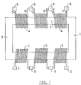
- the Figure 1 shows the top view of the induction component.
- it contains a magnetic core 1.
- This has the shape of a rectangular ring, with two legs 2 running in the longitudinal direction and two cross legs 3 connecting them
- a plurality of coils 4 are arranged around each longitudinal leg 2, all coils 4, 5 of a longitudinal leg 2 forming a coil device 6.
- the expression that the coils 4, 5 are wound can only be understood in terms of their function, since the coils are produced using the thin-film process, that is to say are not wound. This method of manufacturing coils is known per se.
- Each coil 4 has a winding start 7 and a winding end 8. All coils 4 are wound in the same direction, that is, they have the same winding sense. All coils 4 have the same number of turns. The coils 4 are arranged one behind the other in the longitudinal direction of the leg 2 and have a certain distance between them. The beginning of the winding 7 of the leftmost coil 4 is led out and connected to a solder pad 9. The winding end 8 of this coil is also led out and connected to a solder pad 9. The beginning of the winding 7 of the second coil is also connected to the same soldering pad 9. Its winding end 8 is in turn connected to a solder pad 9, to which the winding start 7 of the third coil is also connected.
- the induction component of the Figure 1 has a total of 8 connections.
- the induction component can be used as a transformer due to the division into 2 coil devices that are not electrically connected to one another.
- the following transmission ratios are possible: 1: 1, 1: 2, 1: 3; 2: 1, 2: 2, 2: 3; 3: 1, 3: 2, 3: 3.
- the induction component as an inductor
- using a series connection multiple coils can use both 4 and 5. It is therefore possible to implement an inductance with the inductance value of a coil up to the inductance value of 6 coils.
Landscapes
- Engineering & Computer Science (AREA)
- Power Engineering (AREA)
- Coils Or Transformers For Communication (AREA)
- Coils Of Transformers For General Uses (AREA)
Description
- Die Erfindung betrifft ein Induktionsbauteil.
- Mit ständig steigender Schaltfrequenz elektrischer Leistungsschaltungen und Controllern werden auch immer neue Induktionsbauteile benötigt. Diese sollen in erster Linie eine kleinere Induktivität aufweisen, beispielsweise im Schaltfrequenzbereich zwischen 10 MHz und 30 MHz eine Induktivität zwischen 100 nH und 300 nH für Transformatoren und zwischen 20 nH und 200 nH für Induktivitäten. Darüber hinaus sollen diese Induktionsbauteile auch eine kleinere Größe aufweisen.
- Es ist bereits ein Induktionsbauteil bekannt, dass sowohl als Induktivität als auch als Mikro- Transformator verwendet werden kann (
EP 1178504 A1 ). - Weiterhin ist ein Mikrotransformator bekannt, bei dem einzelnen Windungen eines Leiters um eine magnetische Innenlage herum angeordnet werden (
US 5976715 A ). - Es ist bereits ein Mikrotransformator bekannt, der auf einem Magnetkern eine Primärwicklung und mehrere Sekundärwicklungen aufweist. Die mehreren Sekundärwicklungen haben eigene herausgeführte Anschlüsse (
US 2005/0017054 A1 ). - Weiterhin bekannt ist ein Leistungsübertrager mit einer festen Primärwicklung und einer Sekundärwicklung, die eine Reihe von möglichen Zusammenschaltungen einzelner Wicklungen vorverdrahtet anbietet. Die einzelnen Wicklungen der Sekundärwicklung sind nicht direkt anschließbar (
WO 92/04723 - Bei einem nochmals weiteren bekannten Induktionsbauteil sind auf einem ringförmigen Kern drei Wicklungen vorhanden, deren Wicklungsenden zu einem Anschlussbauteil geführt werden, von dem aus die Wicklungen angesprochen werden können (
WO 2008/059392 A1 ). - Der Erfindung liegt die Aufgabe zu Grunde, ein Induktionsbauteil zu schaffen, das bei geringem Platzbedarf eine Vielzahl von verschiedenen Anwendungsmöglichkeiten bietet.
- Zur Lösung dieser Aufgabe schlägt die Erfindung ein Induktionsbauteil mit den im Anspruch 1 genannten Merkmalen vor. Weiterbildungen sind Gegenstand von Unteransprüchen.
- Durch das Vorsehen zweier Spuleneinrichtungen, die auf einem gemeinsamen Magnetkern angeordnet sind, ist es möglich, das Induktionsbauteil als Übertrager zu verwenden. Dabei ist es möglich, sowohl auf der Primärseite als auch auf der Sekundärseite auszuwählen, ob man eine oder beide Spulen jeder Spuleneinrichtung verwendet. Dadurch ist eine Übertragung von 1:1, 1:2, 2:1, 2:2 möglich. Wenn man jede Spuleneinrichtung aus mehr als zwei Spulen bestehen lässt, ist die Zahl der Möglichkeiten entsprechend größer.
- Bei dem einfachsten Beispiel mit zwei Spuleneinrichtungen, die jeweils aus zwei benachbarten Spulen bestehen, kann man das Induktionsbauteil auch zum Darstellen einer Induktivität mit vier verschiedenen Werten verwenden, je nachdem, wie viele der vorhandenen Spulen man hintereinander schaltet.
- Man hat also ein Induktionsbauteil geschaffen, das in dem gerade abgehandelten Beispiel acht verschiedene Anwendungsmöglichkeiten bietet.
- Ein weiterer Vorteil des von der Erfindung vorgeschlagenen Induktionsbauteils liegt darin, dass man mit nur einem Bauteil größere Schaltfrequenzbereiche abdecken kann bzw. dass ein Bauteil für eine größere Bandbreite eingesetzt werden kann. Wenn beispielsweise für eine Schaltfrequenz von 10 MHz 3 Spulen benötigt werden, für 20 MHz aber nur noch eine Spule benötigt wird, so kann dies mit einem einzigen Bauteil erreicht werden. Auf diese Weise wird die Bauteileauswahl für den Anwender erleichtert, Beschaffungskosten reduziert und das Spektrum von vorzuhaltenden Induktivitätswerten wird kleiner.
- Die Profilgröße eines solchen Induktionsbauteils soll beispielsweise in einem Bereich von 0.5 bis 0.3 mm oder darunter liegen können.
- Als Beispiel für die Größe solcher Bauteile können die Größen 1008, 0805, 0603, 0402, oder 0201 genannt werden.
- In Weiterbildung der Erfindung kann vorgesehen sein, dass die benachbarten Wicklungsenden jeweils zweier benachbarter Spulen mit einem gemeinsamen Lötpad verbunden sind. Damit vereinfacht sich die Zusammenschaltung der einzelnen Spulen und auch die Herstellung, da das Bauteil in dem erwähnten Beispiel mit zwei Spuleneinrichtungen von jeweils zwei Spulen nur sechs Lötpads aufweist.
- Insbesondere kann in Weiterbildung der Erfindung vorgesehen sein, dass der Ring Rechteckform aufweist und jede der beiden Spuleneinrichtungen an jeweils einem Schenkel des Rechtecks ausgebildet ist.
- In Weiterbildung der Erfindung kann vorgesehen sein, dass alle Spulen einer Spuleneinrichtung den gleichen Windungssinn aufweisen. Dabei ist es auch möglich, dass der Windungssinn in beiden Spuleneinrichtungen identisch ist.
- Obwohl es denkbar ist, dass die Zahl der Windungen bei jeder Spule und bei jeder Spuleneinrichtung unterschiedlich ist, kann erfindungsgemäß in Weiterbildung vorgesehen sein, dass alle Spulen einer Spuleneinrichtung die gleiche Windungszahl aufweisen, wobei insbesondere dies auch für die Spuleneinrichtungen untereinander gelten kann.
- Was für die Windungszahl und den Windungssinn gesagt wurde, kann in Weiterbildung der Erfindung auch für den Querschnitt der die Spulen bildenden elektrischen Leiter gelten.
- Die Erfindung schlägt vor, die Spulen und ihre Windungen in einem Dünnschichtverfahren herzustellen. Die einzelnen Leiterbahnen der Windungen werden durch eine Kombination von Sputtern und Elektroplatieren hergestellt. Insbesondere wird vorgesehen, dass die Spulen durch Elektroplatieren von Kupfer hergestellt werden.
- Der Magnetkern wird durch Ablagern weichen magnetischen Materials hergestellt, beispielsweise Ni, NiFe, CoFe, CoZrTi.
- Die gewünschte herzustellende Induktivität kann durch die Zahl der Windungen und die Auswahl des Materials des magnetischen Kerns eingestellt werden.
- Weitere Merkmale, Einzelheiten und Vorzüge der Erfindung ergeben sich aus den Ansprüchen und der Zusammenfassung, deren beider Wortlaut durch Bezugnahme zum Inhalt der Beschreibung gemacht wird, der folgenden Beschreibung bevorzugter Ausführungsformen der Erfindung sowie anhand der Zeichnung. Hierbei zeigen:
- Figur 1
- schematisch die Darstellung eines möglichen Induktionsbauteils nach der Erfindung.
- Die
Figur 1 zeigt die Draufsicht auf das Induktionsbauteil. Es enthält in der dargestellten Ausführungsform einen Magnetkern 1. Dieser weist die Form eines rechteckigen Rings auf, mit zwei in Längsrichtung verlaufenden Schenkeln 2 und zwei diese verbindenden Querschenkeln 3. Um jeden Längsschenkel 2 sind mehrere Spulen 4 herum angeordnet, wobei alle Spulen 4, 5 eines Längsschenkels 2 eine Spuleneinrichtung 6 bilden. Der Ausdruck, dass die Spulen 4, 5 gewickelt sind, ist nur in der Funktion zu verstehen, da die Spulen im Dünnschichtverfahren hergestellt, also nicht gewickelt werden. Dieses Verfahren zum Herstellen von Spulen ist an sich bekannt. - Jede Spule 4 hat einen Wicklungsanfang 7 und ein Wicklungsende 8. Alle Spulen 4 sind in der gleichen Richtung gewickelt, haben also den gleichen Windungssinn. Alle Spulen 4 haben die gleiche Anzahl von Windungen. Die Spulen 4 sind in Längsrichtung des Schenkels 2 hintereinander angeordnet und haben einen gewissen Abstand zwischen einander. Der Wicklungsanfang 7 der am weitesten links dargestellten Spule 4 ist herausgeführt und mit einem Lötpad 9 verbunden. Das Wicklungsende 8 dieser Spule ist ebenfalls herausgeführt und mit einem Lötpad 9 verbunden. Mit demselben Lötpad 9 ist auch der Wicklungsanfang 7 der zweiten Spule verbunden. Deren Wicklungsende 8 ist wiederum mit einem Lötpad 9 verbunden, mit dem auch der Wicklungsanfang 7 der dritten Spule verbunden ist.
- Alles, was für die Spulen 4 der ersten Spuleneinrichtung 6 gesagt wurde, gilt auch für die zweite in
Figur 1 unten dargestellte Spuleneinrichtung. Insbesondere können auch die Windungszahlen und der Windungssinn der Spulen untereinander gleich sein. - Das Induktionsbauteil der
Figur 1 hat insgesamt 8 Anschlüsse. Durch die Aufteilung in 2 Spuleneinrichtungen, die elektrisch nicht miteinander verbunden sind, kann das Induktionsbauteil als Transformator verwendet werden. Es sind folgende Übertragungsverhältnisse möglich: 1:1, 1:2, 1:3; 2:1, 2:2, 2:3; 3:1, 3:2, 3:3. - Es ist aber auch möglich, das Induktionsbauteil als Induktivität zu verwenden, wobei man eine Hintereinanderschaltung mehrerer Spulen sowohl 4 als auch 5 verwenden kann. Es lässt sich also eine Induktivität mit dem Induktivitätswert einer Spule bis zu dem Induktivitätswert von 6 Spulen verwirklichen.
Claims (7)
- Induktionsbauteil, mit1.1 einem Magnetkern (1) in Form eines geschlossenen Rings,1.2 mindestens zwei Spuleneinrichtungen (6) auf dem Kern (1), die elektrisch nicht miteinander verbunden sind, von denen1.3 jede Spuleneinrichtung (6) mindestens zwei benachbarte Spulen (4, 5) aufweist, wobei1.4. jede Spule (4, 5) einen Wicklungsanfang (7) und ein Wicklungsende (8) hat, und1.5 der Wicklungsanfang (7) und das Wicklungsende (8) jeder Spule (4, 5) nach außen geführt und mit Lötpads (9) verbunden sind, wobei1.6 die benachbarten Wicklungsanfänge (7) und Wicklungsenden (8) jeweils zweier benachbarter Spulen (4; 5) mit einem gemeinsamen Lötpad (9) verbunden sind.
- Induktionsbauteil nach Anspruch 1, bei dem der Ring Rechteckform aufweist und jede der beiden Spuleneinrichtungen (6) an jeweils einem Schenkel (2) ausgebildet ist.
- Induktionsbauteil nach einem der vorhergehenden Ansprüche, bei dem alle Spulen (4, 5) mindestens einer Spuleneinrichtung (6), vorzugsweise aller Spuleneinrichtungen (6), den gleichen Windungssinn aufweisen.
- Induktionsbauteil nach einem der vorhergehenden Ansprüche, bei dem alle Spulen (4, 5) mindestens einer Spuleneinrichtung (6), vorzugsweise aller Spuleneinrichtungen (6), die gleiche Windungszahl aufweisen.
- Induktionsbauteil nach einem der vorhergehenden Ansprüche, bei dem alle Spulen (4, 5) mindestens einer Spuleneinrichtung (6), vorzugsweise aller Spuleneinrichtungen (6), den gleichen Leitungsquerschnitt aufweisen.
- Induktionsbauteil nach einem der vorhergehenden Ansprüche, bei dem die Windungen der Spulen (4, 5) in Dünnschichttechnik hergestellte Windungen sind.
- Induktionsbauteil nach einem der vorhergehenden Ansprüche, bei dem der Magnetkern (1) ein in Dünnschichttechnik hergestellter Magnetkern ist.
Applications Claiming Priority (2)
| Application Number | Priority Date | Filing Date | Title |
|---|---|---|---|
| DE102011086403A DE102011086403A1 (de) | 2011-11-15 | 2011-11-15 | Induktionsbauteil |
| PCT/EP2012/069615 WO2013072135A1 (de) | 2011-11-15 | 2012-10-04 | Induktionsbauteil |
Publications (2)
| Publication Number | Publication Date |
|---|---|
| EP2780918A1 EP2780918A1 (de) | 2014-09-24 |
| EP2780918B1 true EP2780918B1 (de) | 2019-12-18 |
Family
ID=47018183
Family Applications (1)
| Application Number | Title | Priority Date | Filing Date |
|---|---|---|---|
| EP12772290.8A Active EP2780918B1 (de) | 2011-11-15 | 2012-10-04 | Induktionsbauteil |
Country Status (4)
| Country | Link |
|---|---|
| US (1) | US10510475B2 (de) |
| EP (1) | EP2780918B1 (de) |
| DE (1) | DE102011086403A1 (de) |
| WO (1) | WO2013072135A1 (de) |
Families Citing this family (2)
| Publication number | Priority date | Publication date | Assignee | Title |
|---|---|---|---|---|
| DE102014218043A1 (de) | 2014-09-10 | 2016-03-10 | Würth Elektronik eiSos Gmbh & Co. KG | Magnetkern, induktives Bauteil und Verfahren zum Herstellen eines Magnetkerns |
| JP6819564B2 (ja) * | 2017-12-19 | 2021-01-27 | 三菱電機株式会社 | 半導体装置およびその製造方法 |
Family Cites Families (26)
| Publication number | Priority date | Publication date | Assignee | Title |
|---|---|---|---|---|
| US1567672A (en) * | 1921-01-15 | 1925-12-29 | Underwood Typewriter Co | Electric motor |
| DE732281C (de) * | 1936-11-18 | 1943-02-26 | Aeg | Trockenmesswandler oder -drosselspule |
| US2491567A (en) * | 1947-02-24 | 1949-12-20 | Kendrick William | Leakage reactance transformer |
| DE942823C (de) * | 1954-04-16 | 1956-05-09 | Koch & Sterzel Ag | Hochspannungsseitig mit Anzapfungen versehener Hochspannungstransformator |
| US4825056A (en) * | 1985-11-21 | 1989-04-25 | Kabushiki Kaisha Toshiba | Thin-film electromagnetic transducer |
| US4777465A (en) * | 1986-04-28 | 1988-10-11 | Burr-Brown Corporation | Square toroid transformer for hybrid integrated circuit |
| JPH03110913A (ja) * | 1989-09-25 | 1991-05-10 | Mitsubishi Electric Corp | ラインフィルター |
| GB9019571D0 (en) | 1990-09-07 | 1990-10-24 | Electrotech Instr Ltd | Power transformers and coupled inductors with optimally interleaved windings |
| US5379207A (en) * | 1992-12-16 | 1995-01-03 | General Electric Co. | Controlled leakage field multi-interphase transformer employing C-shaped laminated magnetic core |
| JP2826930B2 (ja) | 1992-12-25 | 1998-11-18 | 太陽誘電株式会社 | リード端子を有する電子部品の製造方法 |
| US5780175A (en) | 1996-02-02 | 1998-07-14 | Lucent Technologies Inc. | Articles comprising magnetically soft thin films and methods for making such articles |
| JP3236521B2 (ja) | 1996-10-28 | 2001-12-10 | 株式会社トーキン | 薄形トランス及びその製造方法 |
| US6111451A (en) * | 1997-05-19 | 2000-08-29 | Micron Technology, Inc. | Efficient VCCP supply with regulation for voltage control |
| US5939955A (en) * | 1997-06-10 | 1999-08-17 | Bel Fuse, Inc. | Assembly of inductors wound on bobbin of encapsulated electrical components |
| JP3624840B2 (ja) * | 2000-05-16 | 2005-03-02 | Fdk株式会社 | インダクタ |
| FR2812756B1 (fr) | 2000-08-04 | 2002-10-04 | Memscap | Microcomposant du type micro-inductance ou micro- transformateur |
| US6927663B2 (en) * | 2003-07-23 | 2005-08-09 | Cardiac Pacemakers, Inc. | Flyback transformer wire attach method to printed circuit board |
| US6998952B2 (en) * | 2003-12-05 | 2006-02-14 | Freescale Semiconductor, Inc. | Inductive device including bond wires |
| US7791440B2 (en) * | 2004-06-09 | 2010-09-07 | Agency For Science, Technology And Research | Microfabricated system for magnetic field generation and focusing |
| US7161458B2 (en) * | 2005-02-22 | 2007-01-09 | Delta Electronics, Inc. | Electromagnetic device having independent inductive components |
| JP4266951B2 (ja) * | 2005-03-31 | 2009-05-27 | Tdk株式会社 | 磁気素子および電源装置 |
| US8350657B2 (en) * | 2005-06-30 | 2013-01-08 | Derochemont L Pierre | Power management module and method of manufacture |
| FR2897485B1 (fr) * | 2006-02-10 | 2008-06-06 | Artus Soc Par Actions Simplifi | Convertisseur ac/dc a autotransformateur |
| US7952460B2 (en) * | 2006-11-14 | 2011-05-31 | Nxp B.V. | Manufacturing of an electronic circuit having an inductance |
| JP4674590B2 (ja) * | 2007-02-15 | 2011-04-20 | ソニー株式会社 | バラントランス及びバラントランスの実装構造、並びに、この実装構造を内蔵した電子機器 |
| JP2009146955A (ja) * | 2007-12-11 | 2009-07-02 | Hitachi Computer Peripherals Co Ltd | 複合リアクトルおよび電源装置 |
-
2011
- 2011-11-15 DE DE102011086403A patent/DE102011086403A1/de not_active Withdrawn
-
2012
- 2012-10-04 US US14/350,286 patent/US10510475B2/en active Active
- 2012-10-04 EP EP12772290.8A patent/EP2780918B1/de active Active
- 2012-10-04 WO PCT/EP2012/069615 patent/WO2013072135A1/de not_active Ceased
Non-Patent Citations (1)
| Title |
|---|
| None * |
Also Published As
| Publication number | Publication date |
|---|---|
| US10510475B2 (en) | 2019-12-17 |
| HK1197313A1 (zh) | 2015-01-09 |
| US20140285300A1 (en) | 2014-09-25 |
| EP2780918A1 (de) | 2014-09-24 |
| WO2013072135A1 (de) | 2013-05-23 |
| DE102011086403A1 (de) | 2013-05-16 |
| CN104106117A (zh) | 2014-10-15 |
Similar Documents
| Publication | Publication Date | Title |
|---|---|---|
| DE3418379A1 (de) | Schichtfoermig aufgebaute induktionsspule | |
| DE102016210746B4 (de) | Induktives Bauelement, stromkompensierte Drossel und Verfahren zum Herstellen eines induktiven Bauelements | |
| DE102018115654A1 (de) | Aktiv gekühlte Spule | |
| DE102015107203A1 (de) | Magnetvorrichtungen und Herstellungsverfahren die Flex-Schaltkreise verwenden | |
| WO2019120882A1 (de) | Transformatorkern und transformator | |
| DE10125080A1 (de) | Induktives elektrisches Bauelement, insbesondere Ferritantenne, sowie Verfahren zur Herstellung und zum Abgleich desselben | |
| DE4115394A1 (de) | Duennschicht-magnetkopf | |
| DE102010014281A9 (de) | Induktive elektronische Baugruppe und Verwendung einer solchen | |
| DE202019102273U1 (de) | Induktives Bauelement | |
| EP2867906B1 (de) | Induktives bauteil | |
| EP2863403B1 (de) | Transformator | |
| DE102016219491A1 (de) | Spuleneinheit zum induktiven Laden eines Fahrzeuges | |
| EP2780918A1 (de) | Induktionsbauteil | |
| DE102014117551A1 (de) | Mehrfachdrossel und Leistungswandler mit einer Mehrfachdrossel | |
| EP3192090B1 (de) | Magnetkern, induktives bauteil und verfahren zum herstellen eines magnetkerns | |
| DE4214789C1 (en) | Transformer for high frequency applications - has annular ferrite core wound with pair of wire coils with core and components mounted on PCB | |
| DE2328024C3 (de) | Mittelfrequenz-Leistungstransformator mit einer zur starren Verbindung mit einem kühlmitteldurchflossenen Induktor geeigneten Sekundärwicklung | |
| DE3108161A1 (de) | Wicklung fuer eine statische induktionsvorrichtung | |
| DE102006051234A1 (de) | Transversalflussmaschine mit erhöhtem Wickelraum | |
| DE102012101988B4 (de) | Anordnung einer Luft-Drosselspule und eines Umschalters sowie Verfahren zur Herstellung einer solchen Anordnung | |
| DE102010049668A1 (de) | Transformator | |
| DE102021003119A1 (de) | Matrixtransformator | |
| EP3921859A1 (de) | Sekundärspulentopologie | |
| DE1488031B2 (de) | Wicklung für eine mehrpolige elektrische Maschine | |
| EP3707736B1 (de) | Transformator zur verwendung in einem schienenfahrzeug |
Legal Events
| Date | Code | Title | Description |
|---|---|---|---|
| PUAI | Public reference made under article 153(3) epc to a published international application that has entered the european phase |
Free format text: ORIGINAL CODE: 0009012 |
|
| 17P | Request for examination filed |
Effective date: 20140319 |
|
| AK | Designated contracting states |
Kind code of ref document: A1 Designated state(s): AL AT BE BG CH CY CZ DE DK EE ES FI FR GB GR HR HU IE IS IT LI LT LU LV MC MK MT NL NO PL PT RO RS SE SI SK SM TR |
|
| RIN1 | Information on inventor provided before grant (corrected) |
Inventor name: DINULOVIC, DRAGAN Inventor name: GERFER, ALEXANDER |
|
| REG | Reference to a national code |
Ref country code: HK Ref legal event code: DE Ref document number: 1197313 Country of ref document: HK |
|
| DAX | Request for extension of the european patent (deleted) | ||
| STAA | Information on the status of an ep patent application or granted ep patent |
Free format text: STATUS: EXAMINATION IS IN PROGRESS |
|
| 17Q | First examination report despatched |
Effective date: 20170905 |
|
| GRAP | Despatch of communication of intention to grant a patent |
Free format text: ORIGINAL CODE: EPIDOSNIGR1 |
|
| STAA | Information on the status of an ep patent application or granted ep patent |
Free format text: STATUS: GRANT OF PATENT IS INTENDED |
|
| INTG | Intention to grant announced |
Effective date: 20190528 |
|
| GRAJ | Information related to disapproval of communication of intention to grant by the applicant or resumption of examination proceedings by the epo deleted |
Free format text: ORIGINAL CODE: EPIDOSDIGR1 |
|
| STAA | Information on the status of an ep patent application or granted ep patent |
Free format text: STATUS: EXAMINATION IS IN PROGRESS |
|
| GRAP | Despatch of communication of intention to grant a patent |
Free format text: ORIGINAL CODE: EPIDOSNIGR1 |
|
| STAA | Information on the status of an ep patent application or granted ep patent |
Free format text: STATUS: GRANT OF PATENT IS INTENDED |
|
| INTC | Intention to grant announced (deleted) | ||
| INTG | Intention to grant announced |
Effective date: 20190718 |
|
| GRAS | Grant fee paid |
Free format text: ORIGINAL CODE: EPIDOSNIGR3 |
|
| GRAA | (expected) grant |
Free format text: ORIGINAL CODE: 0009210 |
|
| STAA | Information on the status of an ep patent application or granted ep patent |
Free format text: STATUS: THE PATENT HAS BEEN GRANTED |
|
| AK | Designated contracting states |
Kind code of ref document: B1 Designated state(s): AL AT BE BG CH CY CZ DE DK EE ES FI FR GB GR HR HU IE IS IT LI LT LU LV MC MK MT NL NO PL PT RO RS SE SI SK SM TR |
|
| REG | Reference to a national code |
Ref country code: GB Ref legal event code: FG4D Free format text: NOT ENGLISH |
|
| REG | Reference to a national code |
Ref country code: CH Ref legal event code: EP Ref country code: CH Ref legal event code: NV Representative=s name: DR. LUSUARDI AG, CH |
|
| REG | Reference to a national code |
Ref country code: IE Ref legal event code: FG4D Free format text: LANGUAGE OF EP DOCUMENT: GERMAN |
|
| REG | Reference to a national code |
Ref country code: DE Ref legal event code: R096 Ref document number: 502012015629 Country of ref document: DE |
|
| REG | Reference to a national code |
Ref country code: AT Ref legal event code: REF Ref document number: 1215508 Country of ref document: AT Kind code of ref document: T Effective date: 20200115 |
|
| REG | Reference to a national code |
Ref country code: NL Ref legal event code: MP Effective date: 20191218 |
|
| PG25 | Lapsed in a contracting state [announced via postgrant information from national office to epo] |
Ref country code: FI Free format text: LAPSE BECAUSE OF FAILURE TO SUBMIT A TRANSLATION OF THE DESCRIPTION OR TO PAY THE FEE WITHIN THE PRESCRIBED TIME-LIMIT Effective date: 20191218 Ref country code: BG Free format text: LAPSE BECAUSE OF FAILURE TO SUBMIT A TRANSLATION OF THE DESCRIPTION OR TO PAY THE FEE WITHIN THE PRESCRIBED TIME-LIMIT Effective date: 20200318 Ref country code: LT Free format text: LAPSE BECAUSE OF FAILURE TO SUBMIT A TRANSLATION OF THE DESCRIPTION OR TO PAY THE FEE WITHIN THE PRESCRIBED TIME-LIMIT Effective date: 20191218 Ref country code: NO Free format text: LAPSE BECAUSE OF FAILURE TO SUBMIT A TRANSLATION OF THE DESCRIPTION OR TO PAY THE FEE WITHIN THE PRESCRIBED TIME-LIMIT Effective date: 20200318 Ref country code: SE Free format text: LAPSE BECAUSE OF FAILURE TO SUBMIT A TRANSLATION OF THE DESCRIPTION OR TO PAY THE FEE WITHIN THE PRESCRIBED TIME-LIMIT Effective date: 20191218 Ref country code: LV Free format text: LAPSE BECAUSE OF FAILURE TO SUBMIT A TRANSLATION OF THE DESCRIPTION OR TO PAY THE FEE WITHIN THE PRESCRIBED TIME-LIMIT Effective date: 20191218 Ref country code: GR Free format text: LAPSE BECAUSE OF FAILURE TO SUBMIT A TRANSLATION OF THE DESCRIPTION OR TO PAY THE FEE WITHIN THE PRESCRIBED TIME-LIMIT Effective date: 20200319 |
|
| REG | Reference to a national code |
Ref country code: LT Ref legal event code: MG4D |
|
| PG25 | Lapsed in a contracting state [announced via postgrant information from national office to epo] |
Ref country code: HR Free format text: LAPSE BECAUSE OF FAILURE TO SUBMIT A TRANSLATION OF THE DESCRIPTION OR TO PAY THE FEE WITHIN THE PRESCRIBED TIME-LIMIT Effective date: 20191218 Ref country code: RS Free format text: LAPSE BECAUSE OF FAILURE TO SUBMIT A TRANSLATION OF THE DESCRIPTION OR TO PAY THE FEE WITHIN THE PRESCRIBED TIME-LIMIT Effective date: 20191218 |
|
| PG25 | Lapsed in a contracting state [announced via postgrant information from national office to epo] |
Ref country code: AL Free format text: LAPSE BECAUSE OF FAILURE TO SUBMIT A TRANSLATION OF THE DESCRIPTION OR TO PAY THE FEE WITHIN THE PRESCRIBED TIME-LIMIT Effective date: 20191218 |
|
| PG25 | Lapsed in a contracting state [announced via postgrant information from national office to epo] |
Ref country code: EE Free format text: LAPSE BECAUSE OF FAILURE TO SUBMIT A TRANSLATION OF THE DESCRIPTION OR TO PAY THE FEE WITHIN THE PRESCRIBED TIME-LIMIT Effective date: 20191218 Ref country code: RO Free format text: LAPSE BECAUSE OF FAILURE TO SUBMIT A TRANSLATION OF THE DESCRIPTION OR TO PAY THE FEE WITHIN THE PRESCRIBED TIME-LIMIT Effective date: 20191218 Ref country code: CZ Free format text: LAPSE BECAUSE OF FAILURE TO SUBMIT A TRANSLATION OF THE DESCRIPTION OR TO PAY THE FEE WITHIN THE PRESCRIBED TIME-LIMIT Effective date: 20191218 Ref country code: NL Free format text: LAPSE BECAUSE OF FAILURE TO SUBMIT A TRANSLATION OF THE DESCRIPTION OR TO PAY THE FEE WITHIN THE PRESCRIBED TIME-LIMIT Effective date: 20191218 Ref country code: PT Free format text: LAPSE BECAUSE OF FAILURE TO SUBMIT A TRANSLATION OF THE DESCRIPTION OR TO PAY THE FEE WITHIN THE PRESCRIBED TIME-LIMIT Effective date: 20200513 |
|
| PG25 | Lapsed in a contracting state [announced via postgrant information from national office to epo] |
Ref country code: SM Free format text: LAPSE BECAUSE OF FAILURE TO SUBMIT A TRANSLATION OF THE DESCRIPTION OR TO PAY THE FEE WITHIN THE PRESCRIBED TIME-LIMIT Effective date: 20191218 Ref country code: IS Free format text: LAPSE BECAUSE OF FAILURE TO SUBMIT A TRANSLATION OF THE DESCRIPTION OR TO PAY THE FEE WITHIN THE PRESCRIBED TIME-LIMIT Effective date: 20200418 Ref country code: SK Free format text: LAPSE BECAUSE OF FAILURE TO SUBMIT A TRANSLATION OF THE DESCRIPTION OR TO PAY THE FEE WITHIN THE PRESCRIBED TIME-LIMIT Effective date: 20191218 |
|
| REG | Reference to a national code |
Ref country code: DE Ref legal event code: R097 Ref document number: 502012015629 Country of ref document: DE |
|
| PLBE | No opposition filed within time limit |
Free format text: ORIGINAL CODE: 0009261 |
|
| STAA | Information on the status of an ep patent application or granted ep patent |
Free format text: STATUS: NO OPPOSITION FILED WITHIN TIME LIMIT |
|
| PG25 | Lapsed in a contracting state [announced via postgrant information from national office to epo] |
Ref country code: DK Free format text: LAPSE BECAUSE OF FAILURE TO SUBMIT A TRANSLATION OF THE DESCRIPTION OR TO PAY THE FEE WITHIN THE PRESCRIBED TIME-LIMIT Effective date: 20191218 Ref country code: ES Free format text: LAPSE BECAUSE OF FAILURE TO SUBMIT A TRANSLATION OF THE DESCRIPTION OR TO PAY THE FEE WITHIN THE PRESCRIBED TIME-LIMIT Effective date: 20191218 |
|
| 26N | No opposition filed |
Effective date: 20200921 |
|
| PG25 | Lapsed in a contracting state [announced via postgrant information from national office to epo] |
Ref country code: SI Free format text: LAPSE BECAUSE OF FAILURE TO SUBMIT A TRANSLATION OF THE DESCRIPTION OR TO PAY THE FEE WITHIN THE PRESCRIBED TIME-LIMIT Effective date: 20191218 |
|
| PG25 | Lapsed in a contracting state [announced via postgrant information from national office to epo] |
Ref country code: IT Free format text: LAPSE BECAUSE OF FAILURE TO SUBMIT A TRANSLATION OF THE DESCRIPTION OR TO PAY THE FEE WITHIN THE PRESCRIBED TIME-LIMIT Effective date: 20191218 |
|
| PG25 | Lapsed in a contracting state [announced via postgrant information from national office to epo] |
Ref country code: PL Free format text: LAPSE BECAUSE OF FAILURE TO SUBMIT A TRANSLATION OF THE DESCRIPTION OR TO PAY THE FEE WITHIN THE PRESCRIBED TIME-LIMIT Effective date: 20191218 |
|
| PG25 | Lapsed in a contracting state [announced via postgrant information from national office to epo] |
Ref country code: LU Free format text: LAPSE BECAUSE OF NON-PAYMENT OF DUE FEES Effective date: 20201004 Ref country code: MC Free format text: LAPSE BECAUSE OF FAILURE TO SUBMIT A TRANSLATION OF THE DESCRIPTION OR TO PAY THE FEE WITHIN THE PRESCRIBED TIME-LIMIT Effective date: 20191218 |
|
| REG | Reference to a national code |
Ref country code: BE Ref legal event code: MM Effective date: 20201031 |
|
| PG25 | Lapsed in a contracting state [announced via postgrant information from national office to epo] |
Ref country code: BE Free format text: LAPSE BECAUSE OF NON-PAYMENT OF DUE FEES Effective date: 20201031 |
|
| PG25 | Lapsed in a contracting state [announced via postgrant information from national office to epo] |
Ref country code: TR Free format text: LAPSE BECAUSE OF FAILURE TO SUBMIT A TRANSLATION OF THE DESCRIPTION OR TO PAY THE FEE WITHIN THE PRESCRIBED TIME-LIMIT Effective date: 20191218 Ref country code: MT Free format text: LAPSE BECAUSE OF FAILURE TO SUBMIT A TRANSLATION OF THE DESCRIPTION OR TO PAY THE FEE WITHIN THE PRESCRIBED TIME-LIMIT Effective date: 20191218 Ref country code: CY Free format text: LAPSE BECAUSE OF FAILURE TO SUBMIT A TRANSLATION OF THE DESCRIPTION OR TO PAY THE FEE WITHIN THE PRESCRIBED TIME-LIMIT Effective date: 20191218 |
|
| PG25 | Lapsed in a contracting state [announced via postgrant information from national office to epo] |
Ref country code: MK Free format text: LAPSE BECAUSE OF FAILURE TO SUBMIT A TRANSLATION OF THE DESCRIPTION OR TO PAY THE FEE WITHIN THE PRESCRIBED TIME-LIMIT Effective date: 20191218 |
|
| P01 | Opt-out of the competence of the unified patent court (upc) registered |
Effective date: 20230525 |
|
| REG | Reference to a national code |
Ref country code: CH Ref legal event code: U11 Free format text: ST27 STATUS EVENT CODE: U-0-0-U10-U11 (AS PROVIDED BY THE NATIONAL OFFICE) Effective date: 20251101 |
|
| PGFP | Annual fee paid to national office [announced via postgrant information from national office to epo] |
Ref country code: DE Payment date: 20251021 Year of fee payment: 14 |
|
| PGFP | Annual fee paid to national office [announced via postgrant information from national office to epo] |
Ref country code: GB Payment date: 20251022 Year of fee payment: 14 |
|
| PGFP | Annual fee paid to national office [announced via postgrant information from national office to epo] |
Ref country code: AT Payment date: 20251022 Year of fee payment: 14 |
|
| PGFP | Annual fee paid to national office [announced via postgrant information from national office to epo] |
Ref country code: FR Payment date: 20251030 Year of fee payment: 14 |
|
| PGFP | Annual fee paid to national office [announced via postgrant information from national office to epo] |
Ref country code: CH Payment date: 20251101 Year of fee payment: 14 |
|
| PGFP | Annual fee paid to national office [announced via postgrant information from national office to epo] |
Ref country code: IE Payment date: 20251024 Year of fee payment: 14 |