EP2778539A1 - Semiconductor microwave oven and microwave feeding structure thereof - Google Patents
Semiconductor microwave oven and microwave feeding structure thereof Download PDFInfo
- Publication number
- EP2778539A1 EP2778539A1 EP12845045.9A EP12845045A EP2778539A1 EP 2778539 A1 EP2778539 A1 EP 2778539A1 EP 12845045 A EP12845045 A EP 12845045A EP 2778539 A1 EP2778539 A1 EP 2778539A1
- Authority
- EP
- European Patent Office
- Prior art keywords
- microwave
- semiconductor power
- power source
- semiconductor
- chamber body
- Prior art date
- Legal status (The legal status is an assumption and is not a legal conclusion. Google has not performed a legal analysis and makes no representation as to the accuracy of the status listed.)
- Granted
Links
- 239000004065 semiconductor Substances 0.000 title claims abstract description 186
- 238000010438 heat treatment Methods 0.000 claims abstract description 23
- 230000003044 adaptive effect Effects 0.000 claims abstract description 16
- 239000000919 ceramic Substances 0.000 claims description 28
- 230000005540 biological transmission Effects 0.000 claims description 16
- 239000000523 sample Substances 0.000 claims description 16
- 230000000903 blocking effect Effects 0.000 description 3
- 238000005516 engineering process Methods 0.000 description 3
- 238000012986 modification Methods 0.000 description 3
- 230000004048 modification Effects 0.000 description 3
- 238000001816 cooling Methods 0.000 description 2
- 239000000945 filler Substances 0.000 description 2
- 239000000463 material Substances 0.000 description 2
- -1 polytetrafluoroethylene Polymers 0.000 description 2
- 229920001343 polytetrafluoroethylene Polymers 0.000 description 2
- 239000004810 polytetrafluoroethylene Substances 0.000 description 2
- 239000003990 capacitor Substances 0.000 description 1
- 238000011109 contamination Methods 0.000 description 1
- 238000010411 cooking Methods 0.000 description 1
- 238000001514 detection method Methods 0.000 description 1
- 230000005284 excitation Effects 0.000 description 1
- 229910044991 metal oxide Inorganic materials 0.000 description 1
- 150000004706 metal oxides Chemical class 0.000 description 1
- 230000001131 transforming effect Effects 0.000 description 1
Images


Classifications
-
- H—ELECTRICITY
- H05—ELECTRIC TECHNIQUES NOT OTHERWISE PROVIDED FOR
- H05B—ELECTRIC HEATING; ELECTRIC LIGHT SOURCES NOT OTHERWISE PROVIDED FOR; CIRCUIT ARRANGEMENTS FOR ELECTRIC LIGHT SOURCES, IN GENERAL
- H05B6/00—Heating by electric, magnetic or electromagnetic fields
- H05B6/64—Heating using microwaves
- H05B6/70—Feed lines
- H05B6/705—Feed lines using microwave tuning
-
- H—ELECTRICITY
- H05—ELECTRIC TECHNIQUES NOT OTHERWISE PROVIDED FOR
- H05B—ELECTRIC HEATING; ELECTRIC LIGHT SOURCES NOT OTHERWISE PROVIDED FOR; CIRCUIT ARRANGEMENTS FOR ELECTRIC LIGHT SOURCES, IN GENERAL
- H05B6/00—Heating by electric, magnetic or electromagnetic fields
- H05B6/64—Heating using microwaves
- H05B6/70—Feed lines
- H05B6/702—Feed lines using coaxial cables
-
- H—ELECTRICITY
- H05—ELECTRIC TECHNIQUES NOT OTHERWISE PROVIDED FOR
- H05B—ELECTRIC HEATING; ELECTRIC LIGHT SOURCES NOT OTHERWISE PROVIDED FOR; CIRCUIT ARRANGEMENTS FOR ELECTRIC LIGHT SOURCES, IN GENERAL
- H05B6/00—Heating by electric, magnetic or electromagnetic fields
- H05B6/64—Heating using microwaves
- H05B6/6408—Supports or covers specially adapted for use in microwave heating apparatus
-
- H—ELECTRICITY
- H05—ELECTRIC TECHNIQUES NOT OTHERWISE PROVIDED FOR
- H05B—ELECTRIC HEATING; ELECTRIC LIGHT SOURCES NOT OTHERWISE PROVIDED FOR; CIRCUIT ARRANGEMENTS FOR ELECTRIC LIGHT SOURCES, IN GENERAL
- H05B6/00—Heating by electric, magnetic or electromagnetic fields
- H05B6/64—Heating using microwaves
- H05B6/66—Circuits
- H05B6/68—Circuits for monitoring or control
- H05B6/686—Circuits comprising a signal generator and power amplifier, e.g. using solid state oscillators
-
- H—ELECTRICITY
- H05—ELECTRIC TECHNIQUES NOT OTHERWISE PROVIDED FOR
- H05B—ELECTRIC HEATING; ELECTRIC LIGHT SOURCES NOT OTHERWISE PROVIDED FOR; CIRCUIT ARRANGEMENTS FOR ELECTRIC LIGHT SOURCES, IN GENERAL
- H05B6/00—Heating by electric, magnetic or electromagnetic fields
- H05B6/64—Heating using microwaves
- H05B6/70—Feed lines
- H05B6/707—Feed lines using waveguides
-
- H—ELECTRICITY
- H05—ELECTRIC TECHNIQUES NOT OTHERWISE PROVIDED FOR
- H05B—ELECTRIC HEATING; ELECTRIC LIGHT SOURCES NOT OTHERWISE PROVIDED FOR; CIRCUIT ARRANGEMENTS FOR ELECTRIC LIGHT SOURCES, IN GENERAL
- H05B6/00—Heating by electric, magnetic or electromagnetic fields
- H05B6/64—Heating using microwaves
- H05B6/80—Apparatus for specific applications
Definitions
- Embodiments of the present invention relate to a semiconductor microwave oven and a microwave feeding structure thereof.
- a magnetron microwave oven in the related art includes a magnetron, a transformer, a high-voltage capacitor, a high-voltage diode, a chamber body, a door and a control component. As shown in Fig. 1 , a microwave generated by a magnetron tube 11' is fed into a chamber body 13' of a microwave oven via a rectangular wave guide 12', so as to heat food in the chamber body 13'.
- a semiconductor microwave technology has been widely applied.
- a frequency band of the semiconductor microwave technology applied in the communication field is different from that applied in microwave heating field.
- the microwave output by a semiconductor power source has a mode of TE11 and an impedance of 50 ⁇ , and a microwave mode adaptive to microwave heating is TE10.
- a microwave feeding structure for feeding a microwave output of a semiconductor power source into a chamber body of the microwave oven.
- the present invention seeks to solve at least one of the problems existing in the related art to at least some extent.
- An object of the present invention is to provide a microwave feeding structure for a semiconductor microwave oven, which is simple in structure, flexible to operate, and wide in application range.
- Another object of the present invention is to provide a semiconductor microwave oven having the abovementioned microwave feeding structure.
- a microwave feeding structure for a semiconductor microwave oven includes: a chamber body having a door; a semiconductor power source configured to generate a microwave; and a microwave feeding assembly connected between the semiconductor power source and the chamber body, and configured to feed the microwave generated by the semiconductor power source into the chamber body and to convert a first microwave mode output by the semiconductor power source into a second microwave mode adaptive to microwave heating.
- the microwave feeding structure for the semiconductor microwave oven may feed the microwave generated by the semiconductor power source into the chamber body, and convert a microwave of a mode of TE11 output by the semiconductor power source into a microwave of a mode of TE10 adaptive to microwave heating.
- the microwave feeding structure is simple and reasonable in structure, flexible to operate, and wide in application range.
- the semiconductor power source includes: a semiconductor power plate connected with the microwave feeding assembly; a shield disposed above the semiconductor power plate; and a radiator attached on a bottom surface of the semiconductor power plate.
- the microwave feeding structure further includes a rectangular wave guide connected with the chamber body, wherein the microwave feeding assembly is connected between the semiconductor power source and the rectangular wave guide.
- the microwave feeding assembly includes: a mounting tube; a ceramic ring connected with the mounting tube; a tube case connected with the ceramic ring; and an antenna defining a first end connected with the semiconductor power source and a second end extended through the tube case, the ceramic ring and the mounting tube sequentially into the rectangular wave guide.
- an antenna cap is fitted over an end of the mounting tube adjacent to the rectangular wave guide
- the microwave feeding assembly further includes: a bottom plate mounted on the rectangular wave guide, the ceramic ring being mounted on one side of the bottom plate, and the tube case being mounted on the other side of the bottom plate; a first fixing ring mounted on the semiconductor power source; and a second fixing ring fitted over the tube case and connected with the bottom plate and the first fixing ring.
- the microwave feeding assembly includes: a bottom plate mounted on the rectangular wave guide; a first fixing ring connected between the bottom plate and the semiconductor power source; and a probe passing through the bottom plate and the first fixing ring, and defining a first end connected with the semiconductor power source and a second end extended into the rectangular wave guide.
- the first end of the probe is connected with a micro-strip line of the semiconductor power source directly or via a coaxial transmission cable.
- the microwave feeding assembly includes an antenna defining a first end connected with the semiconductor power source via a coaxial transmission cable and a second end extended into the chamber body.
- a ceramic plate is disposed in the chamber body and divides an interior of the chamber body into a first chamber and a second chamber, the second end of the antenna being extended into the second chamber.
- a semiconductor microwave oven includes: a chamber body having a door; a semiconductor power source configured to generate a microwave; a microwave feeding assembly connected between the semiconductor power source and the chamber body, and configured to feed the microwave generated by the semiconductor power source into the chamber body and to convert a first microwave mode output by the semiconductor power source into a second microwave mode adaptive to microwave heating; and a power supply connected with the semiconductor power source.
- the microwave is generated by the semiconductor power source, and a microwave of a mode of TE11 output by the semiconductor power source is converted into a microwave of a mode of TE10 adaptive to microwave heating by means of the microwave feeding assembly, such that the semiconductor microwave oven is high in efficiency, simple in structure, low in cost and light in weight, and generates a large power density per unit volume.
- the semiconductor power source includes: a semiconductor power plate connected with the microwave feeding assembly; a shield disposed above the semiconductor power plate; and a radiator attached on a bottom surface of the semiconductor power plate.
- the semiconductor microwave oven according to according to embodiments of the present invention further includes a rectangular wave guide connected with the chamber body, wherein the microwave feeding assembly is connected between the semiconductor power source and the rectangular wave guide.
- the microwave feeding assembly includes: a mounting tube; a ceramic ring connected with the mounting tube; a tube case connected with the ceramic ring; and an antenna defining a first end connected with the semiconductor power source and a second end extended through the tube case, the ceramic ring and the mounting tube sequentially into the rectangular wave guide.
- an antenna cap is fitted over an end of the mounting tube adjacent to the rectangular wave guide
- the microwave feeding assembly further includes: a bottom plate mounted on the rectangular wave guide, the ceramic ring being mounted on one side of the bottom plate, and the tube case being mounted on the other side of the bottom plate; a first fixing ring mounted on the semiconductor power source; and a second fixing ring fitted over the tube case and connected with the bottom plate and the first fixing ring.
- the microwave feeding assembly includes: a bottom plate mounted on the rectangular wave guide; a first fixing ring connected between the bottom plate and the semiconductor power source; and a probe passing through the bottom plate and the first fixing ring, and defining a first end connected with the semiconductor power source and a second end extended into the rectangular wave guide.
- the first end of the probe is connected with a micro-strip line of the semiconductor power source directly or via a coaxial transmission cable.
- the microwave feeding assembly includes an antenna defining a first end connected with the semiconductor power source via a coaxial transmission cable and a second end extended into the chamber body.
- a ceramic plate is disposed in the chamber body and divides an interior of the chamber body into a first chamber and a second chamber, the first end of the antenna is connected with the semiconductor power source, and the second end of the antenna is extended into the second chamber.
- first and second are used herein for purposes of description and are not intended to indicate or imply relative importance or significance or to imply the number of indicated technical features.
- the feature defined with “first” and “second” may comprise one or more of this feature.
- a plurality of means two or more than two, unless specified otherwise.
- the terms “mounted,” “connected,” “coupled,” “fixed” and the like are used broadly, and may be, for example, fixed connections, detachable connections, or integral connections; may also be mechanical or electrical connections; may also be direct connections or indirect connections via intervening structures; may also be inner communications of two elements, which can be understood by those skilled in the art according to specific situations.
- a structure in which a first feature is "on" or “below” a second feature may include an embodiment in which the first feature is in direct contact with the second feature, and may also include an embodiment in which the first feature and the second feature are not in direct contact with each other, but are contacted via an additional feature formed therebetween.
- a first feature "on,” “above,” or “on top of” a second feature may include an embodiment in which the first feature is right or obliquely “on,” “above,” or “on top of” the second feature, or just means that the first feature is at a height higher than that of the second feature; while a first feature “below,” “under,” or “on bottom of” a second feature may include an embodiment in which the first feature is right or obliquely “below,” “under,” or “on bottom of” the second feature, or just means that the first feature is at a height lower than that of the second feature.
- the microwave feeding structure for the semiconductor microwave oven includes a chamber body 26, a semiconductor power source 42 and a microwave feeding assembly.
- the chamber body 26 has a door 25 for opening or closing an opening of the chamber body 26.
- the semiconductor power source 42 is configured to generate a microwave.
- the microwave feeding assembly is connected with the semiconductor power source 42 and the chamber body 26, so as to feed the microwave generated by the semiconductor power source 42 into the chamber body 26 and to convert a first microwave mode output by the semiconductor power source 42 into a second microwave mode adaptive to microwave heating, thus heating food in the chamber body 26.
- a direct current power supply 20 is connected with the semiconductor power source 42 for powering the semiconductor power source 42.
- the microwave feeding structure for the semiconductor microwave oven may feed the microwave generated by the semiconductor power source 42 into the chamber body 26, that is, a microwave of a mode of TE11 output by the semiconductor power source 42 is converted into a microwave of a mode of TE10 adaptive to microwave heating by means of the microwave feeding assembly.
- the microwave oven is high in heating efficiency, simple in structure, low in cost and light in weight, and generates a large power density per unit volume; and the microwave feeding structure is simple in structure, flexible to operate, and wide in application range.
- the semiconductor power source 42 includes a semiconductor power plate 30, a shield 31 and a radiator 33.
- the shield 31 is disposed above the semiconductor power plate 30 for shielding the semiconductor power plate 30.
- the semiconductor power plate 30 is connected with the microwave feeding assembly.
- the radiator 33 is attached on a bottom surface of the semiconductor power plate 30 for radiating heat generated by the semiconductor power plate 30.
- a cooling fan 24 is disposed in the chamber body 26 for radiating heat.
- the microwave generated by the semiconductor power plate 30 is fed into the chamber body 26, and a microwave of a mode of TE11 output by the semiconductor power source 42 is converted into a microwave of a mode of TE10 adaptive to microwave heating by means of the microwave feeding structure, thus achieving the semiconductor microwave heating.
- the semiconductor power plate 30 is provided with an LDMOS (laterally diffused metal oxide semiconductor) transistor, a biasing and control circuit, a power combiner, and a power detection and control circuit.
- a switching power supply, an accumulator or a charger is disposed between the semiconductor power source 42 and an external alternating current power supply for transforming a voltage.
- the biasing and control circuit includes a circuit for detecting the output power of the semiconductor power source, a circuit for detecting the reflection power of the semiconductor power source, a turn-off signal circuit of the semiconductor power source, a direct current + input circuit of the semiconductor power source, and a direct current - input circuit of the semiconductor power source.
- a desired voltage of the semiconductor power source is direct current 0-32 V.
- the microwave output power of an excitation source may be adjusted by adjusting the input voltage, thus realizing stepless adjustment of the power of a semiconductor microwave oven. This would be appreciated by those skilled in the art, and will not be described in detail here.
- the operation principle of the semiconductor power plate 30 is as follows: a certain number of LDMOS transistors with a certain power generate a microwave with a frequency of 2450MHz ⁇ 50MHz via a self-oscillation circuit. The frequency may also be varied by adjusting the variable capacitance of the self-oscillation circuit of the LDMOS transistors. Depending on the standing wave ratio of the chamber body under practical conditions (e.g., the thickness of food, a heating state), a frequency with a minimum standing wave is selected from a range of 2400 MHz to 2500 MHz for heating.
- the microwave feeding structure for the semiconductor microwave oven includes a chamber body 26 having a door 25, a semiconductor power source 42, a rectangular wave guide 27 and a microwave feeding assembly 45.
- the rectangular wave guide 27 is mounted on the chamber body 26, and a semiconductor power plate 30 of the semiconductor power source 42 may be connected with the microwave feeding assembly 45 directly or via a coaxial transmission cable 46. If the semiconductor power plate 30 of the semiconductor power source 42 is connected with the microwave feeding assembly 45 via the coaxial transmission cable 46, an N-type connector is mounted on the semiconductor power plate 30 for converting a micro-strip output into a coaxial output, and the coaxial transmission cable 46 is connected with the semiconductor power plate 30 via the N-type connector.
- a radiator 33 is closely attached to a bottom surface of the semiconductor power plate 30, a shield 21 is located between the semiconductor power plate 30 and a shell of the semiconductor microwave oven, and the microwave feeding assembly 45 is connected with the rectangular wave guide 27, such that the microwave generated by the semiconductor power source 42 is fed into the chamber body 26 via the microwave feeding assembly 45 and the rectangular wave guide 27.
- the microwave feeding assembly 45 is similar to a magnetron output assembly of a microwave oven having a magnetron tube in the related art, such that the microwave oven having the magnetron tube in the related art may be conveniently modified.
- the magnetron tube of the microwave oven in the related art is replaced with the semiconductor power source 42, and the magnetron output assembly is appropriately modified so as to obtain the semiconductor microwave oven, without making other modifications on the microwave oven in the related art, thus reducing the cost.
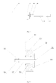
- the microwave feeding assembly 45 includes a mounting tube 56, a ceramic ring 57, a tube case 58 and an antenna 51.
- An end of the ceramic ring 57 is connected with the mounting tube 56, and the tube case 58 is connected with the other end of the ceramic ring 57.
- a first end (i.e. a right end in Fig. 4 ) of the antenna 51 is connected with the semiconductor power source 42, and a second end (i.e. a left end in Fig. 4 ) of the antenna 51 is extended through the tube case 58, the ceramic ring 57 and the mounting tube 56 sequentially into the rectangular wave guide 27.
- the antenna 51 converts a microwave of a mode of TE11 output by the semiconductor power plate 30 into a microwave of a mode of TE10 adaptive to microwave heating, and feeds the microwave of a mode of TE10 into the chamber body 26.
- an antenna cap 55 is fitted over an end (i.e. a left end in Fig. 4 ) of the mounting tube 56 adjacent to the rectangular wave guide 27, and the microwave feeding assembly 45 further includes a bottom plate 54, a first fixing ring 52 and a second fixing ring 53.
- the bottom plate 54 is mounted on the rectangular wave guide 27, the ceramic ring 57 is mounted on one side (i.e. a left side in Fig. 4 ) of the bottom plate 54, and the tube case 58 is mounted on the other side (i.e. a right side in Fig. 4 ) of the bottom plate 54.
- the first fixing ring 52 is mounted on the semiconductor power source 42, and the second fixing ring 53 is fitted over the tube case 58 and connected with the bottom plate 54 and the first fixing ring 52.
- first fixing ring 52 and the second fixing ring 53 may be fixed together via a bolt.
- the bolt passes through a through hole in the second fixing ring 53, and is screwed into a threaded hole in the first fixing ring 52, so as to achieve the connection between the first fixing ring 52 and the second fixing ring 53.
- a filler such as polytetrafluoroethylene may be filled in a space where the antenna 51 passes through.
- a blocking cover 59 is disposed on a right side of the first fixing ring 52 for stopping the first fixing ring 52 and the filler.
- the antenna 51 converts the microwave of a mode of TE11 output by the semiconductor power plate 30 into the microwave of a mode of TE10 adaptive to microwave heating, and feeds the microwave of a mode of TE10 into the chamber body 26 via the rectangular wave guide 27, such that the microwave feeding structure is simple in structure and low in cost. Therefore, the microwave oven having the magnetron tube in the related art may be modified so as to obtain the semiconductor microwave oven, without making modifications on other structures of the microwave oven in the related art, thus reducing the cost.
- the microwave feeding assembly includes a bottom plate 54, a first fixing ring 52 and a probe 64.
- the bottom plate 54 is mounted on the rectangular wave guide 27.
- the first fixing ring 52 is connected between the bottom plate 54 and the semiconductor power source 42.
- the probe 64 passes through the bottom plate 54 and the first fixing ring 52 sequentially, a first end (i.e. a right end in Fig. 6 ) of the probe 64 is connected with the semiconductor power source 42, and a second end (i.e. a left end in Fig. 6 ) of the probe 64 is connected with the rectangular wave guide 27.
- the probe 64 converts a microwave of a mode of TE11 output by a semiconductor power plate 30 into a microwave of a mode of TE10 adaptive to microwave heating, and feeds the microwave of a mode of TE10 into the chamber body 26.
- the first end of the probe 64 may be connected with a micro-strip line of the semiconductor power source 42 directly or via a coaxial transmission cable 46. If the first end of the probe 64 is connected with the micro-strip line of the semiconductor power source 42 via the coaxial transmission cable 46, an N-type connector is mounted on the semiconductor power plate 30 for converting a micro-strip output into a coaxial output, and the coaxial transmission cable 46 is connected with the semiconductor power plate 30 via the N-type connector.
- polytetrafluoroethylene may also be filled in a space of the bottom plate 54 and the first fixing ring 52 where the antenna 51 passes through, and the space is blocked by a blocking cover 59.
- microwave feeding structure according to the second embodiment of the present invention may be the same as those according to the first embodiment of the present invention, and will not be repeatedly described here.
- the microwave feeding structure according to the second embodiment of the present invention is more simple in structure and lower in cost, and may feed the microwave generated by the semiconductor power source into the chamber body effectively.
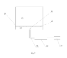
- the microwave feeding assembly of the microwave feeding structure includes an antenna 51.
- a first end (i.e. a right end in Fig. 7 ) of the antenna 51 is connected with the semiconductor power source 42, and a second end (i.e. a left end in Fig. 7 ) of the antenna 51 is extended into the chamber body 26. Therefore, the antenna 51 may conveniently convert a microwave of a mode of TE11 output by a semiconductor power plate 30 into a microwave of a mode of TE10 adaptive to microwave heating, and feed the microwave of a mode of TE10 into the chamber body 26.
- a ceramic plate 85 is disposed in the chamber body 26 and divides an interior of the chamber body 26 into a first chamber C1 and a second chamber C2, the second end of the antenna 51 is extended into the second chamber C2, and the first chamber C1 is used to accommodate food, thus avoiding the contamination of the antenna 51 resulting from the cooking of food.
- the antenna 51 may be connected with the semiconductor power plate 30 via a coaxial transmission cable 46.
- microwave feeding structure according to the third embodiment of the present invention may be the same as those according to the first and second embodiments of the present invention, and will not be described in detail here.
- the semiconductor microwave oven according to an embodiment of the present invention includes a chamber body 26, a semiconductor power source 42, a microwave feeding assembly and a power supply.
- the chamber body 26 has a door 25 for opening or closing an opening of the chamber body 26.
- the semiconductor power source 42 is configured to generate a microwave.
- the microwave feeding assembly is connected between the semiconductor power source 42 and the chamber body 26, so as to convert the microwave of a mode of TE11 output by the semiconductor power source 42 into a microwave of a mode of TE10 adaptive to microwave heating and to feed the microwave of a mode of TE10 into the chamber body 26, thus heating food in the chamber body 26.
- the power supply such as a direct current power supply 20 is connected with the semiconductor power source 42 for powering the semiconductor power source 42.
- the microwave feeding assembly of the semiconductor microwave oven may be the microwave feeding assembly described with reference to any one of the above embodiments, and other structures and operation of the semiconductor microwave oven is known to those skilled in the art and will not be described in detail here.
- the microwave generated by the semiconductor power source 42 may be fed into the chamber body 26 by means of the microwave feeding assembly, the microwave feeding structure is simple in structure and low in cost, and the semiconductor microwave oven is high in efficiency, simple in structure, low in cost and light in weight, and generates a large power density per unit volume.
Abstract
Description
- Embodiments of the present invention relate to a semiconductor microwave oven and a microwave feeding structure thereof.
- A magnetron microwave oven in the related art includes a magnetron, a transformer, a high-voltage capacitor, a high-voltage diode, a chamber body, a door and a control component. As shown in
Fig. 1 , a microwave generated by a magnetron tube 11' is fed into a chamber body 13' of a microwave oven via a rectangular wave guide 12', so as to heat food in the chamber body 13'. - A semiconductor microwave technology has been widely applied. A frequency band of the semiconductor microwave technology applied in the communication field is different from that applied in microwave heating field. The microwave output by a semiconductor power source has a mode of TE11 and an impedance of 50 Ω, and a microwave mode adaptive to microwave heating is TE10. In order to apply the semiconductor microwave technology to the microwave oven, there is a need for a microwave feeding structure for feeding a microwave output of a semiconductor power source into a chamber body of the microwave oven.
- The present invention seeks to solve at least one of the problems existing in the related art to at least some extent.
- An object of the present invention is to provide a microwave feeding structure for a semiconductor microwave oven, which is simple in structure, flexible to operate, and wide in application range.
- Another object of the present invention is to provide a semiconductor microwave oven having the abovementioned microwave feeding structure.
- A microwave feeding structure for a semiconductor microwave oven according to embodiments of a first aspect of the present invention includes: a chamber body having a door; a semiconductor power source configured to generate a microwave; and a microwave feeding assembly connected between the semiconductor power source and the chamber body, and configured to feed the microwave generated by the semiconductor power source into the chamber body and to convert a first microwave mode output by the semiconductor power source into a second microwave mode adaptive to microwave heating.
- The microwave feeding structure for the semiconductor microwave oven according to embodiments of the present invention may feed the microwave generated by the semiconductor power source into the chamber body, and convert a microwave of a mode of TE11 output by the semiconductor power source into a microwave of a mode of TE10 adaptive to microwave heating. Moreover, the microwave feeding structure is simple and reasonable in structure, flexible to operate, and wide in application range.
- In some embodiments, the semiconductor power source includes: a semiconductor power plate connected with the microwave feeding assembly; a shield disposed above the semiconductor power plate; and a radiator attached on a bottom surface of the semiconductor power plate.
- The microwave feeding structure according to embodiments of the present invention further includes a rectangular wave guide connected with the chamber body, wherein the microwave feeding assembly is connected between the semiconductor power source and the rectangular wave guide.
- In some embodiments, the microwave feeding assembly includes: a mounting tube; a ceramic ring connected with the mounting tube; a tube case connected with the ceramic ring; and an antenna defining a first end connected with the semiconductor power source and a second end extended through the tube case, the ceramic ring and the mounting tube sequentially into the rectangular wave guide.
- In some embodiments, an antenna cap is fitted over an end of the mounting tube adjacent to the rectangular wave guide, and the microwave feeding assembly further includes: a bottom plate mounted on the rectangular wave guide, the ceramic ring being mounted on one side of the bottom plate, and the tube case being mounted on the other side of the bottom plate; a first fixing ring mounted on the semiconductor power source; and a second fixing ring fitted over the tube case and connected with the bottom plate and the first fixing ring.
- In some embodiments, the microwave feeding assembly includes: a bottom plate mounted on the rectangular wave guide; a first fixing ring connected between the bottom plate and the semiconductor power source; and a probe passing through the bottom plate and the first fixing ring, and defining a first end connected with the semiconductor power source and a second end extended into the rectangular wave guide.
- In some embodiments, the first end of the probe is connected with a micro-strip line of the semiconductor power source directly or via a coaxial transmission cable.
- In some embodiments, the microwave feeding assembly includes an antenna defining a first end connected with the semiconductor power source via a coaxial transmission cable and a second end extended into the chamber body.
- In some embodiments, a ceramic plate is disposed in the chamber body and divides an interior of the chamber body into a first chamber and a second chamber, the second end of the antenna being extended into the second chamber.
- A semiconductor microwave oven according to embodiments of a second aspect of the present invention includes: a chamber body having a door; a semiconductor power source configured to generate a microwave; a microwave feeding assembly connected between the semiconductor power source and the chamber body, and configured to feed the microwave generated by the semiconductor power source into the chamber body and to convert a first microwave mode output by the semiconductor power source into a second microwave mode adaptive to microwave heating; and a power supply connected with the semiconductor power source.
- With the semiconductor microwave oven according to embodiments of the present invention, the microwave is generated by the semiconductor power source, and a microwave of a mode of TE11 output by the semiconductor power source is converted into a microwave of a mode of TE10 adaptive to microwave heating by means of the microwave feeding assembly, such that the semiconductor microwave oven is high in efficiency, simple in structure, low in cost and light in weight, and generates a large power density per unit volume.
- In some embodiments, the semiconductor power source includes: a semiconductor power plate connected with the microwave feeding assembly; a shield disposed above the semiconductor power plate; and a radiator attached on a bottom surface of the semiconductor power plate.
- The semiconductor microwave oven according to according to embodiments of the present invention further includes a rectangular wave guide connected with the chamber body, wherein the microwave feeding assembly is connected between the semiconductor power source and the rectangular wave guide.
- In some embodiments, the microwave feeding assembly includes: a mounting tube; a ceramic ring connected with the mounting tube; a tube case connected with the ceramic ring; and an antenna defining a first end connected with the semiconductor power source and a second end extended through the tube case, the ceramic ring and the mounting tube sequentially into the rectangular wave guide.
- In some embodiments, an antenna cap is fitted over an end of the mounting tube adjacent to the rectangular wave guide, and the microwave feeding assembly further includes: a bottom plate mounted on the rectangular wave guide, the ceramic ring being mounted on one side of the bottom plate, and the tube case being mounted on the other side of the bottom plate; a first fixing ring mounted on the semiconductor power source; and a second fixing ring fitted over the tube case and connected with the bottom plate and the first fixing ring.
- In some embodiments, the microwave feeding assembly includes: a bottom plate mounted on the rectangular wave guide; a first fixing ring connected between the bottom plate and the semiconductor power source; and a probe passing through the bottom plate and the first fixing ring, and defining a first end connected with the semiconductor power source and a second end extended into the rectangular wave guide.
- In some embodiments, the first end of the probe is connected with a micro-strip line of the semiconductor power source directly or via a coaxial transmission cable.
- In some embodiments, the microwave feeding assembly includes an antenna defining a first end connected with the semiconductor power source via a coaxial transmission cable and a second end extended into the chamber body.
- In some embodiments, a ceramic plate is disposed in the chamber body and divides an interior of the chamber body into a first chamber and a second chamber, the first end of the antenna is connected with the semiconductor power source, and the second end of the antenna is extended into the second chamber.
-
-
Fig. 1 is schematic view of a microwave oven having a magnetron tube in the related art; -
Fig. 2 is a schematic exploded view of a semiconductor microwave oven according to a first embodiment of the present invention; -
Fig. 3 is a schematic side view of the semiconductor microwave oven according to the first embodiment of the present invention; -
Fig. 4 is a schematic partial view of a microwave feeding assembly of the semiconductor microwave oven according to the first embodiment of the present invention, in which the microwave feeding assembly is similar to a magnetron output assembly of a microwave oven in the related art; -
Fig. 5 is a schematic side view of a semiconductor microwave oven according to a second embodiment of the present invention; -
Fig. 6 is a schematic partial view of a microwave feeding assembly of the semiconductor microwave oven according to the second embodiment of the present invention; -
Fig. 7 is a schematic view of a semiconductor microwave oven according to a third embodiment of the present invention; in which:- 20
- direct current power supply;
- 24
- cooling fan;
- 25
- door;
- 26
- chamber body;
- 27
- rectangular wave guide;
- 30
- semiconductor power plate;
- 31
- shield;
- 33
- radiator;
- 42
- semiconductor power source;
- 45
- magnetron output assembly;
- 46
- coaxial transmission line;
- 51
- antenna;
- 52
- first fixing ring;
- 53
- second fixing ring;
- 54
- bottom plate;
- 55
- antenna cap;
- 56
- mounting tube;
- 57
- ceramic ring;
- 58
- tube case;
- 59
- blocking cover;
- 64
- probe;
- 85
- ceramic plate.
- In the specification, it is to be understood that terms such as "central," "longitudinal," "lateral," "length," "width," "thickness," "upper," "lower," "front," "rear," "left," "right," "vertical," "horizontal," "top," "bottom," "inner," "outer," "clockwise," and "counterclockwise" should be construed to refer to the orientation as then described or as shown in the drawings under discussion. These relative terms are for convenience of description and do not require that the present invention be constructed or operated in a particular orientation.
- In addition, terms such as "first" and "second" are used herein for purposes of description and are not intended to indicate or imply relative importance or significance or to imply the number of indicated technical features. Thus, the feature defined with "first" and "second" may comprise one or more of this feature. In the description of the present invention, "a plurality of" means two or more than two, unless specified otherwise.
- In the present invention, unless specified or limited otherwise, the terms "mounted," "connected," "coupled," "fixed" and the like are used broadly, and may be, for example, fixed connections, detachable connections, or integral connections; may also be mechanical or electrical connections; may also be direct connections or indirect connections via intervening structures; may also be inner communications of two elements, which can be understood by those skilled in the art according to specific situations.
- In the present invention, unless specified or limited otherwise, a structure in which a first feature is "on" or "below" a second feature may include an embodiment in which the first feature is in direct contact with the second feature, and may also include an embodiment in which the first feature and the second feature are not in direct contact with each other, but are contacted via an additional feature formed therebetween. Furthermore, a first feature "on," "above," or "on top of" a second feature may include an embodiment in which the first feature is right or obliquely "on," "above," or "on top of" the second feature, or just means that the first feature is at a height higher than that of the second feature; while a first feature "below," "under," or "on bottom of" a second feature may include an embodiment in which the first feature is right or obliquely "below," "under," or "on bottom of" the second feature, or just means that the first feature is at a height lower than that of the second feature.
- A microwave feeding structure for a semiconductor microwave oven according to an embodiment of the present invention will be described below with reference to the drawings.
- As shown in
Figs. 2-7 , the microwave feeding structure for the semiconductor microwave oven according to an embodiment of the present invention includes achamber body 26, asemiconductor power source 42 and a microwave feeding assembly. Thechamber body 26 has adoor 25 for opening or closing an opening of thechamber body 26. Thesemiconductor power source 42 is configured to generate a microwave. The microwave feeding assembly is connected with thesemiconductor power source 42 and thechamber body 26, so as to feed the microwave generated by thesemiconductor power source 42 into thechamber body 26 and to convert a first microwave mode output by thesemiconductor power source 42 into a second microwave mode adaptive to microwave heating, thus heating food in thechamber body 26. A directcurrent power supply 20 is connected with thesemiconductor power source 42 for powering thesemiconductor power source 42. - The microwave feeding structure for the semiconductor microwave oven according to embodiments of the present invention may feed the microwave generated by the
semiconductor power source 42 into thechamber body 26, that is, a microwave of a mode of TE11 output by thesemiconductor power source 42 is converted into a microwave of a mode of TE10 adaptive to microwave heating by means of the microwave feeding assembly. Moreover, since the microwave is generated by thesemiconductor power source 42, the microwave oven is high in heating efficiency, simple in structure, low in cost and light in weight, and generates a large power density per unit volume; and the microwave feeding structure is simple in structure, flexible to operate, and wide in application range. - In some particular embodiments, the
semiconductor power source 42 includes a semiconductor power plate 30, ashield 31 and aradiator 33. Theshield 31 is disposed above the semiconductor power plate 30 for shielding the semiconductor power plate 30. The semiconductor power plate 30 is connected with the microwave feeding assembly. Theradiator 33 is attached on a bottom surface of the semiconductor power plate 30 for radiating heat generated by the semiconductor power plate 30. A coolingfan 24 is disposed in thechamber body 26 for radiating heat. - As described above, with the
semiconductor power source 42, the microwave generated by the semiconductor power plate 30 is fed into thechamber body 26, and a microwave of a mode of TE11 output by thesemiconductor power source 42 is converted into a microwave of a mode of TE10 adaptive to microwave heating by means of the microwave feeding structure, thus achieving the semiconductor microwave heating. - It would be appreciated by those skilled in the art that the semiconductor power plate 30 is provided with an LDMOS (laterally diffused metal oxide semiconductor) transistor, a biasing and control circuit, a power combiner, and a power detection and control circuit. A switching power supply, an accumulator or a charger is disposed between the
semiconductor power source 42 and an external alternating current power supply for transforming a voltage. The biasing and control circuit includes a circuit for detecting the output power of the semiconductor power source, a circuit for detecting the reflection power of the semiconductor power source, a turn-off signal circuit of the semiconductor power source, a direct current + input circuit of the semiconductor power source, and a direct current - input circuit of the semiconductor power source. A desired voltage of the semiconductor power source is direct current 0-32 V. The microwave output power of an excitation source may be adjusted by adjusting the input voltage, thus realizing stepless adjustment of the power of a semiconductor microwave oven. This would be appreciated by those skilled in the art, and will not be described in detail here. - The operation principle of the semiconductor power plate 30 is as follows: a certain number of LDMOS transistors with a certain power generate a microwave with a frequency of 2450MHz±50MHz via a self-oscillation circuit. The frequency may also be varied by adjusting the variable capacitance of the self-oscillation circuit of the LDMOS transistors. Depending on the standing wave ratio of the chamber body under practical conditions (e.g., the thickness of food, a heating state), a frequency with a minimum standing wave is selected from a range of 2400 MHz to 2500 MHz for heating.
- Particular embodiments of the microwave feeding structure for the semiconductor microwave oven according to the present invention will be described below with reference to the drawings.
- Referring to
Figs. 2-4 , the microwave feeding structure for the semiconductor microwave oven according to the first embodiment of the present invention includes achamber body 26 having adoor 25, asemiconductor power source 42, arectangular wave guide 27 and amicrowave feeding assembly 45. Therectangular wave guide 27 is mounted on thechamber body 26, and a semiconductor power plate 30 of thesemiconductor power source 42 may be connected with themicrowave feeding assembly 45 directly or via acoaxial transmission cable 46. If the semiconductor power plate 30 of thesemiconductor power source 42 is connected with themicrowave feeding assembly 45 via thecoaxial transmission cable 46, an N-type connector is mounted on the semiconductor power plate 30 for converting a micro-strip output into a coaxial output, and thecoaxial transmission cable 46 is connected with the semiconductor power plate 30 via the N-type connector. - A
radiator 33 is closely attached to a bottom surface of the semiconductor power plate 30, a shield 21 is located between the semiconductor power plate 30 and a shell of the semiconductor microwave oven, and themicrowave feeding assembly 45 is connected with therectangular wave guide 27, such that the microwave generated by thesemiconductor power source 42 is fed into thechamber body 26 via themicrowave feeding assembly 45 and therectangular wave guide 27. - In this embodiment, the
microwave feeding assembly 45 is similar to a magnetron output assembly of a microwave oven having a magnetron tube in the related art, such that the microwave oven having the magnetron tube in the related art may be conveniently modified. Specifically, the magnetron tube of the microwave oven in the related art is replaced with thesemiconductor power source 42, and the magnetron output assembly is appropriately modified so as to obtain the semiconductor microwave oven, without making other modifications on the microwave oven in the related art, thus reducing the cost. - As shown in
Fig. 4 , in this embodiment, themicrowave feeding assembly 45 includes a mountingtube 56, aceramic ring 57, atube case 58 and anantenna 51. An end of theceramic ring 57 is connected with the mountingtube 56, and thetube case 58 is connected with the other end of theceramic ring 57. A first end (i.e. a right end inFig. 4 ) of theantenna 51 is connected with thesemiconductor power source 42, and a second end (i.e. a left end inFig. 4 ) of theantenna 51 is extended through thetube case 58, theceramic ring 57 and the mountingtube 56 sequentially into therectangular wave guide 27. Theantenna 51 converts a microwave of a mode of TE11 output by the semiconductor power plate 30 into a microwave of a mode of TE10 adaptive to microwave heating, and feeds the microwave of a mode of TE10 into thechamber body 26. - In one example, as shown in
Fig. 4 , anantenna cap 55 is fitted over an end (i.e. a left end inFig. 4 ) of the mountingtube 56 adjacent to therectangular wave guide 27, and themicrowave feeding assembly 45 further includes abottom plate 54, afirst fixing ring 52 and asecond fixing ring 53. Thebottom plate 54 is mounted on therectangular wave guide 27, theceramic ring 57 is mounted on one side (i.e. a left side inFig. 4 ) of thebottom plate 54, and thetube case 58 is mounted on the other side (i.e. a right side inFig. 4 ) of thebottom plate 54. Thefirst fixing ring 52 is mounted on thesemiconductor power source 42, and thesecond fixing ring 53 is fitted over thetube case 58 and connected with thebottom plate 54 and thefirst fixing ring 52. - Particularly, the
first fixing ring 52 and thesecond fixing ring 53 may be fixed together via a bolt. Specifically, the bolt passes through a through hole in thesecond fixing ring 53, and is screwed into a threaded hole in thefirst fixing ring 52, so as to achieve the connection between thefirst fixing ring 52 and thesecond fixing ring 53. - As shown in
Fig. 4 , a filler such as polytetrafluoroethylene may be filled in a space where theantenna 51 passes through. A blockingcover 59 is disposed on a right side of thefirst fixing ring 52 for stopping thefirst fixing ring 52 and the filler. - With the microwave feeding structure according to the first embodiment of the present invention, the
antenna 51 converts the microwave of a mode of TE11 output by the semiconductor power plate 30 into the microwave of a mode of TE10 adaptive to microwave heating, and feeds the microwave of a mode of TE10 into thechamber body 26 via therectangular wave guide 27, such that the microwave feeding structure is simple in structure and low in cost. Therefore, the microwave oven having the magnetron tube in the related art may be modified so as to obtain the semiconductor microwave oven, without making modifications on other structures of the microwave oven in the related art, thus reducing the cost. - Referring to
Figs. 5-6 , in the second embodiment of the present invention, the microwave feeding assembly includes abottom plate 54, afirst fixing ring 52 and aprobe 64. Thebottom plate 54 is mounted on therectangular wave guide 27. Thefirst fixing ring 52 is connected between thebottom plate 54 and thesemiconductor power source 42. Theprobe 64 passes through thebottom plate 54 and thefirst fixing ring 52 sequentially, a first end (i.e. a right end inFig. 6 ) of theprobe 64 is connected with thesemiconductor power source 42, and a second end (i.e. a left end inFig. 6 ) of theprobe 64 is connected with therectangular wave guide 27. Theprobe 64 converts a microwave of a mode of TE11 output by a semiconductor power plate 30 into a microwave of a mode of TE10 adaptive to microwave heating, and feeds the microwave of a mode of TE10 into thechamber body 26. - Alternatively, the first end of the
probe 64 may be connected with a micro-strip line of thesemiconductor power source 42 directly or via acoaxial transmission cable 46. If the first end of theprobe 64 is connected with the micro-strip line of thesemiconductor power source 42 via thecoaxial transmission cable 46, an N-type connector is mounted on the semiconductor power plate 30 for converting a micro-strip output into a coaxial output, and thecoaxial transmission cable 46 is connected with the semiconductor power plate 30 via the N-type connector. - As shown in
Fig. 6 , polytetrafluoroethylene may also be filled in a space of thebottom plate 54 and thefirst fixing ring 52 where theantenna 51 passes through, and the space is blocked by a blockingcover 59. - Other structures and operation of the microwave feeding structure according to the second embodiment of the present invention may be the same as those according to the first embodiment of the present invention, and will not be repeatedly described here.
- The microwave feeding structure according to the second embodiment of the present invention is more simple in structure and lower in cost, and may feed the microwave generated by the semiconductor power source into the chamber body effectively.
- Referring to
Fig. 7 , in the third embodiment of the present invention, the microwave feeding assembly of the microwave feeding structure includes anantenna 51. A first end (i.e. a right end inFig. 7 ) of theantenna 51 is connected with thesemiconductor power source 42, and a second end (i.e. a left end inFig. 7 ) of theantenna 51 is extended into thechamber body 26. Therefore, theantenna 51 may conveniently convert a microwave of a mode of TE11 output by a semiconductor power plate 30 into a microwave of a mode of TE10 adaptive to microwave heating, and feed the microwave of a mode of TE10 into thechamber body 26. - In some embodiments, a
ceramic plate 85 is disposed in thechamber body 26 and divides an interior of thechamber body 26 into a first chamber C1 and a second chamber C2, the second end of theantenna 51 is extended into the second chamber C2, and the first chamber C1 is used to accommodate food, thus avoiding the contamination of theantenna 51 resulting from the cooking of food. - Alternatively, the
antenna 51 may be connected with the semiconductor power plate 30 via acoaxial transmission cable 46. - Other structures and operation of the microwave feeding structure according to the third embodiment of the present invention may be the same as those according to the first and second embodiments of the present invention, and will not be described in detail here.
- The microwave feeding structure according to the third embodiment of the present invention is more simple in structure and lower in cost
- The semiconductor microwave oven according to an embodiment of the present invention will be described below. The semiconductor microwave oven according to an embodiment of the present invention includes a
chamber body 26, asemiconductor power source 42, a microwave feeding assembly and a power supply. Thechamber body 26 has adoor 25 for opening or closing an opening of thechamber body 26. Thesemiconductor power source 42 is configured to generate a microwave. The microwave feeding assembly is connected between thesemiconductor power source 42 and thechamber body 26, so as to convert the microwave of a mode of TE11 output by thesemiconductor power source 42 into a microwave of a mode of TE10 adaptive to microwave heating and to feed the microwave of a mode of TE10 into thechamber body 26, thus heating food in thechamber body 26. The power supply such as a directcurrent power supply 20 is connected with thesemiconductor power source 42 for powering thesemiconductor power source 42. - The microwave feeding assembly of the semiconductor microwave oven according to an embodiment of the present invention may be the microwave feeding assembly described with reference to any one of the above embodiments, and other structures and operation of the semiconductor microwave oven is known to those skilled in the art and will not be described in detail here.
- With the semiconductor microwave oven according to embodiments of the present invention, the microwave generated by the
semiconductor power source 42 may be fed into thechamber body 26 by means of the microwave feeding assembly, the microwave feeding structure is simple in structure and low in cost, and the semiconductor microwave oven is high in efficiency, simple in structure, low in cost and light in weight, and generates a large power density per unit volume. - Reference throughout this specification to "an embodiment," "some embodiments," "one embodiment," "another example," "an example," "a specific example," or "some examples," means that a particular feature, structure, material, or characteristic described in connection with the embodiment or example is included in at least one embodiment or example of the present invention. Thus, the appearances of the phrases such as "in some embodiments," "in one embodiment," "in an embodiment," "in another example," "in an example," "in a specific example," or "in some examples," in various places throughout this specification are not necessarily referring to the same embodiment or example of the present invention. Furthermore, the particular features, structures, materials, or characteristics may be combined in any suitable manner in one or more embodiments or examples.
- Although explanatory embodiments have been shown and described, it would be appreciated by those skilled in the art that the above embodiments cannot be construed to limit the present invention, and changes, alternatives, and modifications can be made in the embodiments without departing from spirit, principles and scope of the present invention.
Claims (18)
- A microwave feeding structure for a semiconductor microwave oven, comprising:a chamber body (26) having a door (25);a semiconductor power source (42) configured to generate a microwave; anda microwave feeding assembly connected between the semiconductor power source (42) and the chamber body (26), and configured to feed the microwave generated by the semiconductor power source (42) into the chamber body (26) and to convert a first microwave mode output by the semiconductor power source (42) into a second microwave mode adaptive to microwave heating.
- The microwave feeding structure according to claim 1, wherein the semiconductor power source (42) comprises:a semiconductor power plate (30) connected with the microwave feeding assembly;a shield (31) disposed above the semiconductor power plate (30); anda radiator (33) attached on a bottom surface of the semiconductor power plate (30).
- The microwave feeding structure according to claim 1 or 2, further comprising:a rectangular wave guide (27) connected with the chamber body (26),wherein the microwave feeding assembly is connected between the semiconductor power source (42) and the rectangular wave guide (27).
- The microwave feeding structure according to claim 3, wherein the microwave feeding assembly comprises:a mounting tube (56);a ceramic ring (57) connected with the mounting tube (56);a tube case (58) connected with the ceramic ring (57); andan antenna (51) defining a first end connected with the semiconductor power source (42) and a second end extended through the tube case (58), the ceramic ring (57) and the mounting tube (56) sequentially into the rectangular wave guide (27).
- The microwave feeding structure according to claim 4, wherein an antenna cap (55) is fitted over an end of the mounting tube (56) adjacent to the rectangular wave guide (27), and
wherein the microwave feeding assembly further comprises:a bottom plate (54) mounted on the rectangular wave guide (27), the ceramic ring being mounted on one side of the bottom plate, and the tube case being mounted on the other side of the bottom plate;a first fixing ring (52) mounted on the semiconductor power source (42); anda second fixing ring (53) fitted over the tube case (58) and connected with the bottom plate (54) and the first fixing ring (52). - The microwave feeding structure according to claim 3, wherein the microwave feeding assembly comprises:a bottom plate (54) mounted on the rectangular wave guide (27);a first fixing ring (52) connected between the bottom plate (54) and the semiconductor power source (42); anda probe (64) passing through the bottom plate (54) and the first fixing ring (52), and defining a first end connected with the semiconductor power source (42) and a second end extended into the rectangular wave guide (27).
- The microwave feeding structure according to claim 6, wherein the first end of the probe (64) is connected with a micro-strip line of the semiconductor power source (42) directly or via a coaxial transmission cable (46).
- The microwave feeding structure according to claim 1 or 2, wherein the microwave feeding assembly comprises an antenna (51) defining a first end connected with the semiconductor power source (42) via a coaxial transmission cable (46) and a second end extended into the chamber body (26).
- The microwave feeding structure according to claim 8, wherein a ceramic plate (85) is disposed in the chamber body (26) and divides an interior of the chamber body (26) into a first chamber and a second chamber, the second end of the antenna (51) being extended into the second chamber.
- A semiconductor microwave oven, comprising:a chamber body (26) having a door (25);a semiconductor power source (42) configured to generate a microwave;a microwave feeding assembly connected between the semiconductor power source (42) and the chamber body (26), and configured to feed the microwave generated by the semiconductor power source into the chamber body and to convert a first microwave mode output by the semiconductor power source (42) into a second microwave mode adaptive to microwave heating; anda power supply (20) connected with the semiconductor power source (42).
- The semiconductor microwave oven according to claim 11, wherein the semiconductor power source (42) comprises:a semiconductor power plate (30) connected with the microwave feeding assembly;a shield (31) disposed above the semiconductor power plate (30); anda radiator (33) attached on a bottom surface of the semiconductor power plate (30).
- The semiconductor microwave oven according to claim 10 or 11, further comprising:a rectangular wave guide (27) connected with the chamber body (26),wherein the microwave feeding assembly is connected between the semiconductor power source (42) and the rectangular wave guide (27).
- The semiconductor microwave oven according to claim 12, wherein the microwave feeding assembly comprises:a mounting tube (56);a ceramic ring (57) connected with the mounting tube (56);a tube case (58) connected with the ceramic ring (57); andan antenna (51) defining a first end connected with the semiconductor power source (42) and a second end extended through the tube case (58), the ceramic ring (57) and the mounting tube (56) sequentially into the rectangular wave guide (27).
- The semiconductor microwave oven according to claim 13, wherein an antenna cap (55) is fitted over an end of the mounting tube (56) adjacent to the rectangular wave guide, and the microwave feeding assembly further comprises:a bottom plate (54) mounted on the rectangular wave guide, the ceramic ring being mounted on one side of the bottom plate, and the tube case being mounted on the other side of the bottom plate;a first fixing ring (52) mounted on the semiconductor power source (42); anda second fixing ring (53) fitted over the tube case (58) and connected with the bottom plate and the first fixing ring.
- The semiconductor microwave oven according to claim 12, wherein the microwave feeding assembly comprises:a bottom plate (54) mounted on the rectangular wave guide (27);a first fixing ring (52) connected between the bottom plate (54) and the semiconductor power source (42); anda probe (64) passing through the bottom plate (54) and the first fixing ring (52), and defining a first end connected with the semiconductor power source (42) and a second end extended into the rectangular wave guide (27).
- The semiconductor microwave oven according to claim 16, wherein the first end of the probe (64) is connected with a micro-strip line of the semiconductor power source (42) directly or via a coaxial transmission cable (46).
- The semiconductor microwave oven according to claim 10 or 11, wherein the microwave feeding assembly comprises an antenna (51) defining a first end connected with the semiconductor power source (42) via a coaxial transmission cable (46) and a second end extended into the chamber body (26).
- The semiconductor microwave oven according to claim 17, wherein a ceramic plate (85) is disposed in the chamber body (26) and divides an interior of the chamber body (26) into a first chamber and a second chamber, the first end of the antenna (51) is connected with the semiconductor power source (42), and the second end of the antenna (51) is extended into the second chamber.
Applications Claiming Priority (2)
| Application Number | Priority Date | Filing Date | Title |
|---|---|---|---|
| CN201110339203.XA CN102374557B (en) | 2011-10-31 | 2011-10-31 | The microwave feed-in structure of semiconductor microwave oven |
| PCT/CN2012/081383 WO2013063985A1 (en) | 2011-10-31 | 2012-09-14 | Semiconductor microwave oven and microwave feeding structure thereof |
Publications (3)
| Publication Number | Publication Date |
|---|---|
| EP2778539A1 true EP2778539A1 (en) | 2014-09-17 |
| EP2778539A4 EP2778539A4 (en) | 2015-07-15 |
| EP2778539B1 EP2778539B1 (en) | 2016-12-21 |
Family
ID=45793556
Family Applications (1)
| Application Number | Title | Priority Date | Filing Date |
|---|---|---|---|
| EP12845045.9A Active EP2778539B1 (en) | 2011-10-31 | 2012-09-14 | Semiconductor microwave oven and microwave feeding structure thereof |
Country Status (5)
| Country | Link |
|---|---|
| US (1) | US10015846B2 (en) |
| EP (1) | EP2778539B1 (en) |
| KR (1) | KR101570015B1 (en) |
| CN (1) | CN102374557B (en) |
| WO (1) | WO2013063985A1 (en) |
Cited By (2)
| Publication number | Priority date | Publication date | Assignee | Title |
|---|---|---|---|---|
| EP3177109A1 (en) * | 2015-12-04 | 2017-06-07 | Electrolux Appliances Aktiebolag | Microwave oven |
| WO2018102151A1 (en) * | 2016-11-30 | 2018-06-07 | Illinois Tool Works Inc. | Apparatus and system for solid state oven electronics cooling |
Families Citing this family (21)
| Publication number | Priority date | Publication date | Assignee | Title |
|---|---|---|---|---|
| CN102374557B (en) * | 2011-10-31 | 2016-08-03 | 广东美的厨房电器制造有限公司 | The microwave feed-in structure of semiconductor microwave oven |
| EP2654066B1 (en) * | 2012-04-20 | 2019-10-23 | NXP USA, Inc. | Microwave adaptors and related oscillator systems |
| CN103378390B (en) * | 2012-04-20 | 2018-04-10 | 恩智浦美国有限公司 | The oscilator system of microwave adapter and correlation |
| CN102679417B (en) * | 2012-05-21 | 2014-06-11 | 广东美的厨房电器制造有限公司 | Semiconductor microwave oven |
| CN102767855B (en) * | 2012-07-18 | 2015-12-16 | 广东格兰仕微波炉电器制造有限公司 | The syndeton of micro-wave oven and semiconductor microwave generator and antenna |
| CN102769951B (en) * | 2012-07-18 | 2015-03-11 | 广东格兰仕微波炉电器制造有限公司 | Semiconductor microwave oven and semiconductor microwave generator connecting structure for same |
| CN102767854B (en) * | 2012-07-18 | 2015-03-25 | 广东格兰仕微波炉电器制造有限公司 | Microwave oven |
| CN102769952B (en) * | 2012-07-18 | 2015-03-11 | 广东格兰仕微波炉电器制造有限公司 | Semiconductor microwave oven and semiconductor microwave generator connecting structure for same |
| CN103851661B (en) * | 2012-12-06 | 2016-08-17 | 广东美的厨房电器制造有限公司 | Semiconductor microwave oven |
| CN103512060A (en) * | 2013-09-13 | 2014-01-15 | 无锡市佳信安科技有限公司 | Microwave radiation unit of semiconductor microwave oven |
| CN103912900A (en) * | 2014-03-20 | 2014-07-09 | 广东美的厨房电器制造有限公司 | Semiconductor microwave generator connection structure of microwave oven and microwave oven |
| CA2942672C (en) | 2014-03-20 | 2021-10-26 | Guangdong Midea Kitchen Appliances Manufacturing Co., Ltd. | Connection structure and input/output connection structure of semiconductor microwave generator for microwave oven, and microwave oven |
| JP2017525121A (en) * | 2014-05-28 | 2017-08-31 | グァンドン ミデア キッチン アプライアンシズ マニュファクチュアリング カンパニー リミテッド | Semiconductor microwave oven and semiconductor microwave source |
| CN104676675B (en) * | 2014-08-12 | 2017-05-03 | 广东美的厨房电器制造有限公司 | Microwave oven and exciter for microwave oven |
| CN105402787B (en) * | 2014-09-15 | 2017-10-24 | 广东美的厨房电器制造有限公司 | Micro-wave oven |
| DE102014226280B4 (en) | 2014-12-17 | 2019-06-13 | E.G.O. Elektro-Gerätebau GmbH | Microwave generator and microwave oven |
| CN104654381B (en) * | 2015-02-12 | 2017-08-04 | 广东美的厨房电器制造有限公司 | Semiconductor microwave oven and the semiconductor power source for micro-wave oven |
| CN104791858A (en) * | 2015-03-23 | 2015-07-22 | 广东美的厨房电器制造有限公司 | Microwave oven |
| CN105485732B (en) * | 2015-12-31 | 2018-02-16 | 广东美的厨房电器制造有限公司 | Micro-wave oven |
| DE102016221447A1 (en) | 2016-11-02 | 2018-05-03 | BSH Hausgeräte GmbH | Household cooking appliance |
| EP3448121B1 (en) * | 2017-08-23 | 2020-12-23 | Vorwerk & Co. Interholding GmbH | Microwave feed-in device on a microwave oven |
Family Cites Families (21)
| Publication number | Priority date | Publication date | Assignee | Title |
|---|---|---|---|---|
| US4336434A (en) * | 1980-08-15 | 1982-06-22 | General Electric Company | Microwave oven cavity excitation system employing circularly polarized beam steering for uniformity of energy distribution and improved impedance matching |
| CA1202090A (en) * | 1982-09-20 | 1986-03-18 | Hisashi Okatsuka | Microwave heating apparatus with solid state microwave oscillating device |
| DE3474888D1 (en) * | 1983-01-20 | 1988-12-01 | Matsushita Electric Ind Co Ltd | Frequency converter |
| US4999469A (en) * | 1990-04-02 | 1991-03-12 | Raytheon Company | Apparatus for microwave heating test coupons |
| JPH05152811A (en) * | 1991-11-25 | 1993-06-18 | Fujitsu General Ltd | Circular waveguide/square waveguide converter |
| US5874706A (en) * | 1996-09-26 | 1999-02-23 | Tokyo Electron Limited | Microwave plasma processing apparatus using a hybrid microwave having two different modes of oscillation or branched microwaves forming a concentric electric field |
| JP3368159B2 (en) * | 1996-11-20 | 2003-01-20 | 東京エレクトロン株式会社 | Plasma processing equipment |
| JP3847540B2 (en) | 2000-09-05 | 2006-11-22 | ニッテツ八幡エンジニアリング株式会社 | Pollution-free rust-proof coating composition |
| JP4087696B2 (en) | 2002-12-25 | 2008-05-21 | 日立協和エンジニアリング株式会社 | Microwave heating device |
| CN1764332A (en) | 2004-10-01 | 2006-04-26 | 精工爱普生株式会社 | High-frequency heating device, semiconductor manufacturing device, and light source device |
| KR100710036B1 (en) * | 2005-12-21 | 2007-04-20 | 주식회사 대우일렉트로닉스 | Connector for magnetron and coaxial cables and microwave oven using the same |
| JP4899595B2 (en) * | 2006-04-07 | 2012-03-21 | パナソニック株式会社 | Microwave generator |
| JP5116260B2 (en) * | 2006-06-19 | 2013-01-09 | パナソニック株式会社 | High frequency heating device |
| EP2205043B1 (en) | 2007-10-18 | 2017-01-25 | Panasonic Corporation | Microwave heating device |
| JP4542625B2 (en) * | 2008-05-13 | 2010-09-15 | パナソニック株式会社 | Spread spectrum high frequency heating equipment |
| CN102067723B (en) * | 2008-06-25 | 2013-05-01 | 松下电器产业株式会社 | Microwave heating device |
| JP5589306B2 (en) | 2009-05-20 | 2014-09-17 | パナソニック株式会社 | Heat treatment equipment |
| CN101979923A (en) * | 2010-11-17 | 2011-02-23 | 美的集团有限公司 | Microwave oven with a heat exchanger |
| CN102062424A (en) * | 2011-01-17 | 2011-05-18 | 广东格兰仕集团有限公司 | Microwave oven without magnetron |
| CN102374557B (en) | 2011-10-31 | 2016-08-03 | 广东美的厨房电器制造有限公司 | The microwave feed-in structure of semiconductor microwave oven |
| CN202303515U (en) * | 2011-10-31 | 2012-07-04 | 广东美的微波电器制造有限公司 | Microwave Feeding Structure of Semiconductor Microwave Oven |
-
2011
- 2011-10-31 CN CN201110339203.XA patent/CN102374557B/en active Active
-
2012
- 2012-09-14 WO PCT/CN2012/081383 patent/WO2013063985A1/en active Application Filing
- 2012-09-14 KR KR1020147014490A patent/KR101570015B1/en active IP Right Grant
- 2012-09-14 EP EP12845045.9A patent/EP2778539B1/en active Active
- 2012-09-14 US US14/355,270 patent/US10015846B2/en active Active
Cited By (6)
| Publication number | Priority date | Publication date | Assignee | Title |
|---|---|---|---|---|
| EP3177109A1 (en) * | 2015-12-04 | 2017-06-07 | Electrolux Appliances Aktiebolag | Microwave oven |
| WO2017093154A1 (en) * | 2015-12-04 | 2017-06-08 | Electrolux Appliances Aktiebolag | Microwave oven |
| US10841986B2 (en) | 2015-12-04 | 2020-11-17 | Electrolux Appliances Aktiebolag | Microwave oven |
| AU2016363364B2 (en) * | 2015-12-04 | 2021-09-09 | Electrolux Appliances Aktiebolag | Microwave oven |
| WO2018102151A1 (en) * | 2016-11-30 | 2018-06-07 | Illinois Tool Works Inc. | Apparatus and system for solid state oven electronics cooling |
| US10904959B2 (en) | 2016-11-30 | 2021-01-26 | Illinois Tool Works, Inc. | Apparatus and system for solid state oven electronics cooling |
Also Published As
| Publication number | Publication date |
|---|---|
| KR20140100944A (en) | 2014-08-18 |
| US20140305933A1 (en) | 2014-10-16 |
| EP2778539A4 (en) | 2015-07-15 |
| CN102374557B (en) | 2016-08-03 |
| US10015846B2 (en) | 2018-07-03 |
| WO2013063985A1 (en) | 2013-05-10 |
| CN102374557A (en) | 2012-03-14 |
| EP2778539B1 (en) | 2016-12-21 |
| KR101570015B1 (en) | 2015-11-17 |
Similar Documents
| Publication | Publication Date | Title |
|---|---|---|
| EP2778539B1 (en) | Semiconductor microwave oven and microwave feeding structure thereof | |
| US10356855B2 (en) | Microwave heating apparatus | |
| US9876481B2 (en) | Microwave processing device | |
| US20110290230A1 (en) | Door choke and cooking apparatus including the same | |
| EP3121519B1 (en) | Connection structure and input/output connection structure of semiconductor microwave generator for microwave oven, and microwave oven | |
| EP3384731B1 (en) | Microwave oven | |
| US20150170866A1 (en) | Magnetron and high-frequency heating apparatus having the same | |
| CN109921745B (en) | Side output type radio frequency resonance generator and insecticidal sterilization device | |
| JPH0787739A (en) | Switching power-supply apparatus | |
| CN106211406B (en) | Semiconductor microwave heating device | |
| TWI415331B (en) | Broadband antenna | |
| KR20200021067A (en) | Microwave System | |
| JP6867670B2 (en) | Microwave therapy device | |
| CN110831272B (en) | Microwave oven | |
| CN110741731A (en) | Microwave cooking appliance with patch antenna | |
| KR20190083953A (en) | Microwave System | |
| KR101742987B1 (en) | A cooking apparatus using microwave | |
| CN116826339A (en) | Coaxial waveguide conversion device, microwave device and communication device | |
| CN115379608A (en) | Microwave heating device | |
| JP5445155B2 (en) | Microwave heating device | |
| RU2061273C1 (en) | Microwave power input/output device for helical slow-wave structure | |
| KR102035810B1 (en) | Cooking appliance | |
| CN115604879A (en) | Microwave heating device | |
| KR20200021066A (en) | Microwave System | |
| KR20200026848A (en) | Microwave System |
Legal Events
| Date | Code | Title | Description |
|---|---|---|---|
| PUAI | Public reference made under article 153(3) epc to a published international application that has entered the european phase |
Free format text: ORIGINAL CODE: 0009012 |
|
| 17P | Request for examination filed |
Effective date: 20140530 |
|
| AK | Designated contracting states |
Kind code of ref document: A1 Designated state(s): AL AT BE BG CH CY CZ DE DK EE ES FI FR GB GR HR HU IE IS IT LI LT LU LV MC MK MT NL NO PL PT RO RS SE SI SK SM TR |
|
| DAX | Request for extension of the european patent (deleted) | ||
| RA4 | Supplementary search report drawn up and despatched (corrected) |
Effective date: 20150615 |
|
| RIC1 | Information provided on ipc code assigned before grant |
Ipc: H05B 6/64 20060101ALI20150609BHEP Ipc: H05B 6/80 20060101ALI20150609BHEP Ipc: F24C 7/02 20060101AFI20150609BHEP Ipc: H05B 6/68 20060101ALI20150609BHEP |
|
| GRAP | Despatch of communication of intention to grant a patent |
Free format text: ORIGINAL CODE: EPIDOSNIGR1 |
|
| RIC1 | Information provided on ipc code assigned before grant |
Ipc: H05B 6/68 20060101ALI20160622BHEP Ipc: F24C 7/02 20060101AFI20160622BHEP Ipc: H05B 6/80 20060101ALI20160622BHEP Ipc: H05B 6/64 20060101ALI20160622BHEP |
|
| INTG | Intention to grant announced |
Effective date: 20160715 |
|
| GRAS | Grant fee paid |
Free format text: ORIGINAL CODE: EPIDOSNIGR3 |
|
| GRAA | (expected) grant |
Free format text: ORIGINAL CODE: 0009210 |
|
| AK | Designated contracting states |
Kind code of ref document: B1 Designated state(s): AL AT BE BG CH CY CZ DE DK EE ES FI FR GB GR HR HU IE IS IT LI LT LU LV MC MK MT NL NO PL PT RO RS SE SI SK SM TR |
|
| REG | Reference to a national code |
Ref country code: GB Ref legal event code: FG4D |
|
| REG | Reference to a national code |
Ref country code: CH Ref legal event code: EP |
|
| REG | Reference to a national code |
Ref country code: IE Ref legal event code: FG4D |
|
| REG | Reference to a national code |
Ref country code: AT Ref legal event code: REF Ref document number: 855831 Country of ref document: AT Kind code of ref document: T Effective date: 20170115 |
|
| REG | Reference to a national code |
Ref country code: DE Ref legal event code: R096 Ref document number: 602012026953 Country of ref document: DE |
|
| PG25 | Lapsed in a contracting state [announced via postgrant information from national office to epo] |
Ref country code: LV Free format text: LAPSE BECAUSE OF FAILURE TO SUBMIT A TRANSLATION OF THE DESCRIPTION OR TO PAY THE FEE WITHIN THE PRESCRIBED TIME-LIMIT Effective date: 20161221 |
|
| REG | Reference to a national code |
Ref country code: LT Ref legal event code: MG4D |
|
| REG | Reference to a national code |
Ref country code: NL Ref legal event code: MP Effective date: 20161221 |
|
| PG25 | Lapsed in a contracting state [announced via postgrant information from national office to epo] |
Ref country code: LT Free format text: LAPSE BECAUSE OF FAILURE TO SUBMIT A TRANSLATION OF THE DESCRIPTION OR TO PAY THE FEE WITHIN THE PRESCRIBED TIME-LIMIT Effective date: 20161221 Ref country code: GR Free format text: LAPSE BECAUSE OF FAILURE TO SUBMIT A TRANSLATION OF THE DESCRIPTION OR TO PAY THE FEE WITHIN THE PRESCRIBED TIME-LIMIT Effective date: 20170322 Ref country code: NO Free format text: LAPSE BECAUSE OF FAILURE TO SUBMIT A TRANSLATION OF THE DESCRIPTION OR TO PAY THE FEE WITHIN THE PRESCRIBED TIME-LIMIT Effective date: 20170321 Ref country code: SE Free format text: LAPSE BECAUSE OF FAILURE TO SUBMIT A TRANSLATION OF THE DESCRIPTION OR TO PAY THE FEE WITHIN THE PRESCRIBED TIME-LIMIT Effective date: 20161221 |
|
| REG | Reference to a national code |
Ref country code: AT Ref legal event code: MK05 Ref document number: 855831 Country of ref document: AT Kind code of ref document: T Effective date: 20161221 |
|
| PG25 | Lapsed in a contracting state [announced via postgrant information from national office to epo] |
Ref country code: RS Free format text: LAPSE BECAUSE OF FAILURE TO SUBMIT A TRANSLATION OF THE DESCRIPTION OR TO PAY THE FEE WITHIN THE PRESCRIBED TIME-LIMIT Effective date: 20161221 Ref country code: HR Free format text: LAPSE BECAUSE OF FAILURE TO SUBMIT A TRANSLATION OF THE DESCRIPTION OR TO PAY THE FEE WITHIN THE PRESCRIBED TIME-LIMIT Effective date: 20161221 Ref country code: FI Free format text: LAPSE BECAUSE OF FAILURE TO SUBMIT A TRANSLATION OF THE DESCRIPTION OR TO PAY THE FEE WITHIN THE PRESCRIBED TIME-LIMIT Effective date: 20161221 |
|
| PG25 | Lapsed in a contracting state [announced via postgrant information from national office to epo] |
Ref country code: NL Free format text: LAPSE BECAUSE OF FAILURE TO SUBMIT A TRANSLATION OF THE DESCRIPTION OR TO PAY THE FEE WITHIN THE PRESCRIBED TIME-LIMIT Effective date: 20161221 |
|
| PG25 | Lapsed in a contracting state [announced via postgrant information from national office to epo] |
Ref country code: SK Free format text: LAPSE BECAUSE OF FAILURE TO SUBMIT A TRANSLATION OF THE DESCRIPTION OR TO PAY THE FEE WITHIN THE PRESCRIBED TIME-LIMIT Effective date: 20161221 Ref country code: CZ Free format text: LAPSE BECAUSE OF FAILURE TO SUBMIT A TRANSLATION OF THE DESCRIPTION OR TO PAY THE FEE WITHIN THE PRESCRIBED TIME-LIMIT Effective date: 20161221 Ref country code: RO Free format text: LAPSE BECAUSE OF FAILURE TO SUBMIT A TRANSLATION OF THE DESCRIPTION OR TO PAY THE FEE WITHIN THE PRESCRIBED TIME-LIMIT Effective date: 20161221 Ref country code: EE Free format text: LAPSE BECAUSE OF FAILURE TO SUBMIT A TRANSLATION OF THE DESCRIPTION OR TO PAY THE FEE WITHIN THE PRESCRIBED TIME-LIMIT Effective date: 20161221 Ref country code: IS Free format text: LAPSE BECAUSE OF FAILURE TO SUBMIT A TRANSLATION OF THE DESCRIPTION OR TO PAY THE FEE WITHIN THE PRESCRIBED TIME-LIMIT Effective date: 20170421 |
|
| PG25 | Lapsed in a contracting state [announced via postgrant information from national office to epo] |
Ref country code: BG Free format text: LAPSE BECAUSE OF FAILURE TO SUBMIT A TRANSLATION OF THE DESCRIPTION OR TO PAY THE FEE WITHIN THE PRESCRIBED TIME-LIMIT Effective date: 20170321 Ref country code: ES Free format text: LAPSE BECAUSE OF FAILURE TO SUBMIT A TRANSLATION OF THE DESCRIPTION OR TO PAY THE FEE WITHIN THE PRESCRIBED TIME-LIMIT Effective date: 20161221 Ref country code: PL Free format text: LAPSE BECAUSE OF FAILURE TO SUBMIT A TRANSLATION OF THE DESCRIPTION OR TO PAY THE FEE WITHIN THE PRESCRIBED TIME-LIMIT Effective date: 20161221 Ref country code: PT Free format text: LAPSE BECAUSE OF FAILURE TO SUBMIT A TRANSLATION OF THE DESCRIPTION OR TO PAY THE FEE WITHIN THE PRESCRIBED TIME-LIMIT Effective date: 20170421 Ref country code: AT Free format text: LAPSE BECAUSE OF FAILURE TO SUBMIT A TRANSLATION OF THE DESCRIPTION OR TO PAY THE FEE WITHIN THE PRESCRIBED TIME-LIMIT Effective date: 20161221 Ref country code: SM Free format text: LAPSE BECAUSE OF FAILURE TO SUBMIT A TRANSLATION OF THE DESCRIPTION OR TO PAY THE FEE WITHIN THE PRESCRIBED TIME-LIMIT Effective date: 20161221 Ref country code: BE Free format text: LAPSE BECAUSE OF FAILURE TO SUBMIT A TRANSLATION OF THE DESCRIPTION OR TO PAY THE FEE WITHIN THE PRESCRIBED TIME-LIMIT Effective date: 20161221 |
|
| REG | Reference to a national code |
Ref country code: DE Ref legal event code: R097 Ref document number: 602012026953 Country of ref document: DE |
|
| REG | Reference to a national code |
Ref country code: FR Ref legal event code: PLFP Year of fee payment: 6 |
|
| PLBE | No opposition filed within time limit |
Free format text: ORIGINAL CODE: 0009261 |
|
| STAA | Information on the status of an ep patent application or granted ep patent |
Free format text: STATUS: NO OPPOSITION FILED WITHIN TIME LIMIT |
|
| 26N | No opposition filed |
Effective date: 20170922 |
|
| PG25 | Lapsed in a contracting state [announced via postgrant information from national office to epo] |
Ref country code: DK Free format text: LAPSE BECAUSE OF FAILURE TO SUBMIT A TRANSLATION OF THE DESCRIPTION OR TO PAY THE FEE WITHIN THE PRESCRIBED TIME-LIMIT Effective date: 20161221 |
|
| PG25 | Lapsed in a contracting state [announced via postgrant information from national office to epo] |
Ref country code: SI Free format text: LAPSE BECAUSE OF FAILURE TO SUBMIT A TRANSLATION OF THE DESCRIPTION OR TO PAY THE FEE WITHIN THE PRESCRIBED TIME-LIMIT Effective date: 20161221 |
|
| REG | Reference to a national code |
Ref country code: CH Ref legal event code: PL |
|
| PG25 | Lapsed in a contracting state [announced via postgrant information from national office to epo] |
Ref country code: MC Free format text: LAPSE BECAUSE OF FAILURE TO SUBMIT A TRANSLATION OF THE DESCRIPTION OR TO PAY THE FEE WITHIN THE PRESCRIBED TIME-LIMIT Effective date: 20161221 |
|
| REG | Reference to a national code |
Ref country code: IE Ref legal event code: MM4A |
|
| PG25 | Lapsed in a contracting state [announced via postgrant information from national office to epo] |
Ref country code: LU Free format text: LAPSE BECAUSE OF NON-PAYMENT OF DUE FEES Effective date: 20170914 |
|
| PG25 | Lapsed in a contracting state [announced via postgrant information from national office to epo] |
Ref country code: IE Free format text: LAPSE BECAUSE OF NON-PAYMENT OF DUE FEES Effective date: 20170914 Ref country code: CH Free format text: LAPSE BECAUSE OF NON-PAYMENT OF DUE FEES Effective date: 20170930 Ref country code: LI Free format text: LAPSE BECAUSE OF NON-PAYMENT OF DUE FEES Effective date: 20170930 |
|
| PG25 | Lapsed in a contracting state [announced via postgrant information from national office to epo] |
Ref country code: MT Free format text: LAPSE BECAUSE OF NON-PAYMENT OF DUE FEES Effective date: 20170914 |
|
| REG | Reference to a national code |
Ref country code: FR Ref legal event code: PLFP Year of fee payment: 7 |
|
| PG25 | Lapsed in a contracting state [announced via postgrant information from national office to epo] |
Ref country code: HU Free format text: LAPSE BECAUSE OF FAILURE TO SUBMIT A TRANSLATION OF THE DESCRIPTION OR TO PAY THE FEE WITHIN THE PRESCRIBED TIME-LIMIT; INVALID AB INITIO Effective date: 20120914 |
|
| PG25 | Lapsed in a contracting state [announced via postgrant information from national office to epo] |
Ref country code: CY Free format text: LAPSE BECAUSE OF FAILURE TO SUBMIT A TRANSLATION OF THE DESCRIPTION OR TO PAY THE FEE WITHIN THE PRESCRIBED TIME-LIMIT Effective date: 20161221 |
|
| PG25 | Lapsed in a contracting state [announced via postgrant information from national office to epo] |
Ref country code: MK Free format text: LAPSE BECAUSE OF FAILURE TO SUBMIT A TRANSLATION OF THE DESCRIPTION OR TO PAY THE FEE WITHIN THE PRESCRIBED TIME-LIMIT Effective date: 20161221 |
|
| PG25 | Lapsed in a contracting state [announced via postgrant information from national office to epo] |
Ref country code: TR Free format text: LAPSE BECAUSE OF FAILURE TO SUBMIT A TRANSLATION OF THE DESCRIPTION OR TO PAY THE FEE WITHIN THE PRESCRIBED TIME-LIMIT Effective date: 20161221 |
|
| PG25 | Lapsed in a contracting state [announced via postgrant information from national office to epo] |
Ref country code: AL Free format text: LAPSE BECAUSE OF FAILURE TO SUBMIT A TRANSLATION OF THE DESCRIPTION OR TO PAY THE FEE WITHIN THE PRESCRIBED TIME-LIMIT Effective date: 20161221 |
|
| P01 | Opt-out of the competence of the unified patent court (upc) registered |
Effective date: 20230526 |
|
| PGFP | Annual fee paid to national office [announced via postgrant information from national office to epo] |
Ref country code: IT Payment date: 20230920 Year of fee payment: 12 Ref country code: GB Payment date: 20230919 Year of fee payment: 12 |
|
| PGFP | Annual fee paid to national office [announced via postgrant information from national office to epo] |
Ref country code: FR Payment date: 20230919 Year of fee payment: 12 Ref country code: DE Payment date: 20230919 Year of fee payment: 12 |