EP2778503B1 - LED lighting device with cured structural support - Google Patents
LED lighting device with cured structural support Download PDFInfo
- Publication number
- EP2778503B1 EP2778503B1 EP14158755.0A EP14158755A EP2778503B1 EP 2778503 B1 EP2778503 B1 EP 2778503B1 EP 14158755 A EP14158755 A EP 14158755A EP 2778503 B1 EP2778503 B1 EP 2778503B1
- Authority
- EP
- European Patent Office
- Prior art keywords
- leds
- led
- coating
- support structure
- lighting device
- Prior art date
- Legal status (The legal status is an assumption and is not a legal conclusion. Google has not performed a legal analysis and makes no representation as to the accuracy of the status listed.)
- Active
Links
- 238000000576 coating method Methods 0.000 claims description 147
- 239000011248 coating agent Substances 0.000 claims description 137
- 239000000758 substrate Substances 0.000 claims description 77
- 230000003287 optical effect Effects 0.000 claims description 54
- 239000010410 layer Substances 0.000 claims description 41
- 239000000463 material Substances 0.000 claims description 39
- 238000000034 method Methods 0.000 claims description 29
- 239000011247 coating layer Substances 0.000 claims description 15
- 230000005855 radiation Effects 0.000 claims description 8
- 229920001187 thermosetting polymer Polymers 0.000 claims description 7
- 238000001816 cooling Methods 0.000 claims description 6
- 239000002245 particle Substances 0.000 claims description 6
- 239000002923 metal particle Substances 0.000 claims description 5
- 230000003746 surface roughness Effects 0.000 claims description 4
- RYGMFSIKBFXOCR-UHFFFAOYSA-N Copper Chemical compound [Cu] RYGMFSIKBFXOCR-UHFFFAOYSA-N 0.000 claims description 3
- 229910052802 copper Inorganic materials 0.000 claims description 3
- 239000010949 copper Substances 0.000 claims description 3
- PCHJSUWPFVWCPO-UHFFFAOYSA-N gold Chemical compound [Au] PCHJSUWPFVWCPO-UHFFFAOYSA-N 0.000 claims description 3
- 229910052737 gold Inorganic materials 0.000 claims description 3
- 239000010931 gold Substances 0.000 claims description 3
- 238000004519 manufacturing process Methods 0.000 claims description 3
- 239000010445 mica Substances 0.000 claims description 3
- 229910052618 mica group Inorganic materials 0.000 claims description 3
- 229910052709 silver Inorganic materials 0.000 claims description 3
- 239000004332 silver Substances 0.000 claims description 3
- BQCADISMDOOEFD-UHFFFAOYSA-N Silver Chemical compound [Ag] BQCADISMDOOEFD-UHFFFAOYSA-N 0.000 claims description 2
- 238000000151 deposition Methods 0.000 claims 1
- 238000007493 shaping process Methods 0.000 claims 1
- 230000000712 assembly Effects 0.000 description 32
- 238000000429 assembly Methods 0.000 description 32
- 239000002184 metal Substances 0.000 description 12
- 229910052751 metal Inorganic materials 0.000 description 12
- 229920003023 plastic Polymers 0.000 description 10
- 239000004033 plastic Substances 0.000 description 10
- 239000002131 composite material Substances 0.000 description 9
- 238000010586 diagram Methods 0.000 description 9
- 239000003570 air Substances 0.000 description 7
- 229920000642 polymer Polymers 0.000 description 7
- 238000013459 approach Methods 0.000 description 6
- 238000009792 diffusion process Methods 0.000 description 6
- 238000009826 distribution Methods 0.000 description 6
- 230000017525 heat dissipation Effects 0.000 description 6
- 238000000149 argon plasma sintering Methods 0.000 description 5
- -1 portions Substances 0.000 description 5
- OAICVXFJPJFONN-UHFFFAOYSA-N Phosphorus Chemical compound [P] OAICVXFJPJFONN-UHFFFAOYSA-N 0.000 description 4
- 239000011159 matrix material Substances 0.000 description 4
- 239000012080 ambient air Substances 0.000 description 3
- 238000002310 reflectometry Methods 0.000 description 3
- 239000004065 semiconductor Substances 0.000 description 3
- 239000004593 Epoxy Substances 0.000 description 2
- 230000005540 biological transmission Effects 0.000 description 2
- 239000000919 ceramic Substances 0.000 description 2
- 230000003750 conditioning effect Effects 0.000 description 2
- 239000004020 conductor Substances 0.000 description 2
- 238000003618 dip coating Methods 0.000 description 2
- 238000010894 electron beam technology Methods 0.000 description 2
- 239000011521 glass Substances 0.000 description 2
- 150000002739 metals Chemical class 0.000 description 2
- 239000000203 mixture Substances 0.000 description 2
- 239000000843 powder Substances 0.000 description 2
- 229920005989 resin Polymers 0.000 description 2
- 239000011347 resin Substances 0.000 description 2
- 239000007787 solid Substances 0.000 description 2
- 230000003595 spectral effect Effects 0.000 description 2
- 238000005507 spraying Methods 0.000 description 2
- 239000003351 stiffener Substances 0.000 description 2
- 230000004888 barrier function Effects 0.000 description 1
- 238000005452 bending Methods 0.000 description 1
- 230000015572 biosynthetic process Effects 0.000 description 1
- 239000003990 capacitor Substances 0.000 description 1
- 239000008199 coating composition Substances 0.000 description 1
- 230000008878 coupling Effects 0.000 description 1
- 238000010168 coupling process Methods 0.000 description 1
- 238000005859 coupling reaction Methods 0.000 description 1
- 239000013078 crystal Substances 0.000 description 1
- 238000001723 curing Methods 0.000 description 1
- 238000007607 die coating method Methods 0.000 description 1
- 239000006185 dispersion Substances 0.000 description 1
- 238000004049 embossing Methods 0.000 description 1
- 238000005516 engineering process Methods 0.000 description 1
- 238000005530 etching Methods 0.000 description 1
- 238000010438 heat treatment Methods 0.000 description 1
- 238000003475 lamination Methods 0.000 description 1
- 229910001092 metal group alloy Inorganic materials 0.000 description 1
- 239000002991 molded plastic Substances 0.000 description 1
- 238000000465 moulding Methods 0.000 description 1
- 238000003825 pressing Methods 0.000 description 1
- 238000005488 sandblasting Methods 0.000 description 1
- 239000000126 substance Substances 0.000 description 1
- 238000009423 ventilation Methods 0.000 description 1
Images


Classifications
-
- F—MECHANICAL ENGINEERING; LIGHTING; HEATING; WEAPONS; BLASTING
- F21—LIGHTING
- F21K—NON-ELECTRIC LIGHT SOURCES USING LUMINESCENCE; LIGHT SOURCES USING ELECTROCHEMILUMINESCENCE; LIGHT SOURCES USING CHARGES OF COMBUSTIBLE MATERIAL; LIGHT SOURCES USING SEMICONDUCTOR DEVICES AS LIGHT-GENERATING ELEMENTS; LIGHT SOURCES NOT OTHERWISE PROVIDED FOR
- F21K9/00—Light sources using semiconductor devices as light-generating elements, e.g. using light-emitting diodes [LED] or lasers
- F21K9/20—Light sources comprising attachment means
- F21K9/23—Retrofit light sources for lighting devices with a single fitting for each light source, e.g. for substitution of incandescent lamps with bayonet or threaded fittings
- F21K9/232—Retrofit light sources for lighting devices with a single fitting for each light source, e.g. for substitution of incandescent lamps with bayonet or threaded fittings specially adapted for generating an essentially omnidirectional light distribution, e.g. with a glass bulb
-
- F—MECHANICAL ENGINEERING; LIGHTING; HEATING; WEAPONS; BLASTING
- F21—LIGHTING
- F21V—FUNCTIONAL FEATURES OR DETAILS OF LIGHTING DEVICES OR SYSTEMS THEREOF; STRUCTURAL COMBINATIONS OF LIGHTING DEVICES WITH OTHER ARTICLES, NOT OTHERWISE PROVIDED FOR
- F21V1/00—Shades for light sources, i.e. lampshades for table, floor, wall or ceiling lamps
-
- F—MECHANICAL ENGINEERING; LIGHTING; HEATING; WEAPONS; BLASTING
- F21—LIGHTING
- F21V—FUNCTIONAL FEATURES OR DETAILS OF LIGHTING DEVICES OR SYSTEMS THEREOF; STRUCTURAL COMBINATIONS OF LIGHTING DEVICES WITH OTHER ARTICLES, NOT OTHERWISE PROVIDED FOR
- F21V19/00—Fastening of light sources or lamp holders
- F21V19/001—Fastening of light sources or lamp holders the light sources being semiconductors devices, e.g. LEDs
- F21V19/0015—Fastening arrangements intended to retain light sources
- F21V19/002—Fastening arrangements intended to retain light sources the fastening means engaging the encapsulation or the packaging of the semiconductor device
-
- F—MECHANICAL ENGINEERING; LIGHTING; HEATING; WEAPONS; BLASTING
- F21—LIGHTING
- F21V—FUNCTIONAL FEATURES OR DETAILS OF LIGHTING DEVICES OR SYSTEMS THEREOF; STRUCTURAL COMBINATIONS OF LIGHTING DEVICES WITH OTHER ARTICLES, NOT OTHERWISE PROVIDED FOR
- F21V21/00—Supporting, suspending, or attaching arrangements for lighting devices; Hand grips
-
- F—MECHANICAL ENGINEERING; LIGHTING; HEATING; WEAPONS; BLASTING
- F21—LIGHTING
- F21V—FUNCTIONAL FEATURES OR DETAILS OF LIGHTING DEVICES OR SYSTEMS THEREOF; STRUCTURAL COMBINATIONS OF LIGHTING DEVICES WITH OTHER ARTICLES, NOT OTHERWISE PROVIDED FOR
- F21V29/00—Protecting lighting devices from thermal damage; Cooling or heating arrangements specially adapted for lighting devices or systems
- F21V29/50—Cooling arrangements
- F21V29/70—Cooling arrangements characterised by passive heat-dissipating elements, e.g. heat-sinks
-
- F—MECHANICAL ENGINEERING; LIGHTING; HEATING; WEAPONS; BLASTING
- F21—LIGHTING
- F21V—FUNCTIONAL FEATURES OR DETAILS OF LIGHTING DEVICES OR SYSTEMS THEREOF; STRUCTURAL COMBINATIONS OF LIGHTING DEVICES WITH OTHER ARTICLES, NOT OTHERWISE PROVIDED FOR
- F21V3/00—Globes; Bowls; Cover glasses
- F21V3/04—Globes; Bowls; Cover glasses characterised by materials, surface treatments or coatings
- F21V3/049—Patterns or structured surfaces for diffusing light, e.g. frosted surfaces
-
- H—ELECTRICITY
- H01—ELECTRIC ELEMENTS
- H01L—SEMICONDUCTOR DEVICES NOT COVERED BY CLASS H10
- H01L33/00—Semiconductor devices having potential barriers specially adapted for light emission; Processes or apparatus specially adapted for the manufacture or treatment thereof or of parts thereof; Details thereof
- H01L33/48—Semiconductor devices having potential barriers specially adapted for light emission; Processes or apparatus specially adapted for the manufacture or treatment thereof or of parts thereof; Details thereof characterised by the semiconductor body packages
- H01L33/52—Encapsulations
- H01L33/54—Encapsulations having a particular shape
-
- H—ELECTRICITY
- H05—ELECTRIC TECHNIQUES NOT OTHERWISE PROVIDED FOR
- H05K—PRINTED CIRCUITS; CASINGS OR CONSTRUCTIONAL DETAILS OF ELECTRIC APPARATUS; MANUFACTURE OF ASSEMBLAGES OF ELECTRICAL COMPONENTS
- H05K1/00—Printed circuits
- H05K1/02—Details
- H05K1/0201—Thermal arrangements, e.g. for cooling, heating or preventing overheating
- H05K1/0203—Cooling of mounted components
- H05K1/0209—External configuration of printed circuit board adapted for heat dissipation, e.g. lay-out of conductors, coatings
-
- F—MECHANICAL ENGINEERING; LIGHTING; HEATING; WEAPONS; BLASTING
- F21—LIGHTING
- F21K—NON-ELECTRIC LIGHT SOURCES USING LUMINESCENCE; LIGHT SOURCES USING ELECTROCHEMILUMINESCENCE; LIGHT SOURCES USING CHARGES OF COMBUSTIBLE MATERIAL; LIGHT SOURCES USING SEMICONDUCTOR DEVICES AS LIGHT-GENERATING ELEMENTS; LIGHT SOURCES NOT OTHERWISE PROVIDED FOR
- F21K9/00—Light sources using semiconductor devices as light-generating elements, e.g. using light-emitting diodes [LED] or lasers
- F21K9/90—Methods of manufacture
-
- F—MECHANICAL ENGINEERING; LIGHTING; HEATING; WEAPONS; BLASTING
- F21—LIGHTING
- F21V—FUNCTIONAL FEATURES OR DETAILS OF LIGHTING DEVICES OR SYSTEMS THEREOF; STRUCTURAL COMBINATIONS OF LIGHTING DEVICES WITH OTHER ARTICLES, NOT OTHERWISE PROVIDED FOR
- F21V29/00—Protecting lighting devices from thermal damage; Cooling or heating arrangements specially adapted for lighting devices or systems
- F21V29/50—Cooling arrangements
- F21V29/70—Cooling arrangements characterised by passive heat-dissipating elements, e.g. heat-sinks
- F21V29/74—Cooling arrangements characterised by passive heat-dissipating elements, e.g. heat-sinks with fins or blades
-
- F—MECHANICAL ENGINEERING; LIGHTING; HEATING; WEAPONS; BLASTING
- F21—LIGHTING
- F21V—FUNCTIONAL FEATURES OR DETAILS OF LIGHTING DEVICES OR SYSTEMS THEREOF; STRUCTURAL COMBINATIONS OF LIGHTING DEVICES WITH OTHER ARTICLES, NOT OTHERWISE PROVIDED FOR
- F21V29/00—Protecting lighting devices from thermal damage; Cooling or heating arrangements specially adapted for lighting devices or systems
- F21V29/50—Cooling arrangements
- F21V29/70—Cooling arrangements characterised by passive heat-dissipating elements, e.g. heat-sinks
- F21V29/83—Cooling arrangements characterised by passive heat-dissipating elements, e.g. heat-sinks the elements having apertures, ducts or channels, e.g. heat radiation holes
-
- F—MECHANICAL ENGINEERING; LIGHTING; HEATING; WEAPONS; BLASTING
- F21—LIGHTING
- F21Y—INDEXING SCHEME ASSOCIATED WITH SUBCLASSES F21K, F21L, F21S and F21V, RELATING TO THE FORM OR THE KIND OF THE LIGHT SOURCES OR OF THE COLOUR OF THE LIGHT EMITTED
- F21Y2107/00—Light sources with three-dimensionally disposed light-generating elements
- F21Y2107/20—Light sources with three-dimensionally disposed light-generating elements on convex supports or substrates, e.g. on the outer surface of spheres
-
- F—MECHANICAL ENGINEERING; LIGHTING; HEATING; WEAPONS; BLASTING
- F21—LIGHTING
- F21Y—INDEXING SCHEME ASSOCIATED WITH SUBCLASSES F21K, F21L, F21S and F21V, RELATING TO THE FORM OR THE KIND OF THE LIGHT SOURCES OR OF THE COLOUR OF THE LIGHT EMITTED
- F21Y2107/00—Light sources with three-dimensionally disposed light-generating elements
- F21Y2107/30—Light sources with three-dimensionally disposed light-generating elements on the outer surface of cylindrical surfaces, e.g. rod-shaped supports having a circular or a polygonal cross section
-
- F—MECHANICAL ENGINEERING; LIGHTING; HEATING; WEAPONS; BLASTING
- F21—LIGHTING
- F21Y—INDEXING SCHEME ASSOCIATED WITH SUBCLASSES F21K, F21L, F21S and F21V, RELATING TO THE FORM OR THE KIND OF THE LIGHT SOURCES OR OF THE COLOUR OF THE LIGHT EMITTED
- F21Y2107/00—Light sources with three-dimensionally disposed light-generating elements
- F21Y2107/70—Light sources with three-dimensionally disposed light-generating elements on flexible or deformable supports or substrates, e.g. for changing the light source into a desired form
-
- F—MECHANICAL ENGINEERING; LIGHTING; HEATING; WEAPONS; BLASTING
- F21—LIGHTING
- F21Y—INDEXING SCHEME ASSOCIATED WITH SUBCLASSES F21K, F21L, F21S and F21V, RELATING TO THE FORM OR THE KIND OF THE LIGHT SOURCES OR OF THE COLOUR OF THE LIGHT EMITTED
- F21Y2115/00—Light-generating elements of semiconductor light sources
- F21Y2115/10—Light-emitting diodes [LED]
-
- H—ELECTRICITY
- H05—ELECTRIC TECHNIQUES NOT OTHERWISE PROVIDED FOR
- H05K—PRINTED CIRCUITS; CASINGS OR CONSTRUCTIONAL DETAILS OF ELECTRIC APPARATUS; MANUFACTURE OF ASSEMBLAGES OF ELECTRICAL COMPONENTS
- H05K1/00—Printed circuits
- H05K1/18—Printed circuits structurally associated with non-printed electric components
- H05K1/189—Printed circuits structurally associated with non-printed electric components characterised by the use of a flexible or folded printed circuit
-
- H—ELECTRICITY
- H05—ELECTRIC TECHNIQUES NOT OTHERWISE PROVIDED FOR
- H05K—PRINTED CIRCUITS; CASINGS OR CONSTRUCTIONAL DETAILS OF ELECTRIC APPARATUS; MANUFACTURE OF ASSEMBLAGES OF ELECTRICAL COMPONENTS
- H05K2201/00—Indexing scheme relating to printed circuits covered by H05K1/00
- H05K2201/05—Flexible printed circuits [FPCs]
- H05K2201/051—Rolled
-
- H—ELECTRICITY
- H05—ELECTRIC TECHNIQUES NOT OTHERWISE PROVIDED FOR
- H05K—PRINTED CIRCUITS; CASINGS OR CONSTRUCTIONAL DETAILS OF ELECTRIC APPARATUS; MANUFACTURE OF ASSEMBLAGES OF ELECTRICAL COMPONENTS
- H05K2201/00—Indexing scheme relating to printed circuits covered by H05K1/00
- H05K2201/10—Details of components or other objects attached to or integrated in a printed circuit board
- H05K2201/10007—Types of components
- H05K2201/10106—Light emitting diode [LED]
-
- H—ELECTRICITY
- H05—ELECTRIC TECHNIQUES NOT OTHERWISE PROVIDED FOR
- H05K—PRINTED CIRCUITS; CASINGS OR CONSTRUCTIONAL DETAILS OF ELECTRIC APPARATUS; MANUFACTURE OF ASSEMBLAGES OF ELECTRICAL COMPONENTS
- H05K3/00—Apparatus or processes for manufacturing printed circuits
- H05K3/22—Secondary treatment of printed circuits
- H05K3/28—Applying non-metallic protective coatings
- H05K3/284—Applying non-metallic protective coatings for encapsulating mounted components
Definitions
- FR2957723 discloses the system having a connection base connected to a sector.
- a voltage adapter is electrically connected to the connection base.
- the voltage adapter is supplied with power by the sector via the connection base, and transforms voltage of the sector into operating voltage of an LED.
- a receiving body e.g. receiving socket and receiving base, receives a lighting device, and is electrically connected to the voltage adapter to supply power to the lighting device received with the operating voltage of the LED.
- US 2012/0243212 discloses a portable and bendable utility light.
- US 2011/0260945 discloses a lighting device with a coating composition.
- Embodiments discussed herein involve light emitting diode (LED) lighting devices according to claim 1 and a method according to claim 12.
- the substrate of the LED assembly may comprise an elongated and/or flexible substrate.
- a curable structural coating is applied to at least a portion of the LED assembly.
- the curable structural coating is configured to maintain the LED assembly in a predetermined shape, e.g., a spiral, after the curable structural coating is cured.
- the predetermined shape may be a spiral.
- the at least one LED assembly comprises multiple LED assemblies and in alternate implementations, the at least one LED assembly comprises only one continuous LED assembly.
- the at least one LED assembly may have a first end and a second end and the first and second ends are attached to a base of the LED light bulb.
- the at least one LED assembly comprises a first end and a second end and the first end is attached to a base of the LED light bulb and the second end is spaced apart from the base.
- the flexible substrate has a first major surface and an opposing second major surface.
- Each of the LEDs has a light emitting surface or edge that is substantially parallel to major surface of the flexible substrate.
- the flexible substrate can have a first major surface and a second major surface wherein the LEDs are disposed on the first major surface and not on the second major surface. In some implementations, the LEDs can be disposed on both the first major surface and the second major surface.
- the substrate may comprise a flexible circuit board that includes conductors that electrically connect the LEDs and the LEDs are discrete surface mount components.
- the LEDs comprise micro LEDs that are formed together as an integrated circuit.
- the cured structural coating may comprise a polymer, a plastic, metal powder, etc.
- the cured structural coating is configured to dissipate heat generated by the LEDs.
- the cured structural coating can be disposed over at least a portion of the LEDs and configured to transmit the light generated by the LEDs.
- a surface texture of the cured structural coating can have a surface texture with an effective surface area at least three times greater than an untextured surface of the same size.
- the cured structural coating may comprise a thermosetting material or a radiation cured material, for example.
- the cured structural coating may transmit, reflect, direct and/or scatter light.
- the cured structural coating has an optical transmissivity of at least 85% in a wavelength range of light between about 390 nm and about 700 nm.
- the coating forms a lens that directs the light emitted by the LEDs.
- the LED lighting device includes an optical sheet disposed over the LEDs.
- the cured structural coating, an additional coating, or both may be disposed over the optical sheet.
- the optical sheet can be configured to diffuse and/or homogenize the light.
- the optical sheet is configured to guide the light between the sheet and the LED assembly for a distance before outcoupling the light.
- embodiments discussed herein involve a method of making an LED lighting device.
- the curable coating may comprise a thermosetting material, or a radiation curable material, such as an ultraviolet (UV) cureable polymer or a UV-setting epoxy.
- the cureable coating comprises metal particles including at least one of mica, silver, gold, and copper particles. Applying the coating may comprise one or more of dip coating, spray coating and slit dye coating, for example.
- the method includes applying an optical coating layer to one or both of the LED assembly and the cured structural coating.
- the optical coating layer may comprise a material that provides one or more of light transmission, reflection, scattering, direction, and/or diffusion.
- the optical coating layer may have optical transmissivity greater than about 85% in a wavelength range of light between about 390 nm and about 700 nm.
- the optical coating may have reflectivity greater than about 85% in a wavelength range of light between about 390 nm and about 700 nm.
- LED light bulbs can substantially increase residential and commercial energy efficiency if they achieve sufficient market adoption.
- commercially available designs are presently limited to 60 Watt-equivalent (We) luminosity.
- Market adoption is hindered by the lack of LED bulbs capable of replacing the common 75 W and 100 W incandescent bulbs to consumer satisfaction.
- Thermal management is a primary technology barrier to achieving higher luminosity in current LED bulb designs. Although LEDs are more efficient than incandescent light sources, the LED chips still generate substantial amount of heat, which needs to be dissipated. LED bulbs can be made of a number of small LED chips. Thermal management can be difficult when many LED chips are mounted in an LED bulb in close proximity.
- LED chips can be mounted further apart; however, placement of multiple discrete chips on several facets of a light source may involve a complex assembly process.
- An LED light bulb as described herein provides a light output per surface area preferably between about 0.3 lumens and 30 lumens per cm 2 of the exterior surface area of the LED light bulb and more preferably between about 0.5 lumens and 20 lumens per cm 2 of the exterior surface area of the LED light bulb.
- Some embodiments discussed herein are directed to LED bulbs that include a support structure and one or more LED assemblies arranged along the support structure.
- the LED assemblies comprise a plurality of electrically connected LEDs.
- the support structure can be formed so that it holds the LED assemblies in a predetermined shape. The shapes can be selected to provide a specified air flow through the LED bulb and/or to obtain a specified light distribution.
- the LED light bulb 100-a - 100-1 may include power conditioning circuitry, such as transformers, rectifiers, capacitors, AC to DC and/or DC to DC power converters, and the like, installed within the base 180-a - 180-1.
- the power conditioning circuitry may be external to the LED light bulb 100-a - 100-1.
- Power connections are disposed on the base 180-a - 180-1 and the connector portion of the base may have the form of an Edison screw-in type light bulb base or other standard light bulb base.
- the LED light bulb 100-a - 100-1 comprises at least one support structure 111-a - 111-1 coupled to the base 180-a -180-1.
- the at least one support structure 111-a - 111-1 is formed into a predetermined shape that defines contours for a luminous surface 112-a - 112-1 with an open volume 190-a -190-1.
- the luminous surface 112-a - 112-1 of the LED light bulb 100-a - 100-1 provides a light output per surface area preferably between about 0.3 lumens and 30 lumens per cm 2 of the exterior surface area of the LED light bulb and more preferably between about 0.5 lumens and 20 lumens per cm 2 of the exterior surface area of the LED light bulb.
- the overall dimensions of the LED light bulb 100-a - 100-1 may be similar to an incandescent light bulb of equivalent luminosity.
- the open volume 190-a -190-1 serves to allow air flow through the LED light bulb 100-a - 100-1 which cools the LEDs 121-a - 121-1.
- the LED light bulb 100-a - 100-1 includes one or more LED assemblies 120-a - 120-1, each flexible LED assembly comprising two or more electrically connected LEDs 121-a - 121-1.
- the one or more LED assemblies 120-a - 120-1 which may be flexible and/or elongated and/or linear, are attached to and are in physical contact with the support structure 111-a - 111-1 along a length of the support structure 111-a - 111-1.
- the support structure 111-a - 111-1 has openings 113-a - 113-1 between neighboring segments of the one or more LED assemblies 120-a - 120-1.
- the one or more LED assemblies 120-a - 120 1 may be attached to the support structure 111-a - 111-1 on the outside of the support structure 111-a- 111-1 (i.e., outside the open volume 190a - 190 1). In some cases, the one or more LED assemblies 120-a - 120-1 may be attached to the support structure 111-a - 111-1 on the inside of the support structure 111-a - 111-1 (i.e., inside the open volume 190-a - 190-1). The one or more LED assemblies 120-a - 120-1 may be attached to the support structure 111-a - 111-1 on the outside and on inside of the support structure 111-a - 111-1.
- the support structure 111-a - 111-1 has a first major surface and an opposing second major surface.
- the one or more LED assemblies 120-a - 120-1 are disposed on the first major surface of the elongated support structure.
- the one or more LED assemblies 120-a - 120-1 comprises at least a first LED assembly disposed along the first major surface and at least a second LED assembly disposed along a the second major surface of the support structure.
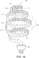
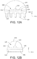
- FIGS. 1A and 1B illustrate embodiments wherein the support structure 111-a - 111-b is shaped into a spiral structure.
- the support structure may be a single, continuous element and in some cases, the support structure may comprise multiple discrete support elements.
- the support structure can be a solid shape that has holes cut or formed in it; the support structure can be a frame with spaces between the frame elements; the support structure can be a mesh, for example.
- a single continuous LED assembly having interconnected LEDs 121-a -- 121-1 may be disposed on a continuous or discrete element support structure. In some embodiments, multiple LED assemblies may be disposed on a continuous or discrete element support structure. In some embodiments, as shown in FIGS.
- the luminous volume (shape) defined by the surface 112-a, 112-b, 112-g, 112-h defined by the support structure 111-a, 111-b, 111-g, 111-h, 111-k, 111-1 may have a sphericity greater than about 0.5 or even greater than about 0.7.
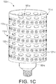
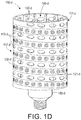
- the support structure may be cylindrical, as shown in FIGS. 1C - 1F .
- the openings 113-c, 113-d may be holes in the cylindrical support 111-c, 111-d.
- the support structure 111-e, 111-f may be a cylindrical frame and the openings 113-e, 113-f are spaces between the frame elements.
- the support structure 111-i, 111-j may define a conical shape.
- the support structure 111-k, 111-1 may be formed of a mesh.
- the LED assemblies 120-k, 120-1 may comprise micro LEDs.
- the support structure 111-a - 111-1 provides the shape and rigidity for the LED light bulb 100-a - 100-1 and can also impart thermal and/or optical characteristics to the LED light bulb 100-a - 100-1.
- the support structure may be made of metal, plastic, molded plastic, and/or a composite of several materials. In embodiments wherein the support structure is or includes a metal, the metal may be anodized, oxidized or otherwise coated with an appropriate coating material.
- the support structure comprises a cured structural coating.
- the cured structural coating may comprise a thermosetting material, a radiation cured material, e.g., a UV-cured material such as a UV cured polymer or UV - setting epoxy.
- the cured coating may comprise metal particles, such as mica, silver, gold and/or copper particles.
- the structural coating can be configured to dissipate heat generated by the LEDs.
- the cured structural coating may be disposed over at least a portion of the LEDs and configured to transmit the light generated by the LEDs.
- the cured coating forms a lens that directs light emitted by the LEDs.
- the cured structural coating can have a surface that is exposed to ambient air (inside or outside the open volume) that has a surface texture with an effective surface area at least three times greater than an untextured surface of the same size.
- the support structure 111-a - 111-1 can have a thermal conductivity greater than about 100 W/mK, greater than about 250 W/mK, or even greater than about 300 W/mK.
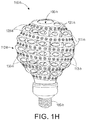
- the support structure 111-b, 111-d, 111-f, 111-h, 111-j, 111-1 may have cooling structures 130-b, 130-d, 130-f, 130-h, 130-j, 130-1, e.g., cooling fins, configured to dissipate the heat generated by the LEDs.
- the cooling structures can be disposed on the outside of the support structure (i.e., outside the open volume) as shown in FIGS. 1H and 1J and/or can be disposed on the inside of the support structure (i.e., inside the open volume) as illustrated in FIGS. 1B , 1D , 1F , 1L .
- At least one major surface of the support structure has a surface texture that provides a surface area at least three times greater than an untextured surface of the same size and shape. Texturing of the support structure surface can be used to impart certain optical and/or thermal properties to the support structure.
- the support structure has a reflectivity greater than 85% for visible light, e.g., wavelengths between about 320 nm and 700 nm.
- the support structure can comprise a material and/or have a surface texture that is configured to scatter light emitted by the LEDs 121-a - 121-l.
- each of the LEDs 121-a - 121-l can have a light emitting surface or edge that is substantially perpendicular to a major surface of the substrate. In some implementations, each of the LEDs 121-a - 121-1 can have a light emitting surface or edge that is substantially parallel to major surface of the substrate. According to some aspects, a first group of the LEDs can be electrically coupled to provide relatively lower light output and a second group of the LEDs electrically coupled to provide relatively higher light output.
- the substrate of an LED assembly comprises a flexible printed circuit board and the LEDS comprise surface mount LEDs.
- the LEDs 121-k, 121-1 comprise micro LEDs. Micro LEDs are many LEDs formed together in an integrated circuit, which may be flexible.
- one or more coatings may be disposed over at least a portion of the LED assemblies 120-a - 120-1.
- the coating has a surface that is exposed to ambient air, e.g., outside or inside the open volume 190-a - 190-1.
- the coating may comprise one or more of ceramic, glass, polymer, plastic, and metal powder.
- the coating can be configured to provide certain optical and/or thermal properties.
- coating surface has a surface texture that provides a surface area at least three times greater than an untextured surface of the same size.
- the coating can be configured to transmit and/or scatter the light generated by the LEDs.
- the coating may form a lens configured to direct the light emitted by the LEDs.
- the LED light bulb can additionally or alternatively include at least one thermally diffusive layer or coating disposed on the support structure.
- FIGS. 2A and 2B illustrate portions of LED assemblies that include a flexible substrate 210 and LEDs 220 spaced apart along the flexible substrate.
- the LEDs 220 are arranged on the substrate 210 in a single row.
- FIG. 2B illustrates another LED assembly formation in which there are two rows of LEDs 220 arranged on the flexible substrate 210.
- the LEDs may be arranged along the flexible substrate in any convenient pattern. The pattern may be selected to provide desired light distribution and/or heat dissipation specifications.
- the flexible substrate 210 may be a flexible circuit board that facilitates electrical connection between the LEDs 220 and the base electronics. As shown in FIGS. 2A and 2B , electrical conductors 230 are disposed in or on the flexible substrate and run along the length of the flexible substrate to electrically connect each of the LEDs 220 to the base electronics disposed within the base (shown in FIGS. 1A and 1B ).
- the LEDs 220 may comprise surface mount LEDs that are soldered to the flexible substrate or may be micro LEDs
- LEDs emit light from a surface or edge, as conceptually illustrated by arrows 350.
- one or more of the LEDs 320 may be arranged on the flexible substrate 310 so that the light emitting surface or edge 321 of the LED 320 is substantially parallel to a major surface 311 of the flexible substrate 310.
- one or more of the LEDs 330 may be arranged on the flexible substrate 310 so that the light emitting surface or edge 331 of the LED 330 is substantially perpendicular to a major surface 311 of the flexible substrate 310.
- LEDs 320, 330 may be arranged together on the flexible substrate 310 so that some of the LEDs 320 emit light 350 from a light emitting surface 321 that is about parallel with the major surface 311 of the flexible substrate 310 and some LEDs 330 emit light 350 from a light emitting surface 331 that is about perpendicular or at an angle to the major surface 311 as shown in FIG. 3C .
- the forming and attaching comprises forming the support structure into the predetermined shape after attaching the at least one LED assembly.
- Forming the support structure may comprise one or more of folding, bending, molding, and curing.
- the support structure is hardened to a rigid or semi-rigid condition by curing, the support structure is cured after being formed into the predetermined shape.
- the LED assembly is arranged lengthwise along the elongated support structure and can be attached thereto, e.g., by lamination, adhesion, or other suitable processes.
- the width of the LED assembly is equal to (or about equal to) the width of the support structure.
- the support structure is bent, folded, molded and/or cured into the shape of the light bulb.
- the support structure is mechanically attached to the base which holds the support structure upright, in many cases without need for additional support.
- the LEDs are electrically coupled to the base electronics.
- the flexible LED assembly can be mechanically wound in a spiral on a cylindrical form.
- the cylindrical form is cut, e.g., laser cut, or mechanically machined along the edges of the flexible substrate so that underlying form (with the LED assembly attached thereto) can be expanded to form the light bulb shape.
- the flexible LED assembly is then supported on the rigid or semi-rigid form, which has been spiral cut and expanded.
- Suitable materials for the support structure comprise materials that can be formed into the desired light bulb shape, such as metals, plastics, ceramics curable resins, and/or composite materials that include layers, portions, and/or mixtures of different materials. If metal is used for the support structure, the metal can be anodized, e.g., to enhance durability or the metal can be oxidized. In some embodiments, a surface of the support structure may be textured through embossing, etching, sandblasting, etc., to increase the effective surface area of the support structure surface. The surface texturing process can impart a significant increase in effective surface area.
- the texture of the surface of the support structure may have a surface roughness that provides an effective surface area that is at least equal to three times the surface area of the same material of the same size that does not have the texturing treatment.
- the surface texture may provide additional heat dissipation and/or may provide additional light diffusion or light scattering when compared with an untextured surface.
- the surface roughness (Ra) after texturing may be equal to at least 2 to 3 times that of an untextured surface of the same size.
- the support structure is configured to support the LED assembly as well as to provide heat dissipation and/or light management for the LED light bulb.
- the support structure is a heatsink.
- Thermally diffusive layers e.g. one or more layers of materials having thermal conductivity greater than about 100 W/mK, greater than about 250 W/mK, or even greater than about 300 W/mK can be applied to one or both surfaces and/or one or both edges of the support structure.
- the support structure (and/or a coating disposed thereon) may be used to diffuse, reflect, transmit, homogenize and/or blend the light emitted by the individual LEDs to provide a specified light spectral and/or intensity distribution.
- the support structure may have a reflective surface, may be coated with a reflective layer, may be textured to diffuse light or may otherwise be arranged to manage light emitted by the LEDs.
- the reflectivity of the surface or layer may be greater than about 85% at the wavelengths of light emitted by the LEDs, e.g., in a range of about 320 nm to about 700 nm.
- the transmissivity of the surface or layer may be greater than about 85% at the wavelengths of light emitted by the LEDs, e.g., in a range of about 320 nm to about 700 nm.
- the support structure surface may be configured to provide light scattering to the lighting device.
- the light scattering may be provided by a coating disposed on the support structure and/or the LED assembly.
- Suitable coatings may include, for example, reflective metals, glass, translucent plastics, etc.
- more than one type of coating is used to provide the lighting structure with various characteristics. For example, one coating may be selected to dissipate heat generated by the LEDs. Another coating may be selected to provide one or more optical characteristics. The coating may be applied to a surface of one or both of the support structure and the LED assemblies.
- the method includes arranging an optical sheet over a light emitting surface of the LEDs.
- an optical or thermal layer can be deposited on one or both of a major surface of the LED assemblies and a major surface of the structural support.
- the deposited layer can be optically or thermally diffusive. If an optical layer is deposited, the optical layer may comprise a material that provides one or more of light transmission, reflection and diffusion.
- FIGS. 5A-5G are perspective and cross section diagrams that illustrate various support structure/LED assembly configurations.
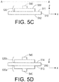
- the support structure is substantially flat as in the example illustrated in the perspective view of FIG. 5A .
- an LED assembly 520 comprising a flexible substrate 530 and LEDs 540 is coupled to one flat surface of the support structure 510.
- FIG. 5A illustrates the orientation of the LED assembly with respect to reference coordinates. The same orientation is used for diagrams that follow.
- the length of the flexible substrate 530 (along the y direction in FIG. 5A ) is much greater than its width (along the x direction in FIG. 5A ).
- FIG. 5C is a cross sectional diagram of the support structure/LED assembly configuration shown in FIG. 5A , where the cross section is taken along dashed line A - A'.
- the support structure may optionally include one or more textured surfaces 511, 512.
- FIG. 5D shows a flat support structure 512 with a first LED assembly 520a coupled to a first surface 513 of the support structure 510 and second LED assembly 520b coupled to a second surface 514 of the support structure that is opposite to the first surface.
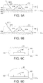
- the support structure may be a convex support structure 551 (shown in FIG. 5E ) or may be a concave support structure (shown in FIG. 5F).
- FIG. 5E illustrates an example in which the LED assembly 520 (comprising flexible substrate 530 and LEDs 540) is coupled to the convex surface of a support structure 551.
- FIG. 5F shows the LED assembly 520 coupled to a concave surface of a support structure 552.
- a triangular support structure 553 supports a first LED assembly 520a on a first facet 553a and a second LED assembly 520b on a second facet 553b. It will be appreciated that the examples provided herein are only a few of the many support structure/LED assembly configurations that are possible.
- the support structure may comprise metal, metal alloy, plastic or any other material suitable for forming into the desired LED light bulb shape.
- the support structure may be composite structure that includes multiple layers, multiple portions and/or multiple materials.
- the different layers, portions or materials of a composite support structure can impart different characteristics to the support structure.
- a layer, portion, and/or material may be used to impart structural characteristics
- a layer, portion, and/or material may be used to additionally impart structural and thermal characteristics
- a layer, portion, and/or material may be used to impart structural and optical characteristics.
- a composite support structure may comprise a layer or component that includes multiple materials, e.g., metal particles embedded in a plastic matrix.
- a composite support structure may comprise layers and/or portions made of different materials, as illustrated in FIG. 6 . Each of the layers and portions shown in FIG. 6 can contribute to the structural characteristics of the structural support.
- FIG. 6 illustrates a support structure/LED assembly combination where the support structure 610 is a composite of multiple layers 612, 613 and portions 611a, 611b.
- An LED assembly 620 (including a flexible substrate 630 and LEDs 640) is disposed on the support structure 610.
- the support structure includes a relatively thick, non-metallic, e.g., plastic, layer 613 that provides structural support, a relatively thin metallic layer 612 that contributes to the structural characteristics of the support 610 and also provides dissipation and/or distribution of heat generated by the LEDs 640.
- Reflective portions 611a, 611b e.g. plastic and/or metal reflectors
- the structural support may include surface texture that provides desired characteristics. Additionally or alternatively, the support structure may comprise features or portions that provide desired characteristics, such as the reflector portions 611a, 611b shown in FIG. 6.
- FIG. 7 shows another example of support structure with optional features.
- the support structure 710 includes heat sink fins 750 disposed on a surface of the support structure opposite to the surface on which the LED assembly 720 is arranged. The fins 750 may run along the width and/or length of the support structure 710 and may be designed to impart one or both of rigidity and heat removal capacity to the support structure.
- FIG. 8 illustrates several optional coatings that may be used.
- Portions of the LED assembly 820 and/or portions of the support structure 810 may be coated with an optical coating 850 that covers at least a portion of the flexible substrate 830 and/or some of the LEDs 840.
- the optical coating 850 may serve to diffuse or homogenize the light that emerges from the LEDs 840 so that the LED light bulb provides a light distribution that approaches or is comparable to that of an incandescent light of similar form factor and luminosity.
- the coating 850 may have a surface texture 851 that provides for heat dissipation and/or light diffusion. As previously discussed, the surface texture 851 can provide an effective surface area that could be greater than three times the surface area of an untextured surface of the same material and of the same size and shape.
- the configuration of FIG. 8 may include a thermally conductive layer 860 disposed on the support structure 810.
- the LED assembly is disposed along a first surface 811 of the support structure 810 and the thermally conductive layer 860 is disposed on an opposing second surface 812 of the support structure 810.
- a thermally conductive layer may be disposed on the same surface as the LED assembly or a thermally conductive layer may be disposed on both surfaces of the support structure.
- the configuration shown in FIG. 8 includes a phosphor layer 870 disposed on the first surface 811 of the structural support 810.
- the phosphor layer comprises a fluorescent material that may emit light at a different wavelength than the light emitted by the LEDS.
- the light emitted by the LED and the phosphor layer may provide a broader spectral characteristic for the light that emerges from the LED light bulb.
- the LEDs may emit blue light and a yellow phosphor may be coated on the structural support and/or embedded in the coating 850.
- an optical coating and/or sheet may be disposed over the LEDs as a waveguide to guide the light for a distance along the LED assembly until the light is coupled out of the waveguide.
- FIG. 9A shows a structural support 910 having a LED assembly 920 disposed thereon.
- a coating 950 is disposed over the LEDs 940.
- the difference in the index of refraction of the coating 950 and air at the optical coating/air interface 952 provides total internal reflection (TIR) at the interface 952 for at least some of the light emitted by the LEDs 940.
- FIG. 9A illustrates light beam 950 that emerges from LED 940a and is guided between the coating surface 951 and the flexible substrate 930 for a distance.
- Arrow 951a represents light that emerges from LED 940a.
- the light is reflected along arrow 951b at the interface 952.
- the light is reflected again at the surface of the flexible substrate 930 (which may include reflective coating 921) along arrow 951c.
- FIG. 9B is similar in many respects to FIG. 9C.
- FIG. 9B illustrates an optical sheet that may overlie the LEDs to facilitate guiding or waveguiding the light emitted by the LEDs.
- the interface between the optical sheet and air or between the optical sheet and the coating provide a TIR interface for the emitted light.
- an optical coating and/or optical sheet may form or comprise a light directing surface with various surface features 970, 980 such as linear prisms 970 and/or lenses or lenticular structures 980 that direct the light emitted from the LEDs.
- the LED assembly is formed into a predetermined shape and a curable coating is disposed over at least a portion of the LED assembly. After curing, the cured structural coating is used to maintain the LED assembly in the predetermined shape.
- FIG. 10 is a flow diagram that describes a process of forming an LED light bulb in accordance with some embodiments.
- An LED assembly comprising a flexible substrate with LEDs disposed thereon is formed 1010 into a predetermined shape.
- the LED assembly may be placed in the shape of a spiral that is similar in size and overall shape to an incandescent light bulb of equivalent luminosity.
- a curable coating that can be hardened into a rigid or semi-rigid support is applied 1020 to the LED assembly, e.g., by various coating processes or by overmolding.
- the curable coating may contain or be a cureable polymer, a curable plastic, or a cureable composite.
- a curable composite can include a resin that includes particles in a curable polymer matrix. The particles may provide or enhance various optical or thermal properties of the cured structural coating. For example, metal particles embedded in a curable polymer matrix may provide increased heat dissipation for the heat generated by the LEDs. Optical particles embedded in the matrix may increase light scattering (and/or other optical properties).
- the curable coating may comprise a coating that is curable by thermosetting, radiation exposure (such as UV radiation), electron beam exposure, and/or other types of curable coating.
- the cureable coating Prior to coating, the cureable coating has viscosity suitable for coating or overmolding the LED assembly.
- the curable coating may be applied by any suitable process, for example, by overmolding, dip coating, spray coating and/or slit die coating.
- the curable coating bonds or adheres to the flexible substrate.
- the curable coating is cured 1030, and after curing, the cured structural coating serves as a rigid or semi-rigid support that maintains the LED assembly in the predetermined shape.
- the coating can be cured by any appropriate process depending on the material used for the coating. For example, curing may involve thermosetting, heating, cooling, applying pressure, chemicals, radiation, e.g., ultraviolet radiation, electron beam, and/or other curing processes.
- the light produced by the LEDs on the LED assembly is used to cure the coating and thus set the shape of the LED light bulb.
- the curable coating may be cured by cooling the coating so that is solidifies on, over, or around the LED assembly.
- the LED assembly may be coated before it is placed in the predetermined shape. After coating, the LED assembly is placed in the predetermined shape and the curable coating is subsequently cured. In some approaches, the LED assembly is placed in the predetermined shape first, after which the LED assembly is coated with the cureable coating.
- the cured structural coating may partially or fully cover the LED assembly.
- the structural coating can provide thermal and/or light management for the LED light bulb.
- the structural coating can dissipate heat generated by the LEDs.
- the structural coating can provide various optical properties.
- the structural coating can be an optical reflector, an optical diffuser, a scattering medium, and/or a waveguiding medium for controlling light output.
- the structural coating can be used in conjunction with additional coatings or layers.
Landscapes
- Engineering & Computer Science (AREA)
- Microelectronics & Electronic Packaging (AREA)
- General Engineering & Computer Science (AREA)
- Manufacturing & Machinery (AREA)
- Computer Hardware Design (AREA)
- Power Engineering (AREA)
- Physics & Mathematics (AREA)
- Optics & Photonics (AREA)
- Non-Portable Lighting Devices Or Systems Thereof (AREA)
- Arrangement Of Elements, Cooling, Sealing, Or The Like Of Lighting Devices (AREA)
- Fastening Of Light Sources Or Lamp Holders (AREA)
- Led Device Packages (AREA)
Applications Claiming Priority (1)
| Application Number | Priority Date | Filing Date | Title |
|---|---|---|---|
| US13/802,343 US9528689B2 (en) | 2013-03-13 | 2013-03-13 | LED lighting device with cured structural support |
Publications (3)
| Publication Number | Publication Date |
|---|---|
| EP2778503A2 EP2778503A2 (en) | 2014-09-17 |
| EP2778503A3 EP2778503A3 (en) | 2015-09-02 |
| EP2778503B1 true EP2778503B1 (en) | 2019-05-08 |
Family
ID=50396855
Family Applications (1)
| Application Number | Title | Priority Date | Filing Date |
|---|---|---|---|
| EP14158755.0A Active EP2778503B1 (en) | 2013-03-13 | 2014-03-11 | LED lighting device with cured structural support |
Country Status (4)
| Country | Link |
|---|---|
| US (2) | US9528689B2 (zh) |
| EP (1) | EP2778503B1 (zh) |
| JP (1) | JP6158728B2 (zh) |
| CN (1) | CN104048196B (zh) |
Families Citing this family (33)
| Publication number | Priority date | Publication date | Assignee | Title |
|---|---|---|---|---|
| US9995474B2 (en) * | 2015-06-10 | 2018-06-12 | Jiaxing Super Lighting Electric Appliance Co., Ltd. | LED filament, LED filament assembly and LED bulb |
| US9353932B2 (en) * | 2013-03-13 | 2016-05-31 | Palo Alto Research Center Incorporated | LED light bulb with structural support |
| US9528689B2 (en) | 2013-03-13 | 2016-12-27 | Palo Alto Research Center Incorporated | LED lighting device with cured structural support |
| US10711962B2 (en) | 2014-09-24 | 2020-07-14 | Anglers-Friend, Llc | Spiral wrap power and lighting system |
| US10317022B2 (en) * | 2014-09-24 | 2019-06-11 | Angler's-Friend, LLC | Spiral wrap lighting system |
| HK1207250A2 (zh) * | 2014-10-15 | 2016-01-22 | 新照明設計有限公司 號 | 封裝用基板、立體 封裝、具有該立體 封裝的燈泡及其製作方法 |
| WO2015171014A1 (ru) * | 2014-12-26 | 2015-11-12 | Юрий Борисович СОКОЛОВ | Светодиодная лампа общего назначения с литым корпусом-радиатором |
| US9523494B2 (en) * | 2015-02-17 | 2016-12-20 | Flextronics Ap, Llc | LED lighting unit |
| EP4023190B1 (en) | 2015-02-27 | 2024-04-03 | Colgate-Palmolive Company | Oral treatment system |
| CN106468402A (zh) * | 2015-08-07 | 2017-03-01 | 深圳市裕富照明有限公司 | Smt工艺的充气led灯泡 |
| CN108027121A (zh) * | 2015-09-04 | 2018-05-11 | 飞利浦照明控股有限公司 | 具有围绕支撑件缠绕的柔性电路条的照明设备 |
| ES2627558B1 (es) * | 2016-01-19 | 2018-06-14 | Microplus World Corporation, S.L. | Dispositivo emisor de luz para luminarias con microled de alta eficiencia. |
| CN106468423A (zh) * | 2016-02-03 | 2017-03-01 | 长荣科技发展(北京)有限公司 | 一种led投光灯 |
| CN109076693B (zh) | 2016-04-26 | 2021-09-03 | 昕诺飞控股有限公司 | 柔性固态照明带 |
| US10627099B2 (en) * | 2016-06-28 | 2020-04-21 | Signify Holding B.V. | Lighting assembly for emitting high intensity light, a light source, a lamp and a luminaire |
| CN106151904A (zh) * | 2016-08-24 | 2016-11-23 | 胡溢文 | 一种可卷绕灯丝的led灯及其制备工艺 |
| US10883694B2 (en) * | 2016-11-14 | 2021-01-05 | Lumileds Llc | Method of manufacturing an LED lighting assembly |
| TWI607677B (zh) * | 2016-11-21 | 2017-12-01 | 同泰電子科技股份有限公司 | 可撓性線路板結構 |
| AU2018297187B2 (en) | 2017-07-06 | 2023-07-13 | Schumacher Electric Corp. | Flashlight |
| US11530783B2 (en) * | 2017-11-20 | 2022-12-20 | Seoul Semiconductor Co., Ltd. | Bulb-type light source |
| KR102459144B1 (ko) * | 2017-11-20 | 2022-10-27 | 서울반도체 주식회사 | 전구형 광원 |
| US10129984B1 (en) * | 2018-02-07 | 2018-11-13 | Lockheed Martin Corporation | Three-dimensional electronics distribution by geodesic faceting |
| US11482568B2 (en) | 2018-06-28 | 2022-10-25 | Lumens Co., Ltd. | Flexible lighiing device and display panel using micro LED chips |
| CN113330245B (zh) * | 2019-01-24 | 2024-06-21 | 昕诺飞控股有限公司 | Led灯丝装置 |
| US10767816B1 (en) * | 2019-04-24 | 2020-09-08 | Xiamen Eco Lighting Co. Ltd. | Light bulb apparatus |
| EP4031803B1 (en) * | 2019-09-19 | 2023-11-08 | Signify Holding B.V. | Light-emitting diode filament arrangement comprising at least one bending unit |
| TWI687624B (zh) * | 2019-10-25 | 2020-03-11 | 液光固態照明股份有限公司 | 照明裝置 |
| WO2021094124A1 (en) * | 2019-11-11 | 2021-05-20 | Signify Holding B.V. | An led filament lamp and a method of producing a spiral led filament |
| CN114729728A (zh) * | 2019-11-21 | 2022-07-08 | 昕诺飞控股有限公司 | 发光设备 |
| KR20220113971A (ko) * | 2020-01-20 | 2022-08-17 | 레이아 인코포레이티드 | 광 배제 영역을 제공하는 미세슬릿 산란 소자 기반 백라이트, 멀티뷰 디스플레이 및 방법 |
| WO2022078813A1 (en) * | 2020-10-15 | 2022-04-21 | Signify Holding B.V. | A lighting device and a method of manufacturing a lighting device |
| US20240019092A1 (en) * | 2020-11-10 | 2024-01-18 | Signify Holding B.V. | A led light unit |
| EP4274994B1 (en) | 2021-01-05 | 2024-06-19 | Signify Holding B.V. | Led filament arrangement |
Citations (6)
| Publication number | Priority date | Publication date | Assignee | Title |
|---|---|---|---|---|
| CA2142132A1 (en) * | 1994-03-03 | 1995-09-04 | James C. Johnson | Methods and apparatus for illumination of signs utilizing light emitting diodes |
| US6580228B1 (en) * | 2000-08-22 | 2003-06-17 | Light Sciences Corporation | Flexible substrate mounted solid-state light sources for use in line current lamp sockets |
| US20110050073A1 (en) * | 2009-09-02 | 2011-03-03 | Liquidleds Lighting Corp. | Bending led bulb |
| US20110260945A1 (en) * | 2007-08-03 | 2011-10-27 | Fumio Karasawa | Coating Composition and Article Using the Same |
| US20110267812A1 (en) * | 2010-02-12 | 2011-11-03 | Cree, Inc. | Solid state lighting device, and method of assembling the same |
| US20120243212A1 (en) * | 2011-03-22 | 2012-09-27 | David Smith | Portable and bendable utility light |
Family Cites Families (35)
| Publication number | Priority date | Publication date | Assignee | Title |
|---|---|---|---|---|
| US6578986B2 (en) | 2001-06-29 | 2003-06-17 | Permlight Products, Inc. | Modular mounting arrangement and method for light emitting diodes |
| US6774566B2 (en) | 2001-09-19 | 2004-08-10 | Toshiba Lighting & Technology Corporation | High pressure discharge lamp and luminaire |
| EP2298229A1 (en) * | 2002-07-25 | 2011-03-23 | Jonathan S. Dahm | Method and apparatus for using light emitting diodes for curing |
| JP2004071342A (ja) * | 2002-08-06 | 2004-03-04 | Rosso:Kk | 照明装置 |
| JP2004253328A (ja) * | 2003-02-21 | 2004-09-09 | Moriyama Sangyo Kk | 発光装置及びledモジュール |
| US7086756B2 (en) * | 2004-03-18 | 2006-08-08 | Lighting Science Group Corporation | Lighting element using electronically activated light emitting elements and method of making same |
| US7585096B2 (en) | 2005-05-18 | 2009-09-08 | Visteon Global Technologies, Inc. | Compound trough reflector for LED light sources |
| CN100448331C (zh) * | 2007-04-30 | 2008-12-31 | 林万炯 | 柔性条形防水led灯成型工艺 |
| KR101110865B1 (ko) * | 2007-11-27 | 2012-02-15 | 엘이디라이텍(주) | 램프유닛 |
| US20090140279A1 (en) | 2007-12-03 | 2009-06-04 | Goldeneye, Inc. | Substrate-free light emitting diode chip |
| US7923272B2 (en) * | 2007-12-28 | 2011-04-12 | Hwang-Pao Lee | Method of forming a resin cover lens of LED assembly |
| GB0801509D0 (en) * | 2008-01-28 | 2008-03-05 | Photonstar Led Ltd | Light emitting system with optically transparent thermally conductive element |
| KR100978208B1 (ko) * | 2008-03-10 | 2010-08-25 | 민병현 | 조립형 엘이디 조명기기 |
| JP5198165B2 (ja) * | 2008-06-24 | 2013-05-15 | 出光興産株式会社 | 照明装置用の筐体およびこれを備えた照明装置 |
| KR100883344B1 (ko) | 2008-08-08 | 2009-02-12 | 김현민 | Led 조명램프 |
| KR101324077B1 (ko) * | 2008-08-26 | 2013-10-31 | 딩구오 판 | 발광 다이오드 멀티 칩 실장 및 실장 탑재로 만들어진 스트립 라이트 |
| US7998797B2 (en) * | 2008-12-09 | 2011-08-16 | Infineon Technologies Ag | Semiconductor device |
| JP5275785B2 (ja) * | 2008-12-25 | 2013-08-28 | アァルピィ東プラ株式会社 | Led照明器具及びその製造方法 |
| DE102009009288A1 (de) * | 2009-02-17 | 2010-08-26 | Osram Gesellschaft mit beschränkter Haftung | Starrflexible Trägerplatte |
| JP2010218714A (ja) | 2009-03-13 | 2010-09-30 | Makoto Ishihara | 螺旋状led発光体およびそれを用いたled照明器具 |
| CN201416866Y (zh) * | 2009-04-28 | 2010-03-03 | 林保龙 | 用于发光二极管的板型散热结构 |
| WO2011088190A2 (en) | 2010-01-15 | 2011-07-21 | Edward Lawrence Sinofsky | Lightweight solid state lighting panel |
| US8262249B2 (en) * | 2010-01-19 | 2012-09-11 | Lightel Technologies Inc. | Linear solid-state lighting with broad viewing angle |
| US8783915B2 (en) * | 2010-02-11 | 2014-07-22 | Bridgelux, Inc. | Surface-textured encapsulations for use with light emitting diodes |
| FR2957723A1 (fr) * | 2010-03-16 | 2011-09-23 | Design4 | Systeme pour l'alimentation electrique d'un dispositif d'eclairage a diodes electroluminescentes, dispositif d'eclairage a diodes electroluminescentes |
| JP5284308B2 (ja) * | 2010-04-19 | 2013-09-11 | 日本メクトロン株式会社 | フレキシブル回路基板及びその製造方法 |
| JP2011249536A (ja) * | 2010-05-26 | 2011-12-08 | Daisho Denshi Co Ltd | 折り曲げ可能配線基板、発光モジュール、発光モジュールの製造方法、折り曲げ可能配線基板の製造方法 |
| JP5486431B2 (ja) * | 2010-07-27 | 2014-05-07 | 日東電工株式会社 | 発光装置用部品、発光装置およびその製造方法 |
| PL2655956T3 (pl) * | 2010-12-22 | 2020-12-28 | Signify Holding B.V. | Urządzenie oświetleniowe i sposób wytwarzania urządzenia oświetleniowego |
| US8314566B2 (en) | 2011-02-22 | 2012-11-20 | Quarkstar Llc | Solid state lamp using light emitting strips |
| JP2013016493A (ja) * | 2011-07-05 | 2013-01-24 | Industrial Technology Research Inst | 照明装置およびその組み立て方法 |
| CN202419298U (zh) * | 2012-01-10 | 2012-09-05 | 深圳市科利尔照明科技有限公司 | 一种led灯带 |
| US9353932B2 (en) | 2013-03-13 | 2016-05-31 | Palo Alto Research Center Incorporated | LED light bulb with structural support |
| US9528689B2 (en) | 2013-03-13 | 2016-12-27 | Palo Alto Research Center Incorporated | LED lighting device with cured structural support |
| CN203363808U (zh) * | 2013-07-31 | 2013-12-25 | 温岭翊洲农业科技有限公司 | 一种新型led灯 |
-
2013
- 2013-03-13 US US13/802,343 patent/US9528689B2/en active Active
-
2014
- 2014-02-27 JP JP2014037166A patent/JP6158728B2/ja not_active Expired - Fee Related
- 2014-02-28 CN CN201410073313.XA patent/CN104048196B/zh not_active Expired - Fee Related
- 2014-03-11 EP EP14158755.0A patent/EP2778503B1/en active Active
-
2016
- 2016-12-12 US US15/375,752 patent/US9857031B2/en not_active Expired - Fee Related
Patent Citations (6)
| Publication number | Priority date | Publication date | Assignee | Title |
|---|---|---|---|---|
| CA2142132A1 (en) * | 1994-03-03 | 1995-09-04 | James C. Johnson | Methods and apparatus for illumination of signs utilizing light emitting diodes |
| US6580228B1 (en) * | 2000-08-22 | 2003-06-17 | Light Sciences Corporation | Flexible substrate mounted solid-state light sources for use in line current lamp sockets |
| US20110260945A1 (en) * | 2007-08-03 | 2011-10-27 | Fumio Karasawa | Coating Composition and Article Using the Same |
| US20110050073A1 (en) * | 2009-09-02 | 2011-03-03 | Liquidleds Lighting Corp. | Bending led bulb |
| US20110267812A1 (en) * | 2010-02-12 | 2011-11-03 | Cree, Inc. | Solid state lighting device, and method of assembling the same |
| US20120243212A1 (en) * | 2011-03-22 | 2012-09-27 | David Smith | Portable and bendable utility light |
Also Published As
| Publication number | Publication date |
|---|---|
| CN104048196A (zh) | 2014-09-17 |
| US20140268740A1 (en) | 2014-09-18 |
| CN104048196B (zh) | 2019-01-25 |
| US20170089519A1 (en) | 2017-03-30 |
| EP2778503A3 (en) | 2015-09-02 |
| EP2778503A2 (en) | 2014-09-17 |
| JP6158728B2 (ja) | 2017-07-05 |
| US9528689B2 (en) | 2016-12-27 |
| US9857031B2 (en) | 2018-01-02 |
| JP2014179319A (ja) | 2014-09-25 |
Similar Documents
| Publication | Publication Date | Title |
|---|---|---|
| EP2778503B1 (en) | LED lighting device with cured structural support | |
| EP2778502B1 (en) | LED light bulb with structural support | |
| US10989861B2 (en) | Edgelit LED blade fixture | |
| TWI553271B (zh) | 具有光導及整合之熱導的固態燈 | |
| US9091420B2 (en) | Illumination apparatus | |
| US7637628B2 (en) | LED light pod with modular optics and heat dissipation structure | |
| US20060146531A1 (en) | Linear lighting apparatus with improved heat dissipation | |
| US9267674B2 (en) | Solid state light with enclosed light guide and integrated thermal guide | |
| KR20130114142A (ko) | 경량의 히트 싱크들 및 이를 구비한 발광 다이오드 램프들 | |
| US20150055340A1 (en) | Optical array for led bulb with thermal optical diffuser | |
| US20120250297A1 (en) | Light Assembly | |
| CN107850272B (zh) | 具有光导的照明设备 |
Legal Events
| Date | Code | Title | Description |
|---|---|---|---|
| 17P | Request for examination filed |
Effective date: 20140311 |
|
| AK | Designated contracting states |
Kind code of ref document: A2 Designated state(s): AL AT BE BG CH CY CZ DE DK EE ES FI FR GB GR HR HU IE IS IT LI LT LU LV MC MK MT NL NO PL PT RO RS SE SI SK SM TR |
|
| AX | Request for extension of the european patent |
Extension state: BA ME |
|
| PUAI | Public reference made under article 153(3) epc to a published international application that has entered the european phase |
Free format text: ORIGINAL CODE: 0009012 |
|
| PUAL | Search report despatched |
Free format text: ORIGINAL CODE: 0009013 |
|
| AK | Designated contracting states |
Kind code of ref document: A3 Designated state(s): AL AT BE BG CH CY CZ DE DK EE ES FI FR GB GR HR HU IE IS IT LI LT LU LV MC MK MT NL NO PL PT RO RS SE SI SK SM TR |
|
| AX | Request for extension of the european patent |
Extension state: BA ME |
|
| RIC1 | Information provided on ipc code assigned before grant |
Ipc: H05K 1/18 20060101ALI20150728BHEP Ipc: H05K 1/02 20060101ALN20150728BHEP Ipc: F21Y 101/02 20060101ALN20150728BHEP Ipc: F21Y 111/00 20060101ALN20150728BHEP Ipc: H01L 33/54 20100101ALI20150728BHEP Ipc: H01L 33/52 20100101ALI20150728BHEP Ipc: H05K 3/28 20060101ALN20150728BHEP Ipc: F21K 99/00 20100101AFI20150728BHEP |
|
| R17P | Request for examination filed (corrected) |
Effective date: 20160302 |
|
| RBV | Designated contracting states (corrected) |
Designated state(s): AL AT BE BG CH CY CZ DE DK EE ES FI FR GB GR HR HU IE IS IT LI LT LU LV MC MK MT NL NO PL PT RO RS SE SI SK SM TR |
|
| STAA | Information on the status of an ep patent application or granted ep patent |
Free format text: STATUS: EXAMINATION IS IN PROGRESS |
|
| 17Q | First examination report despatched |
Effective date: 20161207 |
|
| REG | Reference to a national code |
Ref country code: DE Ref legal event code: R079 Ref document number: 602014046105 Country of ref document: DE Free format text: PREVIOUS MAIN CLASS: F21K0099000000 Ipc: F21K0009232000 |
|
| GRAP | Despatch of communication of intention to grant a patent |
Free format text: ORIGINAL CODE: EPIDOSNIGR1 |
|
| STAA | Information on the status of an ep patent application or granted ep patent |
Free format text: STATUS: GRANT OF PATENT IS INTENDED |
|
| RIC1 | Information provided on ipc code assigned before grant |
Ipc: F21K 9/232 20140917AFI20181105BHEP Ipc: H05K 1/02 20060101ALI20181105BHEP Ipc: F21Y 107/00 20140917ALN20181105BHEP Ipc: H05K 1/18 20060101ALN20181105BHEP Ipc: F21Y 115/10 20140917ALN20181105BHEP Ipc: H01L 33/54 20100101ALI20181105BHEP Ipc: F21Y 111/00 20060101ALN20181105BHEP Ipc: H05K 3/28 20060101ALN20181105BHEP |
|
| INTG | Intention to grant announced |
Effective date: 20181206 |
|
| RIC1 | Information provided on ipc code assigned before grant |
Ipc: F21Y 115/10 20160101ALN20181105BHEP Ipc: F21Y 111/00 20160101ALN20181105BHEP Ipc: H05K 1/02 20060101ALI20181105BHEP Ipc: H05K 1/18 20060101ALN20181105BHEP Ipc: F21K 9/232 20160101AFI20181105BHEP Ipc: H05K 3/28 20060101ALN20181105BHEP Ipc: F21Y 107/00 20160101ALN20181105BHEP Ipc: H01L 33/54 20100101ALI20181105BHEP |
|
| RIC1 | Information provided on ipc code assigned before grant |
Ipc: F21Y 115/10 20160101ALN20181105BHEP Ipc: H01L 33/54 20100101ALI20181105BHEP Ipc: H05K 1/02 20060101ALI20181105BHEP Ipc: F21K 9/232 20160101AFI20181105BHEP Ipc: H05K 1/18 20060101ALN20181105BHEP Ipc: H05K 3/28 20060101ALN20181105BHEP Ipc: F21Y 111/00 20160101ALN20181105BHEP Ipc: F21Y 107/00 20160101ALN20181105BHEP |
|
| GRAS | Grant fee paid |
Free format text: ORIGINAL CODE: EPIDOSNIGR3 |
|
| GRAA | (expected) grant |
Free format text: ORIGINAL CODE: 0009210 |
|
| STAA | Information on the status of an ep patent application or granted ep patent |
Free format text: STATUS: THE PATENT HAS BEEN GRANTED |
|
| AK | Designated contracting states |
Kind code of ref document: B1 Designated state(s): AL AT BE BG CH CY CZ DE DK EE ES FI FR GB GR HR HU IE IS IT LI LT LU LV MC MK MT NL NO PL PT RO RS SE SI SK SM TR |
|
| REG | Reference to a national code |
Ref country code: GB Ref legal event code: FG4D |
|
| REG | Reference to a national code |
Ref country code: CH Ref legal event code: EP Ref country code: AT Ref legal event code: REF Ref document number: 1130685 Country of ref document: AT Kind code of ref document: T Effective date: 20190515 |
|
| REG | Reference to a national code |
Ref country code: IE Ref legal event code: FG4D |
|
| REG | Reference to a national code |
Ref country code: DE Ref legal event code: R096 Ref document number: 602014046105 Country of ref document: DE |
|
| REG | Reference to a national code |
Ref country code: NL Ref legal event code: MP Effective date: 20190508 |
|
| REG | Reference to a national code |
Ref country code: LT Ref legal event code: MG4D |
|
| PG25 | Lapsed in a contracting state [announced via postgrant information from national office to epo] |
Ref country code: LT Free format text: LAPSE BECAUSE OF FAILURE TO SUBMIT A TRANSLATION OF THE DESCRIPTION OR TO PAY THE FEE WITHIN THE PRESCRIBED TIME-LIMIT Effective date: 20190508 Ref country code: HR Free format text: LAPSE BECAUSE OF FAILURE TO SUBMIT A TRANSLATION OF THE DESCRIPTION OR TO PAY THE FEE WITHIN THE PRESCRIBED TIME-LIMIT Effective date: 20190508 Ref country code: NL Free format text: LAPSE BECAUSE OF FAILURE TO SUBMIT A TRANSLATION OF THE DESCRIPTION OR TO PAY THE FEE WITHIN THE PRESCRIBED TIME-LIMIT Effective date: 20190508 Ref country code: ES Free format text: LAPSE BECAUSE OF FAILURE TO SUBMIT A TRANSLATION OF THE DESCRIPTION OR TO PAY THE FEE WITHIN THE PRESCRIBED TIME-LIMIT Effective date: 20190508 Ref country code: SE Free format text: LAPSE BECAUSE OF FAILURE TO SUBMIT A TRANSLATION OF THE DESCRIPTION OR TO PAY THE FEE WITHIN THE PRESCRIBED TIME-LIMIT Effective date: 20190508 Ref country code: FI Free format text: LAPSE BECAUSE OF FAILURE TO SUBMIT A TRANSLATION OF THE DESCRIPTION OR TO PAY THE FEE WITHIN THE PRESCRIBED TIME-LIMIT Effective date: 20190508 Ref country code: NO Free format text: LAPSE BECAUSE OF FAILURE TO SUBMIT A TRANSLATION OF THE DESCRIPTION OR TO PAY THE FEE WITHIN THE PRESCRIBED TIME-LIMIT Effective date: 20190808 Ref country code: PT Free format text: LAPSE BECAUSE OF FAILURE TO SUBMIT A TRANSLATION OF THE DESCRIPTION OR TO PAY THE FEE WITHIN THE PRESCRIBED TIME-LIMIT Effective date: 20190908 Ref country code: AL Free format text: LAPSE BECAUSE OF FAILURE TO SUBMIT A TRANSLATION OF THE DESCRIPTION OR TO PAY THE FEE WITHIN THE PRESCRIBED TIME-LIMIT Effective date: 20190508 |
|
| PG25 | Lapsed in a contracting state [announced via postgrant information from national office to epo] |
Ref country code: GR Free format text: LAPSE BECAUSE OF FAILURE TO SUBMIT A TRANSLATION OF THE DESCRIPTION OR TO PAY THE FEE WITHIN THE PRESCRIBED TIME-LIMIT Effective date: 20190809 Ref country code: LV Free format text: LAPSE BECAUSE OF FAILURE TO SUBMIT A TRANSLATION OF THE DESCRIPTION OR TO PAY THE FEE WITHIN THE PRESCRIBED TIME-LIMIT Effective date: 20190508 Ref country code: RS Free format text: LAPSE BECAUSE OF FAILURE TO SUBMIT A TRANSLATION OF THE DESCRIPTION OR TO PAY THE FEE WITHIN THE PRESCRIBED TIME-LIMIT Effective date: 20190508 Ref country code: BG Free format text: LAPSE BECAUSE OF FAILURE TO SUBMIT A TRANSLATION OF THE DESCRIPTION OR TO PAY THE FEE WITHIN THE PRESCRIBED TIME-LIMIT Effective date: 20190808 |
|
| REG | Reference to a national code |
Ref country code: AT Ref legal event code: MK05 Ref document number: 1130685 Country of ref document: AT Kind code of ref document: T Effective date: 20190508 |
|
| PG25 | Lapsed in a contracting state [announced via postgrant information from national office to epo] |
Ref country code: RO Free format text: LAPSE BECAUSE OF FAILURE TO SUBMIT A TRANSLATION OF THE DESCRIPTION OR TO PAY THE FEE WITHIN THE PRESCRIBED TIME-LIMIT Effective date: 20190508 Ref country code: SK Free format text: LAPSE BECAUSE OF FAILURE TO SUBMIT A TRANSLATION OF THE DESCRIPTION OR TO PAY THE FEE WITHIN THE PRESCRIBED TIME-LIMIT Effective date: 20190508 Ref country code: CZ Free format text: LAPSE BECAUSE OF FAILURE TO SUBMIT A TRANSLATION OF THE DESCRIPTION OR TO PAY THE FEE WITHIN THE PRESCRIBED TIME-LIMIT Effective date: 20190508 Ref country code: AT Free format text: LAPSE BECAUSE OF FAILURE TO SUBMIT A TRANSLATION OF THE DESCRIPTION OR TO PAY THE FEE WITHIN THE PRESCRIBED TIME-LIMIT Effective date: 20190508 Ref country code: EE Free format text: LAPSE BECAUSE OF FAILURE TO SUBMIT A TRANSLATION OF THE DESCRIPTION OR TO PAY THE FEE WITHIN THE PRESCRIBED TIME-LIMIT Effective date: 20190508 Ref country code: DK Free format text: LAPSE BECAUSE OF FAILURE TO SUBMIT A TRANSLATION OF THE DESCRIPTION OR TO PAY THE FEE WITHIN THE PRESCRIBED TIME-LIMIT Effective date: 20190508 |
|
| REG | Reference to a national code |
Ref country code: DE Ref legal event code: R097 Ref document number: 602014046105 Country of ref document: DE |
|
| PG25 | Lapsed in a contracting state [announced via postgrant information from national office to epo] |
Ref country code: IT Free format text: LAPSE BECAUSE OF FAILURE TO SUBMIT A TRANSLATION OF THE DESCRIPTION OR TO PAY THE FEE WITHIN THE PRESCRIBED TIME-LIMIT Effective date: 20190508 Ref country code: SM Free format text: LAPSE BECAUSE OF FAILURE TO SUBMIT A TRANSLATION OF THE DESCRIPTION OR TO PAY THE FEE WITHIN THE PRESCRIBED TIME-LIMIT Effective date: 20190508 |
|
| PLBE | No opposition filed within time limit |
Free format text: ORIGINAL CODE: 0009261 |
|
| STAA | Information on the status of an ep patent application or granted ep patent |
Free format text: STATUS: NO OPPOSITION FILED WITHIN TIME LIMIT |
|
| PG25 | Lapsed in a contracting state [announced via postgrant information from national office to epo] |
Ref country code: TR Free format text: LAPSE BECAUSE OF FAILURE TO SUBMIT A TRANSLATION OF THE DESCRIPTION OR TO PAY THE FEE WITHIN THE PRESCRIBED TIME-LIMIT Effective date: 20190508 |
|
| 26N | No opposition filed |
Effective date: 20200211 |
|
| PG25 | Lapsed in a contracting state [announced via postgrant information from national office to epo] |
Ref country code: PL Free format text: LAPSE BECAUSE OF FAILURE TO SUBMIT A TRANSLATION OF THE DESCRIPTION OR TO PAY THE FEE WITHIN THE PRESCRIBED TIME-LIMIT Effective date: 20190508 |
|
| PGFP | Annual fee paid to national office [announced via postgrant information from national office to epo] |
Ref country code: GB Payment date: 20200221 Year of fee payment: 7 |
|
| PG25 | Lapsed in a contracting state [announced via postgrant information from national office to epo] |
Ref country code: SI Free format text: LAPSE BECAUSE OF FAILURE TO SUBMIT A TRANSLATION OF THE DESCRIPTION OR TO PAY THE FEE WITHIN THE PRESCRIBED TIME-LIMIT Effective date: 20190508 |
|
| PGFP | Annual fee paid to national office [announced via postgrant information from national office to epo] |
Ref country code: FR Payment date: 20200220 Year of fee payment: 7 |
|
| PG25 | Lapsed in a contracting state [announced via postgrant information from national office to epo] |
Ref country code: MC Free format text: LAPSE BECAUSE OF FAILURE TO SUBMIT A TRANSLATION OF THE DESCRIPTION OR TO PAY THE FEE WITHIN THE PRESCRIBED TIME-LIMIT Effective date: 20190508 |
|
| REG | Reference to a national code |
Ref country code: CH Ref legal event code: PL |
|
| REG | Reference to a national code |
Ref country code: BE Ref legal event code: MM Effective date: 20200331 |
|
| PG25 | Lapsed in a contracting state [announced via postgrant information from national office to epo] |
Ref country code: LU Free format text: LAPSE BECAUSE OF NON-PAYMENT OF DUE FEES Effective date: 20200311 |
|
| PG25 | Lapsed in a contracting state [announced via postgrant information from national office to epo] |
Ref country code: IE Free format text: LAPSE BECAUSE OF NON-PAYMENT OF DUE FEES Effective date: 20200311 Ref country code: CH Free format text: LAPSE BECAUSE OF NON-PAYMENT OF DUE FEES Effective date: 20200331 Ref country code: LI Free format text: LAPSE BECAUSE OF NON-PAYMENT OF DUE FEES Effective date: 20200331 |
|
| PG25 | Lapsed in a contracting state [announced via postgrant information from national office to epo] |
Ref country code: BE Free format text: LAPSE BECAUSE OF NON-PAYMENT OF DUE FEES Effective date: 20200331 |
|
| PGFP | Annual fee paid to national office [announced via postgrant information from national office to epo] |
Ref country code: DE Payment date: 20210217 Year of fee payment: 8 |
|
| GBPC | Gb: european patent ceased through non-payment of renewal fee |
Effective date: 20210311 |
|
| PG25 | Lapsed in a contracting state [announced via postgrant information from national office to epo] |
Ref country code: FR Free format text: LAPSE BECAUSE OF NON-PAYMENT OF DUE FEES Effective date: 20210331 Ref country code: GB Free format text: LAPSE BECAUSE OF NON-PAYMENT OF DUE FEES Effective date: 20210311 |
|
| PG25 | Lapsed in a contracting state [announced via postgrant information from national office to epo] |
Ref country code: MT Free format text: LAPSE BECAUSE OF FAILURE TO SUBMIT A TRANSLATION OF THE DESCRIPTION OR TO PAY THE FEE WITHIN THE PRESCRIBED TIME-LIMIT Effective date: 20190508 Ref country code: CY Free format text: LAPSE BECAUSE OF FAILURE TO SUBMIT A TRANSLATION OF THE DESCRIPTION OR TO PAY THE FEE WITHIN THE PRESCRIBED TIME-LIMIT Effective date: 20190508 |
|
| PG25 | Lapsed in a contracting state [announced via postgrant information from national office to epo] |
Ref country code: MK Free format text: LAPSE BECAUSE OF FAILURE TO SUBMIT A TRANSLATION OF THE DESCRIPTION OR TO PAY THE FEE WITHIN THE PRESCRIBED TIME-LIMIT Effective date: 20190508 Ref country code: IS Free format text: LAPSE BECAUSE OF FAILURE TO SUBMIT A TRANSLATION OF THE DESCRIPTION OR TO PAY THE FEE WITHIN THE PRESCRIBED TIME-LIMIT Effective date: 20190908 |
|
| REG | Reference to a national code |
Ref country code: DE Ref legal event code: R119 Ref document number: 602014046105 Country of ref document: DE |
|
| PG25 | Lapsed in a contracting state [announced via postgrant information from national office to epo] |
Ref country code: DE Free format text: LAPSE BECAUSE OF NON-PAYMENT OF DUE FEES Effective date: 20221001 |