EP2777080B1 - Dispositif électroluminescent - Google Patents
Dispositif électroluminescent Download PDFInfo
- Publication number
- EP2777080B1 EP2777080B1 EP12848029.0A EP12848029A EP2777080B1 EP 2777080 B1 EP2777080 B1 EP 2777080B1 EP 12848029 A EP12848029 A EP 12848029A EP 2777080 B1 EP2777080 B1 EP 2777080B1
- Authority
- EP
- European Patent Office
- Prior art keywords
- light
- light emitting
- light conversion
- layer
- capping
- Prior art date
- Legal status (The legal status is an assumption and is not a legal conclusion. Google has not performed a legal analysis and makes no representation as to the accuracy of the status listed.)
- Active
Links
Images


Classifications
-
- F—MECHANICAL ENGINEERING; LIGHTING; HEATING; WEAPONS; BLASTING
- F21—LIGHTING
- F21K—NON-ELECTRIC LIGHT SOURCES USING LUMINESCENCE; LIGHT SOURCES USING ELECTROCHEMILUMINESCENCE; LIGHT SOURCES USING CHARGES OF COMBUSTIBLE MATERIAL; LIGHT SOURCES USING SEMICONDUCTOR DEVICES AS LIGHT-GENERATING ELEMENTS; LIGHT SOURCES NOT OTHERWISE PROVIDED FOR
- F21K9/00—Light sources using semiconductor devices as light-generating elements, e.g. using light-emitting diodes [LED] or lasers
- F21K9/60—Optical arrangements integrated in the light source, e.g. for improving the colour rendering index or the light extraction
- F21K9/64—Optical arrangements integrated in the light source, e.g. for improving the colour rendering index or the light extraction using wavelength conversion means distinct or spaced from the light-generating element, e.g. a remote phosphor layer
-
- H—ELECTRICITY
- H10—SEMICONDUCTOR DEVICES; ELECTRIC SOLID-STATE DEVICES NOT OTHERWISE PROVIDED FOR
- H10H—INORGANIC LIGHT-EMITTING SEMICONDUCTOR DEVICES HAVING POTENTIAL BARRIERS
- H10H20/00—Individual inorganic light-emitting semiconductor devices having potential barriers, e.g. light-emitting diodes [LED]
- H10H20/80—Constructional details
- H10H20/85—Packages
- H10H20/851—Wavelength conversion means
- H10H20/8515—Wavelength conversion means not being in contact with the bodies
-
- H—ELECTRICITY
- H10—SEMICONDUCTOR DEVICES; ELECTRIC SOLID-STATE DEVICES NOT OTHERWISE PROVIDED FOR
- H10H—INORGANIC LIGHT-EMITTING SEMICONDUCTOR DEVICES HAVING POTENTIAL BARRIERS
- H10H20/00—Individual inorganic light-emitting semiconductor devices having potential barriers, e.g. light-emitting diodes [LED]
- H10H20/80—Constructional details
- H10H20/85—Packages
- H10H20/855—Optical field-shaping means, e.g. lenses
- H10H20/856—Reflecting means
-
- H—ELECTRICITY
- H10—SEMICONDUCTOR DEVICES; ELECTRIC SOLID-STATE DEVICES NOT OTHERWISE PROVIDED FOR
- H10H—INORGANIC LIGHT-EMITTING SEMICONDUCTOR DEVICES HAVING POTENTIAL BARRIERS
- H10H20/00—Individual inorganic light-emitting semiconductor devices having potential barriers, e.g. light-emitting diodes [LED]
- H10H20/80—Constructional details
- H10H20/85—Packages
- H10H20/858—Means for heat extraction or cooling
- H10H20/8583—Means for heat extraction or cooling not being in contact with the bodies
-
- H—ELECTRICITY
- H10—SEMICONDUCTOR DEVICES; ELECTRIC SOLID-STATE DEVICES NOT OTHERWISE PROVIDED FOR
- H10H—INORGANIC LIGHT-EMITTING SEMICONDUCTOR DEVICES HAVING POTENTIAL BARRIERS
- H10H20/00—Individual inorganic light-emitting semiconductor devices having potential barriers, e.g. light-emitting diodes [LED]
- H10H20/80—Constructional details
- H10H20/85—Packages
- H10H20/851—Wavelength conversion means
- H10H20/8511—Wavelength conversion means characterised by their material, e.g. binder
- H10H20/8512—Wavelength conversion materials
- H10H20/8513—Wavelength conversion materials having two or more wavelength conversion materials
-
- H—ELECTRICITY
- H10—SEMICONDUCTOR DEVICES; ELECTRIC SOLID-STATE DEVICES NOT OTHERWISE PROVIDED FOR
- H10H—INORGANIC LIGHT-EMITTING SEMICONDUCTOR DEVICES HAVING POTENTIAL BARRIERS
- H10H20/00—Individual inorganic light-emitting semiconductor devices having potential barriers, e.g. light-emitting diodes [LED]
- H10H20/80—Constructional details
- H10H20/85—Packages
- H10H20/851—Wavelength conversion means
- H10H20/8514—Wavelength conversion means characterised by their shape, e.g. plate or foil
-
- H—ELECTRICITY
- H10—SEMICONDUCTOR DEVICES; ELECTRIC SOLID-STATE DEVICES NOT OTHERWISE PROVIDED FOR
- H10H—INORGANIC LIGHT-EMITTING SEMICONDUCTOR DEVICES HAVING POTENTIAL BARRIERS
- H10H20/00—Individual inorganic light-emitting semiconductor devices having potential barriers, e.g. light-emitting diodes [LED]
- H10H20/80—Constructional details
- H10H20/85—Packages
- H10H20/851—Wavelength conversion means
- H10H20/8516—Wavelength conversion means having a non-uniform spatial arrangement or non-uniform concentration, e.g. patterned wavelength conversion layer or wavelength conversion layer with a concentration gradient
Definitions
- the embodiment relates to a light emitting device.
- nitride gallium (GaN)-based white light emitting diodes which have actually been researched and studied all over the world, are mainly classified into two methods, in which one method is to acquire a white color by combining a phosphorous material on a blue LED chip or a UV LED chip in the form of a single chip, and the other method is to acquire the white color by combining two or three LED chips with each other in the form of a multiple-chip.
- a representative method of realizing a white LED through the form of the multiple-chip is to combine three RGB chips with each other. According to the method, the operating voltage is irregularly represented in each chip, and the output of each chip varies according to the surrounding temperatures so that a color coordinate is changed.
- the form of the multiple-chip is suitable for a special lighting field of requiring the realization of various colors by adjusting the intensity of each LED through a circuit structure instead of the realization of the white LED.
- the binary system mainly employs a white LED realized by using the blue LED as a pumping light source and by pumping a yttrium aluminum garnet (YAG) phosphor, which is activated by Ce 3+ (which is a trivalent rare earth element), that is, a YAG:Ce phosphor by the light output from the blue LED.
- YAG yttrium aluminum garnet
- the white LED is packaged and used in various forms according to the application fields thereof.
- the white LED is mainly used in an ultra micro-size LED device having the type of a surface mounting device (SMD) applicable to backlighting of a cellular phone and a vertical lamp type LED device for an electric board and a solid state display device or an image display.
- SMD surface mounting device
- indexes used to analyze the characteristic of white light include a correlated color temperature (CCT) and a color rendering index (CRI).
- the CCT refers to the temperature of a black body on the assumption the temperature of the black body matches with the temperature of an object when the color of a visible ray emitted from the object seems to be identical to the color radiated from the black body. As the color temperature is increased, a dazzling bluish white color is represented.
- white light having a low color temperature is expressed warmly, and white light having a high color temperature is expressed coldly. Therefore, the white light can satisfy even the characteristic of a special lighting field requiring various colors by adjusting color temperatures.
- the white LED using the YAG:Ce phosphor represents only a color temperature of 6000K to 8000K.
- the CRI represents the color difference of an object when the sunlight is irradiated onto the object and when other artificial lighting is irradiated onto the object.
- the CRI is defined as 100.
- the CRI is an index representing the approximation degree of the color of the object under artificial lighting to the color of the object under the sunlight, and has a numeric value of 0 to 100.
- a white light source having a CRI approximating 100 provides a color of an object approximately matching with a color of the object perceived by a human eye under the sunlight.
- a commercialized white LED represents the CRI of about 70 to about 75.
- the white LED employing the YAG:Ce phosphor according to the related art represents a relatively low CCT and a relatively low CRI.
- Korean Unexamined Patent Publication No. 10-2005-0098462 has been published.
- US2007/0246712 discloses a light emitting diode module and US2011/0018016 disclose a light-emitting diode packages.
- EP 2128906 A1 and WO 2010/123052 A1 disclose light emitting devices with light conversion members and heat dissipation members.
- the embodiment provides a light emitting device which can be easily fabricated with improved color reproducibility, improved optical characteristics, and improved reliability.
- a light emitting device including a body having a cavity, a light emitting part in the cavity, and a light conversion part on a path of a light from the light emitting part as disclosed in claim 1.
- the light conversion lens parts include convex curved surfaces.
- the light conversion lens parts may be convex in a direction away from the light emitting part. Therefore, the contact area between the light conversion lens parts and the capping part to cover the light conversion lens parts is increased, and the heat emitted from the light conversion lens parts may be easily discharged through the second capping part.
- the light emitting device can reduce the performance degradation caused by heat, and can represent improved reliability and improved durability.
- a substrate, a frame, a sheet, a layer or a pattern is referred to as being "on” or “under” another substrate, another frame, another sheet, another layer or another pattern, it can be “directly” or “indirectly” on the other substrate, the other frame, the other sheet, the other layer or the other pattern, or one or more intervening layers may also be present.
- Such a position of the layer has been described with reference to the drawings.
- the size of each element shown in the drawings may be exaggerated, omitted or schematically drawn for the purpose of convenience or clarity. In addition, the size of the element does not utterly reflect an actual size.
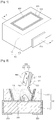
- FIG. 1 is a perspective view showing a light emitting device package according to the first embodiment
- FIG. 2 is a sectional view taken along line A-A' of FIG. 1
- FIG. 3 is a sectional view showing a light emitting chip.
- FIGS. 4 to 6 are sectional views showing the light emitting device package according to the modification of the first embodiment.
- the light emitting diode package includes a body 100, a plurality of lead electrodes 210 and 220, a light emitting part 300, a filling part 400, a reflective layer 500 and a light conversion layer 600.
- the body 100 receives the light emitting part 300, the filling part 400, the reflective layer 500, and the light conversion layer 600 and supports the lead electrodes 210 and 220.
- the body 100 may include any one among a resin material such as PPA, a ceramic material, a liquid crystal polymer (LCP), SPS (Syndiotactic), PPS (Poly(phenylene ether)), and a silicon material.
- a resin material such as PPA, a ceramic material, a liquid crystal polymer (LCP), SPS (Syndiotactic), PPS (Poly(phenylene ether)), and a silicon material.
- LCP liquid crystal polymer
- SPS Synchronastactic
- PPS Poly(phenylene ether)
- silicon material silicon material.
- the embodiment is not limited thereto.
- the body 100 may have an integral structure through an injection molding scheme, or a stack structure including a plurality of layers.
- the body 100 includes a cavity C having an open upper portion.
- the cavity C may be formed by performing a patterning, punching, cutting, or etching process with respect to the body 100.
- the cavity C may be formed by using a metallic frame having the shape of the cavity C when the body 100 is molded.
- the shape of the cavity C may include a cup shape, or a concave container shape.
- the surface of the cavity C may have a circular shape, a polygonal shape, or a random shape, but the embodiment is not limited thereto.
- An inner surface 122 of the cavity C may be perpendicular to a bottom surface of the cavity C or inclined with respect to the bottom surface of the cavity C based on the light emitting angle of the light emitting diode package.
- the body 100 includes a base part 110 and a receiving part 120.
- the base part 110 supports the receiving part 120.
- the base part 110 supports the lead electrodes 210 and 220.
- the base part 110 may have a rectangular shape.
- the receiving part 120 is provided on the base part 110.
- the cavity C is defined by the receiving part 120.
- the cavity C is a groove formed in the receiving part 120.
- the receiving part 120 surrounds the peripheral portion of the cavity C.
- the receiving part 120 may have the shape of a closed loop when viewed from the top.
- the receiving part 120 may have the shape of a wall surrounding the cavity C.
- the receiving part 120 includes a top surface, an outer surface 121, and the inner surface 122.
- the inner surface 122 is inclined with respect to the top surface 121.
- the lead electrodes 210 and 220 may be realized by using lead frames, but the embodiment is not limited thereto.
- the lead electrodes 210 and 220 are provided in the body 100.
- the lead electrodes 210 and 220 are electrically insulated from each other on the bottom surface of the cavity C.
- the outer portions of the lead electrodes 210 and 220 may be exposed outside the body 100.
- the end portions of the lead electrodes 210 and 220 may be provided at one side of the cavity C or an opposite side of the cavity C.
- the lead electrodes 210 and 220 may include lead frames.
- the lead frames may be formed when performing the injection-molding with respect to the body 100.
- the lead electrodes 210 and 220 may include the first lead electrode 210 and the second electrode 220.
- the first and second lead electrodes 210 and 220 are spaced apart from each other.
- the first and second lead electrodes 210 and 220 are electrically connected to the light emitting part 300.
- the light emitting part 300 includes at least one light emitting diode chip.
- the light emitting part 300 may include a color light emitting diode chip or an UV light emitting diode chip.
- the light emitting part 300 may include a horizontal light emitting diode chip or a vertical light emitting diode chip. As shown in FIG. 3 , the light emitting part 300 may include a conductive substrate 310, a light reflective layer 320, a first conductive semiconductor layer 330, a second conductive semiconductor layer 340, an active layer 350, and a second electrode 360.
- the conductive substrate 310 includes a conductor.
- the conductive substrate 310 supports the light reflective layer 320, the first conductive semiconductor layer 330, the second conductive semiconductor layer 340, the active layer 350, and a second electrode 360.
- the conductive substrate 310 is connected to the first conductive semiconductor layer 330 through the light reflective layer 320.
- the conductive substrate 310 serves as a first electrode to apply an electrical signal to the first conductive semiconductor layer 330.
- the light reflective layer 320 is provided on the conductive substrate 310.
- the light reflective layer 320 reflects upward light emitted from the active layer 350.
- the light reflective layer 320 is a conductive layer. Accordingly, the light reflective layer 320 connects the conductive substrate 310 to the first conductive semiconductor layer 330.
- the light reflective layer 320 may include metal such as silver (Ag) or aluminum (Al).
- the first conductive semiconductor layer 330 is provided on the light reflective layer 320.
- the first conductive semiconductor layer 330 has a first conductive type.
- the first conductive semiconductor layer 330 may include an N type semiconductor.
- the first conductive semiconductor layer 330 may include an N type GaN layer.
- the second conductive semiconductor layer 340 is provided on the first conductive semiconductor layer 330.
- the second conductive semiconductor layer 340 may face the first conductive semiconductor layer 330 and may include a P type semiconductor.
- the second conductive semiconductor layer 340 may include a P type GaN layer.
- the active layer 350 is interposed between the first and second conductive semiconductor layers 330 and 340.
- the active layer 350 has a single quantum well structure or a multiple-quantum well structure.
- the active layer 350 may be formed in the stack structure of an InGaN well layer and an AlGaN barrier layer, the stack structure of an InGaN well layer and a GaN barrier layer.
- the light emitting material of the active layer 350 may vary according to light emission wavelengths such as a blue wavelength, a red wavelength, or a green wavelength.
- the second electrode 360 is provided on the second conductive semiconductor layer 340.
- the second electrode 360 makes contact with the second conductive semiconductor layer 340.
- the light emitting part 300 may include a horizontal LED.
- the horizontal LED may require an additional wiring so that the horizontal LED is connected to the first lead electrode 210.
- the light emitting part 300 is connected to the first lead electrode 210 through a bump.
- the light emitting part 300 may be connected to the second lead electrode 220 through a wire.
- the light emitting part 300 may be directly provided on the first lead electrode 210.
- the light emitting part 300 may be connected to the lead electrodes through various connection schemes such as a wire bonding scheme, a die bonding scheme, or a flip-bonding scheme without the above connection scheme.
- connection schemes such as a wire bonding scheme, a die bonding scheme, or a flip-bonding scheme without the above connection scheme.
- the embodiment is not limited thereto.
- the filling part 400 is formed in the cavity C.
- the filling part 400 is transparent.
- the filling part 400 may include a material such as silicon or epoxy, or a material representing the reflective index of 2 or less.
- the filling part 400 covers the light emitting part 300.
- the filling part 400 may directly make contact with the light emitting part 300.
- the reflective layer 500 is provided in the body 100. In more detail, the reflective layer 500 is provided in the cavity C. In more detail, the reflective layer 500 may be provided on the inner surface 122 of the cavity C. In more detail, the reflective layer 500 may cover the inner surface 122 of the cavity C. Further, the reflective layer 500 may be directly provided on the inner surface 122 of the cavity C. The reflective layer 500 may be coated on the inner surface 122 of the cavity C.
- the reflective layer 500 may be formed on the entire portion of the inner surface 122 of the cavity C. In more detail, the reflective layer 500 may be provided on all of four inner surfaces of the cavity C. Therefore, the reflective layer 500 may surround the light emitting part 300, the filling part 400, and the light conversion layer 600. The reflective layer 500 may be formed on the bottom surface of the cavity C.
- the reflective layer 500 may include a material representing high reflectance.
- the reflective layer 500 may include white PSR (photo solder resist) ink, silver (Ag), or aluminum (Al).
- the light conversion layer 600 is provided in the cavity C.
- the light conversion layer 600 is provided adjacent to the reflective layer 500.
- the light conversion layer 600 may directly make contact with the reflective layer 500.
- the light conversion layer 600 may be provided on a reflective surface 510 of the reflective layer 500.
- the light conversion layer 600 may cover the reflective layer 500.
- the light conversion layer 600 may be formed on the entire portion of the reflective surface of the reflective layer 500.
- the light conversion layer 600 may surround the light emitting part 300 and the filling part 400. In other words, the light conversion layer 600 may surround a peripheral portion of the light emitting part 300.
- the internal width of the light conversion layer 600 may be increased as the light conversion layer 600 is farther away from the light emitting part 300.
- the light conversion layer 600 may have a radiation structure.
- the reflective layer 500 and the light conversion layer 600 may be inclined with respect to an optical axis OA of the light emitting part 600.
- the light conversion layer 600 is spaced apart from the light emitting part 300. Further, the light conversion layer 600 is spaced apart from the light emitting part 300, and the filling part 400 is provided between the light conversion layer 600 and the light emitting part 300. In addition, the light conversion layer 600 may directly make contact with the filling part 400.
- the light conversion layer 600 is spaced apart from the light emitting part 300, and provided between the light conversion part 300 and the inner surface 122 of the cavity C.
- the reflective layer 500 is provided between the light conversion layer 600 and the inner surface 122 of the cavity C.
- the light conversion layer 600 may be coated on the reflective surface 510 of the reflective layer 500.
- the thickness of the light conversion layer 600 may be in the range of about 0.5 ⁇ m to about 100 ⁇ m. In more detail, the thickness of the light conversion layer 600 may be in the range of about 1 ⁇ m to about 10 ⁇ m.
- the light conversion layer 600 receives the light from the light emitting part 300 to convert the wavelength of the light.
- the light conversion layer 600 may convert the incident blue light into the green light and the red light.
- the light conversion layer 600 may convert a part of the blue light into the green light having the wavelength in the range of about 520 nm to about 560 nm, and another part of the blue light into the red light having the wavelength in the range of about 630 nm to about 660 nm.
- the light conversion layer 600 may convert the UV light emitted from the light emitting part 300 into the blue light, the green light and the red light.
- the light conversion layer 600 may convert a part of the UV light into the blue light having the wavelength in the range of about 430 nm to about 470 nm, another part of the UV light into the green light having the wavelength in the range of about 520 nm to about 560 nm, and a part of the UV light into the red light having the wavelength in the range of about 630 nm to about 660 nm.
- the white light can be generated by the light passing through the light conversion layer 600 and the lights converted by the light conversion layer 600.
- the light emitting diode can output the white light through the combination of the blue, green, and red lights.
- the light conversion layer 600 includes a plurality of light conversion particles 610 and a host layer 620.
- the light conversion particles 610 are provided in the cavity C.
- the light conversion particles 610 are uniformly distributed in the host layer 620, and the host layer 620 is provided in the cavity C.
- the light conversion particles 610 convert the wavelength of light emitted from the light emitting part 300.
- the light conversion particles 610 receive the light emitted from the light emitting part 300 and convert the wavelength of the light.
- the light conversion particles 610 convert the blue light from the light emitting part 300 into the green light or the red light.
- a part of the light conversion particles 610 may convert the blue light into the green light having the wavelength in the range of about 520 nm to about 560 nm
- a part of the light conversion particles 610 may convert the blue light into the red light having the wavelength in the range of about 630 nm to about 660 nm.
- the light conversion particles 610 can convert the UV light emitted from the light emitting chip 300 into the blue light, the green light and the red light.
- a part of the light conversion particles 610 converts the UV light into the blue light having the wavelength in the range of about 430 nm to about 470 nm
- another part of the light conversion particles 610 converts the UV light into the green light having the wavelength in the range of about 520 nm to about 560 nm.
- a part of the light conversion particles 420 converts the UV light into the red light having the wavelength in the range of about 630 nm to about 660 nm.
- the light emitting part 300 emits blue light
- the light conversion particles 610 to convert the blue light into green and red lights may be used.
- the light emitting part 300 emits UV light
- the light conversion particles to convert the UV light into blue, green, and red lights may be used.
- the light conversion particles 610 may include a plurality of quantum dots.
- the quantum dots may include core nano-crystals and shell nano-crystals surrounding the core nano-crystals.
- the quantum dots may include organic ligands bonded with the shell nano-crystals.
- the quantum dots may include organic coating layers surrounding the shell nano-crystals.
- the shell nano-crystals may be prepared at least two layers.
- the shell nano-crystals are formed on the surface of the core nano-crystals.
- the quantum dots can lengthen the wavelength of the light incident into the core nano-crystals by using the shell nano-crystals forming a shell layer, thereby improving the light efficiency.
- the quantum dots may include at least one of a group-II compound semiconductor, a group-III compound semiconductor, a group-V compound semiconductor, and a group-VI compound semiconductor.
- the core nano-crystals may include CdSe, InGaP, CdTe, CdS, ZnSe, ZnTe, ZnS, HgTe or HgS.
- the shell nano-crystals may include CuZnS, CdSe, CdTe, CdS, ZnSe, ZnTe, ZnS, HgTe or HgS.
- the diameter of the quantum dot may be in the range of 1 nm to 10 nm.
- the wavelength of the light emitted from the quantum dots can be adjusted according to the size of the quantum dot or the molar ratio between the molecular cluster compound and the nano-particle precursor in the synthesis process.
- the organic ligand may include pyridine, mercapto alcohol, thiol, phosphine and phosphine oxide.
- the organic ligand may stabilize the unstable quantum dots after the synthesis process. Dangling bonds may be formed at the valence band and the quantum dots may be unstable due to the dangling bonds. However, since one end of the organic ligand is the non-bonding state, one end of the organic ligand is bonded with the dangling bonds, thereby stabilizing the quantum dots.
- the size of the quantum dot is smaller than the Bohr radius of an exciton, which consists of an electron and a hole excited by light and electricity, the quantum confinement effect may occur, so that the quantum dot may have the discrete energy level.
- the size of the energy gap is changed.
- the charges are confined within the quantum dot, so that the light emitting efficiency can be improved.
- the fluorescent wavelength of the quantum dot may vary depending on the size of the particles.
- the light has the shorter wavelength as the size of the particle is reduced, so that the phosphorous light having the wavelength band of visible ray can be generated by adjusting the size of the particles.
- the quantum dot represents the extinction coefficient which is 100 to 1000 times higher than that of the general phosphorous pigment and has the superior quantum yield as compared with the general fluorescent pigment, so that strong fluorescent light can be generated.
- the quantum dots can be synthesized through the chemical wet scheme.
- the chemical wet scheme is to grow the particles by immersing the precursor material in the organic solvent. According to the chemical wet scheme, the quantum dots can be synthesized.
- the host layer 620 is provided on the reflective layer 500.
- the host layer 620 may be coated on the entire portion of the reflective surface 510 of the reflective layer 500.
- the host layer 620 may adhere to the reflective layer 500.
- the host layer 620 surrounds the light conversion particles 610. In other words, the host layer 620 uniformly distributes the light conversion particles 610 therein.
- the host layer 620 may include polymer.
- the host layer 620 is transparent.
- the host layer 620 may include transparent polymer.
- the host layer 620 may include a thermosetting resin or a photo-curable resin.
- the host layer 620 may include silicon-based resin or epoxy-based resin.
- the reflective layer 500 is provided adjacent to the light conversion layer 600. Accordingly, after the wavelength of the light emitted from the light emitting part 300 has been incident into the light conversion layer 600, the wavelength of the light may be instantly converted. In addition, the wavelength of the light emitted from the light emitting part 300 may be converted after the light has passed through the light conversion layer 600, reflected by the reflective layer 500, and re-incident into the light absorbing layer.
- the wavelength of the light emitted from the light emitting part 300 can be effectively converted by forming the light conversion layer 600 on the reflective layer 500.
- the light conversion layer 600 may be formed on a region adjacent to the reflective layer 500, for example, only on the reflective surface 510 of the reflective layer 500 without forming on the internal entire portion of the cavity C. Therefore, according to the light emitting diode package of the first embodiment, the use of the light conversion particles 610 such as quantum dots used in the light conversion layer 600 may be reduced. Therefore, the light emitting diode package according to the first embodiment may be easily fabricated at a low cost
- the light conversion layer 600 is formed on the inner surface 122 of the cavity C while being spaced apart from the light emitting part 300. Therefore, the light conversion layer 600 may be prevented from being degraded due to heat emitted from the light emitting part 300. Accordingly, the light emitting diode package according to the first embodiment may represent improved reliability and improved durability.
- the light emitting diode package according to the first embodiment further includes a reflective part 700.
- the reflective part 700 is provided adjacent to the optical axis OA of the light emitting part 300.
- the reflective part 700 is provided adjacent to the optical axis OA of the light emitting part 300.
- the reflective part 700 may be provided in the cavity C.
- the reflective part 700 may be provided in the filling part 400.
- the reflective part 700 may be integrally formed with the filling part 400.
- the reflective part 700 may include a material representing high reflectance.
- the reflective part 700 may include representing reflectance very higher than that of the material constituting the filling part 400.
- the reflective part 700 may include white PSR (photo solder resist) ink, silver (Ag), or aluminum (Al).
- the reflective part 700 reflects light emitted from the light emitting part 300.
- the reflective part 700 may reflect light emitted from the light emitting part 300 in a side direction.
- the reflective part 700 may reflect the light emitted from the light emitting part 300 to the light conversion part 600.
- the reflective part 700 may have the shape of a plate.
- the center of the reflective part 700 may be provided on the optical axis OA of the light emitting part 300.
- the reflective part 700 may have a conical shape.
- the vertex of the reflective part 700 is directed toward the light emitting part 300.
- the vertex of the reflective part 700 may be provided on the optical axis OA of the light emitting part 300.
- the vertex of the reflective part 700 is directed toward the light emitting part 300.
- a recess part 401 may be formed in the filling part 400.
- the recess part 401 may be recessed toward the light emitting part 300. Therefore, an inner surface 401 of the recess part 401 may serve as a total reflection surface 510.
- the inner surface 410 of the recess part 401 is inclined with respect to the optical axis OA of the light emitting part 300.
- the light emitted from the light emitting part 300 toward the recess part 401 may be reflected in the side direction due to the inner surface 410 of the recess part 401.
- the reflective part 700 and the recess part 401 reflect light emitted from the light emitting part 300 toward the light conversion layer 600. Accordingly, the greater amount of light can be incident into the light conversion layer 600 by the reflective part 700 and the recess part 401.
- the light emitting package according to the first embodiment may represent improved color reproducibility.
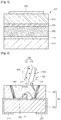
- FIG. 7 is a perspective view showing a light emitting device package according to the second embodiment
- FIG. 8 is a sectional view taken along lien A-A' of FIG. 7
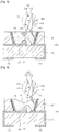
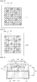
- FIGS. 9 to 11 are plan views showing a light conversion part.
- FIG. 13 is a plan view showing a heat transfer part
- FIG. 14 is a sectional view showing a light emitting device package according to another embodiment
- FIG. 15 is a sectional view showing a light emitting device package according still another embodiment.
- FIG. 16 is a sectional view showing a light emitting device package according to still another embodiment.
- the light emitting device package includes a body 1000, a plurality of lead electrodes 2100 and 2200, a light emitting part 3000, a first capping part 4100, a light conversion part 5000, and a second capping part 4200.
- the body 1000 receives the light emitting part 3000, the filling part 4000, a reflective layer, and the light conversion part 5000 and supports the lead electrodes 2100 and 2200.
- the body 1000 may include any one among a resin material such as PPA, a ceramic material, a liquid crystal polymer (LCP), SPS(Syndiotactic), PPS(Poly(phenylene ether)), and a silicon material.
- a resin material such as PPA
- a ceramic material such as a ceramic material
- LCP liquid crystal polymer
- SPS(Syndiotactic) SPS(Poly(phenylene ether)
- silicon material such as silicon
- the embodiment is not limited thereto.
- the body 1000 may have an integral structure through an injection molding scheme, or a stack structure including a plurliaty of layers.
- the body 1000 includes a cavity C having an open upper portion.
- the cavity C may be formed by performing a patterning, punching, cutting, or etching process with respect to the body 1000.
- the cavity C may be formed by using a metallic frame having the shape of the cavity C when the body 1000 is molded.
- the shape of the cavity C may include a cup shape, or a concave container shape.
- the surface of the cavity C may have a circular shape, a polygonal shape, or a random shape, but the embodiment is not limited thereto.
- An inner surface of the cavity C may be perpendicular to a bottom surface of the cavity C or inclined with respect to the bottom surface of the cavity C based on the light emission angle of the light emitting diode package.
- the body 1000 includes a base part 1100 and a receiving part 1200.
- the base part 1100 supports the receiving part 1200.
- the base part 1100 supports the lead electrodes 2100 and 2200.
- the base part 1100 may have a rectangular shape.
- the receiving part 1200 is provided on the base part 1200.
- the cavity C is defined by the receiving part 1200.
- the cavity C is a groove formed in the receiving part 1200.
- the receiving part 1200 surrounds the peripheral portion of the cavity C.
- the receiving part 1200 may have the shape of a closed loop when viewed from the top.
- the receiving part 1200 may have the shape of a wall surrounding the cavity C.
- the receiving part 1200 includes a top surface, an outer surface, and an inner surface.
- the inner surface is inclined with respect to the top surface.
- the lead electrodes 2100 and 2200 may be realized by using lead frames, but the embodiment is not limited thereto.
- the lead electrodes 2100 and 2200 are provided in the body 1000.
- the lead electrodes 2100 and 2200 are electrically insulated from each other on the bottom surface of the cavity C.
- the outer portions of the lead electrodes 2100 and 2200 may be exposed outside the body 100.
- the end portions of the lead electrodes 2100 and 220 may be provided at one side of the cavity C or an opposite side of the cavity C.
- the lead electrodes 2100 and 2200 may include lead frames.
- the lead frames may be formed when performing the injection-molding with respect to the body 100.
- the lead electrodes 2100 and 2200 may include the first lead electrode 2100 and the second electrode 2200.
- the first and second lead electrodes 2100 and 2200 are spaced apart from each other.
- the first and second lead electrodes 2100 and 2200 are electrically connected to the light emitting part 3000.
- the light emitting part 3000 includes at least one light emitting diode chip.
- the light emitting part 3000 may include a color light emitting diode chip or an UV light emitting diode chip.
- the light emitting part 3000 may include a horizontal light emitting diode chip or a vertical light emitting diode chip. As shown in FIG. 3 , the light emitting part 3000 may include a conductive substrate 310, a light reflective layer 320, a first conductive semiconductor layer 330, a second conductive semiconductor layer 340, an active layer 350, and a second electrode 360. In other words, the description of the light emitting part provided in the light emitting device package according to the second embodiment will be incorporated in the description of the light emitting part of the light emitting device package according to the first embodiment.
- the light emitting part 3000 may be connected to the first lead electrode 2100 through a bump.
- the light emitting part 3000 may be connected to the second lead electrode 2200 through a wire.
- the light emitting part 3000 may be directly provided on the first lead electrode 2100.
- the light emitting part 3000 may be connected to the lead electrodes through various connection schemes such as a wire bonding scheme, a die bonding scheme, or a flip-bonding scheme without the above connection scheme.
- connection schemes such as a wire bonding scheme, a die bonding scheme, or a flip-bonding scheme without the above connection scheme.
- the embodiment is not limited thereto.
- the reflective layer may be provided in the cavity C.
- the reflective layer may be provided on the inner surface of the cavity C.
- the reflective layer may be coated on the inner surface of the cavity C.
- the reflective layer may include a material representing high reflectance.
- the reflective layer may include white PSR ink, silver (Ag), or aluminum (Al).
- the first capping part 4100 is provided in the cavity C.
- the first capping part 4100 covers the light emitting part 3000.
- the first capping part 4100 is provided on the bottom surface of the cavity C.
- the first capping part 4100 covers the top surface and the lateral side of the light emitting part 3000.
- the first capping part 4100 covers a portion of the lead electrodes 2100 and 2200.
- the first capping part 4100 may include a curved surface.
- the top surface of the first capping part 4100 directed toward the open upper portion of the cavity C may include a curved surface.
- the top surface of the first capping part 4100 may include a curved surface that is totally convex.
- the first capping part 4100 may seal the light emitting part 3000.
- the first capping part 4100 may protect the light emitting part 3000.
- the first capping part 4100 is transparent.
- the first capping part 4100 may include a material representing the refractive index of 2 or less.
- the first capping part 4100 may include silicon-based resin, or epoxy-based resin.
- the first capping part 4100 serves as a spacer to space the light conversion part 5000 apart from the light emitting part 3000.
- the first capping part 4100 is interposed between the light emitting part 3000 and the light conversion part 5000 to perform an adiabatic function.
- the first capping part 4100 may include a material representing lower thermal conductivity.
- the first capping part 4100 may have thermal conductivity lower than that of the second capping part 4200. Accordingly, the heat emitted from the light emitting part 3000 may be efficiently blocked by the first capping part 4100.
- the light conversion part 5000 is provided in the cavity C.
- the light conversion part 5000 is provided on the path of the light emitted from the light emitting part 3000.
- the light conversion part 5000 is provided on the light emitting part 3000.
- the light conversion part 5000 is provided on at least one surface of the first capping part 4100.
- the light conversion part 5000 is provided on the top surface of the first capping part 4100.
- the light conversion part 5000 may be provided on the curved surface of the first capping part 4100.
- the light conversion part 5000 may be directly provided on the curved surface of the first capping part 4100.
- the light conversion part 5000 receives light emitted from the light emitting part 3000 to convert the wavelength of the light.
- the light conversion part 5000 can convert the incident blue light into the green light and the red light. That is, the light conversion part 5000 converts a part of the blue light into the green light having the wavelength in the range of about 520 nm to about 560 nm and converts another part of the blue light into the red light having the wavelength in the range of about 630 nm to about 660 nm.
- the light conversion part 5000 may convert the incident blue light into yellow, green, and red light.
- the light conversion part 5000 may convert UV light emitted from the light emitting part 3000 into blue, green, and red light.
- the light conversion part 5000 converts a part of the UV light into the blue light having the wavelength in the range of about 430 nm to about 470 nm, converts another part of the UV light into the green light having the wavelength in the range of about 520 nm to about 560 nm, and another part of the UV light into the red light having the wavelength in the range of about 630 nm to about 660 nm.
- the white light can be generated by the light converted by the light conversion part 5000 or the light passing through the light conversion part 5000.
- the white light can be emitted through the combination of the blue, green, and red lights.
- the light conversion part 5000 includes a plurality of light conversion lens parts 5100, 5200, and 5300.
- the light conversion part 5000 may include the first light conversion lens part 5100, the second light conversion lens part 5200, and the third light conversion lens part 5300.
- the first light conversion lens part 5100 is provided on the first capping part 4100.
- the first light conversion lens part 5100 is provided on the top surface of the first capping part 4100.
- the first light conversion lens part 5100 may be provided on the curved surface of the first capping part 4100.
- the first light conversion lens part 5100 has a curved surface 5130.
- the first light conversion lens part 5100 may have a curved surface 5130 which is convex toward the open part, that is, upward.
- the curved surface 5130 of the first light conversion lens part 5100 may include a spherical surface or an aspherical surface.
- the first light conversion lens part 5100 may include a concave surface.
- the first light conversion lens part 5100 may include a surface which is concave toward the light emitting part 3000.
- the first light conversion lens part 5100 may convert the light emitted from the light emitting part 3000 into the light having the first wavelength band.
- the first light conversion lens part 5100 may convert incident light into green light.
- the first light conversion lens part 5100 may convert the UV light or the blue light emitted from the light emitting part 3000 into green light having the wavelength band in the range of about 520 nm to about 560 nm.
- the first light conversion lens part 5100 includes a plurality of first light conversion particles 5110 and a first matrix 5120.
- the first light conversion particles 5110 may convert the UV light or the blue light emitted from the light emitting part 3000 into green light having the wavelength band. In other words, the first light conversion particles 5110 may convert the UV light or the blue light into green light having the wavelength band in the range of about 520 nm to about 560 nm.
- the first light conversion particles 5110 may include a plurality of quantum dots.
- the quantum dots may include core nano-crystals and shell nano-crystals surrounding the core nano-crystals.
- the quantum dots may include organic ligands bonded to the shell nano-crystals.
- the quantum dots may include an organic coating layer surrounding the shell nano-crystals.
- the shell nano-crystals can be prepared as at least two layers.
- the shell nano-crystals are formed on the surface of the core nano-crystals.
- the quantum dots lengthen the wavelength of the light incident into the core nano-crystals by using the shell nano-crystals forming a shell layer, thereby improving the light efficiency.
- the quantum dots may include at least one of a group-II compound semiconductor, a group-III compound semiconductor, a group-V compound semiconductor, and a group-VI compound semiconductor.
- the core nano-crystals may include CdSe, InGaP, CdTe, CdS, ZnSe, ZnTe, ZnS, HgTe or HgS.
- the shell nano-crystals may include CuZnS, CdSe, CdTe, CdS, ZnSe, ZnTe, ZnS, HgTe or HgS.
- the quantum dot may have a diameter of about 1nm to about 10 nm.
- the wavelength of the light emitted from the quantum dots can be adjusted according to the size of the quantum dot or the molar ratio between the molecular cluster compound and the nano-particle precursor in the synthesis process.
- the organic ligand may include pyridine, mercapto alcohol, thiol, phosphine and phosphine oxide.
- the organic ligand may stabilize the unstable quantum dots after the synthesis process. Dangling bonds may be formed at the valence band and the quantum dots may be unstable due to the dangling bonds. However, since one end of the organic ligand is the non-bonding state, one end of the organic ligand is bonded with the dangling bonds, thereby stabilizing the quantum dots.
- the size of the quantum dot is smaller than the Bohr radius of an exciton, which consists of an electron and a hole excited by light and electricity, the quantum confinement effect may occur, so that the quantum dot may have the discrete energy level.
- the size of the energy gap is changed.
- the charges are confined within the quantum dot, so that the light emitting efficiency can be improved.
- the fluorescent wavelength of the quantum dot may vary depending on the size of the particles.
- the light has the shorter wavelength as the size of the particle becomes small, so the fluorescent light having the wavelength band of visible ray can be generated by adjusting the size of the particles.
- the quantum dot represents the extinction coefficient higher than that of the general fluorescent pigment by 100 to 1000 times and has the superior quantum yield, so that strong fluorescent light can be generated.
- the quantum dots can be synthesized through the chemical wet scheme. According to the chemical wet scheme, the particles are grown by immersing the precursor material in the organic solvent. The quantum dots can be synthesized through the chemical wet scheme.
- the first light conversion particles 5110 may include green phosphors.
- the green phosphors may include zinc silicon oxide phosphors doped with Mn (e.g., Zn 2 SiO 4 :Mn), strontium gallium sulfide phosphors doped with europium (e.g., SrGa 2 S 4 :Eu), or barium silicon oxide chloride phosphors doped with europium (e.g., Ba 5 Si 2 O 7 Cl 4 :Eu).
- the first matrix 5120 receives the first light conversion particles 5110.
- the first matrix 5120 surrounds the first light conversion particles 5110.
- the first matrix 5120 distributes the first light conversion particles 5110.
- the first matrix 5120 is transparent.
- the first matrix 5120 may have a lens shape.
- the outer shape of the first light conversion lens part 5100 may be realized by the first matrix 5120.
- the first matrix 5120 may include silicon-based resin or epoxy-based resin.
- the second light conversion lens part 5200 is provided on the first capping part 4100.
- the second light conversion lens part 5200 is provided on the top surface of the first capping part 4100.
- the second light conversion lens part 5200 may be provided on the curved surface of the first capping part 4100.
- the second light conversion lens part 5200 is provided beside the first light conversion lens part 5100.
- the first and second light conversion lens parts 5100 and 5200 may be provided on the same plane and may be adjacent to each other.
- the second light conversion lens part 5200 has a curved surface 5230.
- the second light conversion lens part 5200 may have a curved surface 5230 which is convex toward the open part, that is, upward.
- the curved surface 5230 of the second light conversion lens part 5200 may include a spherical surface or an aspherical surface.
- the second light conversion lens part 5200 may include a concave surface.
- the second light conversion lens part 5200 may include a surface which is concave toward the light emitting part 3000.
- the second light conversion lens part 5200 may convert the light emitted from the light emitting part 3000 into light having a second wavelength band.
- the second light conversion lens part 5200 may convert the incident light into red light.
- the second light conversion lens part 5200 may convert the UV light or the blue light emitted from the light emitting part 3000 into red light having the wavelength band of about 630 nm to about 660 nm.
- the second light conversion lens part 5200 includes a plurality of second light conversion particles 5210 and a second matrix 5220.
- the second light conversion particles 5210 may convert the blue light or UV light emitted from the light emitting part 3000 into red light.
- the second light conversion particles 5210 may convert the UV light or the blue light into the red light having the wavelength band of about 630 nm to about 660 nm.
- the second light conversion particles 5210 may include a plurality of red quantum dots.
- the quantum dots used as the second light conversion particles 5210 may have the diameter of about 4 nm to about 10 nm so that the incident light into red light.
- the second light conversion particles 5210 may include red phosphors.
- the red phosphors may include strontium titanium oxide phosphors doped with praseodymium (e.g., SrTiO 3 : Pr, Al) or calcium titanium oxide phosphors (e.g., CaTiO 3 : Pr) doped with praseodymium.
- the second matrix 5220 receives the second light conversion particles 521.
- the second matrix 5220 surrounds the second light conversion particles 521.
- the second matrix 5220 disperses the second light conversion particles 5210.
- the second matrix 5220 is transparent.
- the second matrix 5220 may have a lens shape.
- the outer shape of the second light conversion lens part 5200 may be realized by the second matrix 5220.
- the second matrix 5220 may include silicon-based resin or epoxy-based resin.
- the third light conversion lens part 5300 is provided on the first capping part 4100.
- the third light conversion lens part 5300 is provided on the top surface of the first capping part 4100.
- the third light conversion lens part 5300 may be provided on the curved surface of the first capping part 4100.
- the third light conversion lens part 5300 is provided beside the first light conversion part 5100.
- the third light conversion lens part 5300 is provided beside the second light conversion lens part 5200.
- the first to third light conversion lens parts 5100 to 5300 may be provided on the same plane, and may be adjacent to each other.
- the third light conversion lens part 5300 has a curved surface 5330.
- the third light conversion lens part 5300 may have a curved surface 5330 which is convex toward the open part, that is, upward.
- the curved surface 5330 of the third light conversion lens part 5300 may include a spherical surface or an aspherical surface.
- the third light conversion lens part 5300 may include a concave surface.
- the third light conversion lens part 5300 may include a surface which is concave toward the light emitting part 3000.
- the third light conversion lens part 5300 may convert light emitted from the light emitting part 3000 to light having a third wavelength band. For example, if the UV light is emitted from the light emitting part 3000, the third light conversion lens part 5300 may convert the UV light into blue light. In more detail, the third light conversion lens part 5300 may convert the UV light emitted from the light emitting part 3000 into the blue light having the wavelength band in the range of about 430 nm to about 470 nm.
- the third light conversion lens part 5300 may convert the blue light emitted from the light emitting part 3000 into yellow light.
- the third light conversion lens part 5300 includes a plurality of third light conversion particles 5310 and a third matrix 5320.
- the third light conversion particles 5310 may convert the UV light emitted from the light emitting part 3000 into blue light. In other words, the third light conversion particles 5310 may convert the UV light into the blue light having the wavelength band in the range of about 430 nm to about 470 nm.
- the third light conversion particles 5310 may include a plurality of red quantum dots.
- the quantum dots used as the third light conversion particles 5310 may have the diameter of about 1 nm to about 2 nm so that the incident light into blue light.
- the third light conversion particles 5310 may include a blue phosphor.
- the third light conversion particles 5310 may convert the blue light emitted from the light emitting part 3000 into yellow light.
- the third light conversion particles 5310 may include a yellow phosphor such as a YAG phosphor.
- the third matrix 5320 receives the third light conversion particles 5310.
- the third matrix 5320 surrounds the third light conversion particles 5310.
- the third matrix 5320 distributes the third light conversion particles 5310.
- the third matrix 5320 is transparent.
- the second matrix 5320 may have a lens shape.
- the outer shape of the third light conversion lens part 5300 may be realized by the third matrix 5320.
- the third matrix 5320 may include silicon-based resin or epoxy-based resin.
- transmissive regions TA may be formed between the first and second light conversion lens parts 5100 and 5200, and between the second and third light conversion lens parts 5200 and 5300.
- the transmissive regions TAs allow the light emitted from the light emitting part 3000 to directly pass therethrough without being converted.
- the color coordinates of the light emitting device according to the embodiment can be properly adjusted by adjusting the area of the transmissive regions TA.
- the transmissive regions TAs may be defined in peripheral regions of the first to third light conversion lens parts 5100 to 5300.
- the first to third light conversion lens parts 5100 to 5300 emit lights having wavelength bands different from each other.
- the first to third light conversion lens parts 5100 to 5300 may be differently designed.
- the first to third light conversion lens parts 5100 to 5300 may be designed so that the optical characteristics of the first to third light conversion lens parts 5100 to 5300 are suitable to lights of the wavelength bands thereof, respectively.
- the sizes, the shapes, and the refractive indexes of the first to third light conversion lens parts 5100 to 5300 may be adjusted suitably for the lights of the wavelength bands thereof.
- the light conversion lens part emitting the light having a longer wavelength band may be designed with a less orientation angle.
- the light conversion lens part emitting the light having a shorter wavelength band may be designed with a great orientation angle.
- the sizes and the radiuses of curvature of the first to third light conversion part 5100 to 5300 and the concentration of the light conversion particles 5100, 5210, and 5310 can be properly adjusted. Accordingly, the light emitting device according to the embodiment may emit lights representing required characteristics according to the wavelength bands.
- the light emitting device can easily adjust the color coordinates by adjusting the sizes of the first to third light conversion lens parts 5100 to 5300.
- the first to third light conversion lens parts 5100 to 5300 may constitute a light conversion pattern.
- the light conversion part 5000 includes the light conversion pattern.
- the light conversion part 5000 may include the light conversion lens parts 5100 to 5300 that are uniformly repeated.
- the light conversion pattern includes the light conversion lens parts 5100 to 5300 provided on the entire portion of the top surface of the first capping part 4100. As shown in FIG. 10 , the light conversion lens parts 5100, 5200, and 5300 may have a circular shape. As shown in FIG. 11 , the light conversion lens parts 5100 to 5300 may have a rectangular shape.
- the light conversion lens parts 5100, 5200, and 5300 may include a plurality of first light conversion lens parts 5100, a plurality of second light conversion lens parts 5200, and a plurality of third light conversion lens parts 5300.
- the first light conversion lens parts 5100 may emit green light
- the second light conversion lens parts 5200 may emit red light
- the third light conversion lens parts 5300 may emit blue light or yellow light.
- the first to third light conversion lens parts 5100 to 5300 may be alternately arranged.
- the first light conversion lens parts 5100 are provided at the center of the light conversion part 5000, and the second light conversion lens parts 5200 may be provided at the outer portions of the light conversion part 5000.
- the first light conversion lens parts 5100 are closer to the optical axis of the light emitting part 3000, and the second light conversion lens parts 5200 may be provided farther away from the optical axis of the light emitting part 3000.
- the light emitting device can emit light having a required wavelength band at a required position from the optical axis of the light emitting part 3000.
- the light emitting device can properly adjust the positions according to the required wavelength bands by using the light conversion pattern.
- first to third light conversion lens parts 5100 to 5300 may have a diameter of about 10 ⁇ m to about 1 mm.
- the second capping part 4200 covers the light conversion part 5000.
- the second capping part 4200 is provided in the cavity C.
- the second capping part 4200 seals the light conversion part 5000.
- the second capping part 4200 covers the light conversion lens parts 5100 to 5300.
- the second capping part 4200 covers the curved surfaces of the light conversion lens parts 5100 to 5300. In more detail, the second capping part 4200 directly makes contact with the light conversion lens parts 5100 to 5300.
- the second capping part 4200 is transparent.
- the second capping part 4200 may include an inorganic material.
- the second capping part 4200 may include silicon oxide or indium tin oxide.
- the second capping part 4200 may have higher thermal conductivity.
- the second capping part 4200 may have thermal conductivity higher than that of the first capping part 4100.
- the second capping part 4200 may have thermal conductivity higher than that of the light conversion part 5000.
- the light conversion lens parts 5100, 5200, and 5300 include convex curved surfaces 5130, 5230, and 5330. Therefore, the contact area between the light conversion lens parts 5100, 5200, and 5300 and the second capping part 4200 is increased, and the heat emitted from the light conversion lens parts 5100, 5200, and 5300 may be easily discharged through the second capping part 4200.
- the light emitting device can reduce the performance degradation caused by the heat, and can represent improved reliability and durability.
- the light emitting device can emit white light representing improved optical characteristics by using the light conversion lens parts 5100, 5200, and 5300.
- FIG. 12 is a sectional view showing a light emitting device package according to an embodiment of the invention.
- FIG. 13 is a plan view showing a heat transfer part.
- FIG. 14 is a sectional view showing a light emitting device package according to still another embodiment of the invention.
- the present embodiments will be described by making reference to the above description of the light emitting device packages. In other words, the description of the light emitting device package may be incorporated in the description of the present embodiment except for the modifications.
- the light emitting device package according to the present embodiment includes a heat transfer part 6000.
- the heat transfer part 6000 is interposed between the light conversion part 5000 and the light emitting part 3000.
- the heat transfer part 6000 may represent high thermal conductivity.
- the heat transfer part 6000 is provided in the first capping part 4100. In this case, the heat transfer part 6000 is provided at the intermediate region of the first capping part 4100.
- the first capping part 4100 may be divided into a first adiabatic part 4110 and a second adiabatic part 4120.
- the heat transfer part 6000 may represent thermal conductivity higher than that of the first capping part 4100.
- the first and second adiabatic parts 4110 and 4120 represent thermal conductivity lower than that of the heat transfer part 6000.
- the first and second adiabatic parts 4110 and 4120 sandwich the heat transfer part 6000 therebetween.
- the heat transfer part 6000 may include a material representing high thermal conductivity.
- the heat transfer part 6000 may include indium tin oxide, aluminum (Al), or silver (Ag) representing high reflectance.
- the heat transfer part 6000 may have the shape of a mesh.
- the heat transfer part 6000 includes a transmissive part T allowing light to pass therethrough.
- the heat transfer part 6000 allows light to pass therethrough.
- the heat transfer part 6000 is connected to the body 1000.
- the heat transfer part 6000 is connected to a heat radiation member (not shown) provided in the body 1000. Therefore, the heat transfer part 6000 may effectively discharge heat emitted from the light emitting part 3000 to the outside.
- first and second heat radiation parts 4110 and 4120 are coupled with the heat transfer part 6000, so that the first and second heat radiation parts 4110 and 4120 can effectively block heat.
- the first adiabatic part 4110 can primarily block the heat emitted from the light emitting part 3000, and the second adiabatic part 4120 can effectively block remaining heat after the heat is discharged through the heat transfer part 6000.
- the heat transfer part 6000 may include a transparent layer.
- the heat transfer part 6000 may include a transparent conductive layer.
- the heat transfer part 6000 may include indium tin oxide or zinc oxide doped with metal.
- the light emitting diode package according to the embodiment can effectively block and discharge heat emitted from the light emitting part 3000, thereby preventing the light conversion part 5000 from being degraded.
- the light emitting diode package according to the embodiment can represent improved reliability and durability.
- FIG. 15 is a sectional view showing the light emitting device package according to still another embodiment.
- the present embodiments will be described by making reference to the above description of the light emitting device packages.
- the description of the light emitting device package may be incorporated in the description of the present embodiment except for the modifications.
- the light conversion part 5000 may be provided outside the body 1000.
- the light conversion part 5000 may be provided outside the cavity C of the body 1000.
- the first capping part 4100 may be filled in the entire portion of the cavity C.
- the light conversion lens parts 5100, 5200, and 5300 constituting the light conversion part 5000 is provided outside the cavity C.
- the second capping part 4200 may cover the light conversion lens parts 5100, 5200, and 5300 in the form of a thin film.
- the second capping part 4200 may have the same shape as that of the light conversion lens parts 5100, 5200, and 5300. In other words, the second capping part 4200 may have the same curved surface as that of the light conversion lens parts 5100, 5200, and 5300.
- the light emitting device package according to the present embodiment can freely adjust the optical characteristics of the light conversion lens parts 5100, 5200, and 5300 without the influence of the second capping part 4200.
- the light conversion part 5000 since the light conversion part 5000 is provided outside the cavity C, the light conversion part 5000 may not be damaged due to the heat emitted from the light emitting part 3000.
- the light emitting device package according to the embodiment can represent improved reliability and improved durability.
- FIG. 16 is a sectional view showing the light emitting device package according to still another embodiment.
- the present embodiments will be described by making reference to the above description of the light emitting device packages.
- the description of the light emitting device package may be incorporated in the description of the present embodiment except for the modifications.
- the light emitting device package includes a substrate 1300, two lead electrodes 2100 and 2200, a light emitting part 3000, a heat radiation part 6020, light conversion parts 5100, 5200, and 5300, and a capping part 4300.
- the substrate 1300 supports the lead electrodes 2100 and 2200, the light emitting part 3000, the heat radiation part 6020, the light conversion parts 5100, 5200, and 5300, and the capping part 4300.
- the substrate 1300 includes an insulator.
- the substrate 1300 may have the shape of a plate.
- the substrate 1300 may include a polymer substrate and a glass substrate. In more detail, the substrate 1300 may include epoxy resin.
- the lead electrodes 2100 and 2200 may pass through the substrate 1300.
- the lead electrodes 2100 and 2200 may extend from the top surface of the substrate 1300 to the bottom surface thereof.
- the lead electrodes 2100 and 2200 and the substrate 1300 may be formed through an overmolding process.
- the light emitting part 3000 is provided on the substrate 1300.
- the light emitting part 3000 is electrically connected to the lead electrodes 2100 and 2200.
- the heat radiation part 6020 is provided on the substrate 1300.
- the heat radiation part 6020 covers the light emitting part 3000.
- the heat radiation part 6020 covers the lateral side and the top surface of the light emitting part 3000.
- the heat radiation part 6020 may directly make contact with the light emitting part 3000.
- the heat radiation part 6020 may directly make contact with the lead electrodes 2100 and 2200.
- the heat radiation part 6020 discharges heat emitted from the light emitting part 3000 to the outside.
- the heat radiation part 6020 may discharge the heat emitted from the light emitting part 3000 in a side direction.
- the heat radiation part 6020 may be formed by laminating a plurality of thin films.
- the heat radiation part 6020 may be formed by laminating thin films having thermal conductivities different from each other.
- the heat radiation part 6020 has a thickness of about 1 ⁇ m to about 1mm.
- the heat radiation part 6020 includes a first heat conductive layer 6100, a first adiabatic layer 6200, a second heat conductive layer 6300, and a second adiabatic layer 6400.
- the first heat conductive layer 6100 is provided on the substrate 1300.
- the first heat conductive layer 6100 covers the light emitting part 3000.
- the first heat conductive layer 6100 covers the top surface of the substrate 1300.
- the first heat conductive layer 6100 covers the top surface and the lateral side of the light emitting part 3000.
- the first heat conductive layer 6100 may directly make contact with the light emitting part 3000.
- the first heat conductive layer 6100 may extend to the lateral side of the substrate 1300. In more detail, the first heat conductive layer 6100 may extend the lateral side and the bottom surface of the substrate 1300.
- the first heat conductive layer 6100 has a thickness of about 1 ⁇ m to about 500 ⁇ m.
- the first heat conductive layer 6100 includes a first heat transfer part 6110 and a first heat discharge part 6120.
- the first heat transfer part 6110 is covered by the first adiabatic layer 6200.
- the first heat transfer part 6110 corresponds to the first adiabatic layer 6200.
- the first heat transfer part 6110 directly makes contact with the first adiabatic layer 6200.
- the first heat discharge part 6120 is exposed by the first adiabatic layer 6200.
- the first heat discharge part 6120 is integrally formed with the first heat transfer part 6110.
- the first heat discharge part 6120 may be exposed to the air.
- the heat emitted from the heat radiation part 6020 is transferred to the first heat discharge part 6120 through the first heat transfer part 6110.
- the first heat discharge part 6120 may discharge the heat transferred from the first heat transfer part 6110 to the air.
- the first adiabatic layer 6200 is provided on the first heat conductive layer 6100.
- the first adiabatic layer 6200 covers a part of the top surface of the first heat conductive layer 6100.
- the first adiabatic layer 6200 is directly provided on the top surface of the first heat conductive layer 6100.
- the first adiabatic layer 6200 exposes a portion of the first heat conductive layer 6100. In other words, the first adiabatic layer 6200 covers the first heat conductive layer 6100 while exposing the first heat discharge part 6120.
- the first adiabatic layer 6200 may have a thickness of about 1 ⁇ m to about 500 ⁇ m.
- the second heat conductive layer 6300 is provided on the first adiabatic layer 6200.
- the third heat conductive layer 6300 covers the top surface of the first adiabatic layer 6200.
- the second heat conductive layer 6300 may directly make contact with the first adiabatic layer 6200.
- the second thermal conductive layer 6300 has a thickness of about 1 ⁇ m to about 500 ⁇ m.
- the second heat conductive layer 6300 includes a second heat transfer part 6310 and a second heat discharge part 6320.
- the second heat transfer part 6310 is covered by the second adiabatic layer 6400.
- the second heat transfer part 6310 corresponds to the second adiabatic layer 6400.
- the second heat transfer part 6310 directly makes contact with the second adiabatic layer 6400.
- the second heat discharge part 6320 is exposed by the second adiabatic layer 6400.
- the second heat discharge part 6320 is integrally formed with the second heat transfer part 6310.
- the second heat discharge part 6320 may be exposed to the air.
- the heat emitted from the heat radiation part 6020 to pass through the first adiabatic layer 6200 is transferred to the second heat discharge part 6320 through the second heat transfer part 6310.
- the second heat discharge part 6320 may discharge the heat transferred from the second heat transfer part 6310 to the air.
- the second adiabatic layer 6400 is provided on the second heat conductive layer 6300.
- the second adiabatic layer 6400 covers a portion of the top surface of the second heat conductive layer 6300.
- the second adiabatic layer 6400 is directly provided on the top surface of the second heat conductive layer 6300.
- the second adiabatic layer 6400 exposes a portion of the second heat conductive layer 6300. In other words, the second adiabatic layer 6400 may cover the second heat conductive layer 6300 and expose the second heat discharge part 6320.
- the second adiabatic layer 6400 may have a thickness of about 1 ⁇ m to about 500 ⁇ m.
- the first adiabatic layer 6200 may be provided on the first heat conductive layer 6100 while making the step difference from the first heat conductive layer 6100.
- the second adiabatic layer 6400 may be provided on the second heat conductive layer 6300 while making the step difference from the second heat conductive layer 6300.
- first thermal heat conductive layer 6100 and the second heat conductive layer 6300 may include materials representing higher thermal conductivity.
- the first and second adiabatic layers 6200 and 6400 may include materials representing lower thermal conductivity.
- the first and second adiabatic layers 6200 and 6400 may represent thermal conductivities lower than those of the first and second heat conductive layers 6100 and 6300.
- the second heat conductive layer 6300 may include an insulator or a conductor.
- the first heat conductive layer 6100 may include aluminum oxide, titanium oxide, silicon oxide, or silicon nitride. In addition, the first heat conductive layer 6100 may include metallic particles or polymer doped with inorganic particles.
- the second heat conductive layer 6300 may include aluminum oxide, titanium oxide, silicon oxide, or silicon nitride. In addition, the second heat conductive layer 6300 may include metallic particles or polymer doped with inorganic particles.
- the second heat conductive layer 6300 may include a conductive metallic oxide.
- the second heat conductive layer 6300 may include indium tin oxide, indium zinc oxide, Al doped zinc oxide, or indium tin zinc oxide.
- the second heat conductive layer 6300 may include metallic mesh.
- first and second adiabatic layers 6200 and 6400 may include polymer representing lower thermal conductivity like silicon resin, acrylic resin, or epoxy resin.
- first and second adiabatic layers 6200 and 6400 may include pores.
- the first and second adiabatic layers 6200 and 6400 may include an oxide layer including pores.
- the first heat conductive layer 6100, the first adiabatic layer 6200, the second heat conductive layer 6300, and the second adiabatic layer 6400 may be formed through a deposition process.
- the heat radiation part 6020 has been described in that the heat radiation part 6010 includes four layers, but the embodiment is not limited thereto.
- the heat radiation part 6020 may include two layers or at least six layers.
- the heat radiation part 6020 may include at least six thin films in total by laminating at least heat conductive layer and at least one adiabatic layer on each other.
- the light conversion parts 5100, 5200, and 5300 are provided on the heat radiation part 6020.
- the light conversion parts 5100, 5200, and 5300 are directly provided on the heat radiation part 6020.
- the light conversion parts 5100, 5200, and 5300 directly make contact with the top surface of the heat radiation part 6020.
- the light conversion parts 5100, 5200, and 5300 are provided on the top surface of the second adiabatic layer 6400.
- the light conversion parts 5100, 5200, and 5300 may be directly provided on the top surface of the second adiabatic layer 6400.
- the capping part 4300 covers the light conversion parts 5100, 5200, and 5300.
- the capping part 4300 seals the light conversion parts 5100, 5200, and 5300.
- the capping part 4300 includes a curved surface and may perform a lens function.
- the light conversion parts 5100, 5200, and 5300 are provided on the heat radiation part 6020. Since the heat radiation part 6020 discharges the heat emitted from the light emitting part 3000 in a side direction, the heat applied to the light conversion parts 5100, 5200, and 5300 can be reduced.
- the light emitting device package according to the embodiment can prevent the light conversion particles 5110, 5210, and 5310 contained in the light conversion parts 5100, 5200, and 5300 from being degraded and can represent improved reliability and improved durability.
- the light emitting part 3000 is provided on the substrate 1300, and the heat radiation part 6020 is provided on the light emitting part 3000.
- the heat radiation part 6020 since the heat radiation part 6020 is provided on the top surface of the substrate 1300, the heat radiation part 6020 may be realized in the heat radiation structure having the form of a thin film.
- the heat radiation structure having the shape of the step can be easily realized.
- the heat radiation part 6020 formed on the substrate 1300 can represent more improved heat radiation characteristics with a thinner thickness.
- the light emitting device package of the embodiment the interval between each of the light conversion parts 5100, 5200, and 5300 and the light emitting part 3000 can be reduced. Therefore, the light emitting device package according to the embodiment has a slimmer structure.
- any reference in this specification to "one embodiment,” “an embodiment,” “example embodiment,” etc. means that a particular feature, structure, or characteristic described in connection with the embodiment is included in at least one embodiment of the invention.
- the appearances of such phrases in various places in the specification are not necessarily all referring to the same embodiment.
Landscapes
- Engineering & Computer Science (AREA)
- Physics & Mathematics (AREA)
- Microelectronics & Electronic Packaging (AREA)
- Optics & Photonics (AREA)
- General Engineering & Computer Science (AREA)
- Led Device Packages (AREA)
Claims (6)
- Dispositif électroluminescent comprenant :un corps (1000) comportant une cavité ;une partie électroluminescente (3000) dans la cavité ;une partie de conversion de lumière (5000) sur un trajet d'une lumière provenant de la partie électroluminescente (3000) ;une première partie de coiffage (4100) interposée entre la partie électroluminescente (3000) et la partie de conversion de lumière (5000) ;une seconde partie de coiffage (4200) recouvrant la partie de conversion de lumière (5000) et en ce que la conductivité thermique de la seconde partie de coiffage (4200) est supérieure à la conductivité thermique de la première partie de coiffage (4100),dans lequel la conductivité thermique de la seconde partie de coiffage (4200) est supérieure à la conductivité thermique de la partie de conversion de lumière (5000),caractérisé en ce qu'il comprend en outre une partie de transfert de chaleur (6000) prévue dans la première partie de coiffage (4100), ladite partie de transfert de chaleur (6000) étant connectée au corps (1000) ; etdans lequel une surface de la partie de conversion de lumière (5000) faisant face à la seconde partie de coiffage (4200) est une surface incurvée.
- Dispositif électroluminescent selon la revendication 1, dans lequel la première partie de coiffage (4100) comprend une première partie adiabatique (4110) et une seconde partie adiabatique (4120) prenant en sandwich la partie de transfert de chaleur (6000) entre celles-ci.
- Dispositif électroluminescent selon la revendication 2, dans lequel la conductivité thermique de la partie de transfert de chaleur (6000) est supérieure à la conductivité thermique des première et seconde parties adiabatiques (4110, 4120).
- Dispositif électroluminescent selon l'une quelconque des revendications 1 à 3, dans lequel la partie de transfert de chaleur (6000) inclut une partie transmettant la lumière.
- Dispositif électroluminescent selon la revendication 4, dans lequel la partie de transfert de chaleur (6000) inclut un matériau ayant une conductivité thermique élevée et dans lequel la partie de transfert de chaleur (6000) a la forme d'un maillage.
- Dispositif électroluminescent selon la revendication 4 ou 5, dans lequel la partie de transfert de chaleur (6000) est connectée à un élément de rayonnement thermique prévu dans le corps (1000).
Applications Claiming Priority (3)
| Application Number | Priority Date | Filing Date | Title |
|---|---|---|---|
| KR1020110116053A KR101916282B1 (ko) | 2011-11-08 | 2011-11-08 | 발광 소자 |
| KR1020110136915A KR101338704B1 (ko) | 2011-12-18 | 2011-12-18 | 발광장치 |
| PCT/KR2012/009140 WO2013069924A1 (fr) | 2011-11-08 | 2012-11-01 | Dispositif électroluminescent |
Publications (3)
| Publication Number | Publication Date |
|---|---|
| EP2777080A1 EP2777080A1 (fr) | 2014-09-17 |
| EP2777080A4 EP2777080A4 (fr) | 2015-08-12 |
| EP2777080B1 true EP2777080B1 (fr) | 2019-07-03 |
Family
ID=48290241
Family Applications (1)
| Application Number | Title | Priority Date | Filing Date |
|---|---|---|---|
| EP12848029.0A Active EP2777080B1 (fr) | 2011-11-08 | 2012-11-01 | Dispositif électroluminescent |
Country Status (5)
| Country | Link |
|---|---|
| US (1) | US9249963B2 (fr) |
| EP (1) | EP2777080B1 (fr) |
| CN (1) | CN104040739B (fr) |
| TW (1) | TWI506831B (fr) |
| WO (1) | WO2013069924A1 (fr) |
Families Citing this family (22)
| Publication number | Priority date | Publication date | Assignee | Title |
|---|---|---|---|---|
| US9255671B2 (en) * | 2013-03-15 | 2016-02-09 | Nanoco Technologies Ltd. | Multi-wavelength-emitting lens to reduce blending of light over long distances |
| TWI513053B (zh) * | 2013-10-01 | 2015-12-11 | 葳天科技股份有限公司 | 發光二極體封裝結構 |
| US9255673B2 (en) * | 2013-12-27 | 2016-02-09 | Switch Bulb Company, Inc. | LED bulb having an adjustable light-distribution profile |
| US10797188B2 (en) * | 2014-05-24 | 2020-10-06 | Hiphoton Co., Ltd | Optical semiconductor structure for emitting light through aperture |
| KR102310805B1 (ko) * | 2014-08-07 | 2021-10-08 | 엘지이노텍 주식회사 | 형광체 플레이트 및 이를 포함하는 조명장치 |
| KR20160038568A (ko) * | 2014-09-30 | 2016-04-07 | (주)포인트엔지니어링 | 복수의 곡면 캐비티를 포함하는 칩 기판 |
| WO2016087600A1 (fr) * | 2014-12-04 | 2016-06-09 | Osram Sylvania Inc. | Procédé de fabrication d'élément de conversion en céramique, élément de conversion en céramique et dispositif optoélectronique |
| EP3278374B1 (fr) * | 2015-03-30 | 2018-06-20 | Lumileds Holding B.V. | Agencement de dissipation de chaleur périphérique pour dispositifs électroluminescents à haute luminosité |
| DE102015112042B4 (de) * | 2015-07-23 | 2021-07-01 | OSRAM Opto Semiconductors Gesellschaft mit beschränkter Haftung | Optoelektronische Leuchtvorrichtung |
| KR101778848B1 (ko) * | 2015-08-21 | 2017-09-14 | 엘지전자 주식회사 | 발광소자 패키지 어셈블리 및 이의 제조 방법 |
| KR101836253B1 (ko) | 2015-12-15 | 2018-03-08 | 현대자동차 주식회사 | 광원 모듈 및 이를 이용한 차량용 헤드 램프 |
| DE102016116744A1 (de) * | 2016-09-07 | 2018-03-08 | Osram Opto Semiconductors Gmbh | Strahlungsemittierendes Bauelement |
| DE102016224090B4 (de) * | 2016-12-05 | 2024-03-28 | OSRAM Opto Semiconductors Gesellschaft mit beschränkter Haftung | Optoelektronisches Bauelement, Modul mit mindestens zwei optoelektronischen Bauelementen und Verfahren zum Herstellen eines optoelektronischen Bauelements |
| CN109256452B (zh) * | 2018-11-19 | 2020-10-30 | 合肥惠科金扬科技有限公司 | Led器件的制作方法及led器件 |
| CN109445191B (zh) * | 2019-01-02 | 2022-05-13 | 京东方科技集团股份有限公司 | 发光件及其制作方法、背光源和显示装置 |
| TWI809087B (zh) * | 2019-04-11 | 2023-07-21 | 晶元光電股份有限公司 | 發光二極體封裝 |
| CN112582441B (zh) * | 2019-09-30 | 2023-04-07 | 成都辰显光电有限公司 | 一种显示面板、显示装置及显示面板的制备方法 |
| JP7481610B2 (ja) * | 2019-12-26 | 2024-05-13 | 日亜化学工業株式会社 | 発光装置 |
| CN113451350A (zh) * | 2021-06-30 | 2021-09-28 | 上海天马微电子有限公司 | 一种显示面板和显示装置 |
| DE102021119175A1 (de) * | 2021-07-23 | 2023-01-26 | OSRAM Opto Semiconductors Gesellschaft mit beschränkter Haftung | Hinterleuchtungseinheit mit seitenemittierendem halbleiterchip |
| CN113594337B (zh) * | 2021-07-26 | 2023-07-04 | 上海天马微电子有限公司 | 显示面板和显示装置 |
| TWI831382B (zh) * | 2022-06-21 | 2024-02-01 | 優美特創新材料股份有限公司 | 背光模組與顯示裝置 |
Citations (3)
| Publication number | Priority date | Publication date | Assignee | Title |
|---|---|---|---|---|
| DE102008027339A1 (de) * | 2008-04-30 | 2009-11-05 | Fraunhofer-Gesellschaft zur Förderung der angewandten Forschung e.V. | Effizienter Wellenlängenkonverter und Leuchtvorrichtung mit einem effizienten Wellenlängenkonverter |
| EP2128906A1 (fr) * | 2007-02-27 | 2009-12-02 | Kyocera Corporation | Dispositif émettant de la lumière |
| WO2010123052A1 (fr) * | 2009-04-22 | 2010-10-28 | シーシーエス株式会社 | Dispositif électroluminescent |
Family Cites Families (18)
| Publication number | Priority date | Publication date | Assignee | Title |
|---|---|---|---|---|
| US7800121B2 (en) * | 2002-08-30 | 2010-09-21 | Lumination Llc | Light emitting diode component |
| JP4182783B2 (ja) | 2003-03-14 | 2008-11-19 | 豊田合成株式会社 | Ledパッケージ |
| CN100411207C (zh) * | 2004-06-28 | 2008-08-13 | 京瓷株式会社 | 发光装置及照明装置 |
| US7514859B2 (en) * | 2004-12-20 | 2009-04-07 | Hewlett-Packard Development Company, L.P. | Ultraviolet emitter display apparatus |
| EP1840977A4 (fr) * | 2004-12-24 | 2009-07-29 | Kyocera Corp | Dispositif emetteur de lumiere et dispositif d'illumination |
| KR100764391B1 (ko) * | 2006-04-25 | 2007-10-05 | 삼성전기주식회사 | 발광 다이오드 모듈 |
| TWI352419B (en) | 2007-11-30 | 2011-11-11 | Gigno Technology Co Ltd | Light emitting unit |
| GB0801509D0 (en) * | 2008-01-28 | 2008-03-05 | Photonstar Led Ltd | Light emitting system with optically transparent thermally conductive element |
| US8637883B2 (en) * | 2008-03-19 | 2014-01-28 | Cree, Inc. | Low index spacer layer in LED devices |
| US8378369B2 (en) * | 2008-09-09 | 2013-02-19 | Showa Denko K.K. | Light emitting unit, light emitting module, and display device |
| US8803171B2 (en) * | 2009-07-22 | 2014-08-12 | Koninklijke Philips N.V. | Reduced color over angle variation LEDs |
| KR101467644B1 (ko) | 2009-09-11 | 2014-12-01 | 아사히 가세이 케미칼즈 가부시키가이샤 | 발광 장치용 리플렉터 및 발광 장치 |
| TWM383202U (en) | 2009-12-31 | 2010-06-21 | Advanced Optoelectronic Tech | Light-emitting apparatus |
| KR101655463B1 (ko) * | 2010-03-26 | 2016-09-07 | 엘지이노텍 주식회사 | 발광소자 패키지 및 이를 구비한 라이트 유닛 |
| EP2555261A1 (fr) * | 2010-03-30 | 2013-02-06 | Mitsubishi Chemical Corporation | Dispositif émetteur de lumière |
| CN102683542B (zh) * | 2011-03-15 | 2014-12-10 | 展晶科技(深圳)有限公司 | Led封装结构 |
| JP4989773B1 (ja) * | 2011-05-16 | 2012-08-01 | 株式会社東芝 | 半導体発光素子 |
| US9039474B2 (en) * | 2011-11-11 | 2015-05-26 | Micron Technology, Inc. | Magnetically adjusting color-converting materials within a matrix and associated devices, systems, and methods |
-
2012
- 2012-11-01 US US14/357,091 patent/US9249963B2/en active Active
- 2012-11-01 WO PCT/KR2012/009140 patent/WO2013069924A1/fr not_active Ceased
- 2012-11-01 EP EP12848029.0A patent/EP2777080B1/fr active Active
- 2012-11-01 CN CN201280066401.6A patent/CN104040739B/zh active Active
- 2012-11-06 TW TW101141216A patent/TWI506831B/zh active
Patent Citations (3)
| Publication number | Priority date | Publication date | Assignee | Title |
|---|---|---|---|---|
| EP2128906A1 (fr) * | 2007-02-27 | 2009-12-02 | Kyocera Corporation | Dispositif émettant de la lumière |
| DE102008027339A1 (de) * | 2008-04-30 | 2009-11-05 | Fraunhofer-Gesellschaft zur Förderung der angewandten Forschung e.V. | Effizienter Wellenlängenkonverter und Leuchtvorrichtung mit einem effizienten Wellenlängenkonverter |
| WO2010123052A1 (fr) * | 2009-04-22 | 2010-10-28 | シーシーエス株式会社 | Dispositif électroluminescent |
Also Published As
| Publication number | Publication date |
|---|---|
| CN104040739B (zh) | 2018-01-30 |
| EP2777080A4 (fr) | 2015-08-12 |
| WO2013069924A1 (fr) | 2013-05-16 |
| TW201327950A (zh) | 2013-07-01 |
| EP2777080A1 (fr) | 2014-09-17 |
| US20140300267A1 (en) | 2014-10-09 |
| CN104040739A (zh) | 2014-09-10 |
| US9249963B2 (en) | 2016-02-02 |
| TWI506831B (zh) | 2015-11-01 |
Similar Documents
| Publication | Publication Date | Title |
|---|---|---|
| EP2777080B1 (fr) | Dispositif électroluminescent | |
| EP2756528B1 (fr) | Boîtier de dispositif électroluminescent | |
| US10777712B2 (en) | Semiconductor light-emitting device | |
| EP2975655B1 (fr) | Dispositif électroluminescent et son procédé de fabrication | |
| EP2753976B1 (fr) | Dispositif d'affichage | |
| EP3477713B1 (fr) | Boîtier de dispositif électroluminescent et dispositif de source lumineuse le comprenant | |
| US9897789B2 (en) | Light emitting device package and lighting device having the same | |
| KR101778848B1 (ko) | 발광소자 패키지 어셈블리 및 이의 제조 방법 | |
| KR20160141302A (ko) | 반도체 발광다이오드 칩 및 이를 구비한 발광장치 | |
| CN109429532B (zh) | 发光器件封装和光源设备 | |
| CN111989789A (zh) | 具有光改变材料的发光二极管封装件 | |
| CN104737311A (zh) | 发光半导体器件 | |
| US11322667B2 (en) | Light-emitting device package | |
| US20200335673A1 (en) | Light-emitting device package and lighting device having same | |
| KR20160098580A (ko) | 광학 소자 및 이를 포함하는 광원 모듈 | |
| KR20150095430A (ko) | 발광다이오드 패키지 및 이를 이용한 발광소자 | |
| KR20160024534A (ko) | 발광 모듈 및 이를 포함하는 차량용 조명장치 | |
| KR20160023011A (ko) | 발광소자 패키지 | |
| KR102471271B1 (ko) | 광학 소자 및 이를 포함하는 광원 모듈 | |
| KR102409961B1 (ko) | 광학소자 및 이를 포함하는 발광소자 패키지 | |
| KR101666844B1 (ko) | 광학 소자 및 이를 포함하는 광원 모듈 | |
| KR101338704B1 (ko) | 발광장치 | |
| KR101916282B1 (ko) | 발광 소자 | |
| KR20120066972A (ko) | 발광 디바이스 | |
| KR102413220B1 (ko) | 발광소자 패키지 |
Legal Events
| Date | Code | Title | Description |
|---|---|---|---|
| PUAI | Public reference made under article 153(3) epc to a published international application that has entered the european phase |
Free format text: ORIGINAL CODE: 0009012 |
|
| 17P | Request for examination filed |
Effective date: 20140530 |
|
| AK | Designated contracting states |
Kind code of ref document: A1 Designated state(s): AL AT BE BG CH CY CZ DE DK EE ES FI FR GB GR HR HU IE IS IT LI LT LU LV MC MK MT NL NO PL PT RO RS SE SI SK SM TR |
|
| DAX | Request for extension of the european patent (deleted) | ||
| RIC1 | Information provided on ipc code assigned before grant |
Ipc: H01L 33/64 20100101ALI20150416BHEP Ipc: H01L 33/60 20100101ALI20150416BHEP Ipc: H01L 33/48 20100101ALI20150416BHEP Ipc: H01L 33/50 20100101AFI20150416BHEP |
|
| RA4 | Supplementary search report drawn up and despatched (corrected) |
Effective date: 20150713 |
|
| RIC1 | Information provided on ipc code assigned before grant |
Ipc: H01L 33/60 20100101ALI20150707BHEP Ipc: H01L 33/50 20100101AFI20150707BHEP Ipc: H01L 33/64 20100101ALI20150707BHEP Ipc: H01L 33/48 20100101ALI20150707BHEP |
|
| RAP1 | Party data changed (applicant data changed or rights of an application transferred) |
Owner name: LG INNOTEK CO., LTD. |
|
| STAA | Information on the status of an ep patent application or granted ep patent |
Free format text: STATUS: EXAMINATION IS IN PROGRESS |
|
| 17Q | First examination report despatched |
Effective date: 20180605 |
|
| GRAP | Despatch of communication of intention to grant a patent |
Free format text: ORIGINAL CODE: EPIDOSNIGR1 |
|
| STAA | Information on the status of an ep patent application or granted ep patent |
Free format text: STATUS: GRANT OF PATENT IS INTENDED |
|
| INTG | Intention to grant announced |
Effective date: 20190130 |
|
| GRAS | Grant fee paid |
Free format text: ORIGINAL CODE: EPIDOSNIGR3 |
|
| GRAA | (expected) grant |
Free format text: ORIGINAL CODE: 0009210 |
|
| STAA | Information on the status of an ep patent application or granted ep patent |
Free format text: STATUS: THE PATENT HAS BEEN GRANTED |
|
| AK | Designated contracting states |
Kind code of ref document: B1 Designated state(s): AL AT BE BG CH CY CZ DE DK EE ES FI FR GB GR HR HU IE IS IT LI LT LU LV MC MK MT NL NO PL PT RO RS SE SI SK SM TR |
|
| REG | Reference to a national code |
Ref country code: GB Ref legal event code: FG4D |
|
| REG | Reference to a national code |
Ref country code: CH Ref legal event code: EP Ref country code: AT Ref legal event code: REF Ref document number: 1152027 Country of ref document: AT Kind code of ref document: T Effective date: 20190715 |
|
| REG | Reference to a national code |
Ref country code: IE Ref legal event code: FG4D |
|
| REG | Reference to a national code |
Ref country code: DE Ref legal event code: R096 Ref document number: 602012061765 Country of ref document: DE |
|
| REG | Reference to a national code |
Ref country code: NL Ref legal event code: MP Effective date: 20190703 |
|
| REG | Reference to a national code |
Ref country code: LT Ref legal event code: MG4D |
|
| REG | Reference to a national code |
Ref country code: AT Ref legal event code: MK05 Ref document number: 1152027 Country of ref document: AT Kind code of ref document: T Effective date: 20190703 |
|
| PG25 | Lapsed in a contracting state [announced via postgrant information from national office to epo] |
Ref country code: CZ Free format text: LAPSE BECAUSE OF FAILURE TO SUBMIT A TRANSLATION OF THE DESCRIPTION OR TO PAY THE FEE WITHIN THE PRESCRIBED TIME-LIMIT Effective date: 20190703 Ref country code: FI Free format text: LAPSE BECAUSE OF FAILURE TO SUBMIT A TRANSLATION OF THE DESCRIPTION OR TO PAY THE FEE WITHIN THE PRESCRIBED TIME-LIMIT Effective date: 20190703 Ref country code: PT Free format text: LAPSE BECAUSE OF FAILURE TO SUBMIT A TRANSLATION OF THE DESCRIPTION OR TO PAY THE FEE WITHIN THE PRESCRIBED TIME-LIMIT Effective date: 20191104 Ref country code: HR Free format text: LAPSE BECAUSE OF FAILURE TO SUBMIT A TRANSLATION OF THE DESCRIPTION OR TO PAY THE FEE WITHIN THE PRESCRIBED TIME-LIMIT Effective date: 20190703 Ref country code: AT Free format text: LAPSE BECAUSE OF FAILURE TO SUBMIT A TRANSLATION OF THE DESCRIPTION OR TO PAY THE FEE WITHIN THE PRESCRIBED TIME-LIMIT Effective date: 20190703 Ref country code: SE Free format text: LAPSE BECAUSE OF FAILURE TO SUBMIT A TRANSLATION OF THE DESCRIPTION OR TO PAY THE FEE WITHIN THE PRESCRIBED TIME-LIMIT Effective date: 20190703 Ref country code: NL Free format text: LAPSE BECAUSE OF FAILURE TO SUBMIT A TRANSLATION OF THE DESCRIPTION OR TO PAY THE FEE WITHIN THE PRESCRIBED TIME-LIMIT Effective date: 20190703 Ref country code: BG Free format text: LAPSE BECAUSE OF FAILURE TO SUBMIT A TRANSLATION OF THE DESCRIPTION OR TO PAY THE FEE WITHIN THE PRESCRIBED TIME-LIMIT Effective date: 20191003 Ref country code: LT Free format text: LAPSE BECAUSE OF FAILURE TO SUBMIT A TRANSLATION OF THE DESCRIPTION OR TO PAY THE FEE WITHIN THE PRESCRIBED TIME-LIMIT Effective date: 20190703 Ref country code: NO Free format text: LAPSE BECAUSE OF FAILURE TO SUBMIT A TRANSLATION OF THE DESCRIPTION OR TO PAY THE FEE WITHIN THE PRESCRIBED TIME-LIMIT Effective date: 20191003 |
|
| PG25 | Lapsed in a contracting state [announced via postgrant information from national office to epo] |
Ref country code: ES Free format text: LAPSE BECAUSE OF FAILURE TO SUBMIT A TRANSLATION OF THE DESCRIPTION OR TO PAY THE FEE WITHIN THE PRESCRIBED TIME-LIMIT Effective date: 20190703 Ref country code: IS Free format text: LAPSE BECAUSE OF FAILURE TO SUBMIT A TRANSLATION OF THE DESCRIPTION OR TO PAY THE FEE WITHIN THE PRESCRIBED TIME-LIMIT Effective date: 20191103 Ref country code: LV Free format text: LAPSE BECAUSE OF FAILURE TO SUBMIT A TRANSLATION OF THE DESCRIPTION OR TO PAY THE FEE WITHIN THE PRESCRIBED TIME-LIMIT Effective date: 20190703 Ref country code: AL Free format text: LAPSE BECAUSE OF FAILURE TO SUBMIT A TRANSLATION OF THE DESCRIPTION OR TO PAY THE FEE WITHIN THE PRESCRIBED TIME-LIMIT Effective date: 20190703 Ref country code: GR Free format text: LAPSE BECAUSE OF FAILURE TO SUBMIT A TRANSLATION OF THE DESCRIPTION OR TO PAY THE FEE WITHIN THE PRESCRIBED TIME-LIMIT Effective date: 20191004 Ref country code: RS Free format text: LAPSE BECAUSE OF FAILURE TO SUBMIT A TRANSLATION OF THE DESCRIPTION OR TO PAY THE FEE WITHIN THE PRESCRIBED TIME-LIMIT Effective date: 20190703 |
|
| PG25 | Lapsed in a contracting state [announced via postgrant information from national office to epo] |
Ref country code: TR Free format text: LAPSE BECAUSE OF FAILURE TO SUBMIT A TRANSLATION OF THE DESCRIPTION OR TO PAY THE FEE WITHIN THE PRESCRIBED TIME-LIMIT Effective date: 20190703 |
|
| PG25 | Lapsed in a contracting state [announced via postgrant information from national office to epo] |
Ref country code: RO Free format text: LAPSE BECAUSE OF FAILURE TO SUBMIT A TRANSLATION OF THE DESCRIPTION OR TO PAY THE FEE WITHIN THE PRESCRIBED TIME-LIMIT Effective date: 20190703 Ref country code: IT Free format text: LAPSE BECAUSE OF FAILURE TO SUBMIT A TRANSLATION OF THE DESCRIPTION OR TO PAY THE FEE WITHIN THE PRESCRIBED TIME-LIMIT Effective date: 20190703 Ref country code: EE Free format text: LAPSE BECAUSE OF FAILURE TO SUBMIT A TRANSLATION OF THE DESCRIPTION OR TO PAY THE FEE WITHIN THE PRESCRIBED TIME-LIMIT Effective date: 20190703 Ref country code: PL Free format text: LAPSE BECAUSE OF FAILURE TO SUBMIT A TRANSLATION OF THE DESCRIPTION OR TO PAY THE FEE WITHIN THE PRESCRIBED TIME-LIMIT Effective date: 20190703 Ref country code: DK Free format text: LAPSE BECAUSE OF FAILURE TO SUBMIT A TRANSLATION OF THE DESCRIPTION OR TO PAY THE FEE WITHIN THE PRESCRIBED TIME-LIMIT Effective date: 20190703 |
|
| PG25 | Lapsed in a contracting state [announced via postgrant information from national office to epo] |
Ref country code: SK Free format text: LAPSE BECAUSE OF FAILURE TO SUBMIT A TRANSLATION OF THE DESCRIPTION OR TO PAY THE FEE WITHIN THE PRESCRIBED TIME-LIMIT Effective date: 20190703 Ref country code: IS Free format text: LAPSE BECAUSE OF FAILURE TO SUBMIT A TRANSLATION OF THE DESCRIPTION OR TO PAY THE FEE WITHIN THE PRESCRIBED TIME-LIMIT Effective date: 20200224 Ref country code: SM Free format text: LAPSE BECAUSE OF FAILURE TO SUBMIT A TRANSLATION OF THE DESCRIPTION OR TO PAY THE FEE WITHIN THE PRESCRIBED TIME-LIMIT Effective date: 20190703 |
|
| REG | Reference to a national code |
Ref country code: DE Ref legal event code: R097 Ref document number: 602012061765 Country of ref document: DE |
|
| REG | Reference to a national code |
Ref country code: CH Ref legal event code: PL |
|
| PLBE | No opposition filed within time limit |
Free format text: ORIGINAL CODE: 0009261 |
|
| STAA | Information on the status of an ep patent application or granted ep patent |
Free format text: STATUS: NO OPPOSITION FILED WITHIN TIME LIMIT |
|
| PG2D | Information on lapse in contracting state deleted |
Ref country code: IS |
|
| PG25 | Lapsed in a contracting state [announced via postgrant information from national office to epo] |
Ref country code: MC Free format text: LAPSE BECAUSE OF FAILURE TO SUBMIT A TRANSLATION OF THE DESCRIPTION OR TO PAY THE FEE WITHIN THE PRESCRIBED TIME-LIMIT Effective date: 20190703 Ref country code: CH Free format text: LAPSE BECAUSE OF NON-PAYMENT OF DUE FEES Effective date: 20191130 Ref country code: LU Free format text: LAPSE BECAUSE OF NON-PAYMENT OF DUE FEES Effective date: 20191101 Ref country code: LI Free format text: LAPSE BECAUSE OF NON-PAYMENT OF DUE FEES Effective date: 20191130 |
|
| 26N | No opposition filed |
Effective date: 20200603 |
|
| REG | Reference to a national code |
Ref country code: BE Ref legal event code: MM Effective date: 20191130 |
|
| PG25 | Lapsed in a contracting state [announced via postgrant information from national office to epo] |
Ref country code: SI Free format text: LAPSE BECAUSE OF FAILURE TO SUBMIT A TRANSLATION OF THE DESCRIPTION OR TO PAY THE FEE WITHIN THE PRESCRIBED TIME-LIMIT Effective date: 20190703 |
|
| GBPC | Gb: european patent ceased through non-payment of renewal fee |
Effective date: 20191101 |
|
| PG25 | Lapsed in a contracting state [announced via postgrant information from national office to epo] |
Ref country code: GB Free format text: LAPSE BECAUSE OF NON-PAYMENT OF DUE FEES Effective date: 20191101 Ref country code: FR Free format text: LAPSE BECAUSE OF NON-PAYMENT OF DUE FEES Effective date: 20191130 Ref country code: IE Free format text: LAPSE BECAUSE OF NON-PAYMENT OF DUE FEES Effective date: 20191101 |
|
| PG25 | Lapsed in a contracting state [announced via postgrant information from national office to epo] |
Ref country code: BE Free format text: LAPSE BECAUSE OF NON-PAYMENT OF DUE FEES Effective date: 20191130 |
|
| PG25 | Lapsed in a contracting state [announced via postgrant information from national office to epo] |
Ref country code: CY Free format text: LAPSE BECAUSE OF FAILURE TO SUBMIT A TRANSLATION OF THE DESCRIPTION OR TO PAY THE FEE WITHIN THE PRESCRIBED TIME-LIMIT Effective date: 20190703 |
|
| PG25 | Lapsed in a contracting state [announced via postgrant information from national office to epo] |
Ref country code: MT Free format text: LAPSE BECAUSE OF FAILURE TO SUBMIT A TRANSLATION OF THE DESCRIPTION OR TO PAY THE FEE WITHIN THE PRESCRIBED TIME-LIMIT Effective date: 20190703 Ref country code: HU Free format text: LAPSE BECAUSE OF FAILURE TO SUBMIT A TRANSLATION OF THE DESCRIPTION OR TO PAY THE FEE WITHIN THE PRESCRIBED TIME-LIMIT; INVALID AB INITIO Effective date: 20121101 |
|
| PG25 | Lapsed in a contracting state [announced via postgrant information from national office to epo] |
Ref country code: MK Free format text: LAPSE BECAUSE OF FAILURE TO SUBMIT A TRANSLATION OF THE DESCRIPTION OR TO PAY THE FEE WITHIN THE PRESCRIBED TIME-LIMIT Effective date: 20190703 |
|
| REG | Reference to a national code |
Ref country code: DE Ref legal event code: R079 Ref document number: 602012061765 Country of ref document: DE Free format text: PREVIOUS MAIN CLASS: H01L0033500000 Ipc: H10H0020851000 |
|
| PGFP | Annual fee paid to national office [announced via postgrant information from national office to epo] |
Ref country code: DE Payment date: 20251020 Year of fee payment: 14 |