EP2773046A2 - Analog-Digital-Wandler - Google Patents
Analog-Digital-Wandler Download PDFInfo
- Publication number
- EP2773046A2 EP2773046A2 EP20140156003 EP14156003A EP2773046A2 EP 2773046 A2 EP2773046 A2 EP 2773046A2 EP 20140156003 EP20140156003 EP 20140156003 EP 14156003 A EP14156003 A EP 14156003A EP 2773046 A2 EP2773046 A2 EP 2773046A2
- Authority
- EP
- European Patent Office
- Prior art keywords
- grvco
- mode
- signal
- gating
- adc
- Prior art date
- Legal status (The legal status is an assumption and is not a legal conclusion. Google has not performed a legal analysis and makes no representation as to the accuracy of the status listed.)
- Ceased
Links
- 238000013139 quantization Methods 0.000 claims abstract description 21
- 238000000034 method Methods 0.000 claims description 30
- 230000010355 oscillation Effects 0.000 claims description 22
- 238000006243 chemical reaction Methods 0.000 claims description 11
- 230000003111 delayed effect Effects 0.000 claims description 9
- 238000005070 sampling Methods 0.000 description 15
- 238000012545 processing Methods 0.000 description 13
- 238000007493 shaping process Methods 0.000 description 10
- 238000010586 diagram Methods 0.000 description 9
- 230000006870 function Effects 0.000 description 9
- 238000004590 computer program Methods 0.000 description 8
- 238000013461 design Methods 0.000 description 8
- 238000013500 data storage Methods 0.000 description 5
- 238000005265 energy consumption Methods 0.000 description 5
- 238000005457 optimization Methods 0.000 description 5
- 238000013459 approach Methods 0.000 description 4
- 230000008901 benefit Effects 0.000 description 4
- 238000005516 engineering process Methods 0.000 description 4
- 230000003287 optical effect Effects 0.000 description 4
- 238000009825 accumulation Methods 0.000 description 3
- 230000008859 change Effects 0.000 description 3
- 230000009977 dual effect Effects 0.000 description 3
- 238000004321 preservation Methods 0.000 description 3
- 238000003860 storage Methods 0.000 description 3
- 230000005540 biological transmission Effects 0.000 description 2
- 238000004891 communication Methods 0.000 description 2
- 230000000694 effects Effects 0.000 description 2
- 238000000605 extraction Methods 0.000 description 2
- 238000005192 partition Methods 0.000 description 2
- 230000002441 reversible effect Effects 0.000 description 2
- 230000001360 synchronised effect Effects 0.000 description 2
- 230000007704 transition Effects 0.000 description 2
- 230000004913 activation Effects 0.000 description 1
- 230000006978 adaptation Effects 0.000 description 1
- 230000015556 catabolic process Effects 0.000 description 1
- 238000012512 characterization method Methods 0.000 description 1
- 230000004087 circulation Effects 0.000 description 1
- 238000012937 correction Methods 0.000 description 1
- 238000006731 degradation reaction Methods 0.000 description 1
- 230000001419 dependent effect Effects 0.000 description 1
- 239000000284 extract Substances 0.000 description 1
- 238000001914 filtration Methods 0.000 description 1
- 238000004519 manufacturing process Methods 0.000 description 1
- 238000012986 modification Methods 0.000 description 1
- 230000004048 modification Effects 0.000 description 1
- 230000021715 photosynthesis, light harvesting Effects 0.000 description 1
- 230000008569 process Effects 0.000 description 1
- 238000011084 recovery Methods 0.000 description 1
- 230000009467 reduction Effects 0.000 description 1
- 239000004065 semiconductor Substances 0.000 description 1
- 238000004088 simulation Methods 0.000 description 1
- 230000002459 sustained effect Effects 0.000 description 1
Images





Classifications
-
- H—ELECTRICITY
- H03—ELECTRONIC CIRCUITRY
- H03M—CODING; DECODING; CODE CONVERSION IN GENERAL
- H03M1/00—Analogue/digital conversion; Digital/analogue conversion
- H03M1/002—Provisions or arrangements for saving power, e.g. by allowing a sleep mode, using lower supply voltage for downstream stages, using multiple clock domains or by selectively turning on stages when needed
-
- H—ELECTRICITY
- H03—ELECTRONIC CIRCUITRY
- H03M—CODING; DECODING; CODE CONVERSION IN GENERAL
- H03M1/00—Analogue/digital conversion; Digital/analogue conversion
- H03M1/12—Analogue/digital converters
- H03M1/60—Analogue/digital converters with intermediate conversion to frequency of pulses
-
- H—ELECTRICITY
- H03—ELECTRONIC CIRCUITRY
- H03M—CODING; DECODING; CODE CONVERSION IN GENERAL
- H03M1/00—Analogue/digital conversion; Digital/analogue conversion
- H03M1/06—Continuously compensating for, or preventing, undesired influence of physical parameters
- H03M1/0617—Continuously compensating for, or preventing, undesired influence of physical parameters characterised by the use of methods or means not specific to a particular type of detrimental influence
- H03M1/0675—Continuously compensating for, or preventing, undesired influence of physical parameters characterised by the use of methods or means not specific to a particular type of detrimental influence using redundancy
- H03M1/0678—Continuously compensating for, or preventing, undesired influence of physical parameters characterised by the use of methods or means not specific to a particular type of detrimental influence using redundancy using additional components or elements, e.g. dummy components
- H03M1/068—Continuously compensating for, or preventing, undesired influence of physical parameters characterised by the use of methods or means not specific to a particular type of detrimental influence using redundancy using additional components or elements, e.g. dummy components the original and additional components or elements being complementary to each other, e.g. CMOS
- H03M1/0682—Continuously compensating for, or preventing, undesired influence of physical parameters characterised by the use of methods or means not specific to a particular type of detrimental influence using redundancy using additional components or elements, e.g. dummy components the original and additional components or elements being complementary to each other, e.g. CMOS using a differential network structure, i.e. symmetrical with respect to ground
-
- H—ELECTRICITY
- H03—ELECTRONIC CIRCUITRY
- H03M—CODING; DECODING; CODE CONVERSION IN GENERAL
- H03M1/00—Analogue/digital conversion; Digital/analogue conversion
- H03M1/12—Analogue/digital converters
- H03M1/1205—Multiplexed conversion systems
- H03M1/121—Interleaved, i.e. using multiple converters or converter parts for one channel
- H03M1/1215—Interleaved, i.e. using multiple converters or converter parts for one channel using time-division multiplexing
Definitions
- This invention relates to analogue to digital converters.
- ADC Analogue-to-Digital Converter
- KS/s KiloSample per second
- MS/s MegaSamples per second
- a power scalable pipelined ADC has been proposed in Imran Ahmed and David A. Johns, "A 50MS/s (35mW) to 1KS/s (15uW) power scalable 10 bit pipelined ADC using rapid power-on opamps and minimal bias current variation," in IEEE J. Solid-State Circuits, vol. 40, no. 12, Dec. 2005, pp. 2446-2455 .
- This circuit operates at speeds ranging from 1 KS/s to 50MS/s.
- this architecture is based on an analog intensive approach, namely an op-amp design.
- VCO Voltage Controlled Oscillator
- the number of circulations in a ring delay line is counted for coarse quantization, and the fine phase quantization is performed by a latch and an encoder. Using this quantized information, an analog input voltage signal is converted into a digital code.
- DAM dynamic element matching
- first-order noise shaping cannot be achieved.
- a VCO can replace a ring delay line in the same architecture.
- DEM and first-order noise shaping properties can be achieved.
- a variant of this architecture using differential input and passive interpolation has been developed so as to enhance the linearity and the bit resolution. This is disclosed in Jorg Daniels, Wim Dehaene, Andreas Wiesbauer, and Michiel Steyaert, "A 0.02mm2 65nm CMOS 30 MHz BW All-Digital differential VCO-based ADC with 64 dB SNDR," in IEEE Symp. VLSI circuits Techn. Dig. Of Papers, pp.155-156, Jun. 2010
- VCO-based ADC Another important consideration for a VCO-based ADC is the trade-off between speed and bit resolution. If the sampling speed gets slower, the bit resolution is improved due to the accumulation of phase information. However, in the case of moderate/high resolution VCO-based ADCs, power consumption does not change severely with respect to the sampling frequency because a VCO keeps oscillating and it is the main contributor to the overall power consumption.
- an ADC according to claim 1.
- GRVCO Gated Ring VCO
- ADC may provide the benefits associated with a VCO-based ADC, a Gated VCO (GVCO), and a Gated Ring Oscillator (GRO).
- GVCO Gated VCO
- GRO Gated Ring Oscillator
- Embodiments may provide ADC architecture having power scalability over a wide range of operating speeds.
- a GRVCO-based ADC may have a digital dominant architecture and, by way of example only and not limitation, achieve improved power scalability when compared to conventional approaches.
- a GRVCO-based ADC may enable a trade-off among speed, power and resolution, whereas a conventional VCO-based ADC focuses on a trade-off between speed and resolution.
- a GRVCO-based ADC may achieve improved power scalability over a wide range of operating speeds, whereas power scalability of a conventional VCO-based ADC is limited by the VCO's continuing oscillation and quantizer's redundant switching. Furthermore, embodiments may exhibit constant resolution performance through the removal of redundant oscillation and switching.
- a GRVCO-based ADC may be transformed into a conventional VCO-based ADC by disabling of a gating function.
- a conventional GVCO may be used for power scalability and DEM.
- the first-order noise shaping property may not be utilized because the analogue state at each delay element's output is not preserved, leading to performance degradation.
- a GRVCO according to an embodiment may have the property of analogue state preservation, noise shaping may still be utilised.
- the ring oscillator of the GRVCO may comprise a plurality of inverting elements, wherein each inverting element is connected to a positive power supply via first respective transistor and connected to a negative power supply via a second respective transistor.
- first and second switches connected to each inverting element may be arranged to be closed so as to enable oscillations in the ring oscillator, and, in a second mode of operation, the first and second switches connected to each inverting element may be arranged to be open so as to suspend oscillations in the ring oscillator.
- Embodiments may further comprise an output circuit configured to receive the generated quantized phase output signal from the quantization circuit and to generate a frequency output signal based on one or more delayed versions of the generated quantized phased output signal.
- the GRVCO may comprise a gating signal generator configured to generate the gating control signal according to a clock signal and a mode control signal.
- Embodiments may be employed in a differential ADC or a time-interleaved ADC.
- an analogue to digital conversion method according to claim 11.
- a ring oscillator is a device comprising a chain of single-ended or differential inverting elements - whose output oscillates between two voltage levels. The output of the last inverting element is fed back into the first.
- a gated ring oscillator (GRO) structure only allows the oscillator to have transitions (i.e. to be “gated” on) when enabled and freezes the ring oscillator state when disabled.
- a GRO is configured to enable propagation of a transitioning signal during an enabled state and configured to inhibit propagation of the transitioning signal during a disabled state.
- stages are interconnected to allow sustained transitions to propagate during the enabled state and to preserve a state of the GRO during the disabled state.
- a GRO adds a gating functionality to a classical inverting element-based ring oscillator by employing transistor switches in series with the positive and negative power supply connections for each inverting element.
- switches When the switches are closed (e.g. when a 'Gating Enable' signal indicates gating is disabled), oscillations are enabled and the ring of inverting elements behaves identically to a classical ring oscillator.
- the switches are open (e.g. when a 'Gating Enable' signal indicates gating to be enabled), oscillation is suspended and the oscillation state/phase at the end of the enabled state is held.
- a GRO has no oscillation frequency control node.
- a conventional GVCO has been used in the burst mode Clock and Data Recovery (CDR) application.
- a GVCO may be categorized into a LC-based GVCO or a delay element-based GVCO.
- a delay element-based VCO is considered more proper than a LC-based GVCO because a delay element-based GVCO can provide fine quantization easily. Therefore, a delay element-based GVCO is only considered and simply referred to as a GVCO hereinafter.
- the GVCO has an oscillation frequency control node.
- each delay element's output node is determined to be either VDD or GND when gated. Therefore, the GVCO's behaviour is different from the GRO's behaviour.
- the GRVCO's frequency may be controlled by an input voltage unlike a GRO. Also, the output voltage state of each delay element is preserved, whereas it is reset to either VDD or GND in a conventional GVCO
- GRVCO Gated-Ring VCO
- VCO mode VCO mode
- GRVCO mode GRVCO mode
- the proposed ADC provides an ADC employing the concept of a GRVCO. Its digital dominant approach may provide improved adaptability to next generation technology nodes.
- the ADC can support dual modes: a VCO mode and a GRVCO mode.
- the operation of the proposed ADC is the same as the operation of a conventional VCO-based ADC.
- all the advantages of a conventional VCO-based ADC are still obtainable. For example, it is possible to exploit the trade-off between speed and resolution.
- the proposed GRVCO preserves the analogue state at the output node of each delay element stage. This is unlike a conventional GVCO which does not preserve the analogue state.
- the analogue state preservation of the proposed GRVCO may enable first-order noise shaping, leading to the resolution enhancement.
- FIG. 1 shows a GRVCO-based ADC architecture in accordance with the invention.
- the GRVCO-based ADC comprises a GRVCO 10 and a quantizer 12.
- the GRVCO 10 is configured to generate a phase signal PS according to an input voltage V_in.
- the GRVCO 10 is arranged for integrating an instant frequency which is proportional to the input voltage V_in into a phase signal PS which carries phase information associated with the input voltage V_in.
- the GRVCO 10 has two modes of operation depending on a Gating Signal provided to it from a Gating Signal Generator 14. If the Gating Signal indicates that the gating function is disabled, the GRVCO 10 operates as a conventional ring-based VCO. If the Gating Signal indicates that the gating function is enabled, the GRVCO 10 preserves the oscillation state/phase when the oscillation of a GRVCO is suspended.
- the Gating Signal Generator 14 is configured to generate the Gating Signal based on an input clock signal CLK and an input MODE signal.
- the input MODE signal is used to generate the Gating Signal, and so depending on the MODE signal, the GRVCO will operate in a VCO mode or GRVCO mode.
- the MODE signal determines the ADC's operating mode: either a VCO mode or a GRVCO mode. In the VCO mode, gating is always disabled, so the GRVCO is equivalent to a conventional VCO.
- the GRVCO-based ADC can support dual modes according to a mode control signal, and it can be used for applications where power scalable ADCs are necessary as well as applications where conventional VCO-based ADCs are necessary.
- the quantizer 12 is coupled to the output of the GRVCO 10 and is configured to generate a quantized phase output signal QS.
- the quantized phase output signal QS is a bit vector, and its width is determined by ADC resolution requirements.
- the GRVCO-based ADC also comprises a frequency extraction stage - 16 comprising first 18 and 20 second flip-flop banks.
- the quantized phase output signal QS is provided from the quantizer 12 to the input of the first flip-flop bank 18 (which is clocked by the clocking signal CLK).
- the output of the first flip-flop bank 18 is provided to the input of the second flip-flop bank 20 (which is also clocked by the clocking signal CLK).
- the outputs from each of the first 18 and second 20 flip-flop banks are provided to a subtracting unit 22 which extracts frequency information to provide an output signal "output" of the ADC.
- Each size of first 18 and second 20 flip-flop banks is the same as the width of the quantized phase output signal QS.
- a quantization method can be determined by the structure of a GRVCO's delay cell: (Pseudo) Differential cell Vs. Single-ended cell. The coarse/fine quantization is usually performed with a GRVCO based on (pseudo) differential cells.
- thermometer code for fine quantization can be generated directly by cascaded delay cells, and the coarse quantization is conducted by a counter which counts the number of oscillations. In the case of a GRVCO based on single-ended delay cells, however, counting-based quantization is carried out. Since the signal polarity inversion occurs along the delay cells' outputs, a thermometer code generation is not possible. Instead, a counter attached to every delay stage's output performs coarse quantization, and their summation produces the equivalent result to the coarse/fine quantization.
- the GRVCO's active time plays a role in determining the signal-to-quantization noise ratio (SQNR) performance.
- the GRVCO's activation is synchronized to a clock signal, and after some amount of delay, a GRVCO is deactivated.
- a pulse generation circuit or external duty cycle-modulated clock signal can be used, as shown in Figure 2 .
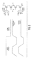
- FIG. 2 shows exemplary waveforms for the clock signal CLK and a gating signal ("Gating Enable") along with an example of a circuit arrangement that may be employed to generate such waveforms.
- the circuit arrangement comprises an AND logic gate 24 having the clock signal CLK provided to its first input and having a delayed and inverted version of the clock signal CLK provided to its second input.
- the output of the AND logic gate 24 is provided to the first input of a Multiplexer MUX 26, which has a supply voltage VDD provided to its second input and the MODE signal provided to its control input.
- the value of the supply voltage VDD or the AND logic gate output is provided at the output of the multiplexer MUX 26 as the gating signal ("Gating Enable").
- a simulation model has been used to verify the concept of the proposed GRVCO-based ADC.
- the GRVCO-based ADC is assumed to have about 76dB SQNR at 100MS/s.
- the former case (i) may initially appear to be better than the latter case (ii), this is not necessarily true because more SQNR enhancement is not necessary once enough SQNR is obtained. Furthermore, the latter cases' power consumption in the VCO is halved due to the doubled sampling period.
- T ACTIVE T GRVCO ⁇ M + T REMAINDER
- E DELAY unit delay element's switching energy consumption
- T DELAY unit delay element's propagation delay
- E TFF T flip-flop's energy consumption
- E DFF D flip-flops' energy consumption
- M is an integer.
- a coarse quantizer and a fine quantizer mainly comprises T flip-flops and D flip-flops, respectively. An encoder's energy consumption is neglected.
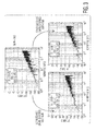
- Figure 5A is a graph of power versus sampling frequency for a conventional VCO-based ADC.
- Figure 5B is a graph of power versus sampling frequency for a GRVCO-based ADC according to an embodiment. It will therefore be appreciated that Figure 5 enables a comparison of power scalability between a conventional VCO-based ADC and a GRVCO-based ADC according to an embodiment. Although the specific numbers in the plots can change, depending on actual implementations, improved power scalability is observed in the GRVCO mode. Thus, the proposed GRVCO-based ADC demonstrates improved power scalability with constant bit resolution performance, and this is illustrated by Figure 5 .
- Digital calibration can be used instead of an analog feedback loop in order to save area and power consumption.
- a look-up table can be used for the nonlinearity characterization and distortion correction.
- near-worst corner design can be used.
- Forward Body Bias (FBB)/Reverse Body Bias (RBB) may be used to tune the circuit after fabrication.
- the noise shaping property may be important in a VCO-based ADC in order to improve the resolution performance.
- an analog state at each delay element's output may be preserved when the oscillation is stopped.
- Figure 6 shows the output behaviour of a conventional GVCO and a GRVCO according to an embodiment.
- Figure 8 (at the right-hand side) is an example of a delay cell implementation in a GRVCO according to an embodiment.
- the proposed GRVCO preserves the oscillation state/phase when oscillation is suspended (e.g. when gating is enabled).
- This analogue state preservation of the proposed GRVCO enables first-order noise shaping, leading to the resolution enhancement.
- a VCO-based ADC has some architectural variants, such as a differential architecture and a time-interleaved architecture.
- a differential architecture using two VCOs is known to improve linearity by cancelling even-order distortion.
- a time-interleaved architecture is useful for energy efficient high speed applications.
- a GRVCO according to an embodiment may be used to replace a VCO in these variants.
- Figure 7 shows a differential architecture employing first and second GRVCOs according to an embodiment.
- This differential architecture is similar to that shown in Figure 1 , except that it employs a second GRVCO 30 and a second quantizer 32 arranged in a similar manner to the first GRVCO 10 and first quantizer 12.
- the output from each quantizer 12,32 is provided to a summation unit 34 which then has its output provided to the frequency extraction stage 16.
- the first and second GRVCOs each have their own input voltage signal V_in1 and V_in2, respectively, and gating signal generator.
- Figure 8 shows a time-interleaved architecture employing first 40 to fourth 46 GRVCO-based ADCs according to an embodiment, wherein the output of each GRVCO-based ADC is provided to a multiplexer MUX 48.
- step 90 an input voltage is provided to a GRVCO.
- step 92 a phase signal is generated using a GRVCO according to the input voltage.
- the step 402 of generating a phase signal includes operating the GRVCO in either a first or second mode of operation according to a mode control signal, wherein, in the first mode of operation, the GRVCO operates in a VCO mode with gating disabled and, in the second mode of operation, the GRVCO operates in a GRVCO mode wherein gating is enabled or disabled according to a gating signal.
- the gating control signal may be generated according to a clock signal and the mode control signal.
- step 94 a quantised phase output signal is generated based on the generated phase signal.
- step 96 the generated quantised phase output signal is received for processing.
- the method then proceeds to step 98 wherein one or more delayed versions of the received quantised phase output signal are created an output signal is generated based on the one or more delayed versions of the received quantised phase output signal.
- the computer system 100 is configured to implement an ADC conversion method to an embodiment of the invention.
- the system comprises a processing unit 105 having an interface 110, and a non-transitory data storage unit 120 connected to the processing unit 105.
- the interface 110 is configured to receive an input voltage (or a control signal for defining an input voltage).
- the data storage unit 120 is configured to store computer-readable program code for execution by the processing unit 105.
- the processing unit 105 is configured to execute a computer program (defined at least in part by computer-readable program code stored by the data storage unit 120) which, when executed, causes the system to implement the steps of a method according to an embodiment, for example the steps as shown in Figure 9 .
- the processing unit 105 is configured to receive, via the interface 110, an input voltage.
- the processing unit 105 operates a GRVCO to generate a phase signal according the input voltage, and then generates a quantised phase output signal based on the generated phase signal.
- the processing unit 105 also generates one or more delayed versions of the quantised phase output signal. Based on the one or more delayed versions of the quantised phase output signal, the processing unit 105 generates an output signal. The generated output signal is supplied from the processing unit 105 to a user or external application via the interface 110. The processing unit 105 may also supply the generated output signal to the data storage unit 120 (so that the output signal can be stored by the data storage unit 120).
- Embodiments may thus provide an apparatus and method for ADC conversion using a GRVCO. It will be clear to one of ordinary skill in the art that all or part of the method of one embodiment of the present invention may suitably and usefully be embodied in a logic apparatus, or a plurality of logic apparatus, comprising logic elements arranged to perform the steps of the method and that such logic elements may comprise hardware components, firmware components or a combination thereof.
- a logic arrangement may suitably be embodied in a logic apparatus comprising logic elements to perform the steps of the method, and that such logic elements may comprise components such as logic gates in, for example a programmable logic array or application-specific integrated circuit.
- Such a logic arrangement may further be embodied in enabling elements for temporarily or permanently establishing logic structures in such an array or circuit using, for example, a virtual hardware descriptor language, which may be stored and transmitted using fixed or transmittable carrier media.
- one embodiment may be realized in the form of a computer implemented method of deploying a service comprising steps of deploying computer program code operable to cause the computer system to perform all the steps of the method when deployed into a computer infrastructure and executed thereon.
- one embodiment may be realized in the form of a data carrier having functional data thereon, the functional data comprising functional computer data structures to, when loaded into a computer system and operated upon thereby, enable the computer system to perform all the steps of the method.
- each block in the flowchart or block diagrams may represent a module, segment, or portion of code, which comprises one or more executable instructions for implementing the specified logical function(s).
- the functions noted in the block may occur out of the order noted in the figures. For example, two blocks shown in succession may, in fact, be executed substantially concurrently, or the blocks may sometimes be executed in the reverse order, depending upon the functionality involved.
- Embodiments may be used in low power applications demanding multiple operating speeds and multiple standard compliancy.
- a conventional VCO-based ADC can be replaced with a GRVCO-based ADC according to an embodiment.
- a GRVCO can be used for both conventional VCO-based ADC applications and power scalable ADC applications which require wide input bandwidth or low oversampling ratio.
- Such applications where a GRVCO-based ADC according to an embodiment may be employed include a multi-format video processor, software-defined radio, multi-sensor system, etc.
- Embodiments may provide GRVCO for voltage-to-phase conversion, a counter and an encoder for phase-to-digital conversion.
- a method is generally conceived to be a self-consistent sequence of steps leading to a desired result. These steps require physical manipulations of physical quantities. Usually, though not necessarily, these quantities take the form of electrical or magnetic signals capable of being stored, transferred, combined, compared, and otherwise manipulated. It is convenient at times, principally for reasons of common usage, to refer to these signals as bits, values, parameters, items, elements, objects, symbols, characters, terms, numbers, or the like. It should be noted, however, that all of these terms and similar terms are to be associated with the appropriate physical quantities and are merely convenient labels applied to these quantities
- the present invention may further suitably be embodied as a computer program product for use with a computer system.
- Such an implementation may comprise a series of computer-readable instructions either fixed on a tangible medium, such as a computer readable medium, for example, e.g. a CD-ROM, DVD, USB stick, memory card, network-area storage device, internet-accessible data repository, and so on, or transmittable to a computer system, via a modem or other interface device, over either a tangible medium, including but not limited to optical or analogue communications lines, or intangibly using wireless techniques, including but not limited to microwave, infrared or other transmission techniques.
- the series of computer readable instructions embodies all or part of the functionality previously described herein. Embodiments may include the features recited in the following numbered clauses:
- Such computer readable instructions can be written in a number of programming languages for use with many computer architectures or operating systems. Further, such instructions may be stored using any memory technology, present or future, including but not limited to, semiconductor, magnetic, or optical, or transmitted using any communications technology, present or future, including but not limited to optical, infrared, or microwave. It is contemplated that such a computer program product may be distributed as a removable medium with accompanying printed or electronic documentation, for example, shrink-wrapped software, pre-loaded with a computer system, for example, on a system ROM or fixed disk, or distributed from a server or electronic bulletin board over a network, for example, the Internet or World Wide Web.
- an Analogue to Digital Converter having a Gated Ring Voltage Controlled Oscillator, GRVCO, to generate a phase signal according to an input voltage; and a quantization circuit to generate a quantized phase output signal according.
- the GRVCO operates in either a first or second mode of operation according to a gating control signal. In the first mode of operation, the GRVCO operates in a VCO mode with gating disabled. In the second mode of operation, the GRVCO operates in a GRVCO mode wherein gating is enabled or disabled according to a gating signal.
Landscapes
- Engineering & Computer Science (AREA)
- Theoretical Computer Science (AREA)
- Analogue/Digital Conversion (AREA)
- Stabilization Of Oscillater, Synchronisation, Frequency Synthesizers (AREA)
Applications Claiming Priority (1)
| Application Number | Priority Date | Filing Date | Title |
|---|---|---|---|
| US13/780,679 US8988264B2 (en) | 2013-02-28 | 2013-02-28 | Analogue to digital converter |
Publications (2)
| Publication Number | Publication Date |
|---|---|
| EP2773046A2 true EP2773046A2 (de) | 2014-09-03 |
| EP2773046A3 EP2773046A3 (de) | 2015-05-20 |
Family
ID=50137544
Family Applications (1)
| Application Number | Title | Priority Date | Filing Date |
|---|---|---|---|
| EP20140156003 Ceased EP2773046A3 (de) | 2013-02-28 | 2014-02-20 | Analog-Digital-Wandler |
Country Status (3)
| Country | Link |
|---|---|
| US (1) | US8988264B2 (de) |
| EP (1) | EP2773046A3 (de) |
| CN (1) | CN104022780B (de) |
Cited By (3)
| Publication number | Priority date | Publication date | Assignee | Title |
|---|---|---|---|---|
| GB2541079A (en) * | 2013-06-26 | 2017-02-08 | Cirrus Logic Int Semiconductor Ltd | Analog-to-digital converter |
| EP3410603A1 (de) * | 2017-05-30 | 2018-12-05 | Infineon Technologies Austria AG | System und verfahren für einen überabgetasteten datenwandler |
| EP3403328A4 (de) * | 2016-01-15 | 2019-08-28 | Seamless Microsystems, Inc. | Systeme und verfahren für auf ringoszillator basierende operationsverstärker für skalierte cmos-technologien |
Families Citing this family (7)
| Publication number | Priority date | Publication date | Assignee | Title |
|---|---|---|---|---|
| JP6032082B2 (ja) * | 2013-03-25 | 2016-11-24 | 富士通株式会社 | 受信回路及び半導体集積回路 |
| US9647827B1 (en) * | 2015-10-23 | 2017-05-09 | Raytheon Company | Precision clock enabled time-interleaved data conversion |
| CN105406867B (zh) * | 2015-12-17 | 2018-11-06 | 成都博思微科技有限公司 | 一种时间交织流水线adc系统及其时序操作方法 |
| US9900538B2 (en) | 2016-05-18 | 2018-02-20 | Semiconductor Components Industries, Llc | Phase delay counting analog-to-digital converter circuitry |
| US10734977B1 (en) * | 2019-04-10 | 2020-08-04 | Silicon Laboratories Inc. | Efficient voltage controlled oscillator (VCO) analog-to-digital converter (ADC) |
| US10826514B1 (en) * | 2019-10-15 | 2020-11-03 | Ciena Corporation | Noise-shaping enhanced gated ring oscillator based analog-to-digital converters |
| US12483264B2 (en) * | 2023-06-12 | 2025-11-25 | The Regents Of The University Of Michigan | Analog-to-digital converter with 3rd order noise transfer function |
Family Cites Families (4)
| Publication number | Priority date | Publication date | Assignee | Title |
|---|---|---|---|---|
| US7609187B2 (en) * | 2005-02-10 | 2009-10-27 | National University Corporation Nagoya University | ΔΣ modulator and ΔΣ analog-digital converter |
| US8471743B2 (en) * | 2010-11-04 | 2013-06-25 | Mediatek Inc. | Quantization circuit having VCO-based quantizer compensated in phase domain and related quantization method and continuous-time delta-sigma analog-to-digital converter |
| US8542138B2 (en) * | 2011-01-28 | 2013-09-24 | The Regents Of The University Of California | Ring oscillator delta sigma ADC modulator with replica path nonlinearity calibration |
| JP2012244199A (ja) * | 2011-05-14 | 2012-12-10 | Handotai Rikougaku Kenkyu Center:Kk | オペアンプレス・キャパシタレスad変換器およびtd変換器 |
-
2013
- 2013-02-28 US US13/780,679 patent/US8988264B2/en active Active
-
2014
- 2014-02-20 EP EP20140156003 patent/EP2773046A3/de not_active Ceased
- 2014-02-25 CN CN201410064729.5A patent/CN104022780B/zh active Active
Non-Patent Citations (3)
| Title |
|---|
| KIM YONGTAE ET AL: "A 0.38 V near/sub-digitally controlled low-dropout regulator with enhanced power supply noise rejection in 90 nm CMOS process", IET CIRCUITS DEVICES AND SYSTEMS, THE INSTITUTION OF ENGINEERING AND TECHNOLOGY, GB, vol. 7, no. 1, 1 January 2013 (2013-01-01), pages 31 - 41, XP006044676, ISSN: 1751-858X, DOI: 10.1049/IET-CDS.2012.0114 * |
| WONSIK YU ET AL: "A Time-Domain High-Order MASH $\Delta\Sigma$ ADC Using Voltage-Controlled Gated-Ring Oscillator", IEEE TRANSACTIONS ON CIRCUITS AND SYSTEMS I: REGULAR PAPERS, IEEE, US, vol. 60, no. 4, 13 August 2012 (2012-08-13), pages 856 - 866, XP011498536, ISSN: 1549-8328, DOI: 10.1109/TCSI.2012.2209298 * |
| YU MINGYAN ET AL: "A temperature stabilized multi-path gated ring oscillator based TDC", COMPUTER SCIENCE AND INFORMATION PROCESSING (CSIP), 2012 INTERNATIONAL CONFERENCE ON, IEEE, 24 August 2012 (2012-08-24), pages 703 - 708, XP032241116, ISBN: 978-1-4673-1410-7, DOI: 10.1109/CSIP.2012.6308951 * |
Cited By (10)
| Publication number | Priority date | Publication date | Assignee | Title |
|---|---|---|---|---|
| GB2541079A (en) * | 2013-06-26 | 2017-02-08 | Cirrus Logic Int Semiconductor Ltd | Analog-to-digital converter |
| GB2515526B (en) * | 2013-06-26 | 2017-11-08 | Cirrus Logic Int Semiconductor Ltd | Analog-to-digital convertor |
| GB2541079B (en) * | 2013-06-26 | 2018-03-14 | Cirrus Logic Int Semiconductor Ltd | Analog-to-digital converter |
| EP3403328A4 (de) * | 2016-01-15 | 2019-08-28 | Seamless Microsystems, Inc. | Systeme und verfahren für auf ringoszillator basierende operationsverstärker für skalierte cmos-technologien |
| US10483916B2 (en) | 2016-01-15 | 2019-11-19 | Seamless Microsystems, Inc. | Systems and methods for ring-oscillator based operational amplifiers for scaled CMOS technologies |
| EP3410603A1 (de) * | 2017-05-30 | 2018-12-05 | Infineon Technologies Austria AG | System und verfahren für einen überabgetasteten datenwandler |
| KR20180131419A (ko) * | 2017-05-30 | 2018-12-10 | 인피니언 테크놀로지스 오스트리아 아게 | 오버샘플링된 데이터 변환기용 시스템 및 방법 |
| CN108988864A (zh) * | 2017-05-30 | 2018-12-11 | 英飞凌科技奥地利有限公司 | 用于过采样数据转换器的系统和方法 |
| US10447294B2 (en) | 2017-05-30 | 2019-10-15 | Infineon Technologies Austria Ag | System and method for an oversampled data converter |
| CN108988864B (zh) * | 2017-05-30 | 2024-03-26 | 英飞凌科技奥地利有限公司 | 用于过采样数据转换器的系统和方法 |
Also Published As
| Publication number | Publication date |
|---|---|
| US20140240157A1 (en) | 2014-08-28 |
| CN104022780A (zh) | 2014-09-03 |
| EP2773046A3 (de) | 2015-05-20 |
| CN104022780B (zh) | 2016-09-14 |
| US8988264B2 (en) | 2015-03-24 |
Similar Documents
| Publication | Publication Date | Title |
|---|---|---|
| US8988264B2 (en) | Analogue to digital converter | |
| US9479190B2 (en) | Successive approximation register-based analog-to-digital converter with increased time frame for digital-to-analog capacitor settling | |
| US10303124B2 (en) | Time-to-digital converter | |
| US8198921B2 (en) | Dynamic comparator with background offset calibration | |
| CN109314521B (zh) | 用于时间交错式逐次逼近模数转换器的异步时钟生成 | |
| US7696910B2 (en) | Dither circuit and analog digital converter having dither circuit | |
| US7629916B2 (en) | Multiple output time-to-digital converter | |
| JP5749372B2 (ja) | アナログディザリングを用いる時間/デジタル変換 | |
| EP2107683A1 (de) | Analog-Digital-Wandler mit komparatorbasierter asynchroner binärer Suche | |
| US9250612B2 (en) | System and method for a time-to-digital converter | |
| US10778239B2 (en) | Electronic circuit for implementing modulator configured to perform noise shaping in digital domain | |
| CN106341134B (zh) | 具有局部交错和重采样的数模转换器 | |
| KR102029551B1 (ko) | 낸드-게이트 링 발진기 시간 증폭기를 활용한 2단 시간-디지털 변환기 | |
| CN110235372B (zh) | 一种具有降低回扫噪声的双倍数据速率时间内插量化器 | |
| Yang et al. | An 8-bit 2.8 GS/s Flash ADC with Time-based Offset Calibration and Interpolation in 65 nm CMOS | |
| US20170322520A1 (en) | Time register | |
| EP3568918A1 (de) | Interpolierender analog-digital-wandler mit doppelter datenrate | |
| US12107596B2 (en) | Successive approximation register based time-to-digital converter using a time difference amplifier | |
| JP5129298B2 (ja) | DWA(Data−Weighted−Averaging)回路、それを用いたデルタシグマ変調器 | |
| CN114884492B (zh) | 一种应用于模数转换器的基于Gm-CCO型的比较器电路 | |
| Park et al. | Low-power all-digital ΔΣ TDC with bi-directional gated delay line time integrator | |
| KR101601785B1 (ko) | 시간 디지털 변환기 및 그를 이용한 변환 방법 | |
| Abdelaziz et al. | A time latch for high speed time‐based ADCs | |
| KR101725833B1 (ko) | 10비트 축차 비교형 아날로그 디지털 변환기 | |
| Kim et al. | A nonuniform quantization scheme for high speed SAR ADC architecture |
Legal Events
| Date | Code | Title | Description |
|---|---|---|---|
| PUAI | Public reference made under article 153(3) epc to a published international application that has entered the european phase |
Free format text: ORIGINAL CODE: 0009012 |
|
| 17P | Request for examination filed |
Effective date: 20140326 |
|
| AK | Designated contracting states |
Kind code of ref document: A2 Designated state(s): AL AT BE BG CH CY CZ DE DK EE ES FI FR GB GR HR HU IE IS IT LI LT LU LV MC MK MT NL NO PL PT RO RS SE SI SK SM TR |
|
| AX | Request for extension of the european patent |
Extension state: BA ME |
|
| PUAL | Search report despatched |
Free format text: ORIGINAL CODE: 0009013 |
|
| AK | Designated contracting states |
Kind code of ref document: A3 Designated state(s): AL AT BE BG CH CY CZ DE DK EE ES FI FR GB GR HR HU IE IS IT LI LT LU LV MC MK MT NL NO PL PT RO RS SE SI SK SM TR |
|
| AX | Request for extension of the european patent |
Extension state: BA ME |
|
| RIC1 | Information provided on ipc code assigned before grant |
Ipc: H03M 1/06 20060101ALN20150416BHEP Ipc: H03M 1/12 20060101ALN20150416BHEP Ipc: H03M 1/60 20060101AFI20150416BHEP |
|
| RBV | Designated contracting states (corrected) |
Designated state(s): AL AT BE BG CH CY CZ DE DK EE ES FI FR GB GR HR HU IE IS IT LI LT LU LV MC MK MT NL NO PL PT RO RS SE SI SK SM TR |
|
| 17Q | First examination report despatched |
Effective date: 20160406 |
|
| STAA | Information on the status of an ep patent application or granted ep patent |
Free format text: STATUS: THE APPLICATION HAS BEEN REFUSED |
|
| 18R | Application refused |
Effective date: 20171109 |