US7696910B2 - Dither circuit and analog digital converter having dither circuit - Google Patents
Dither circuit and analog digital converter having dither circuit Download PDFInfo
- Publication number
- US7696910B2 US7696910B2 US12/073,087 US7308708A US7696910B2 US 7696910 B2 US7696910 B2 US 7696910B2 US 7308708 A US7308708 A US 7308708A US 7696910 B2 US7696910 B2 US 7696910B2
- Authority
- US
- United States
- Prior art keywords
- dither
- pairs
- circuit
- input
- complementary signal
- Prior art date
- Legal status (The legal status is an assumption and is not a legal conclusion. Google has not performed a legal analysis and makes no representation as to the accuracy of the status listed.)
- Expired - Fee Related
Links
Images


Classifications
-
- H—ELECTRICITY
- H03—ELECTRONIC CIRCUITRY
- H03M—CODING; DECODING; CODE CONVERSION IN GENERAL
- H03M3/00—Conversion of analogue values to or from differential modulation
- H03M3/30—Delta-sigma modulation
- H03M3/322—Continuously compensating for, or preventing, undesired influence of physical parameters
- H03M3/324—Continuously compensating for, or preventing, undesired influence of physical parameters characterised by means or methods for compensating or preventing more than one type of error at a time, e.g. by synchronisation or using a ratiometric arrangement
- H03M3/326—Continuously compensating for, or preventing, undesired influence of physical parameters characterised by means or methods for compensating or preventing more than one type of error at a time, e.g. by synchronisation or using a ratiometric arrangement by averaging out the errors
- H03M3/328—Continuously compensating for, or preventing, undesired influence of physical parameters characterised by means or methods for compensating or preventing more than one type of error at a time, e.g. by synchronisation or using a ratiometric arrangement by averaging out the errors using dither
-
- H—ELECTRICITY
- H03—ELECTRONIC CIRCUITRY
- H03K—PULSE TECHNIQUE
- H03K3/00—Circuits for generating electric pulses; Monostable, bistable or multistable circuits
- H03K3/84—Generating pulses having a predetermined statistical distribution of a parameter, e.g. random pulse generators
-
- H—ELECTRICITY
- H03—ELECTRONIC CIRCUITRY
- H03M—CODING; DECODING; CODE CONVERSION IN GENERAL
- H03M3/00—Conversion of analogue values to or from differential modulation
- H03M3/30—Delta-sigma modulation
- H03M3/39—Structural details of delta-sigma modulators, e.g. incremental delta-sigma modulators
- H03M3/436—Structural details of delta-sigma modulators, e.g. incremental delta-sigma modulators characterised by the order of the loop filter, e.g. error feedback type
- H03M3/456—Structural details of delta-sigma modulators, e.g. incremental delta-sigma modulators characterised by the order of the loop filter, e.g. error feedback type the modulator having a first order loop filter in the feedforward path
Definitions
- the present invention relates to a dither circuit for a quantizer, and more particularly, to a dither circuit correcting quantization error generated in an analog digital converter (ADC).
- ADC analog digital converter
- FIG. 6 is a configuration diagram of a first-order ⁇ (delta sigma) ADC without dither signal. This first-order ⁇ ADC functions as follows.
- a sampling clock ck When a sampling clock ck is in active state, switches SWain and SWsam are closed and charges sampling analog input signal Vain are stored in an input capacitor C 1 .
- switches SWain and SWsam are closed and charges sampling analog input signal Vain are stored in an input capacitor C 1 .
- switches SWdac and SWint are closed, and charges are transmitted to an integral capacitor C 2 according to a feedback reference signal Vr.
- integration is performed in the C 2 to change an integrator output Vout.
- the integrator output Vout is input to a comparator 3 which functions as a quantizer.
- a quantization output PDM which is the output from the comparator 3 , is delayed by one clock cycle by a delay device 4 and is input to a 1-bit digital analog converter (DAC) 6 .
- the DAC 6 outputs a feedback reference signal Vr.
- the level of the feedback reference signal Vr has two values of Vrp and Vrn, and the level is determined to be Vrp or Vrn according
- a decimation filter 5 obtains the quantization output PDM and removes high side out-of-band noise that is shaped by a delta sigma modulator 10 . Then the decimation filter 5 thins out and changes the data output rate to a desired one to output the digital signal output Dout.
- FIG. 7 shows output characteristics of the ⁇ type ADC when an analog input signal is in the vicinity of zero.
- the digital output signal outputs constant value. This is because some loss is caused in the integrator. The loss is caused mainly because gain of an operational amplifier forming the integrator has limit, leak current is generated in the capacitor or the switch, or the integrator is not in an ideal state due to existence of parasitic element and soon. Due to this loss, the feedback reference signal is in a stationary state where the feedback reference signal repeats positive side and negative side when the analog input signal is in the vicinity of zero, and the digital output signal has constant value. Therefore, as shown in FIG. 8 , the error is also increased when the analog input signal is in the vicinity of zero.
- the stationary state where the feedback reference signal repeats positive side and negative side is needed to be avoided when the analog input signal is in the vicinity of zero.
- the process for adding the dither signals is typically used to achieve this object.
- FIG. 9 shows a configuration of the ⁇ type ADC disclosed in Japanese Unexamined Patent Application Publication No. 2002-100992.
- the ⁇ type ADC includes a dither circuit 1 , a switched capacitor type integrator 2 , a quantizer 3 made of a comparator, a delay device 4 made of a flip-flop, a decimation filter 5 , and a 1-bit DAC 6 .
- FIG. 10 shows configurations of the dither circuit 1 of the ⁇ type ADC and the 1-bit DAC shown in FIG. 9 , and switched capacitors transmitting charges proportional to signal potentials generated at the dither circuit and the 1-bit DAC to an integral capacitor of the integrator 2 .
- the 1-bit DAC 6 includes a switching device 31 controlled by an output Sd of the delay device 4 .
- the dither circuit 1 includes a switching device 37 controlled by signal obtained by dividing the frequency of sampling clock fs by n using a frequency divider.
- the frequency dividing ratio of the frequency divider is set so that the cycle of the dither signals becomes more than 1 ⁇ 8 of the output cycle of the decimation filter 5 .
- the switching device 37 switches reference voltages V 2 and V 3 generated at the resistors 39 to 43 that are connected in series to output the square wave dither whose amplitude is V 2 -V 3 .
- a switched capacitor circuit includes switches 32 and 34 that function at a first timing, switches 35 and 36 that function at a second timing, and a capacitor 33 .
- FIG. 11 shows a configuration of the ADC of U.S. Pat. No. 5,940,138
- FIG. 12 shows the dither waveform thereof.
- the dither is generated from the square wave having frequencies of 1 ⁇ 2 and 1 ⁇ 4 of the sampling clock CLK obtained by dividing frequency of the sampling clock CLK using flip-flops 803 B and 803 C.
- the two square waves having frequencies of 1 ⁇ 2 and 1 ⁇ 4 are added to the analog video input signal DATA output from a buffer amplifier 805 as the dither of the amplitude of 1 ⁇ 2 LSB P-P and 1 ⁇ 4 LSB P-P by an adding device which includes weighted resistors R, 512 R, and 1024 R.
- exclusive OR operation is performed on the signal obtained by dividing frequency of horizontal synchronizing signal H by 2 and the square wave having frequency of 1 ⁇ 2 of the sampling clock CLK at EX-OR 804 A.
- Exclusive OR operation is also performed on the signal obtained by dividing frequency of horizontal synchronizing signal H by 2 and the square wave having frequency of 1 ⁇ 4 of the sampling clock CLK at EX-OR 804 B. After these exclusive OR operations, these signals are added to the adding device. Therefore, the ADC has a configuration where the polarity of the dither is inverted for each one horizontal line.
- the resistor that is 512 times or 1024 times larger than the resistor for analog signal input is needed to determine the amplitude of the dither, which increases the circuit size.
- the dither amplitude is 1/512 or 1/1024 of the analog signal input range, the phenomena where the digital output signal becomes constant when the analog input signal Vain is in the vicinity of zero cannot be improved.
- a dither circuit includes a dither generating circuit generating a plurality of complementary signal pairs, and a dither input circuit generating a plurality of dither signals from the plurality of complementary signal pairs to add the generated dither signals to an analog input signal, in which the plurality of complementary signal pairs have different frequencies with each other, the dither input circuit includes capacitors provided for each of the plurality of complementary signal pairs and a plurality of switch pairs including first and second switches having one terminals connected to each one terminal of the capacitors, and the other terminals of the capacitors are connected to an adding point to the analog input signal, the first switch supplies ones of the complementary signal pairs to one terminals of the capacitors when a clock signal is in effective state, and the second switch supplies the others of the complementary signal pairs to one terminals of the capacitors when an inverting clock signal of the clock signal is in effective state.
- the dither generating circuit of the present invention generates a plurality of square waves having different frequencies. Therefore, it is possible to form the dither generating circuit only by the frequency divider and therefore to suppress the increase of the circuit size.
- the dither input circuit of the present invention can be formed by switches and a plurality of capacitors that are smaller than the capacitor for analog signal input, which makes it possible to suppress the increase of the circuit size. According to the dither circuit of the present invention to which these circuits are applied, it is possible to suppress the increase of the circuit size to improve the AD conversion characteristics when the analog input signal Vain is in the vicinity of zero and when another analog signal is input.
- FIG. 1 shows a configuration of a ⁇ ADC to which a dither circuit according to the present invention is added
- FIG. 2 shows a configuration of a dither generating circuit in the dither circuit according to the present invention
- FIG. 3 shows a configuration of the dither circuit according to one embodiment of the present invention
- FIG. 4A shows dither patterns according to one embodiment of the present invention
- FIG. 4B shows dither patterns according to one embodiment of the present invention
- FIG. 4C shows dither patterns according to one embodiment of the present invention
- FIG. 4D shows dither patterns according to one embodiment of the present invention
- FIG. 5 shows input versus error characteristics of the ⁇ ADC to which the dither circuit according to the present invention is added
- FIG. 6 shows a configuration of the ⁇ ADC without dither signal
- FIG. 7 shows output characteristics when an analog input signal of the ⁇ ADC in FIG. 6 is in the vicinity of zero
- FIG. 8 shows input versus error characteristics of the ⁇ ADC in FIG. 6 ;
- FIG. 9 shows a configuration of a conventional ⁇ ADC using a single square wave dither signal
- FIG. 10 shows configurations of the dither circuit of the ⁇ type ADC and a 1-bit DAC shown in FIG. 9 , and switched capacitors transmitting charges proportional to signal potentials generated at the dither circuit and the 1-bit DAC to an integral capacitor of an integrator;
- FIG. 11 shows a configuration of the conventional ADC using two square wave dither signals
- FIG. 12 shows a dither pattern of the conventional ADC shown in FIG. 11 ;
- FIG. 13 shows input versus error characteristics of the conventional ADC using the single square wave dither signal.
- FIG. 1 shows a configuration of one embodiment of the present invention.
- a dither circuit including a dither generating circuit 15 and a dither input circuit 20 is added to a ⁇ type ADC which is the same as shown in FIG. 6 .
- the dither circuit according to the present invention includes the dither generating circuit 15 and the dither input circuit 20 .
- the dither generating circuit 15 divides frequency of clock signal ck and generates a plurality of complementary signal pairs (Vd 1 , Vd 1 b ), (Vd 2 , Vd 2 b ), . . .
- Vdj, Vdjb having frequencies of 1 ⁇ 2 n (n is an integer of one or more than one) of the clock signal ck. Then the dither generating circuit 15 supplies the generated signal pairs to the dither input circuit 20 .
- the plurality of complementary signal pairs (Vd 1 , Vd 1 b ), (Vd 2 , Vd 2 b ), . . . (Vdj, Vdjb) each have different frequencies.
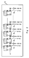
- FIG. 2 shows an example of a configuration of the dither generating circuit 15 .
- the dither generating circuit 15 has m (m is an integer of two or more than two) 1 ⁇ 2 frequency dividing circuits ( 501 , 502 , 503 , 504 , . . . 50 m ) that are made of D-type flip-flops and inverters connected in series.
- M 1 ⁇ 2 frequency dividing circuits generate complementary signal pairs (Vdiv 2 , Vdiv 2 b ), (Vdiv 4 , Vdiv 4 b ), (Vdiv 8 , Vdiv 8 b ), (Vdiv 16 , Vdiv 16 b ), . . .
- VdivX, VdivXb having amplitude between power source potential VDD and ground potential GND.
- j (j is an integer of two or more than two) complementary signal pairs (Vd 1 , Vd 1 b ), (Vd 2 , Vd 2 b ), . . . (Vdj, Vdjb) are selected from among m complementary signal pairs and the selected pairs are supplied to the dither input circuit 20 .
- the dither input circuit 20 includes capacitors Cd 1 , Cd 2 , . . . Cdj, each being provided corresponding to the plurality of complementary signal pairs (Vd 1 , Vd 1 b ), (Vd 2 , Vd 2 b ), . . . (Vdj, Vdjb).
- One ends of the capacitors Cd 1 , Cd 2 , . . . Cdj are connected to one ends of the switches forming the switch pairs (Swd 1 , Swd 1 b ), (Swd 2 , Swd 2 b ), . . . (Swdj, Swdjb), respectively.
- the complementary signal pairs (Vd 1 , Vd 1 b ), (Vd 2 , Vd 2 b ), . . . (Vdj, Vdjb) are supplied to each of the other ends of the switches forming the switch pairs (Swd 1 , Swd 1 b ), (Swd 2 , Swd 2 b ), . . . (Swdj, Swdjb).
- Each of the other ends of the capacitors Cd 1 , Cd 2 , . . . Cdj are connected to an adding point A which is an input of an integrator.
- switches Swd 1 , Swd 2 , . . . Swdj of each switch pair are controlled to be closed when the clock signal ck is in active state and controlled to be opened when inverting clock signal ckb is in active state.
- the other switches Swd 1 b , Swd 2 b , . . . Swdjb are controlled to be closed when the inverting clock signal ckb is in active state and controlled to be opened when the clock signal ck is in active state.
- the signals Vd 1 , Vd 2 , . . . Vdj are supplied to each capacitor of the dither input circuit of the present invention in a former part of 1 sampling clock cycle of the ⁇ type ADC, whereas the inverting signals Vd 1 b , Vd 2 b , . . . Vdjb are supplied to each capacitor of the dither input circuit in a latter part of 1 sampling clock cycle.
- the first-order ⁇ ADC to which the dither circuit of FIG. 1 is added behaves as follows.
- the sampling clock ck is in active state, switches SWain and SWsam are closed and charges sampling analog input signal Vain are stored in an input capacitor C 1 .
- the adding point A has ground potential and the charges according to the signals Vd 1 , Vd 2 , . . . Vdj are stored in the capacitors Cd 1 , Cd 2 , . . . Cdj, respectively.
- Vd 1 b , Vd 2 b , . . . Vdjb are the inverting signals of Vd 1 , Vd 2 , . . . Vdj, respectively. Therefore, the charges transmitted to the integral capacitor C 2 from the capacitors Cd 1 , Cd 2 , . . . Cdj are twice as much as the charges first stored in the Cd 1 , Cd 2 , . . . Cdj. In other words, it is possible to decrease the capacitance values of the Cd 1 , Cd 2 , . . . Cdj and to suppress the increase in the area. For example, the capacitance values of the Cd 1 , Cd 2 , . . . Cdj can be less than 1/10 of the capacitor for the analog signal input C 1 .
- signals output from the dither generating circuit 15 have amplitude between the power source potential VDD and the ground potential GND. Therefore, it is possible for the MOS transistor forming the switches Swd 1 , Swd 2 , . . . Swdj and the switches Swd 1 b , Swd 2 b , . . . Swdjb to have enough VGS-VTH. Moreover, the values of the capacitors Cd 1 , Cd 2 , . . . Cdj are so small that time constant obtained by the capacitors Cd 1 , Cd 2 , . . . Cdj and ON resistances of the switches are not changed or can be made small even if ON resistances of those switches are increased. Therefore, it is possible to use transistor which is smaller than the switch inside the ⁇ modulator so as to further suppress the increase in the area.
- the lowest frequency needs to be the frequency that can be removed by the decimation filter 5 .
- FIG. 3 shows a configuration of the dither circuit of the embodiment of the present invention.
- FIGS. 4A to 4D each shows a dither pattern of the embodiment.
- the dither pattern is generated by the dither generating circuit 15 and the dither input circuit 20 .
- the dither generating circuit 15 is made only of the 1 ⁇ 2 frequency dividing circuit and the inverter.
- the dither input circuit 20 is made of three switch pairs (Swd 1 , Swd 1 b ), (Swd 2 , Swd 2 b ), (Swd 3 , Swd 3 b ) and three capacitors Cd 1 , Cd 2 , Cd 3 .
- the dither generating circuit 15 outputs the complementary signal pairs (Vd 1 , Vd 1 b ), (Vd 2 , Vd 2 b ), (Vd 3 , Vd 3 b ) having square wave of the frequencies of 1/128, 1/512, and 1/2048 of the sampling clock ck to the dither input circuit 20 .
- the complementary signal pairs (Vdiv 128 , Vdiv 128 b ) having the frequency of 1/128 of the sampling clock ck is added to the capacitor Cd 1 through the switch pair (Swd 1 , Swd 1 b ), the complementary signal pairs (Vdiv 512 , Vdiv 512 b ) having the frequency of 1/512 is added to the capacitor Cd 2 through the switch pairs (Swd 2 , Swd 2 b ), and the complementary signal pairs (Vdiv 2048 , Vdiv 2048 b ) having the frequency of 1/2048 is added to the capacitor Cd 3 through the switch pair (Swd 3 , Swd 3 b ).
- the capacitance values of three capacitors Cd 1 , Cd 2 , and Cd 3 are equal to 1/16, 1/64, and 1/128 of the capacitor for analog signal input C 1 , respectively.
- the dither signals Vd output from the dither input circuit 20 are added to the adding point A of the ⁇ modulator 10 having the same configuration as that shown in FIG. 1 .
- a selector can also be provided. The selector selects the complementary signal pairs having the frequencies of 1/128, 1/512, and 1/2048 of the sampling clock ck from among the plurality of complementary signal pairs generated from the dither generating circuit 15 and supplies the selected pairs to the dither input circuit 20 .
- FIG. 5 shows input versus error characteristics of the ⁇ ADC to which the present embodiment is applied. It can be seen from FIG. 5 that the ⁇ ADC indicates good input versus error characteristics.
Abstract
Description
Claims (15)
Applications Claiming Priority (2)
| Application Number | Priority Date | Filing Date | Title |
|---|---|---|---|
| JP2007091124A JP4763644B2 (en) | 2007-03-30 | 2007-03-30 | Dither circuit and analog-to-digital converter with dither circuit |
| JP2007-091124 | 2007-03-30 |
Publications (2)
| Publication Number | Publication Date |
|---|---|
| US20080238743A1 US20080238743A1 (en) | 2008-10-02 |
| US7696910B2 true US7696910B2 (en) | 2010-04-13 |
Family
ID=39793364
Family Applications (1)
| Application Number | Title | Priority Date | Filing Date |
|---|---|---|---|
| US12/073,087 Expired - Fee Related US7696910B2 (en) | 2007-03-30 | 2008-02-29 | Dither circuit and analog digital converter having dither circuit |
Country Status (3)
| Country | Link |
|---|---|
| US (1) | US7696910B2 (en) |
| JP (1) | JP4763644B2 (en) |
| CN (1) | CN101277111A (en) |
Cited By (9)
| Publication number | Priority date | Publication date | Assignee | Title |
|---|---|---|---|---|
| US20110148676A1 (en) * | 2007-06-22 | 2011-06-23 | Texas Instruments Incorporated | Digital phase locked loop with dithering |
| US8519878B2 (en) * | 2011-06-27 | 2013-08-27 | Broadcom Corporation | Multi-mode analog-to-digital converter |
| US20140132430A1 (en) * | 2012-04-20 | 2014-05-15 | Linear Technology Corporation | Analog-to-digital converter system and method |
| US20140176357A1 (en) * | 2011-04-16 | 2014-06-26 | Abb Technology Ag | Arrangement for reading out an analog voltage signal |
| US9157948B2 (en) | 2012-07-05 | 2015-10-13 | Renesas Electronics Corporation | Semiconductor device and fault diagnosis system |
| US9998275B1 (en) * | 2015-02-20 | 2018-06-12 | Altera Corporation | Digital monobit dithering circuit |
| US10116322B1 (en) * | 2017-12-01 | 2018-10-30 | Raytheon Company | Rail adaptive dither |
| US10700693B2 (en) | 2018-06-19 | 2020-06-30 | Renesas Electronics Corporation | Analog-digital converter, semiconductor device, and voltage signal generation method |
| TWI703830B (en) * | 2019-04-30 | 2020-09-01 | 瑞昱半導體股份有限公司 | Analog to digital converting device and capacitor adjusting method thereof |
Families Citing this family (21)
| Publication number | Priority date | Publication date | Assignee | Title |
|---|---|---|---|---|
| JP5258536B2 (en) * | 2008-12-12 | 2013-08-07 | キヤノン株式会社 | Imaging apparatus and imaging system |
| WO2010095513A1 (en) * | 2009-02-20 | 2010-08-26 | アルプス電気株式会社 | Proximity capacitance detecting circuit and capacitive sensor module |
| JP2010199799A (en) * | 2009-02-24 | 2010-09-09 | Renesas Electronics Corp | Analog/digital conversion circuit |
| JP4944924B2 (en) * | 2009-04-27 | 2012-06-06 | 日本電信電話株式会社 | Signal quantization apparatus, method, program, recording medium thereof, and signal quantization system |
| US8319527B1 (en) * | 2009-04-28 | 2012-11-27 | Linear Technology Corporation | Analog sampler with reduced input current |
| JP5440758B2 (en) * | 2009-05-07 | 2014-03-12 | セイコーエプソン株式会社 | A / D conversion circuit, electronic device, and A / D conversion method |
| TWI390213B (en) | 2009-05-13 | 2013-03-21 | Silicon Motion Inc | Dc voltage measuring apparatus and method for dc voltage measurement |
| CN101900757B (en) * | 2009-05-25 | 2012-10-10 | 慧国(上海)软件科技有限公司 | Method and device for measuring direct current voltage |
| US8174418B2 (en) * | 2009-07-14 | 2012-05-08 | Honeywell International Inc. | Inexpensively improving resolution and reducing noise of low-noise signals |
| US8471741B2 (en) * | 2011-11-14 | 2013-06-25 | Analog Devices, Inc. | Method and device for reducing inter-channel coupling in interleaved and multi-channel ADCs |
| CN103560800B (en) * | 2013-11-04 | 2015-12-02 | 中国电子科技集团公司第四十一研究所 | A kind of jitter generator and shake production method improving ADC+FPGA digital received system sensitivity |
| CN103780228B (en) * | 2014-01-16 | 2016-11-23 | 华为技术有限公司 | A kind of clock jitter improves circuit and method |
| KR20160123708A (en) * | 2015-04-17 | 2016-10-26 | 에스케이하이닉스 주식회사 | Image sensing device |
| US10284400B2 (en) * | 2015-09-01 | 2019-05-07 | Nec Corporation | Delta-sigma modulator, transmitter, and integrator |
| US9748969B1 (en) * | 2016-04-14 | 2017-08-29 | Infineon Technologies Ag | Method of operation for an oversampled data converter |
| US9825645B1 (en) | 2016-12-22 | 2017-11-21 | Infineon Technologies Ag | Self-oscillating dual-slope integrating quantizer for sigma delta modulators |
| US10333543B1 (en) * | 2018-05-10 | 2019-06-25 | Analog Devices Global Unlimited Company | Analog-to-digital converter with noise-shaped dither |
| CN112671405B (en) * | 2020-12-23 | 2023-12-12 | 中国原子能科学研究院 | Ionization chamber charge signal reading device |
| CN112737534B (en) * | 2020-12-23 | 2023-12-12 | 中国原子能科学研究院 | Ionization chamber charge signal reading method |
| US11431939B1 (en) * | 2021-03-30 | 2022-08-30 | Omnivision Technologies, Inc. | Analog to digital converter clock control to extend analog gain and reduce noise |
| CN113515033A (en) * | 2021-04-13 | 2021-10-19 | 中电(商丘)热电有限公司 | Current signal anti-jitter circuit |
Citations (7)
| Publication number | Priority date | Publication date | Assignee | Title |
|---|---|---|---|---|
| US5835038A (en) * | 1997-05-08 | 1998-11-10 | Burr-Brown Corporation | DC dither circuitry and method for delta-sigma modulator |
| US5835158A (en) * | 1992-08-04 | 1998-11-10 | J. Carl Cooper | Analog signal process with dither pattern |
| US5940138A (en) | 1992-08-04 | 1999-08-17 | J. Carl Cooper | Analog signal process with dither pattern |
| JP2002100992A (en) | 2000-09-20 | 2002-04-05 | Hitachi Ltd | Δς type ad converter |
| US7110010B1 (en) * | 1998-10-12 | 2006-09-19 | Victor Company Of Japan, Ltd. | Apparatus and method of video signal processing for matrix display apparatus |
| US7286075B2 (en) * | 2005-11-14 | 2007-10-23 | Analog Devices, Inc. | Analog to digital converter with dither |
| US7304592B2 (en) * | 2005-05-27 | 2007-12-04 | Stmicroelectronics S.R.L. | Method of adding a dither signal in output to the last integrator of a sigma-delta converter and relative sigma-delta converter |
-
2007
- 2007-03-30 JP JP2007091124A patent/JP4763644B2/en not_active Expired - Fee Related
-
2008
- 2008-02-29 US US12/073,087 patent/US7696910B2/en not_active Expired - Fee Related
- 2008-03-31 CN CNA2008100907579A patent/CN101277111A/en active Pending
Patent Citations (7)
| Publication number | Priority date | Publication date | Assignee | Title |
|---|---|---|---|---|
| US5835158A (en) * | 1992-08-04 | 1998-11-10 | J. Carl Cooper | Analog signal process with dither pattern |
| US5940138A (en) | 1992-08-04 | 1999-08-17 | J. Carl Cooper | Analog signal process with dither pattern |
| US5835038A (en) * | 1997-05-08 | 1998-11-10 | Burr-Brown Corporation | DC dither circuitry and method for delta-sigma modulator |
| US7110010B1 (en) * | 1998-10-12 | 2006-09-19 | Victor Company Of Japan, Ltd. | Apparatus and method of video signal processing for matrix display apparatus |
| JP2002100992A (en) | 2000-09-20 | 2002-04-05 | Hitachi Ltd | Δς type ad converter |
| US7304592B2 (en) * | 2005-05-27 | 2007-12-04 | Stmicroelectronics S.R.L. | Method of adding a dither signal in output to the last integrator of a sigma-delta converter and relative sigma-delta converter |
| US7286075B2 (en) * | 2005-11-14 | 2007-10-23 | Analog Devices, Inc. | Analog to digital converter with dither |
Cited By (13)
| Publication number | Priority date | Publication date | Assignee | Title |
|---|---|---|---|---|
| US20110148676A1 (en) * | 2007-06-22 | 2011-06-23 | Texas Instruments Incorporated | Digital phase locked loop with dithering |
| US9300314B2 (en) * | 2011-04-16 | 2016-03-29 | Abb Technology Ag | Arrangement for reading out an analog voltage signal |
| US20140176357A1 (en) * | 2011-04-16 | 2014-06-26 | Abb Technology Ag | Arrangement for reading out an analog voltage signal |
| US8519878B2 (en) * | 2011-06-27 | 2013-08-27 | Broadcom Corporation | Multi-mode analog-to-digital converter |
| US9231611B2 (en) | 2012-04-20 | 2016-01-05 | Linear Technology Corporation | Analog-to-digital converter |
| US9054727B2 (en) * | 2012-04-20 | 2015-06-09 | Linear Technology Corporation | Analog-to-digital converter system and method |
| US20140132430A1 (en) * | 2012-04-20 | 2014-05-15 | Linear Technology Corporation | Analog-to-digital converter system and method |
| US9331709B2 (en) | 2012-04-20 | 2016-05-03 | Linear Technology Corporation | Analog-to-digital converter |
| US9157948B2 (en) | 2012-07-05 | 2015-10-13 | Renesas Electronics Corporation | Semiconductor device and fault diagnosis system |
| US9998275B1 (en) * | 2015-02-20 | 2018-06-12 | Altera Corporation | Digital monobit dithering circuit |
| US10116322B1 (en) * | 2017-12-01 | 2018-10-30 | Raytheon Company | Rail adaptive dither |
| US10700693B2 (en) | 2018-06-19 | 2020-06-30 | Renesas Electronics Corporation | Analog-digital converter, semiconductor device, and voltage signal generation method |
| TWI703830B (en) * | 2019-04-30 | 2020-09-01 | 瑞昱半導體股份有限公司 | Analog to digital converting device and capacitor adjusting method thereof |
Also Published As
| Publication number | Publication date |
|---|---|
| JP2008252520A (en) | 2008-10-16 |
| JP4763644B2 (en) | 2011-08-31 |
| CN101277111A (en) | 2008-10-01 |
| US20080238743A1 (en) | 2008-10-02 |
Similar Documents
| Publication | Publication Date | Title |
|---|---|---|
| US7696910B2 (en) | Dither circuit and analog digital converter having dither circuit | |
| US7528760B2 (en) | Class D analog-to-digital converter | |
| US7671773B2 (en) | Jitter insensitive single bit digital to analog converter | |
| US6642873B1 (en) | Multi-level D/A converter incorporated with multi-level quantizer in multi-bit sigma-delta A/D converter | |
| US7388533B2 (en) | Multi-bit sigma-delta modulator and digital-to-analog converter with one digital-to-analog capacitor | |
| US20100295715A1 (en) | Jitter Insensitive Sigma-Delta Modulator | |
| US9236879B2 (en) | A/D converter, image sensor device, and method of generating digital signal from analog signal | |
| JPH08125541A (en) | Delta sigma modulator | |
| US7961128B2 (en) | Pulse generator and continuous-time sigma-delta modulator | |
| US7952506B2 (en) | ΔΣ-type A/D converter | |
| JP4662826B2 (en) | Switch control circuit, ΔΣ modulation circuit, and ΔΣ modulation AD converter | |
| US8169259B2 (en) | Active filter, delta-sigma modulator, and system | |
| JP2013042488A (en) | Configurable continuous time sigma delta analog-to-digital converter | |
| JP4755558B2 (en) | AD converter and delta-sigma AD converter | |
| JP5198427B2 (en) | Sigma delta modulator | |
| TWI738335B (en) | Amplifier, operating method thereof and amplifier circuit | |
| US6734816B2 (en) | D/A converter with high jitter resistance | |
| JP2014090308A (en) | Successive approximation register a/d converter and multi-bit delta-sigma modulator using the same | |
| JP4562624B2 (en) | Delta-sigma modulation circuit | |
| JP2006333053A (en) | Analog-to-digital converter | |
| US6456217B1 (en) | Digital/analog converter having delta-sigma type pulse modulation circuit | |
| US6628217B1 (en) | Signal scaling scheme for a delta sigma modulator | |
| JP4648996B2 (en) | Analog-to-digital converter | |
| WO2021220489A1 (en) | Semiconductor integrated circuit | |
| Sooryanarayana et al. | A First Order Sigma Delta Modulator |
Legal Events
| Date | Code | Title | Description |
|---|---|---|---|
| AS | Assignment |
Owner name: NEC ELECTRONICS CORPORATION, JAPAN Free format text: ASSIGNMENT OF ASSIGNORS INTEREST;ASSIGNOR:KOYAMA, TETSUHIRO;REEL/FRAME:020624/0201 Effective date: 20080206 Owner name: NEC ELECTRONICS CORPORATION,JAPAN Free format text: ASSIGNMENT OF ASSIGNORS INTEREST;ASSIGNOR:KOYAMA, TETSUHIRO;REEL/FRAME:020624/0201 Effective date: 20080206 |
|
| AS | Assignment |
Owner name: RENESAS ELECTRONICS CORPORATION, JAPAN Free format text: CHANGE OF NAME;ASSIGNOR:NEC ELECTRONICS CORPORATION;REEL/FRAME:025235/0497 Effective date: 20100401 |
|
| FEPP | Fee payment procedure |
Free format text: PAYOR NUMBER ASSIGNED (ORIGINAL EVENT CODE: ASPN); ENTITY STATUS OF PATENT OWNER: LARGE ENTITY |
|
| REMI | Maintenance fee reminder mailed | ||
| LAPS | Lapse for failure to pay maintenance fees | ||
| STCH | Information on status: patent discontinuation |
Free format text: PATENT EXPIRED DUE TO NONPAYMENT OF MAINTENANCE FEES UNDER 37 CFR 1.362 |
|
| FP | Lapsed due to failure to pay maintenance fee |
Effective date: 20140413 |