EP2763333B1 - Optischer Sender und moduliertes optisches Signalerzeugungsverfahren - Google Patents
Optischer Sender und moduliertes optisches Signalerzeugungsverfahren Download PDFInfo
- Publication number
- EP2763333B1 EP2763333B1 EP13198024.5A EP13198024A EP2763333B1 EP 2763333 B1 EP2763333 B1 EP 2763333B1 EP 13198024 A EP13198024 A EP 13198024A EP 2763333 B1 EP2763333 B1 EP 2763333B1
- Authority
- EP
- European Patent Office
- Prior art keywords
- signal
- optical
- phase difference
- drive signal
- specified value
- Prior art date
- Legal status (The legal status is an assumption and is not a legal conclusion. Google has not performed a legal analysis and makes no representation as to the accuracy of the status listed.)
- Not-in-force
Links
Images






Classifications
-
- H—ELECTRICITY
- H04—ELECTRIC COMMUNICATION TECHNIQUE
- H04B—TRANSMISSION
- H04B10/00—Transmission systems employing electromagnetic waves other than radio-waves, e.g. infrared, visible or ultraviolet light, or employing corpuscular radiation, e.g. quantum communication
- H04B10/50—Transmitters
- H04B10/516—Details of coding or modulation
- H04B10/532—Polarisation modulation
-
- H—ELECTRICITY
- H04—ELECTRIC COMMUNICATION TECHNIQUE
- H04B—TRANSMISSION
- H04B10/00—Transmission systems employing electromagnetic waves other than radio-waves, e.g. infrared, visible or ultraviolet light, or employing corpuscular radiation, e.g. quantum communication
- H04B10/25—Arrangements specific to fibre transmission
- H04B10/2507—Arrangements specific to fibre transmission for the reduction or elimination of distortion or dispersion
- H04B10/2513—Arrangements specific to fibre transmission for the reduction or elimination of distortion or dispersion due to chromatic dispersion
-
- H—ELECTRICITY
- H04—ELECTRIC COMMUNICATION TECHNIQUE
- H04B—TRANSMISSION
- H04B10/00—Transmission systems employing electromagnetic waves other than radio-waves, e.g. infrared, visible or ultraviolet light, or employing corpuscular radiation, e.g. quantum communication
- H04B10/25—Arrangements specific to fibre transmission
- H04B10/2507—Arrangements specific to fibre transmission for the reduction or elimination of distortion or dispersion
- H04B10/2513—Arrangements specific to fibre transmission for the reduction or elimination of distortion or dispersion due to chromatic dispersion
- H04B10/25137—Arrangements specific to fibre transmission for the reduction or elimination of distortion or dispersion due to chromatic dispersion using pulse shaping at the transmitter, e.g. pre-chirping or dispersion supported transmission [DST]
-
- H—ELECTRICITY
- H04—ELECTRIC COMMUNICATION TECHNIQUE
- H04B—TRANSMISSION
- H04B10/00—Transmission systems employing electromagnetic waves other than radio-waves, e.g. infrared, visible or ultraviolet light, or employing corpuscular radiation, e.g. quantum communication
- H04B10/50—Transmitters
- H04B10/501—Structural aspects
- H04B10/503—Laser transmitters
- H04B10/505—Laser transmitters using external modulation
- H04B10/5059—Laser transmitters using external modulation using a feed-forward signal generated by analysing the optical or electrical input
- H04B10/50597—Laser transmitters using external modulation using a feed-forward signal generated by analysing the optical or electrical input to control the phase of the modulating signal
-
- H—ELECTRICITY
- H04—ELECTRIC COMMUNICATION TECHNIQUE
- H04B—TRANSMISSION
- H04B2210/00—Indexing scheme relating to optical transmission systems
- H04B2210/25—Distortion or dispersion compensation
- H04B2210/254—Distortion or dispersion compensation before the transmission line, i.e. pre-compensation
Definitions
- the embodiments discussed herein are related to an optical transmitter and a modulated optical signal generating method.
- the digital signal processing In order to provide a next-generation long-distance large-capacity communication system, research and development have been made on a transmitter that generates modulated optical signals using digital signal processing.
- the digital signal processing generates signals for a multi-level modulation format such as QPSK and QAM.
- the digital signal processing can generate signals for suppressing dispersion of an optical transmission line (that is, signals for dispersion pre-equalization) .
- an optical modulator is driven by the signals generated by the digital signal processing to generate large-capacity multi-level modulated optical signals.
- FIG. 1 illustrates an example of an optical transmitter.
- An optical transmitter 1 illustrated in FIG. 1 includes a digital signal processor 11, D/A converters 12a and 12b, drivers 13a and 13b, a light source 14, and an optical modulator 15.
- the digital signal processor 11 generates a drive signal I and a drive signal Q from input data.
- the D/A converters 12a and 12b covert the drive signal I and the drive signal Q to an analog signal respectively.
- the drivers 13a and 13b drive the optical modulator 15 with the drive signal I and the drive signal Q outputted from the D/A converters 12a and 12b respectively.
- the light source 14 generates continuous wave light.
- the optical modulator 15 includes an I arm modulation unit and a Q arm modulation unit.
- the continuous wave light generated by the light source 14 is split by an optical splitter and guided to the I arm modulation unit and the Q arm modulation unit.
- the I arm modulation unit modulates the continuous wave light in response to the drive signal I to generate an optical signal.
- the Q arm modulation unit modulates the continuous wave light in response to the drive signal Q to generate an optical signal.
- the two optical signals are combined to generate a modulated optical signal.
- the optical modulator 15 is designed so that the phase difference between the I arm and the Q arm is ⁇ /2+ ⁇ (where n is any integer including zero). More specifically, a bias voltage supplied to a phase shifter 15a is controlled so that the phase difference between light propagating through the I arm and light propagating through the Q arm is ⁇ /2+n ⁇ . Note that the method of controlling the phase difference between the I arm and the Q arm of the optical modulator so as to be ⁇ /2 is described, for example, in Japanese Laid-Open Patent Publication No. 2007-82094 , Japanese Laid-Open Patent Publication No. 2009-246578 , and Japanese Laid-Open Patent Publication No. 2007-259426 .
- the optical transmitter may generate the modulated optical signal in a state in which the I-Q phase difference is controlled to be either ⁇ /2+2 ⁇ or 3 ⁇ /2+2 ⁇ .
- the optical receiver decides whether the I-Q phase difference is either ⁇ /2+2 ⁇ or 3 ⁇ /2+2 ⁇ , and then recovers data from the modulated optical signal.
- the optical receiver for receiving the modulated optical signal is described, for example, in Japanese Laid-Open Patent Publication No. 2006-270909 .
- the next-generation optical transmission system can provide an optical signal with various characteristics using the digital signal processing as described above.
- the digital signal processing for generating a drive signal from the input data can perform dispersion pre-equalization, frequency offset addition, or the like.
- the transmission characteristics of the optical signal may be degraded.
- chromatic dispersion assuming that the I-Q phase difference is ⁇ /2+2 ⁇ is supplied while the I-Q phase difference is controlled to be 3 ⁇ /2+2 ⁇
- cumulative chromatic dispersion to be detected by the optical receiver may be greater than a case where wavelength pre-equalization is not performed.
- the bias voltages which are applied to bias electrodes, each consist of a DC bias voltage and a variable component.
- the Dc bias component is calculated from the gradient of the monitor photodetecto current, which is proportional to the average optical output power.
- the ABC includes through control of the driver game based on the time variant peak to average power ratio PAPR.
- the automatic bias control is realized via a configuration with no additional optical and electrical devices required.
- EP 1 838 064 A2 relates to an apparatus and method for I-Q quadrature modulation transmitter and I-Q phase bias monitoring.
- the said I-Q quadrature modulation transmitter consists of I-branch, Q-branch equipped with a phase bias, and tap.
- the said I-Q phase bias monitoring apparatus is installed between the above tap and the above phase bias, with the purpose to monitor the phase of the phase bias. It is characterized by the following components: Module squarer for receiving signal from the tap and outputting module square of the signal; Multiplier for multiplying data of I-branch, data of Q-branch and output of module squarer; and Averager for averaging the output of multiplier; Phase adjuster for adjusting the I-Q phase bias according to output of the Averager.
- an optical transmitter includes: an optical modulator including a first modulation unit and a second modulation unit respectively configured to propagate a first optical signal and a second optical signal that are obtained by splitting input light; a signal generator configured to generate a first drive signal and a second drive signal that are respectively supplied to the first modulation unit and the second modulation unit; a phase controller configured to control a phase difference between the first optical signal and the second optical signal in the optical modulator; and a phase difference detector configured to detect the phase difference between the first optical signal and the second optical signal controlled by the phase controller.
- the signal generator generates the first drive signal and the second drive signal based on the phase difference detected by the phase difference detector.
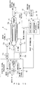
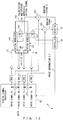
- FIG. 2 illustrates a configuration of an optical transmitter according to an embodiment of the present invention.
- An optical transmitter 2 of the embodiment illustrated in FIG. 2 includes a digital signal processor 20, D/A converters 12a and 12b, drivers 13a and 13b, a light source 14, an optical modulator 15, a photo detector 31, a multiplier 32, a detector 33, and a controller 34. Note that the optical transmitter 2 may include other unillustrated components.
- the digital signal processor 20 generates a drive signal I and a drive signal Q from input data. More specifically, the digital signal processor 20 generates the drive signal I and the drive signal Q by mapping the input data to a constellation for each symbol according to a specified modulation format. In addition, the digital signal processor 20 can generate the drive signal I and the drive signal Q so that an optical signal transmitted by the optical transmitter 2 has a desired characteristic. As an example, the drive signal I and the drive signal Q are generated so that the optical signal has a specified chromatic dispersion. In this case, the drive signal I and the drive signal Q are generated, for example, so as to provide dispersion pre-equalization for compensating for the chromatic dispersion in an optical transmission line.
- the digital signal processor 20 is implemented, for example, by a processor system including a processor element and a memory.
- the digital signal processor 20 maybe implemented by a hardware circuit.
- the digital signal processor 20 may be implemented by a combination of a processor system and a hardware circuit.
- the D/A converters 12a and 12b convert the drive signal I and the drive signal Q generated by the digital signal processor 20 to respective analog signals.
- the drivers 13a and 13b drive the optical modulator 15 with the drive signal I and the drive signal Q respectively outputted from the D/A converters 12a and 12b.
- the light source 14 generates continuous wave light.
- the light source 14 is implemented, for example, by a laser diode for generating a laser beam with a specified frequency.
- the optical modulator 15 includes a phase shifter 15a, an I arm modulation unit 15b, and a Q arm modulation unit 15c.
- the continuous wave light generated by the light source 14 is split by an optical splitter and guided to the I arm and the Q arm.
- the phase shifter 15a is implemented, for example, by an electrode formed near one of the I arm and the Q arm.
- the phase shifter 15a is assumed to be an electrode formed near the Q arm.
- the refractive index of the Q arm is changed and the optical path length of the Q arm is adjusted by controlling the bias voltage supplied to the phase shifter 15a. More specifically, the phase difference between light propagating through the I arm and light propagating through the Q arm (that is, "I-Q phase difference" or "the phase of the phase shifter 15a”) is adjusted by controlling the bias voltage supplied to the phase shifter 15a.
- the I arm modulation unit 15b and the Q arm modulation unit 15c are formed in the I arm and the Q arm, respectively.
- the I arm modulation unit 15b modulates the continuous wave light in response to the drive signal I to generate an optical signal.
- the Q arm modulation unit 15c modulates the continuous wave light in response to the drive signal Q to generate an optical signal.
- the I arm modulation unit 15b and the Q arm modulation unit 15c are respectively implemented, for example, by Mach-Zehnder interferometers.
- the optical modulator 15 combines the optical signal generated by the I arm modulation unit 15b and the optical signal generated by the Q arm modulation unit 15c to generate a modulated optical signal.
- the two optical signals are combined, for example, by a 2 ⁇ 2 optical coupler.
- the multiplier 21 multiplies the drive signal I and the drive signal Q.
- the multiplier 21 is implemented in the digital signal processor 20, but the multiplier 21 may be implemented outside the digital signal processor 20. Also in this example, the multiplier 21 multiplies the drive signal I and the drive signal Q in a digital domain, but may multiply the drive signal I and the drive signal Q in an analog domain. Further, the multiplier 21 may be configured to multiply the drive signals I and Q filtered by a low pass filter.
- the photo detector 31 converts the modulated optical signal generated by the optical modulator 15 to an electrical signal. Accordingly, an output signal of the photo detector 31 represents the modulated optical signal generated by the optical modulator 15. Note that the photo detector 31 may be implemented in the optical modulator 15 or may be implemented outside the optical modulator 15.
- the multiplier 32 multiplies the output signal of the photo detector 31 and the output signal of the multiplier 21. That is to say, the multiplier 21 and the multiplier 32 multiply the drive signal I, the drive signal Q, and the electrical signal representing the modulated optical signal generated by the optical modulator 15.
- the output signal of the multiplier 32 may be referred to as a "monitor signal”.
- the multiplier 32 may be implemented in the digital signal processor 20.
- a low pass filter may be provided between the photo detector 31 and the multiplier 32.
- the multiplier 21 and the multiplier 32 are an example of a multiplier circuit to generate a monitor signal.
- the detector 33 averages the monitor signal outputted from the multiplier 32 to detect an average value of the monitor signal.
- the monitor signal is averaged, for example, using a low pass filter. Note that a cutoff frequency of the low pass filter is assumed to be sufficiently lower than a symbol rate of the modulated optical signal. Note also that the detector 33 can detect a sign of the average value of the monitor signal. In this case, the detector 33 outputs monitor sign information representing whether the average value of the monitor signal is a positive value or a negative value.
- the controller 34 includes a phase controller 35 and a phase difference detector 36.
- the controller 34 is implemented, for example, by a processor system including a processor element and a memory.
- the controller 34 may be implemented by a hardware circuit.
- the controller 34 may be implemented by a combination of a processor system and a hardware circuit.
- the phase controller 35 controls the I-Q phase difference of the optical modulator 15 by controlling the bias voltage to be supplied to the phase shifter 15a. At this time, the phase controller 35 controls the I-Q phase difference to be a specified value. In this embodiment, the "specified value" is ⁇ /2+2 ⁇ or 3 ⁇ /2+2 ⁇ . More specifically, the phase controller 35 controls the bias voltage supplied to the phase shifter 15a so that the I-Q phase difference is adjusted to be ⁇ /2+2n ⁇ or 3 ⁇ /2+2n ⁇ .
- the method of controlling the I-Q phase difference to be ⁇ /2+2 ⁇ or 3 ⁇ /2+2n ⁇ is not particularly limited, but a well-known technique can be used.
- the phase controller 35 may control the I-Q phase difference to be ⁇ /2+2 ⁇ or 3 ⁇ /2+2n ⁇ by a method described in Japanese Laid-Open Patent Publication No. 2007-82094 , Japanese Laid-Open Patent Publication No. 2009-246578 , and Japanese Laid-Open Patent Publication No. 2007-259426 .
- the phase difference detector 36 detects the I-Q phase difference of the optical modulator 15 using a detection result by the detector 33. More specifically, the phase difference detector 36 detects the I-Q phase difference based on the average value of a product of the drive signal I, the drive signal Q, and the monitor signal representing the output modulated optical signal, or the sign of the average value thereof.
- the I-Q phase difference is controlled by the phase controller 35 to be ⁇ /2+2 ⁇ or 3 ⁇ /2+2 ⁇ .
- the phase difference detector 36 may decide whether the I-Q phase difference is either ⁇ /2+2 ⁇ or 3 ⁇ /2+2 ⁇ .
- the controller 34 notifies the digital signal processor 20 of the phase information representing the I-Q phase difference detected by the phase difference detector 36.
- the digital signal processor 20 generates (or corrects) the drive signal I and the drive signal Q based on the phase information. More specifically, the digital signal processor 20 generates (or corrects) the drive signal I and the drive signal Q based on whether the I-Q phase difference is either ⁇ /2+2 ⁇ or 3 ⁇ /2+2 ⁇ " .
- the optical transmitter 2 can generate the modulated optical signal appropriate for the I-Q phase difference of the optical modulator 15. In other words, the optical transmitter 2 may generate substantially the same modulated optical signal regardless whether the I-Q phase difference is controlled to be either ⁇ /2+2 ⁇ or 3 ⁇ /2+2 ⁇ .
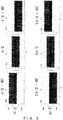
- FIGS. 3A and 3B illustrate a change in the monitor signal with respect to the I-Qphase difference of the optical modulator 15.
- the modulation format is 16-QAM. Note that in the following description, n/2+2nn may be referred to simply as ⁇ /2, and 3 ⁇ /2+2 ⁇ may be referred to simply as 3 ⁇ /2.
- FIG. 3A illustrates the monitor signal when the I-Q phase difference is controlled to be ⁇ /2 or around ⁇ /2.
- the monitor signal is distributed around zero.
- an average value of the monitor signal is zero.
- zero is assumed to include “approximately zero” or “substantially zero”.
- the monitor signal When the I-Q phase difference is ⁇ /2 - 45 degrees, the monitor signal is distributed on the positive side in this example. Thus, the detector 33 detects a positive value. Meanwhile, when the I-Q phase difference is ⁇ /2 + 45 degrees, the monitor signal is distributed on the negative side in this example. Thus, the detector 33 detects a negative value.
- the sign of a value detected by the detector 33 may be referred to as a "monitor sign". For example, when the detector 33 detects the positive value, the monitor sign is "positive” ; and when the detector 33 detects the negative value, the monitor sign is "negative".
- FIG. 3B illustrates the monitor signal when the I-Q phase difference is controlled to be 3 ⁇ /2 or around 3 ⁇ /2.
- the monitor signal is distributed around zero in the same manner as when the I-Q phase difference is ⁇ /2.
- the detector 33 also detects zero when the I-Q phase difference is 3 ⁇ /2.
- the monitor signal When the I-Q phase difference is 3 ⁇ /2 - 45 degrees, the monitor signal is distributed on the negative side in this example . Thus, “negative” is detected as the monitor sign. Meanwhile, when the I-Q phase difference is 3 ⁇ /2 + 45 degrees, the monitor signal is distributed on the positive side in this example. Thus, the monitor sign is "positive".
- the phase controller 35 may control the bias voltage supplied to the phase shifter 15a so that the detector 33 detects zero.
- the phase controller 35 may control the bias voltage so that the average value detected by the detector 33 approaches zero.
- the phase difference detector 36 may decide whether the I-Q phase difference is controlled to be either ⁇ /2 or 3 ⁇ /2 using the change in the monitor sign.
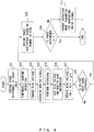
- FIG. 4 is a flowchart illustrating a first method of controlling an operation mode of the optical transmitter.
- the process of this flowchart is executed, for example, before the optical transmitter 2 starts a communication service or when the optical transmitter 2 is in maintenance.
- the digital signal processor 20 generates the drive signal I and the drive signal Q.
- the optical transmitter 2 generates the modulated optical signal by mapping the input data to a corresponding signal point for each symbol in a multi-level modulation format. Note that the distribution of symbols to be mapped to each of the signal points (for example, four signal points for the QPSK and 16 signal points for the 16QAM) is assumed to be uniform or nearly uniform.
- the operation mode of the optical transmitter 2 (or the parameter for generating the drive signal from the input data) is set assuming that the I-Q phase difference of the optical modulator 15 is ⁇ /2.
- the operation mode of the optical transmitter 2 is assumed to be controlled so that the optical modulator 15 generates a specified modulated optical signal when the I-Q phase difference is ⁇ /2.
- step S1 the phase controller 35 controls the bias voltage supplied to the phase shifter 15a to be an initial value.
- the initial value is not particularly limited, but, for example, is near zero volt.
- step S2 the detector 33 acquires the monitor signal outputted from the multiplier 32.
- the monitor signal is generated by multiplying the drive signal I, the drive signal Q, and the electrical signal representing the output modulated optical signal as described above.
- step S3 the detector 33 averages the monitor signal. Then, the detector 33 outputs the monitor sign information representing whether the average value of the monitor signal is a positive value or a negative value.
- step S4 the phase difference detector 36 saves the monitor sign information acquired in S3 associated with the current bias voltage.
- step S5 the phase controller 35 updates the bias voltage to be supplied to the phase shifter 15a.
- step S6 the phase controller 36 decides whether the new bias voltage Vn exceeds the voltage sweep range .
- the voltage sweep range is determined, for example, based on a change in voltage causing the I-Q phase difference to shift by 2 ⁇ . For example, the voltage sweep range is determined so that the I-Q phase difference shifts by 2 ⁇ or more when the bias voltage changes from a minimum value to a maximum value of the voltage sweep range.
- steps S2-S6 are executed repeatedly until the bias voltage Vn exceeds the voltage sweep range.
- the operation of repeatedly executing steps S2-S6 corresponds to the process of collecting the monitor sign information while sweeping the bias voltage.
- FIG. 5 illustrates an example of the phase difference decision information generated in steps S2-S6.
- the phase difference decision information represents the sign of the average value of the monitor signal with respect to the bias voltage.
- the monitor sign changes from positive to negative.
- the monitor sign changes from negative to positive.
- the bias voltage increases from 8 volts to 10 volts
- step S7 the phase controller 35 controls the I-Q phase difference of the optical modulator 15 to be a target value.
- the target value of the I-Q phase difference is ⁇ /2.
- the method of controlling the I-Q phase difference to be the target value is not particularly limited.
- the phase controller 35 may control the I-Q phase difference to be the target value by a method described in Japanese Laid-Open Patent Publication No. 2007-82094 , Japanese Laid-Open Patent Publication No. 2009-246578 , and Japanese Laid-Open Patent Publication No. 2007-259426 .
- the phase controller 35 adjusts the I-Q phase difference to be the target value by controlling the bias voltage so that the average value of the monitor signal outputted from the multiplier 33 approaches zero (or to be zero) .
- this method controls the I-Q phase difference to be either ⁇ /2 or 3 ⁇ /2.
- the phase difference detector 36 decides whether the I-Q phase difference is controlled to be either ⁇ /2 or 3 ⁇ /2.
- step S8 the phase difference detector 36 detects the bias voltage when the I-Q phase difference converges to the target value. In other words, the phase difference detector 36 detects the bias voltage when the process of step S7 completes. In the following description, the bias voltage detected in step S8 may be referred to as a "converged bias voltage".
- step S9 the phase difference detector 36 extracts data corresponding to the bias voltage near the converged bias voltage from the phase difference decision information.
- the phase difference detector 36 extracts multiple sets of data from the phase difference decision information. For example, in steps S2-S6, the phase difference decision information illustrated in FIG. 5 is assumed to be generated.
- the bias voltage that is, the converged bias voltage
- the phase difference detector 36 acquires data corresponding to a bias voltage less than the converged bias voltage and data corresponding to a bias voltage greater than the converged bias voltage near the converged bias voltage. As a result, "4.0 volts, negative” and "6.0 volts, positive" are obtained.
- the phase difference detector 36 decides whether the I-Q phase difference is controlled to be either ⁇ /2 or 3 ⁇ /2 based on the multiple sets of data acquired in step S9.
- the changes in monitor signal for the I-Q phase difference are assumed to be as illustrated in FIGS. 3A and 3B . In this case, when the monitor sign information changes from "positive" to "negative” as the bias voltage increases, the phase difference detector 36 decides that the I-Q phase difference is controlled to be ⁇ /2.
- the phase difference detector 36 decides that the I-Q phase difference is controlled to be 3 ⁇ /2. Then, the controller 34 notifies the digital signal processor 20 of the phase information representing a detection result by the phase difference detector 36.
- steps S8-S11 may be performed with various patterns. For example, when two sets of data are extracted from the phase difference decision information, the decision is performed as follows.
- the digital signal processor 20 decides the operation mode of the optical transmitter 2 according to the phase information received from the controller 34.
- the initial operation mode of the optical transmitter 2 is set to an operation mode corresponding to the I-Q phase difference ⁇ /2 when the process of this flowchart starts.
- the I-Q phase difference is controlled to be ⁇ /2 (S11: Yes)
- the process of the optical transmitter 2 ends.
- the digital signal processor 20 executes the process in step S12.
- step S12 the digital signal processor 20 changes the parameter for generating the drive signal I and the drive signal Q from the input data so as to generate substantially the same modulated optical signal as that when the I-Q phase difference is controlled to be ⁇ /2. Note that the method of changing the parameter based on the phase information will be described in detail later.
- the optical transmitter 2 of the embodiment decides whether the I-Q phase difference of the optical modulator 15 is controlled to be either ⁇ /2 or 3 ⁇ /2, and then generates the modulated optical signal using a parameter (or an operation mode) according to the decision result.
- the optical transmitter 2 can generate substantially the same modulated optical signal regardless of whether the I-Q phase difference is controlled to be either ⁇ /2 or 3 ⁇ /2.
- the use of the optical transmitter 2 of the embodiment in the optical transmission system allows the optical receiver to recover data from the modulated optical signal without switching the demodulation operation according to the settings of the I-Q phase difference of the optical modulator 15.
- the method of deciding whether the I-Q phase difference is either ⁇ /2 or 3 ⁇ /2 is not limited to the aforementioned embodiment, but the optical transmitter 2 may detect the I-Q phase difference by another method.
- FIG. 6 is a flowchart illustrating a second method of controlling the operation mode of the optical transmitter.
- the optical transmitter 2 may execute the process of the flowchart illustrated in FIG. 6 instead of the flowchart illustrated in FIG. 4 .
- step S21 the phase controller 35 controls the I-Q phase difference of the optical modulator 15 to be a specified target value.
- the I-Q phase difference is controlled to be either ⁇ /2 or 3 ⁇ /2. Note that in the description of the flowchart of FIG. 6 , the bias voltage when the I-Qphase difference converges to ⁇ /2 or 3 ⁇ /2 is also assumed to be referred to as a "converged bias voltage".
- step S22 the optical transmitter 2 temporarily suspends the operation.
- step S23 the phase controller 35 changes the bias voltage. At this time, the phase controller 35 determines a new bias voltage, for example, by reducing the current bias voltage (that is, the converged bias voltage) by a specified value.
- Steps S24-S28 are substantially the same as steps S2-S6 of FIG. 4 . More specifically, the controller 34 generates the phase difference decision information illustrated in FIG. 5 by sweeping the bias voltage. Note that in the method illustrated in FIG. 6 , the converged bias voltage has already been detected when steps S24-S28 are executed. Thus, the controller 34 may generate the phase difference decision information only in a region near the converged bias voltage. Inthiscase, the voltage sweep range in step S28 is narrower than the voltage sweep range in step S6 of FIG. 4 . Thus, the time required to generate the phase difference decision information by the method illustrated in FIG. 6 may be shorter than that by the method illustrated in FIG. 4 .
- controller 34 may not sweep the bias voltage insteps S24-S28 .
- the controller 34 may only acquire the monitor sign information for "converged bias voltage - ⁇ V" and "converged bias voltage + ⁇ V".
- Steps S29 and S30 are substantially the same as steps S10 and S11 of FIG. 4 . More specifically, the phase difference detector 36 decides whether the I-Q phase difference is controlled to be either ⁇ /2 or 3 ⁇ /2 based on the phase difference decision information generated in steps S24-S28. Then, the digital signal processor 20 decides the operation mode of the optical transmitter 2 according to the phase information received from the controller 34. More specifically, if the I-Q phase difference is controlled to be ⁇ /2 (S30: Yes), the process of the optical transmitter 2 ends. If the I-Q phase difference is not controlled to be ⁇ /2 (S30: No), the digital signal processor 20 executes the process in step S12.
- FIG. 7 is a flowchart illustrating a third method of controlling the operation mode of the optical transmitter.
- the optical transmitter 2 may execute the process of the flowchart illustrated in FIG. 7 instead of the flowchart illustrated in FIG. 4 .
- Steps S31 and S32 are substantially the same as steps S21 and S22 of FIG. 6 . More specifically, the I-Q phase difference is controlled to be either ⁇ /2 or 3 ⁇ /2. Note that in the description of the flowchart of FIG. 7 , the bias voltage when the I-Q phase difference converges to ⁇ /2 or 3 ⁇ /2 is also assumed to be referred to as a "converged bias voltage".
- step S33 the phase controller 35 superimposes a low-frequency signal on the converged bias voltage.
- the frequency of the low-frequency signal is assumed to be sufficiently lower than the data rate or symbol rate.
- the optical transmitter 2 includes a low-frequency signal generation circuit for generating a low-frequency signal and the phase controller 35 is assumed to include a circuit for superimposing the low-frequency signal on the bias voltage.
- step S34 the detector 33 detects a low- frequency signal component from the monitor signal by synchronous detection.
- the synchronous detection is implemented, for example, by multiplying the aforementioned low-frequency signal by the monitor signal.
- the detector 33 is assumed to have a circuit for multiplying the monitor signal by the low-frequency signal generated by the aforementioned low-frequency signal generation circuit.
- the phase difference detector 36 detects the I-Q phase difference based on the synchronous detection result. More specifically, if the low-frequency signal component detected from the monitor signal is in-phase with the low-frequency signal generated by the low-frequency signal generation circuit, the phase difference detector 36 decides that the I-Q phase difference is one of ⁇ /2 and 3 ⁇ /2 (for example, ⁇ /2). Meanwhile, if the low-frequency signal component detected from the monitor signal is reverse phase with the low-frequency signal generated by the low-frequency signal generation circuit, the phase difference detector 36 decides that the I-Q phase difference is the other one of ⁇ /2 and 3 ⁇ /2 (for example, 3 ⁇ /2).
- the digital signal processor 20 decides the operation mode of the optical transmitter 2 according to the phase information received from the controller 34 in the same procedure as illustrated in FIG. 4 or FIG. 6 . More specifically, if the I-Q phase difference is controlled to be ⁇ /2 (S36 : Yes) , the process of the optical transmitter 2 ends. Meanwhile, if the I-Q phase difference is not controlled to be ⁇ /2 (S36: No), the digital signal processor 20 executes the process in step S12.
- steps S32 and S33 of FIG. 7 may not be executed.
- the amplitude of the low-frequency signal may be changed when the control of the flowchart illustrated in FIG. 7 is executed.
- the optical transmitter 2 can decide whether the I-Q phase difference is controlled to be either ⁇ /2 or 3 ⁇ /2. Then, the digital signal processor 20 sets the operation mode (that is, the parameter for generating the drive signal I and the drive signal Q from the input data) according to the decision result.
- the operation mode that is, the parameter for generating the drive signal I and the drive signal Q from the input data
- FIG. 8 is a block diagram describing functions of the digital signal processor 20.
- the digital signal processor 20 includes a mapper 22, a dispersion pre-equalizer 23, and a frequency offset adder 24.
- the multiplier 21 is implemented in the digital signal processor 20 and multiplies the drive signal I and the drive signal Q in a digital domain.
- the frequency offset adder 24 is located on the output side of the dispersion pre-equalizer 23, but the frequency offset adder 24 may be located on the input side of the dispersion pre-equalizer 23.
- the digital signal processor 20 may include other functions . Note further that the digital signal processor 20 may not have the dispersion pre-equalizer 23 and may not have the frequency offset adder 24.
- the mapper 22 maps the input data to a corresponding signal point for each symbol according to the specified modulation format. For example, in the QPSK or DQPSK, one symbol is generated every two bits. In the 16QAM, one symbol is generated every four bits.
- FIGS. 9A and 9B illustrate examples of a QPSK constellation.
- mapping illustrated in FIG. 9A is performed. More specifically, data “00” is mapped to signal point A. Likewise, data “10”, “11”, and “01” is mapped to signal points B, C, and D respectively.
- the mapper 22 outputs a set of signals E1 and F1 respectively according to the following mapping pattern 1.
- the I-Q phase difference of the optical modulator 15 may be controlled to be not ⁇ /2 but 3 ⁇ /2 as described above. If the input data is mapped according to the mapping pattern 1 when the I-Q phase difference is 3 ⁇ /2, the modulated optical signal generated by the optical modulator 15 is different from the modulated optical signal generated when the I-Q phase difference is ⁇ /2. More specifically, if the input data is mapped according to the mapping pattern 1 when the I-Q phase difference is 3 ⁇ /2, the modulated optical signal corresponding to the constellation illustrated in FIG. 9B is generated.
- the mapper 22 selects a mapping pattern according to the phase information notified from the controller 34. More specifically, if the phase information represents the I-Q phase difference ⁇ /2, the mapper 22 maps the input data to a corresponding signal point for each symbol according to the mapping pattern 1. Meanwhile, if the phase information represents the I-Q phase difference 3 ⁇ /2, the mapper 22 maps the input data to a corresponding signal point for each symbol according to the mapping pattern 2. In this case, even if the I-Q phase difference of the optical modulator 15 is 3 ⁇ /2, the digital signal processing generates the same modulated optical signal as that when the I-Q phase difference of the optical modulator 15 is controlled to be ⁇ /2 . In other words, the optical modulator 15 can generate substantially the same modulated optical signal regardless of whether the I-Q phase difference is controlled to be either ⁇ /2 or 3 ⁇ /2.
- n/2 is an expected I-Q phase difference.
- the digital signal processor 20 maps the input data according to the mapping pattern 1.
- the digital signal processor 20 maps the input data according to the mapping pattern 2.
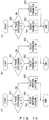
- FIG. 10A is a flowchart illustrating a process of setting the operation mode of the mapper 22.
- the process of the flowchart is executed by the digital signal processor 20 when the phase information representing the I-Q phase difference is generated by the method illustrated in FIG. 4 , FIG. 6 , or FIG. 7 .
- step S41 the digital signal processor 20 acquires the phase information from the controller 34 and detects whether the I-Q phase difference is ⁇ /2 or not. If the I-Q phase difference is ⁇ /2, the process moves to step S42, in which the digital signal processor 20 sets the operation mode or the operation parameter of the mapper 22 so as to map the input data to a corresponding signal point for each symbol according to the mapping pattern 1. Meanwhile, if the I-Q phase difference is 3 ⁇ /2, the process moves to step S43, in which the digital signal processor 20 sets the operation mode or the operation parameter of the mapper 22 so as to map the input data to a corresponding signal point for each symbol according to the mapping pattern 2.
- the process of step S43 is an example of the process of step S12 illustrated in FIG. 4 , FIG. 6 , or FIG. 7 .
- the mapper 22 is configured to select the mapping pattern 1 when the flowchart starts.
- the digital signal processor 20 may not execute the process of step S42.
- the I-Q phase difference is 3 ⁇ /2 (S41: No)
- the process moves to step S43, in which the digital signal processor 20 controls the mapper 22 so as to select the mapping pattern 2.
- the dispersion pre-equalizer 23 corrects the signals E1 and F1 outputted from the mapper 22 so as to add a specified chromatic dispersion to the modulated optical signal transmitted from the optical transmitter 2.
- the "specified chromatic dispersion” is determined, for example, so as to compensate for a chromatic dispersion of an optical transmission line between the optical transmitter 2 and the optical receiver. In this case, it is preferable that the chromatic dispersion of the optical transmission line is measured in advance.
- the dispersion pre-equalizer 23 can add desired chromatic dispersion to the modulated optical signal, for example, by generating the signals E2 and F2 by multiplying the signals E1 and F1 by matrix D.
- the matrix D is, for example, an inverse matrix of a matrix representing the chromatic dispersion of the optical transmission line between the optical transmitter 2 and the optical receiver.
- FIG. 10B is a flowchart illustrating a process of setting the operation mode of the dispersion pre-equalizer 23.
- the process of the flowchart is executed by the digital signal processor 20 when the phase information representing the I-Q phase difference is generated by the method illustrated in FIG. 4 , FIG. 6 , or FIG. 7 .
- step S51 the digital signal processor 20 acquires the phase information from the controller 34 and detects whether the I-Q phase difference is ⁇ /2 or not. If the I-Q phase difference is ⁇ /2, the process moves to step S52, in which the digital signal processor 20 supplies parameter 1 to the dispersion pre-equalizer 23 so as to perform pre-equalization for compensating for the chromatic dispersion of the optical transmission line.
- the parameter 1 represents a chromatic dispersion for compensating for the chromatic dispersion of the optical transmission line and is supplied to the dispersion pre-equalizer 23 as an element of the aforementioned matrix D.
- step S53 the digital signal processor 20 sets parameter 2 to the dispersion pre-equalizer 23.
- the parameter 2 is obtained by reversing the sign of the parameter 1. For example, when the parameter 1 represents "500 ps/nm", the parameter 2 represents "-500 ps/nm".
- the frequency offset adder 24 corrects the signals E2 and F2 so as to compensate for the difference between a frequency of the light source 14 of the optical transmitter 2 and a frequency of local oscillation light used by the optical coherent receiver to receive the optical signal.
- the signals E2 and F2 represent signals inputted to the frequency offset adder 24 and are outputted from the dispersion pre-equalizer 23 in the example illustrated in FIG. 8 .
- the correction for supplying a frequency offset to the optical signal is implemented by the following rotation calculation.
- I and Q indicate output signals of the frequency offset adder 24.
- ⁇ (t) indicates an angle corresponding to the frequency offset added to the optical signal.
- I E 2 cos ⁇ t ⁇ F 2 sin ⁇ t
- Q E 2 sin ⁇ t + F 2 cos ⁇ t
- FIG. 10C is a flowchart illustrating a process of setting the operation mode of the frequency offset adder 24 .
- the process of the flowchart is executed by the digital signal processor 20 when the phase information representing the I-Q phase difference is generated by the method illustrated in FIG. 4 , FIG. 6 , or FIG. 7 .
- step S61 the digital signal processor 20 acquires the phase information from the controller 34 and detects whether the I-Q phase difference is ⁇ /2 or not. If the I-Q phase difference is ⁇ /2, the process moves to step S62, in which the digital signal processor 20 supplies the parameter 3 to the frequency offset adder 24 so as to compensate for the frequency offset between the optical transmitter 2 and the optical receiver.
- the parameter 3 is represented by ⁇ of the aforementioned rotation calculation.
- step S63 the digital signal processor 20 sets the parameter 4 to the frequency offset adder 24.
- the parameter 4 is obtained by reversing the sign of the parameter 3. More specifically, if the parameter 3 is " ⁇ " the parameter 4 is "- ⁇ ".
- the I-Q phase difference of the optical modulator 15 is controlled to be either ⁇ /2 or 3 ⁇ /2.
- the optical transmitter 2 decides whether the I-Q phase difference of the optical modulator 15 is controlled to be either ⁇ /2 or 3 ⁇ /2, and then generates the modulated optical signal using a parameter (or an operation mode) according to the decided result.
- the optical transmitter 2 can generate substantially the same modulated optical signal regardless of whether the I-Q phase difference is controlled to be either ⁇ /2 or 3 ⁇ /2.
- the optical receiver need not execute the process of detecting the I-Q phase difference when data is recovered from the modulated optical signal. This results in reducing the processing amount of the optical receiver. Particularly in the multi-level modulation with a large number of bits per symbol, power consumption of the optical receiver is reduced.
- the optical transmitter of the present embodiment can provide a desired dispersion pre-equalization and/or a desired frequency offset regardless of whether the I-Q phase difference is controlled to be either ⁇ /2 or 3 ⁇ /2. This improves the characteristics of the modulated optical signal or suppresses the deterioration of the characteristics of the modulated optical signal.
- the digital signal processor 20 if the I-Q phase difference is controlled to be 3 ⁇ /2, the digital signal processor 20 generates the same optical signal as that when the I-Q phase difference is controlled to be ⁇ /2, by changing the parameter for generating the drive signal. In other words, if the I-Q phase difference is controlled to be 3 ⁇ /2, the digital signal processing provides a state equivalent to that when the I-Q phase difference is controlled to be ⁇ /2.
- the present invention is not limited to this configuration.
- the optical transmitter according to the present invention may adjust the I-Q phase difference to be ⁇ /2 by controlling the bias voltage.
- the phase controller 35 controls the bias voltage to be supplied to the phase shifter 15a so that the I-Q phase difference detected by the phase difference detector 36 approaches the target value (that is, ⁇ /2).
- the method of providing an equivalent operation state in which the I-Q phase difference is ⁇ /2 by the digital signal processing is more preferable than the method of adjusting the I-Q phase difference to be from 3 ⁇ /2 to ⁇ /2 by controlling the bias voltage.
- the output signal of the multiplier 21 representing the product of the drive signal I and the drive signal Q indicates a constellation state.
- the average value of the output signal of the multiplier 21 is substantially zero.
- the I-Q phase difference is controlled to be ⁇ /2 or 3 ⁇ /2
- the average value of the monitor signal is substantially zero.
- the average value of the output signal of the multiplier 21 is not zero.
- the average value of the monitor signal may not be zero. In other words, in this case, it is not decided with high precision whether the I-Q phase difference is controlled to be either ⁇ /2 or 3 ⁇ /2 .
- the output signal of the multiplier 21 may be used as an indicator indicating the precision of the detection of the I-Q phase difference.
- FIG. 11 illustrates a configuration of an optical transmitter according to another embodiment.
- the optical transmitter 3 illustrated in FIG. 11 generates a monitor signal by a method different from the optical transmitter 2 illustrated in FIG. 2 .
- the digital signal processor 40 generates the drive signal I and the drive signal Q from the input data in the same manner as the digital signal processor 20 illustrated in FIG. 2 .
- the digital signal processor 40 includes bit converters 41a and 41b and an exclusive OR circuit 42.
- the bit converter 41a converts an n-bit drive signal I into one-bit converted signal I.
- the conversion method is not particularly limited, but is implemented, for example, by extracting the drive signal I for each n bit and sampling one bit from each n-bit signal.
- the bit converter 41b coverts an n-bit drive signal Q into one-bit converted signal Q.
- "n" is an integer of 2 or more.
- the exclusive OR circuit 42 outputs an exclusive OR between the converted signal I and the converted signal Q. Then, the multiplier 32 generates a monitor signal by multiplying an output signal of the exclusive OR circuit 42 by an electrical signal representing the output modulated optical signal. Note that the digital signal processor 40 may include an averaging circuit 43 for averaging the output signal of the exclusive OR circuit 42.
- the drive signals I and Q are multiplied to generate the monitor signal.
- the optical transmitter 3 illustrated in FIG. 11 performs an exclusive OR between the converted signals I and Q.
- the speed of the converted signals I and Q is 1/n of the drive signals I and Q.
- the configuration illustrated in FIG. 11 reduces the size of an arithmetic circuit or the number of operations of the digital signal processor 20.
- FIG. 12 illustrates a configuration of an optical transmitter according to still another embodiment.
- the optical transmitter 4 illustrated in FIG. 12 can generate a polarization multiplexed modulated optical signal.
- the optical transmitter 4 includes a digital signal processor 50, a light source 14, optical modulators 15X and 15Y, a polarization multiplexer 15Z, photo detectors 31X and 31Y, multipliers 32X and 32Y, a detector 33, and controller 34.
- the digital signal processor 50 generates drive signals XI, XQ, YI, and YQ from input data.
- the continuous wave light generated by the light source 14 is guided to the optical modulators 15X and 15Y.
- the optical modulator 15X generates the modulated optical signal X by modulating the continuous wave light in response to the drive signals XI and XQ.
- the optical modulator 15Y generates the modulated optical signal Y by modulating the continuous wave light in response to the drive signals YI and YQ.
- the polarization multiplexer 15Z generates a polarization multiplexed modulated optical signal from the modulated optical signal X and the modulated optical signal Y.
- the method of generating the monitor signals X and Y is substantially the same as that for the optical transmitter 2 illustrated in FIG. 2 . More specifically, the multiplier 21X multiplies the drive signal XI and the drive signal XQ. The photo detector 31X converts the modulated optical signal X into an electrical signal. The multiplier 32X generates the monitor signal X by multiplying an output signal of the multiplier 21X by anelectrical signal representing the modulated optical signal X. Likewise, the multiplier 21Y, the photo detector 31Y, and the multiplier 32Y generate the monitor signal Y.
- the detector 33 outputs monitor sign information corresponding to each of the monitor signals X and Y.
- the controller 34 detects the I-Q phase difference of the optical modulator 15X based on the monitor sign information of the monitor signal X, and detects the I-Q phase difference of the optical modulator 15Y based on the monitor sign information of the monitor signal Y.
- the method of detecting the corresponding I-Q phase difference based on the monitor signals X and Y is substantially the same as that for the optical transmitter 2 illustrated in FIG. 2 .
- the controller 34 notifies the digital signal processor 50 of the phase information X and Y each representing the detection result.
- the digital signal processor 50 sets parameters for generating the drive signals XI and XQ from the input data based on the phase information X. In addition, the digital signal processor 50 sets parameters for generating the drive signals YI and YQ from the input data based on the phase information Y.
- the method of setting the parameters based on the phase information X and Y is substantially the same as that for the optical transmitter 2 illustrated in FIG. 2 .
- the controller 34 may detect the I-Q phase differences of the optical modulators 15Xand 15Y inparallel. Alternatively, the controller 34 may detect the I-Q phase difference of one of the optical modulators 15X and 15Y and then may detect the I-Q phase difference of the other one of the optical modulators 15X and 15Y.
Landscapes
- Physics & Mathematics (AREA)
- Electromagnetism (AREA)
- Engineering & Computer Science (AREA)
- Computer Networks & Wireless Communication (AREA)
- Signal Processing (AREA)
- Optics & Photonics (AREA)
- Optical Modulation, Optical Deflection, Nonlinear Optics, Optical Demodulation, Optical Logic Elements (AREA)
- Optical Communication System (AREA)
Claims (15)
- Optischer Sender, umfassend:einen optischen Modulator (15), der eine erste Modulationseinheit und eine zweite Modulationseinheit aufweist, die jeweils konfiguriert sind, um Eingangslicht als Reaktion auf ein erstes Ansteuersignal und ein zweites Ansteuersignal zu modulieren, um ein erstes optisches Signal und ein zweites optisches Signal zu generieren;einen Signalgenerator (20), der konfiguriert ist, um das erste Ansteuersignal und das zweite Ansteuersignal zu generieren, die jeweils der ersten Modulationseinheit und der zweiten Modulationseinheit zugeführt werden;eine Phasensteuervorrichtung (35), die konfiguriert ist, um eine Phasendifferenz zwischen dem ersten optischen Signal und dem zweiten optischen Signal in dem optischen Modulator anzupassen; undeinen Phasendifferenzdetektor (36), der konfiguriert ist, um die von der Phasensteuervorrichtung gesteuerte Phasendifferenz zwischen dem ersten optischen Signal und dem zweiten optischen Signal zu detektieren, wobeider Signalgenerator konfiguriert ist, um das erste Ansteuersignal und das zweite Ansteuersignal basierend auf der durch den Phasendifferenzdetektor detektierten Phasendifferenz zu generieren,dadurch gekennzeichnet, dass der optische Sender weiter umfasst:eine Multiplizierschaltung (21, 32), die konfiguriert ist, um das erste Ansteuersignal, das zweite Ansteuersignal und ein elektrisches Signal, das ein Ausgangssignal des optischen Modulators darstellt, zu multiplizieren, wobeider Phasendifferenzdetektor konfiguriert ist, um die Phasendifferenz basierend auf einem Ausgangssignal der Multiplizierschaltung zu detektieren.
- Optischer Sender nach Anspruch 1, wobei der Signalgenerator konfiguriert ist, um einen Parameter zum Generieren des ersten Ansteuersignals und des zweiten Ansteuersignals aus Eingangsdaten basierend auf der durch den Phasendifferenzdetektor detektierten Phasendifferenz zu steuern.
- Optischer Sender nach Anspruch 1, wobei der Signalgenerator konfiguriert ist, um das erste Ansteuersignal und das zweite Ansteuersignal durch Abbilden der Eingangsdaten auf einer Konstellation basierend auf der durch den Phasendifferenzdetektor detektierten Phasendifferenz zu generieren.
- Optischer Sender nach Anspruch 1, wobei der Signalgenerator einen chromatischen Dispersionsvorentzerrer hat, der konfiguriert ist, um eine chromatische Dispersion zu steuern, die zu dem durch den optischen Modulator generierten optischen Signal hinzugefügt werden soll, und
der chromatische Dispersionsvorentzerrer konfiguriert ist, um das erste Ansteuersignal und das zweite Ansteuersignal zu generieren, sodass die chromatische Dispersion, die der durch den Phasendifferenzdetektor detektierten Phasendifferenz entspricht, zu dem optischen Signal hinzugefügt wird. - Optischer Sender nach Anspruch 1, wobei der Signalgenerator eine Frequenzverschiebungssteuervorrichtung hat, die konfiguriert ist, um eine Frequenzverschiebung, die zu dem durch den optischen Modulator generierten optischen Signal hinzugefügt werden soll, zu steuern, und
die Frequenzverschiebungssteuervorrichtung konfiguriert ist, um das erste Ansteuersignal und das zweite Ansteuersignal zu generieren, sodass die Frequenzverschiebung, die der durch den Phasendifferenzdetektor detektierten Phasendifferenz entspricht, zu dem optischen Signal hinzugefügt wird. - Optischer Sender nach Anspruch 1, wobei die Phasensteuervorrichtung konfiguriert ist, um die Phasendifferenz zwischen dem ersten optischen Signal und dem zweiten optischen Signal zu steuern, um ein erster spezifizierter Wert oder ein zweiter spezifizierter Wert zu sein; und
der Phasendifferenzdetektor konfiguriert ist, um basierend auf dem Ausgangssignal der Multiplizierschaltung zu entscheiden, ob die Phasendifferenz zwischen dem ersten optischen Signal und dem zweiten optischen Signal gesteuert wird, um entweder der erste spezifizierte Wert oder der zweite spezifizierte Wert zu sein. - Optischer Sender nach Anspruch 6, wobei der Signalgenerator konfiguriert ist, um das erste Ansteuersignal und das zweite Ansteuersignal basierend darauf, ob die Phasendifferenz zwischen dem ersten optischen Signal und dem zweiten optischen Signal gesteuert wird, um entweder der erste spezifizierte Wert oder der zweite spezifizierte Wert zu sein, zu generieren.
- Optischer Sender nach Anspruch 6, wobei der erste spezifizierte Wert π/2 + 2nπ ist und der zweite spezifizierte Wert 3π/2 + 2nπ ist, wobei n eine beliebige ganze Zahl einschließlich Null ist.
- Optischer Sender nach Anspruch 1, wobei die Phasensteuervorrichtung konfiguriert ist, um die Phasendifferenz zwischen dem ersten optischen Signal und dem zweiten optischen Signal durch Steuern einer Vorspannung, die dem optischen Modulator zugeführt wird, zu steuern, um der erste spezifizierte Wert oder der zweite spezifizierte Wert zu sein; und
der Phasendifferenzdetektor konfiguriert ist, um die Vorspannung zu detektieren, wenn die Phasendifferenz zwischen dem ersten optischen Signal und dem zweiten optischen Signal gesteuert wird, um der erste spezifizierte Wert oder der zweite spezifizierte Wert zu sein, und basierend auf einer Änderung in dem Ausgangssignal der Multiplizierschaltung nahe der detektierten Vorspannung entscheidet, ob die Phasendifferenz zwischen dem ersten optischen Signal und dem zweiten optischen Signal gesteuert wird, um entweder der erste spezifizierte Wert oder der zweite spezifizierte Wert zu sein. - Optischer Sender nach Anspruch 1, wobei die Multiplizierschaltung einen ersten Multiplizierer, der konfiguriert ist, um das erste Ansteuersignal und das zweite Ansteuersignal zu multiplizieren, und einen zweiten Multiplizierer, der konfiguriert ist, um ein Ausgangssignal des ersten Multiplizierers mit einem elektrischen Signal, das das Ausgangssignal des optischen Modulators darstellt, zu multiplizieren, aufweist; und
eine Präzision des Detektierens durch den Phasendifferenzdetektor basierend auf dem Ausgangssignal des ersten Multiplizierers entschieden wird. - Optischer Sender nach Anspruch 1, wobei die Phasensteuervorrichtung konfiguriert ist, um die Phasendifferenz zwischen dem ersten optischen Signal und dem zweiten optischen Signal durch Steuern der Vorspannung, die dem optischen Modulator zugeführt wird, zu steuern.
- Optischer Sender nach Anspruch 11, wobei die Phasensteuervorrichtung konfiguriert ist, um die Vorspannung, die dem optischen Modulator zugeführt wird, zu steuern, sodass die durch den Phasendifferenzdetektor detektierte Phasendifferenz, sich einem spezifischen Wert annähert.
- Optischer Sender nach Anspruch 1, weiter umfassend:einen Wandler (41a, 41b), der konfiguriert ist, um das erste Ansteuersignal in ein erstes umgewandeltes Signal umzuwandeln, das eine Anzahl von Bits hat, die kleiner als das erste Ansteuersignal ist, und um das zweite Ansteuersignal in ein zweites umgewandeltes Signal umzuwandeln, das eine Anzahl von Bits hat, die kleiner als das zweite Ansteuersignal ist;einen Multiplizierer (42), der konfiguriert ist ein exklusives ODER-Signal zwischen dem ersten umgewandelten Signal und dem zweiten umgewandelten Signal mit einem elektrischen Signal, das ein Ausgangssignal des optischen Modulators darstellt, zu multiplizieren; und wobeider Phasendifferenzdetektor (36) konfiguriert ist, um die Phasendifferenz basierend auf dem Ausgangssignal des Multiplizierers zu detektieren.
- Optischer Sender nach Anspruch 1, wobei der optische Modulator (15) einen ersten optischen Modulator (15X) darstellt und weiter umfassend:einen zweiten optischen Modulator (15Y), der eine dritte Modulationseinheit und eine vierte Modulationseinheit aufweist, die konfiguriert sind, um Eingangslicht als Reaktion auf ein erstes Ansteuersignal und ein zweites Ansteuersignal zu modulieren, um ein drittes optisches Signal und ein viertes optisches Signal zu generieren;einen Polarisationsmultiplexer (15Z), der konfiguriert ist, um ein polarisationsmultiplexiertes Signal von einem ersten modulierten optischen Signal, das von dem ersten optischen Modulator ausgegeben wird, und von einem zweiten modulierten optischen Signal, das von dem zweiten optischen Modulator ausgegeben wird, zu generieren;wobei der Signalgenerator (20; 50) konfiguriert ist, um ein drittes Ansteuersignal und ein viertes Ansteuersignal zu generieren, die jeweils der dritten Modulationseinheit und der vierten Modulationseinheit zugeführt werden;eine Phasensteuervorrichtung (34), die konfiguriert ist, um die Phasendifferenz zwischen dem ersten optischen Signal und dem zweiten optischen Signal in dem ersten optischen Modulator zu steuern und um die Phasendifferenz zwischen dem dritten optischen Signal und dem vierten optischen Signal in dem zweiten optischen Modulator zu steuern; undwobei der Phasendifferenzdetektor (36; 34) konfiguriert ist, um die Phasendifferenz zwischen dem dritten optischen Signal und dem vierten optischen Signal zu detektieren, wobeider Signalgenerator konfiguriert ist, um das dritte Ansteuersignal und das vierte Ansteuersignal basierend auf der durch den Phasendifferenzdetektor detektierten Phasendifferenz zwischen dem dritten optischen Signal und dem vierten optischen Signal zu generieren.
- Verfahren zum Generieren eines modulierten optischen Signals unter Verwendung eines optischen Modulators, der eine erste Modulationseinheit und eine zweite Modulationseinheit aufweist, die jeweils Eingangslicht als Reaktion auf ein erstes Ansteuersignal und ein zweites Ansteuersignal modulieren, um ein erstes optisches Signal und ein zweites optisches Signal zu generieren, wobei das Verfahren umfasst:Zuführen eines ersten Ansteuersignals und eines zweiten Ansteuersignals zu der ersten Modulationseinheit und der zweiten Modulationseinheit;Anpassen einer Phasendifferenz zwischen dem ersten optischen Signal und dem zweiten optischen Signal in dem optischen Modulator, um ein erster spezifizierter Wert oder ein zweiter spezifizierter Wert zu sein;Entscheiden, ob die Phasendifferenz gesteuert wird, um entweder der erste spezifizierte Wert oder der zweite spezifizierte Wert zu sein; undKorrigieren des ersten Ansteuersignals und des zweiten Ansteuersignals basierend darauf, ob die Phasendifferenz gesteuert wird, um entweder der erste spezifizierte Wert oder der zweite spezifizierte Wert zu sein,dadurch gekennzeichnet, dass das Verfahren weiter umfasst:Multiplizieren des ersten Ansteuersignals, des zweiten Ansteuersignals und eines elektrischen Signals, das ein Ausgangssignal des optischen Modulators darstellt, undDetektieren der Phasendifferenz basierend auf einem Ausgangssignal der Multiplizierschaltung.
Applications Claiming Priority (1)
| Application Number | Priority Date | Filing Date | Title |
|---|---|---|---|
| JP2013017433A JP6003687B2 (ja) | 2013-01-31 | 2013-01-31 | 光送信装置および変調光信号生成方法 |
Publications (2)
| Publication Number | Publication Date |
|---|---|
| EP2763333A1 EP2763333A1 (de) | 2014-08-06 |
| EP2763333B1 true EP2763333B1 (de) | 2017-12-13 |
Family
ID=49886665
Family Applications (1)
| Application Number | Title | Priority Date | Filing Date |
|---|---|---|---|
| EP13198024.5A Not-in-force EP2763333B1 (de) | 2013-01-31 | 2013-12-18 | Optischer Sender und moduliertes optisches Signalerzeugungsverfahren |
Country Status (4)
| Country | Link |
|---|---|
| US (1) | US9130680B2 (de) |
| EP (1) | EP2763333B1 (de) |
| JP (1) | JP6003687B2 (de) |
| CN (1) | CN103973374B (de) |
Cited By (1)
| Publication number | Priority date | Publication date | Assignee | Title |
|---|---|---|---|---|
| DE102020207050A1 (de) | 2020-06-05 | 2021-12-09 | Universität Paderborn | Elektrooptischer Regelkreis |
Families Citing this family (11)
| Publication number | Priority date | Publication date | Assignee | Title |
|---|---|---|---|---|
| US9749057B2 (en) * | 2012-12-28 | 2017-08-29 | Juniper Networks, Inc. | Detection and alignment of XY skew |
| JP6003687B2 (ja) * | 2013-01-31 | 2016-10-05 | 富士通株式会社 | 光送信装置および変調光信号生成方法 |
| WO2016031187A1 (ja) * | 2014-08-28 | 2016-03-03 | 日本電気株式会社 | 偏波分散付加器及び光受信機 |
| JP6690210B2 (ja) * | 2015-12-03 | 2020-04-28 | 富士通株式会社 | 光送信器及び光送信器の制御方法 |
| JP6601212B2 (ja) | 2015-12-24 | 2019-11-06 | 住友電気工業株式会社 | 光送信器 |
| JP6627640B2 (ja) * | 2016-05-16 | 2020-01-08 | 富士通株式会社 | 光送信機 |
| US9998232B2 (en) | 2016-09-13 | 2018-06-12 | Juniper Networks, Inc. | Detection and compensation of power imbalances for a transmitter |
| US11025339B2 (en) * | 2017-04-30 | 2021-06-01 | B.G. Negev Technologies And Applications Ltd., At Ben-Gurion University | Method for compensating channel distortions by pre-distortion of Mach-Zehnder modulators, based on symmetric imbalance |
| JP2019074612A (ja) * | 2017-10-13 | 2019-05-16 | 富士通株式会社 | 光送信器、光伝送装置、及び光送信器の制御方法 |
| CN113196692B (zh) * | 2018-12-29 | 2022-11-25 | 华为技术有限公司 | 光发送装置及方法 |
| CN116018546B (zh) * | 2020-08-03 | 2025-09-19 | 日本电信电话株式会社 | 半导体iq调制器 |
Family Cites Families (13)
| Publication number | Priority date | Publication date | Assignee | Title |
|---|---|---|---|---|
| CA2083219C (en) * | 1991-11-19 | 1999-01-05 | Hiroshi Nishimoto | Optical transmitter having optical modulator |
| JP4589836B2 (ja) | 2005-02-28 | 2010-12-01 | 富士通株式会社 | 光信号受信装置 |
| JP4922594B2 (ja) * | 2005-05-23 | 2012-04-25 | 富士通株式会社 | 光送信装置、光受信装置、およびそれらを含む光通信システム |
| WO2007025037A2 (en) * | 2005-08-24 | 2007-03-01 | Mintera Corporation | Method and apparatus for control of dpsk and dqpsk receivers and transmitters |
| JP4657860B2 (ja) | 2005-09-16 | 2011-03-23 | 富士通株式会社 | 光送信装置および光通信システム |
| CN101043269B (zh) * | 2006-03-22 | 2011-01-05 | 富士通株式会社 | I-q正交调制发射机及其i-q路间相位偏置的监测装置和方法 |
| JP4489790B2 (ja) * | 2006-09-19 | 2010-06-23 | アンリツ株式会社 | 光位相変調評価装置及びその校正方法 |
| JP4842100B2 (ja) * | 2006-11-14 | 2011-12-21 | 三菱電機株式会社 | 分散予等化光送信器および光通信システム |
| JP5487547B2 (ja) * | 2008-02-28 | 2014-05-07 | 富士通株式会社 | 光変調装置および光変調方法 |
| JP2009246578A (ja) * | 2008-03-31 | 2009-10-22 | Yokogawa Electric Corp | 光送信装置及び光試験装置 |
| JP5712582B2 (ja) * | 2010-12-02 | 2015-05-07 | 富士通株式会社 | 光送信器および光送信装置 |
| JP5994773B2 (ja) * | 2011-03-25 | 2016-09-21 | 日本電気株式会社 | 送信器、受信器、送信方法、受信方法及び通信システム |
| JP6003687B2 (ja) * | 2013-01-31 | 2016-10-05 | 富士通株式会社 | 光送信装置および変調光信号生成方法 |
-
2013
- 2013-01-31 JP JP2013017433A patent/JP6003687B2/ja not_active Expired - Fee Related
- 2013-12-18 EP EP13198024.5A patent/EP2763333B1/de not_active Not-in-force
- 2013-12-18 US US14/132,867 patent/US9130680B2/en not_active Expired - Fee Related
-
2014
- 2014-01-17 CN CN201410022753.2A patent/CN103973374B/zh not_active Expired - Fee Related
Non-Patent Citations (1)
| Title |
|---|
| None * |
Cited By (2)
| Publication number | Priority date | Publication date | Assignee | Title |
|---|---|---|---|---|
| DE102020207050A1 (de) | 2020-06-05 | 2021-12-09 | Universität Paderborn | Elektrooptischer Regelkreis |
| WO2021245215A1 (de) | 2020-06-05 | 2021-12-09 | Universität Paderborn | Elektrooptischer regelkreis |
Also Published As
| Publication number | Publication date |
|---|---|
| CN103973374B (zh) | 2017-04-12 |
| EP2763333A1 (de) | 2014-08-06 |
| US20140212136A1 (en) | 2014-07-31 |
| JP6003687B2 (ja) | 2016-10-05 |
| JP2014150371A (ja) | 2014-08-21 |
| CN103973374A (zh) | 2014-08-06 |
| US9130680B2 (en) | 2015-09-08 |
Similar Documents
| Publication | Publication Date | Title |
|---|---|---|
| EP2763333B1 (de) | Optischer Sender und moduliertes optisches Signalerzeugungsverfahren | |
| EP2981005B1 (de) | Optischer sender und verfahren zur steuerung der vorspannung eines optischen modulators | |
| EP2464038B1 (de) | Optischer Sender und optisches Übertragungsverfahren | |
| JP4922594B2 (ja) | 光送信装置、光受信装置、およびそれらを含む光通信システム | |
| US8676060B2 (en) | Quadrature amplitude modulation signal generating device | |
| EP2624484B1 (de) | Optischer Sender und Verfahren zur Steuerung der Vorspannung für einen optischen Modulator | |
| EP3068062B1 (de) | Optischer sender, system zur optischen übertragung und verfahren zur steuerung von optischer kommunikation | |
| JP5321677B2 (ja) | xPSKトランスミッタの位相変調のタイミングを設定する方法及びシステム | |
| US20060263097A1 (en) | Optical transmitting apparatus, optical receiving apparatus, and optical communication system comprising them | |
| CN108702217B (zh) | 光发送器 | |
| US10234704B2 (en) | Optical module that includes optical modulator and bias control method for optical modulator | |
| US10355786B2 (en) | Optical modulator, optical transmitter, and optical modulation method | |
| EP3486714B1 (de) | Sender und vorspannungsanpassungsverfahren | |
| JP5873054B2 (ja) | 光送信器、及び光信号生成方法 | |
| JP5608012B2 (ja) | 光送信機の調整方法および装置 |
Legal Events
| Date | Code | Title | Description |
|---|---|---|---|
| PUAI | Public reference made under article 153(3) epc to a published international application that has entered the european phase |
Free format text: ORIGINAL CODE: 0009012 |
|
| 17P | Request for examination filed |
Effective date: 20131218 |
|
| AK | Designated contracting states |
Kind code of ref document: A1 Designated state(s): AL AT BE BG CH CY CZ DE DK EE ES FI FR GB GR HR HU IE IS IT LI LT LU LV MC MK MT NL NO PL PT RO RS SE SI SK SM TR |
|
| AX | Request for extension of the european patent |
Extension state: BA ME |
|
| R17P | Request for examination filed (corrected) |
Effective date: 20140806 |
|
| RBV | Designated contracting states (corrected) |
Designated state(s): AL AT BE BG CH CY CZ DE DK EE ES FI FR GB GR HR HU IE IS IT LI LT LU LV MC MK MT NL NO PL PT RO RS SE SI SK SM TR |
|
| GRAP | Despatch of communication of intention to grant a patent |
Free format text: ORIGINAL CODE: EPIDOSNIGR1 |
|
| RIC1 | Information provided on ipc code assigned before grant |
Ipc: H04B 10/532 20130101ALI20170529BHEP Ipc: H04B 10/50 20130101ALI20170529BHEP Ipc: H04B 10/2513 20130101AFI20170529BHEP |
|
| INTG | Intention to grant announced |
Effective date: 20170627 |
|
| GRAS | Grant fee paid |
Free format text: ORIGINAL CODE: EPIDOSNIGR3 |
|
| GRAA | (expected) grant |
Free format text: ORIGINAL CODE: 0009210 |
|
| AK | Designated contracting states |
Kind code of ref document: B1 Designated state(s): AL AT BE BG CH CY CZ DE DK EE ES FI FR GB GR HR HU IE IS IT LI LT LU LV MC MK MT NL NO PL PT RO RS SE SI SK SM TR |
|
| REG | Reference to a national code |
Ref country code: GB Ref legal event code: FG4D |
|
| REG | Reference to a national code |
Ref country code: AT Ref legal event code: REF Ref document number: 955293 Country of ref document: AT Kind code of ref document: T Effective date: 20171215 Ref country code: CH Ref legal event code: EP |
|
| REG | Reference to a national code |
Ref country code: FR Ref legal event code: PLFP Year of fee payment: 5 |
|
| REG | Reference to a national code |
Ref country code: IE Ref legal event code: FG4D |
|
| REG | Reference to a national code |
Ref country code: DE Ref legal event code: R096 Ref document number: 602013030709 Country of ref document: DE |
|
| REG | Reference to a national code |
Ref country code: NL Ref legal event code: MP Effective date: 20171213 |
|
| REG | Reference to a national code |
Ref country code: LT Ref legal event code: MG4D |
|
| PG25 | Lapsed in a contracting state [announced via postgrant information from national office to epo] |
Ref country code: FI Free format text: LAPSE BECAUSE OF FAILURE TO SUBMIT A TRANSLATION OF THE DESCRIPTION OR TO PAY THE FEE WITHIN THE PRESCRIBED TIME-LIMIT Effective date: 20171213 Ref country code: LT Free format text: LAPSE BECAUSE OF FAILURE TO SUBMIT A TRANSLATION OF THE DESCRIPTION OR TO PAY THE FEE WITHIN THE PRESCRIBED TIME-LIMIT Effective date: 20171213 Ref country code: SE Free format text: LAPSE BECAUSE OF FAILURE TO SUBMIT A TRANSLATION OF THE DESCRIPTION OR TO PAY THE FEE WITHIN THE PRESCRIBED TIME-LIMIT Effective date: 20171213 Ref country code: NO Free format text: LAPSE BECAUSE OF FAILURE TO SUBMIT A TRANSLATION OF THE DESCRIPTION OR TO PAY THE FEE WITHIN THE PRESCRIBED TIME-LIMIT Effective date: 20180313 |
|
| REG | Reference to a national code |
Ref country code: AT Ref legal event code: MK05 Ref document number: 955293 Country of ref document: AT Kind code of ref document: T Effective date: 20171213 |
|
| PG25 | Lapsed in a contracting state [announced via postgrant information from national office to epo] |
Ref country code: RS Free format text: LAPSE BECAUSE OF FAILURE TO SUBMIT A TRANSLATION OF THE DESCRIPTION OR TO PAY THE FEE WITHIN THE PRESCRIBED TIME-LIMIT Effective date: 20171213 Ref country code: LV Free format text: LAPSE BECAUSE OF FAILURE TO SUBMIT A TRANSLATION OF THE DESCRIPTION OR TO PAY THE FEE WITHIN THE PRESCRIBED TIME-LIMIT Effective date: 20171213 Ref country code: BG Free format text: LAPSE BECAUSE OF FAILURE TO SUBMIT A TRANSLATION OF THE DESCRIPTION OR TO PAY THE FEE WITHIN THE PRESCRIBED TIME-LIMIT Effective date: 20180313 Ref country code: HR Free format text: LAPSE BECAUSE OF FAILURE TO SUBMIT A TRANSLATION OF THE DESCRIPTION OR TO PAY THE FEE WITHIN THE PRESCRIBED TIME-LIMIT Effective date: 20171213 Ref country code: GR Free format text: LAPSE BECAUSE OF FAILURE TO SUBMIT A TRANSLATION OF THE DESCRIPTION OR TO PAY THE FEE WITHIN THE PRESCRIBED TIME-LIMIT Effective date: 20180314 |
|
| PG25 | Lapsed in a contracting state [announced via postgrant information from national office to epo] |
Ref country code: NL Free format text: LAPSE BECAUSE OF FAILURE TO SUBMIT A TRANSLATION OF THE DESCRIPTION OR TO PAY THE FEE WITHIN THE PRESCRIBED TIME-LIMIT Effective date: 20171213 |
|
| PG25 | Lapsed in a contracting state [announced via postgrant information from national office to epo] |
Ref country code: EE Free format text: LAPSE BECAUSE OF FAILURE TO SUBMIT A TRANSLATION OF THE DESCRIPTION OR TO PAY THE FEE WITHIN THE PRESCRIBED TIME-LIMIT Effective date: 20171213 Ref country code: CY Free format text: LAPSE BECAUSE OF FAILURE TO SUBMIT A TRANSLATION OF THE DESCRIPTION OR TO PAY THE FEE WITHIN THE PRESCRIBED TIME-LIMIT Effective date: 20171213 Ref country code: CZ Free format text: LAPSE BECAUSE OF FAILURE TO SUBMIT A TRANSLATION OF THE DESCRIPTION OR TO PAY THE FEE WITHIN THE PRESCRIBED TIME-LIMIT Effective date: 20171213 Ref country code: ES Free format text: LAPSE BECAUSE OF FAILURE TO SUBMIT A TRANSLATION OF THE DESCRIPTION OR TO PAY THE FEE WITHIN THE PRESCRIBED TIME-LIMIT Effective date: 20171213 Ref country code: SK Free format text: LAPSE BECAUSE OF FAILURE TO SUBMIT A TRANSLATION OF THE DESCRIPTION OR TO PAY THE FEE WITHIN THE PRESCRIBED TIME-LIMIT Effective date: 20171213 |
|
| REG | Reference to a national code |
Ref country code: CH Ref legal event code: PL |
|
| PG25 | Lapsed in a contracting state [announced via postgrant information from national office to epo] |
Ref country code: AT Free format text: LAPSE BECAUSE OF FAILURE TO SUBMIT A TRANSLATION OF THE DESCRIPTION OR TO PAY THE FEE WITHIN THE PRESCRIBED TIME-LIMIT Effective date: 20171213 Ref country code: SM Free format text: LAPSE BECAUSE OF FAILURE TO SUBMIT A TRANSLATION OF THE DESCRIPTION OR TO PAY THE FEE WITHIN THE PRESCRIBED TIME-LIMIT Effective date: 20171213 Ref country code: RO Free format text: LAPSE BECAUSE OF FAILURE TO SUBMIT A TRANSLATION OF THE DESCRIPTION OR TO PAY THE FEE WITHIN THE PRESCRIBED TIME-LIMIT Effective date: 20171213 Ref country code: IT Free format text: LAPSE BECAUSE OF FAILURE TO SUBMIT A TRANSLATION OF THE DESCRIPTION OR TO PAY THE FEE WITHIN THE PRESCRIBED TIME-LIMIT Effective date: 20171213 Ref country code: IS Free format text: LAPSE BECAUSE OF FAILURE TO SUBMIT A TRANSLATION OF THE DESCRIPTION OR TO PAY THE FEE WITHIN THE PRESCRIBED TIME-LIMIT Effective date: 20180413 Ref country code: PL Free format text: LAPSE BECAUSE OF FAILURE TO SUBMIT A TRANSLATION OF THE DESCRIPTION OR TO PAY THE FEE WITHIN THE PRESCRIBED TIME-LIMIT Effective date: 20171213 |
|
| REG | Reference to a national code |
Ref country code: DE Ref legal event code: R097 Ref document number: 602013030709 Country of ref document: DE |
|
| REG | Reference to a national code |
Ref country code: IE Ref legal event code: MM4A |
|
| PG25 | Lapsed in a contracting state [announced via postgrant information from national office to epo] |
Ref country code: MC Free format text: LAPSE BECAUSE OF FAILURE TO SUBMIT A TRANSLATION OF THE DESCRIPTION OR TO PAY THE FEE WITHIN THE PRESCRIBED TIME-LIMIT Effective date: 20171213 Ref country code: LU Free format text: LAPSE BECAUSE OF NON-PAYMENT OF DUE FEES Effective date: 20171218 Ref country code: MT Free format text: LAPSE BECAUSE OF NON-PAYMENT OF DUE FEES Effective date: 20171218 |
|
| REG | Reference to a national code |
Ref country code: BE Ref legal event code: MM Effective date: 20171231 |
|
| PLBE | No opposition filed within time limit |
Free format text: ORIGINAL CODE: 0009261 |
|
| STAA | Information on the status of an ep patent application or granted ep patent |
Free format text: STATUS: NO OPPOSITION FILED WITHIN TIME LIMIT |
|
| PG25 | Lapsed in a contracting state [announced via postgrant information from national office to epo] |
Ref country code: IE Free format text: LAPSE BECAUSE OF NON-PAYMENT OF DUE FEES Effective date: 20171218 |
|
| 26N | No opposition filed |
Effective date: 20180914 |
|
| PG25 | Lapsed in a contracting state [announced via postgrant information from national office to epo] |
Ref country code: CH Free format text: LAPSE BECAUSE OF NON-PAYMENT OF DUE FEES Effective date: 20171231 Ref country code: DK Free format text: LAPSE BECAUSE OF FAILURE TO SUBMIT A TRANSLATION OF THE DESCRIPTION OR TO PAY THE FEE WITHIN THE PRESCRIBED TIME-LIMIT Effective date: 20171213 Ref country code: LI Free format text: LAPSE BECAUSE OF NON-PAYMENT OF DUE FEES Effective date: 20171231 Ref country code: BE Free format text: LAPSE BECAUSE OF NON-PAYMENT OF DUE FEES Effective date: 20171231 |
|
| PG25 | Lapsed in a contracting state [announced via postgrant information from national office to epo] |
Ref country code: SI Free format text: LAPSE BECAUSE OF FAILURE TO SUBMIT A TRANSLATION OF THE DESCRIPTION OR TO PAY THE FEE WITHIN THE PRESCRIBED TIME-LIMIT Effective date: 20171213 |
|
| PG25 | Lapsed in a contracting state [announced via postgrant information from national office to epo] |
Ref country code: HU Free format text: LAPSE BECAUSE OF FAILURE TO SUBMIT A TRANSLATION OF THE DESCRIPTION OR TO PAY THE FEE WITHIN THE PRESCRIBED TIME-LIMIT; INVALID AB INITIO Effective date: 20131218 |
|
| PG25 | Lapsed in a contracting state [announced via postgrant information from national office to epo] |
Ref country code: MK Free format text: LAPSE BECAUSE OF FAILURE TO SUBMIT A TRANSLATION OF THE DESCRIPTION OR TO PAY THE FEE WITHIN THE PRESCRIBED TIME-LIMIT Effective date: 20171213 |
|
| PG25 | Lapsed in a contracting state [announced via postgrant information from national office to epo] |
Ref country code: TR Free format text: LAPSE BECAUSE OF FAILURE TO SUBMIT A TRANSLATION OF THE DESCRIPTION OR TO PAY THE FEE WITHIN THE PRESCRIBED TIME-LIMIT Effective date: 20171213 |
|
| PG25 | Lapsed in a contracting state [announced via postgrant information from national office to epo] |
Ref country code: PT Free format text: LAPSE BECAUSE OF FAILURE TO SUBMIT A TRANSLATION OF THE DESCRIPTION OR TO PAY THE FEE WITHIN THE PRESCRIBED TIME-LIMIT Effective date: 20171213 |
|
| PG25 | Lapsed in a contracting state [announced via postgrant information from national office to epo] |
Ref country code: AL Free format text: LAPSE BECAUSE OF FAILURE TO SUBMIT A TRANSLATION OF THE DESCRIPTION OR TO PAY THE FEE WITHIN THE PRESCRIBED TIME-LIMIT Effective date: 20171213 |
|
| PGFP | Annual fee paid to national office [announced via postgrant information from national office to epo] |
Ref country code: DE Payment date: 20211102 Year of fee payment: 9 Ref country code: FR Payment date: 20211109 Year of fee payment: 9 Ref country code: GB Payment date: 20211028 Year of fee payment: 9 |
|
| REG | Reference to a national code |
Ref country code: DE Ref legal event code: R119 Ref document number: 602013030709 Country of ref document: DE |
|
| GBPC | Gb: european patent ceased through non-payment of renewal fee |
Effective date: 20221218 |
|
| PG25 | Lapsed in a contracting state [announced via postgrant information from national office to epo] |
Ref country code: GB Free format text: LAPSE BECAUSE OF NON-PAYMENT OF DUE FEES Effective date: 20221218 Ref country code: DE Free format text: LAPSE BECAUSE OF NON-PAYMENT OF DUE FEES Effective date: 20230701 |
|
| PG25 | Lapsed in a contracting state [announced via postgrant information from national office to epo] |
Ref country code: FR Free format text: LAPSE BECAUSE OF NON-PAYMENT OF DUE FEES Effective date: 20221231 |