EP2743639B1 - Aufbau einer wegüberwachungselektrode - Google Patents
Aufbau einer wegüberwachungselektrode Download PDFInfo
- Publication number
- EP2743639B1 EP2743639B1 EP11870767.8A EP11870767A EP2743639B1 EP 2743639 B1 EP2743639 B1 EP 2743639B1 EP 11870767 A EP11870767 A EP 11870767A EP 2743639 B1 EP2743639 B1 EP 2743639B1
- Authority
- EP
- European Patent Office
- Prior art keywords
- electrode
- movable electrode
- displacement amount
- axis direction
- movable
- Prior art date
- Legal status (The legal status is an assumption and is not a legal conclusion. Google has not performed a legal analysis and makes no representation as to the accuracy of the status listed.)
- Not-in-force
Links
- 238000006073 displacement reaction Methods 0.000 title claims description 422
- 238000012544 monitoring process Methods 0.000 title claims description 131
- 230000008859 change Effects 0.000 claims description 172
- 230000035945 sensitivity Effects 0.000 claims description 52
- 239000000758 substrate Substances 0.000 claims description 47
- 238000001514 detection method Methods 0.000 claims description 35
- 230000007935 neutral effect Effects 0.000 claims 2
- 238000000034 method Methods 0.000 description 136
- 230000008569 process Effects 0.000 description 128
- 230000007423 decrease Effects 0.000 description 39
- 230000004048 modification Effects 0.000 description 35
- 238000012986 modification Methods 0.000 description 35
- 239000003989 dielectric material Substances 0.000 description 33
- 239000004065 semiconductor Substances 0.000 description 33
- 230000010355 oscillation Effects 0.000 description 20
- 230000000694 effects Effects 0.000 description 18
- 239000000463 material Substances 0.000 description 6
- 238000004519 manufacturing process Methods 0.000 description 3
- VYPSYNLAJGMNEJ-UHFFFAOYSA-N Silicium dioxide Chemical compound O=[Si]=O VYPSYNLAJGMNEJ-UHFFFAOYSA-N 0.000 description 2
- 230000001419 dependent effect Effects 0.000 description 2
- 238000009413 insulation Methods 0.000 description 2
- 229910052710 silicon Inorganic materials 0.000 description 2
- 239000010703 silicon Substances 0.000 description 2
- 230000003213 activating effect Effects 0.000 description 1
- 230000004913 activation Effects 0.000 description 1
- 230000003321 amplification Effects 0.000 description 1
- 230000002238 attenuated effect Effects 0.000 description 1
- 230000000739 chaotic effect Effects 0.000 description 1
- 229910052681 coesite Inorganic materials 0.000 description 1
- 229910052906 cristobalite Inorganic materials 0.000 description 1
- 238000005530 etching Methods 0.000 description 1
- 230000005284 excitation Effects 0.000 description 1
- 230000007246 mechanism Effects 0.000 description 1
- 238000003199 nucleic acid amplification method Methods 0.000 description 1
- 239000011368 organic material Substances 0.000 description 1
- 230000001590 oxidative effect Effects 0.000 description 1
- 239000000377 silicon dioxide Substances 0.000 description 1
- 235000012239 silicon dioxide Nutrition 0.000 description 1
- 229910052682 stishovite Inorganic materials 0.000 description 1
- 229910052905 tridymite Inorganic materials 0.000 description 1
Images


Classifications
-
- G—PHYSICS
- G01—MEASURING; TESTING
- G01C—MEASURING DISTANCES, LEVELS OR BEARINGS; SURVEYING; NAVIGATION; GYROSCOPIC INSTRUMENTS; PHOTOGRAMMETRY OR VIDEOGRAMMETRY
- G01C19/00—Gyroscopes; Turn-sensitive devices using vibrating masses; Turn-sensitive devices without moving masses; Measuring angular rate using gyroscopic effects
- G01C19/56—Turn-sensitive devices using vibrating masses, e.g. vibratory angular rate sensors based on Coriolis forces
- G01C19/5719—Turn-sensitive devices using vibrating masses, e.g. vibratory angular rate sensors based on Coriolis forces using planar vibrating masses driven in a translation vibration along an axis
- G01C19/5733—Structural details or topology
-
- G—PHYSICS
- G01—MEASURING; TESTING
- G01B—MEASURING LENGTH, THICKNESS OR SIMILAR LINEAR DIMENSIONS; MEASURING ANGLES; MEASURING AREAS; MEASURING IRREGULARITIES OF SURFACES OR CONTOURS
- G01B7/00—Measuring arrangements characterised by the use of electric or magnetic techniques
- G01B7/14—Measuring arrangements characterised by the use of electric or magnetic techniques for measuring distance or clearance between spaced objects or spaced apertures
-
- B—PERFORMING OPERATIONS; TRANSPORTING
- B81—MICROSTRUCTURAL TECHNOLOGY
- B81B—MICROSTRUCTURAL DEVICES OR SYSTEMS, e.g. MICROMECHANICAL DEVICES
- B81B3/00—Devices comprising flexible or deformable elements, e.g. comprising elastic tongues or membranes
- B81B3/0064—Constitution or structural means for improving or controlling the physical properties of a device
- B81B3/0086—Electrical characteristics, e.g. reducing driving voltage, improving resistance to peak voltage
-
- B—PERFORMING OPERATIONS; TRANSPORTING
- B81—MICROSTRUCTURAL TECHNOLOGY
- B81B—MICROSTRUCTURAL DEVICES OR SYSTEMS, e.g. MICROMECHANICAL DEVICES
- B81B2201/00—Specific applications of microelectromechanical systems
- B81B2201/03—Microengines and actuators
- B81B2201/033—Comb drives
Definitions
- the present invention is related to a displacement amount monitoring electrode structure, and particularly to a displacement amount monitoring electrode structure in which a fixed electrode that is fixed to a substrate and a movable electrode that can be displaced in a predetermined axis direction parallel to the substrate, are disposed facing each other such that their respective electrode fingers are meshed together, for monitoring the displacement amount of the detection mass to be driven at a target amplitude based on the change amount of the capacitance between the fixed electrode and the movable electrode.
- the displacement amount monitoring electrode includes a comb-teeth like fixed electrode and a comb-teeth like movable electrode.
- the fixed electrode includes a base part and electrode fingers, which are extending from the base part in a predetermined axis direction parallel to the substrate, and which are fixed to the substrate.
- the movable electrode includes a base part and electrode fingers, which are extending from the base part in a predetermined axis direction parallel to the substrate, and which can be displaced with respect to the substrate in a predetermined axis direction.
- this displacement amount monitoring electrode when the movable electrode is displaced with respect to the substrate in a predetermined axis direction, the capacitance between the fixed electrode and the movable electrode changes. In this case, the change amount of the capacitance corresponds to the displacement amount of the movable electrode. Based on this change amount of the capacitance, the displacement amount (amplitude) of the detection mass is monitored, and the detection mass is controlled so as to be driven at a target amplitude.
- Patent Document 1 Japanese Laid-open Patent Publication No. 2008-170455
- document DE 10 2009 028924 A1 discloses a capacitive sensor having at least one seismic mass deflectably mounted on a substrate.
- a comb electrode having comb fingers is mounted on the seismic mass, and a comb electrode having comb fingers is mounted on the substrate in such a way that the comb fingers are situated parallel to a deflection direction of the seismic mass and interlock in a comb-like manner.
- the characteristic curve of the sensor or actuator is adjusted by optimizing the geometry of at least one comb electrode, in particular of at least one comb finger.
- document US 5 914 553 A discloses a resonator structure comprising actuators consisting of sets of opposed electrode fingers, each set having a multiplicity of spaced, parallel fingers. One set is mounted on a movable portion of the resonator structure and one set is mounted on an adjacent fixed base or substrate, with the fingers in opposed relationship and their adjacent ends spaced apart by a gap.
- An adjustable bias voltage across the sets of electrodes adjusts the resonant frequency of the movable structure and shifts the structure to a bi-stable state.
- Application of an alternating drive signal drives the structure to chaotic oscillation.
- document EP 2 071 284 A2 discloses parametric amplification of the output of a MEMS gyroscope by modulating the sense capacitance, or an auxiliary capacitance having an applied DC voltage.
- the capacitance modulation is produced by the driven motion of the gyroscope mechanism, so the pump signal of the parametric amplifier is not subject to phase errors in the electronics.
- the capacitance modulation affects the mechanical gain of the sensor, as well as the electrical gain of the sensor.
- the mechanical and electrical gains of the sensor become phase-dependent, so the Coriolis rate signal can be amplified while the unwanted quadrature-phase signal is attenuated.
- the change amount in the capacitance between the fixed electrode and the movable electrode generally changes linearly according to the amplitude of the detection mass; however, the change amount does not only change according to the amplitude of the detection mass, but also changes according to the gap and the facing area between the fixed electrode and the movable electrode. Specifically, when the gap or the facing area changes due to stress changes and size variations, the sensitivity (slope) of the change amount of the capacitance with respect to the displacement amount of the movable electrode changes, according to the aforementioned change.
- the change amount of the capacitance in a structure where the change amount of the capacitance is set in a range where the change amount of the capacitance constantly changes linearly at a constant slope with respect to the displacement amount of the movable electrode, in the process where the detection mass is driven at a target amplitude, the following situation arises. That is, when the gap and the facing area between the fixed electrode and the movable electrode do not match desired values due to applied stress, temperature variations, and size variations when assembling the monitoring electrode, when the change amount of the capacitance reaches the target capacitance change amount, the displacement amount of the movable electrode does not match the target displacement amount.
- the amplitude amount of the detection mass changes, for example, in a range of +-20% using the target amplitude as the standard, due to the above-mentioned variations in the gap and the facing area, the sensitivity in the change amount of the capacitance with respect to the displacement amount of the movable electrode also changes by the same range of +-20%. Therefore, in the above structure, it is difficult to maintain the amplitude of the detection mass at a constant target amplitude.
- the present invention has been made in view of the above points, and it is an object to provide a displacement amount monitoring electrode structure by which the amplitude of the detection mass can be maintained at a constant target amplitude, even if the relative relationship between the fixed electrode and the movable electrode changes.
- the amplitude of the detection mass can be maintained at a constant target amplitude even when the relative relationship between a fixed electrode and a movable electrode changes.
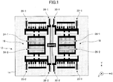
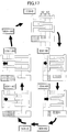
- FIG. 1 illustrates a configuration of a sensor 12 using a structure of a displacement amount monitoring electrode 10 according to a first embodiment of the present invention.
- the sensor 12 according to the present embodiment is an angular speed sensor installed in a vehicle, for example, for detecting the angular speed occurring around a Z-axis perpendicular to an X-Y plane.
- the sensor 12 is formed on a semiconductor substrate 14 made of, for example, silicon, and is formed by performing etching on the surface of the semiconductor substrate 14 by minute processing.
- the sensor 12 includes a pair of structure bodies 16, 18 being equal in mass, driving electrodes 20-1, 20-2, 22-1, 22-2 for exciting/driving the structure bodies 16, 18 in an X-axis direction on the semiconductor substrate 14, detection electrodes 24-1, 24-2, 26-1, 26-2 for detecting the oscillation (amplitude) in the Y-axis direction occurring in the structure bodies 16, 18 on the semiconductor substrate 14, and displacement amount monitoring electrodes 28-1, 28-2, 30-1, 30-2 for monitoring the drive displacement amount in the X-axis direction of the structure bodies 16, 18 on the semiconductor substrate 14.
- the structure bodies 16, 18 are disposed at mutually symmetrical positions on the semiconductor substrate 14 in a state where the structure bodies 16, 18 are lifted at a predetermined distance from the surface of the semiconductor substrate 14 forming an insulating layer.
- the displacement amount monitoring electrodes 28-1, 28-2, 30-1, 30-2 are referred to as the "displacement amount monitoring electrodes" 10 when referred to collectively.
- the driving electrodes 20-1, 20-2, 22-1, 22-2 and the detection electrodes 24-1, 24-2, 26-1, 26-2 are each constituted by a fixed electrode fixed to the semiconductor substrate 14 and a movable electrode movable in an X-axis direction or a Y-axis direction with respect to the semiconductor substrate 14. These fixed electrodes are connected to a signal processing circuit via a pad. Furthermore, these movable electrodes constitute a part of the structure bodies 16, 18.
- the driving electrodes 20-1, 20-2, 22-1, 22-2 are electrodes respectively for driving the structure bodies 16, 18 in the X-axis direction with respect to the semiconductor substrate 14, by activating an electrostatic attractive force between the fixed electrode and the movable electrode by applying a driving voltage to the fixed electrode.
- the detection electrodes 24-1, 24-2, 26-1, 26-2 are respectively electrodes for detecting the oscillation of the structure bodies 16, 18 in the Y-axis direction with respect to the semiconductor substrate 14, by detecting the change in the capacitance between the fixed electrode and the movable electrode caused by the displacement of the structure bodies 16, 18 in the Y-axis direction.
- a driving voltage which has substantially the same frequency as the resonance frequency of the structure bodies 16, 18, is applied to the fixed electrode from the signal processing circuit via a pad, so that an electrostatic attractive force is activated between the fixed electrode and the movable electrode, and a driving force is generated for exciting the structure bodies 16, 18 at a constant amplitude in the X-axis direction at a frequency substantially equal to the resonance frequency of the structure bodies 16, 18.
- the driving electrode 20-1 and the driving electrode 20-2 generate a driving force by the same phase and the driving electrode 22-1 and the driving electrode 22-2 generate a driving force by the same phase, while the driving electrodes 20-1, 20-2 and the driving electrodes 22-1, 22-2 generate a driving force by opposite phases.
- each of the detection electrodes 24-1, 24-2, 26-1, 26-2 a change in the capacitance occurs between the fixed electrode and the movable electrode, according to a displacement in the oscillation applied to the structure bodies 16, 18 in the Y-axis direction with respect to the semiconductor substrate 14.
- the change in the capacitance in the detection electrodes 24-1, 24-2 and the change in the capacitance in the detection electrodes 26-1, 26-2 are of opposite phases.
- the change in the capacitance of the detection electrodes 24-1, 24-2, 26-1, 26-2 is substantially zero when the oscillation displacement amount of the structure bodies 16, 18 in the Y-axis direction is zero, and increases as the oscillation displacement amount of the structure bodies 16, 18 in the Y-axis direction increases.
- the fixed electrode of each of the detection electrodes 24-1, 24-2, 26-1, 26-2 outputs, to the signal processing circuit, the change amount of the capacitance between the fixed electrode and the movable electrode, as a displacement detection signal.
- the signal processing circuit processes the displacement detection signal from each of the detection electrodes 24-1, 24-2, 26-1, 26-2 to detect the oscillation displacement amount of the structure bodies 16, 18 in the Y-axis direction, and detect the angular speed generated around the Z-axis based on the oscillation displacement amount.
- the driving electrodes 20-1, 20-2, 22-1, 22-2 are excited. Specifically, a driving voltage having a frequency that is substantially equal to the resonance frequency of the structure bodies 16, 18, is applied to the fixed electrode of the driving electrodes 20-1, 20-2, 22-1, 22-2.
- the detection electrodes 24-1, 24-2, 26-1, 26-2 are not oscillated/displaced in the Y-axis direction, and a change of the capacitance does not occur between the fixed electrode and the movable electrode of the detection electrodes 24-1, 24-2, 26-1, 26-2, and therefore the displacement detection signal output from the detection electrodes 24-1, 24-2, 26-1, 26-2 becomes a signal expressing that the amplitude of the structure bodies 16, 18 in the Y-axis direction is substantially zero.
- the detection electrodes 24-1, 24-2, 26-1, 26-2 are oscillated/displaced in the Y-axis direction according to the activation of the Coriolis force, and a change in the capacitance occurs between the fixed electrode and the movable electrode of the detection electrodes 24-1, 24-2, 26-1, 26-2.
- the displacement detection signal output from the detection electrodes 24-1, 24-2, 26-1, 26-2 becomes a signal expressing the extent of the angular speed of the amplitude generated at the structure bodies 16, 18 in the Y-axis direction.
- the structure bodies 16, 18 are oscillated/displaced in opposite phases with each other with respect to the Y-axis direction. Therefore, with the sensor 12, the angular speed occurring at the target around the Z-axis can be detected.
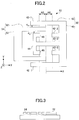
- FIG. 2 is a top view of the displacement amount monitoring electrode 10 according to the present embodiment.
- FIG. 3 is a cross-sectional view of the displacement amount monitoring electrode 10 according to the present embodiment.
- the displacement amount monitoring electrodes 10 as the displacement amount monitoring electrodes 28-1, 28-2, 30-1, 30-2 are each constituted by a fixed electrode 32 fixed to the semiconductor substrate 14 and a movable electrode 34 movable in the X-axis direction with respect to the semiconductor substrate 14.
- the fixed electrode 32 is connected to the signal processing circuit via a pad.
- the movable electrode 34 constitutes part of the structure bodies 16, 18.
- the displacement amount monitoring electrode 10 is an electrode for detecting the change in the capacitance between the fixed electrode 32 and the movable electrode 34 caused by the displacement of the structure bodies 16, 18 in the X-axis direction, to monitor the drive displacement amount (amplitude) of the structure bodies 16, 18 in the X-axis direction with respect to the semiconductor substrate 14.
- the fixed electrode 32 is formed to have a comb-teeth shape, and includes a base part 40 provided to have a relatively wide width, and electrode fingers 42 extending from the base part 40 in a stick-shape in an X-axis direction parallel to the semiconductor substrate 14.
- the base part 40 is formed to have a square cross-sectional shape, and is extending in a Y-axis direction parallel to the semiconductor substrate 14. Furthermore, there are a plurality of electrode fingers 42 arranged in a Y-axis direction parallel to each other, with respect to a single base part 40.
- the electrode fingers 42 include a long electrode finger 42-1 having a relatively long length in the X-axis direction, a short electrode finger 42-2 having a relatively short length in the X-axis direction, and a T-shaped electrode finger 42-3 having a relatively long length in the X-axis direction and whose leading end spreads out in the shape of wings in the Y-axis direction.
- Each of the long electrode finger 42-1 and the short electrode finger 42-2 of the electrode fingers 42 is formed to have a square cross-sectional shape and has the same cross-sectional area from the connection part with the base part 40 to the leading end (the same width in the Y-axis direction and the same thickness in the Z-axis direction). Furthermore, the T-shaped electrode finger 42-3 is formed to have a square cross-sectional shape and has the same cross-sectional area from the connection part with the base part 40 to a part near the leading end (the same width in the Y-axis direction and the same thickness in the Z-axis direction). The T-shaped electrode finger 42-3 has a leading end part 44 extending in the Y-axis direction.
- protrusion parts 46, 48 are provided, which extend in an X-axis direction parallel to the semiconductor substrate 14 from the leading end part 44 toward the base part 40 side. That is to say, the leading end part 44 is formed to have a U-shape as viewed from the top.
- the protrusion parts 46, 48 have the same cross-sectional area from the connection part with the leading end part 44 to the leading end (the same width in the Y-axis direction and the same thickness in the Z-axis direction), and have the same cross-sectional area as that of the short electrode finger 42-2 described above.
- the electrode fingers 42 are formed as a pattern in which one long electrode finger 42-1, two short electrode fingers 42-2, and one T-shaped electrode finger 42-3 constitute one set. Specifically, as illustrated in FIG. 2 , the long electrode finger 42-1, the short electrode finger 42-2, the T-shaped electrode finger 42-3, and the short electrode finger 42-2 are provided in the stated order in the Y-axis direction, and this configuration is repeated in the Y-axis direction.
- the electrode fingers 42 have a bilaterally symmetric configuration in which one of each of the short electrode finger 42-2 and the long electrode finger 42-1 are disposed in the stated order on either side of one T-shaped electrode finger 42-3.
- a predetermined gap is formed in the Y-axis direction between the long electrode finger 42-1 and the short electrode finger 42-2. Furthermore, a predetermined gap is formed in the Y-axis direction between the short electrode finger 42-2 and the T-shaped electrode finger 42-3. Note that the gap between the long electrode finger 42-1 and the short electrode finger 42-2, and the predetermined gap in the Y-axis direction between the short electrode finger 42-2 and the T-shaped electrode finger 42-3 may be different. Furthermore, the positions in the Y-axis direction of the protrusion parts 46, 48 of the leading end part 44 of the T-shaped electrode finger 42-3 are the same as the positions in the Y-axis direction of the short electrode fingers 42-2.
- the protrusion parts 46, 48 are disposed to be spaced apart by a predetermined distance in the X-axis direction from the short electrode fingers 42-2. Between the protrusion parts 46, 48 and the short electrode fingers 42-2, there is a predetermined gap formed in the X-axis direction.
- the protrusion parts 46, 48 and the short electrode fingers 42-2 constitute electrode fingers having cutouts which are holes formed by the predetermined gaps.
- the movable electrode 34 is formed to have a comb-teeth shape, and includes a base part 50 provided to have a relatively wide width, and electrode fingers 52 extending from the base part 50 in a stick-shape in an X-axis direction parallel to the semiconductor substrate 14.
- the base part 50 is formed to have a square cross-sectional shape, and is extending in a Y-axis direction parallel to the semiconductor substrate 14.
- each of the electrode fingers 52 is formed to have a square cross-sectional shape and has the same cross-sectional area from the connection part with the base part 50 to the leading end (the same width in the Y-axis direction and the same thickness in the Z-axis direction).
- the fixed electrode 32 and the movable electrode 34 are disposed such that the base parts 40, 50 face each other in the X-axis direction and the electrode fingers 42, 52 face each other and are meshed together in the Y-axis direction.
- the electrode fingers 52 of the movable electrode 34 are disposed so as to enter the center position in the Y-axis direction between the long electrode finger 42-1 and the short electrode finger 42-2 among the electrode fingers 42 of the fixed electrode 32.
- a predetermined gap d0 is formed in the Y-axis direction, between the electrode finger 52 of the movable electrode 34 and the long electrode finger 42-1 of the fixed electrode 32 adjacent to each other in the Y-axis direction, between the electrode finger 52 of the movable electrode 34 and the short electrode finger 42-2 of the fixed electrode 32 that may be adjacent to each other in the Y-axis direction, and between the electrode finger 52 of the movable electrode 34 and the protrusion parts 46, 48 of the leading end part 44 of the T-shaped electrode finger 42-3 of the fixed electrode 32 adjacent to each other in the Y-axis direction.
- the electrode fingers 52 of the movable electrode 34 are constituted such that the leading ends are positioned, in the X-axis direction, at the center of the gap between the leading ends of the protrusion parts 46, 48 of the fixed electrode 32 and the leading ends of the short electrode fingers 42-2, at the oscillation center (i.e., displacement center of the movable electrode 34) of the structure bodies 16, 18.
- the gap in the X-axis direction between the leading ends of the protrusion parts 46, 48 and the leading ends of the short electrode fingers 42-2 is set to be the same as a value that is two times a target amplitude (i.e., a target displacement amount from the oscillation center of the leading end of the movable electrode 34 corresponding to the target amplitude) A0 of the structure bodies 16, 18, or slightly smaller than this value.
- a target amplitude i.e., a target displacement amount from the oscillation center of the leading end of the movable electrode 34 corresponding to the target amplitude
- a thickness i.e., the height at a part where the side wall of the electrode fingers 42 and the side wall of the electrode fingers 52 face each other in the Z-axis direction
- the movable electrode 34 is displaced in the X-axis direction due to the excitation.
- a change in the capacitance occurs between the fixed electrode 32 and the movable electrode 34 due to the displacement of the movable electrode 34.
- the change in the capacitance at the displacement amount monitoring electrodes 28-1, 28-2 and the change in the capacitance at the displacement amount monitoring electrodes 30-1, 30-2 are of opposite phases from each other.
- the change in the capacitance of the displacement amount monitoring electrode 10 increases, as the driving displacement amount of the structure bodies 16, 18 in the X-axis direction increases.
- Each of the fixed electrodes of the displacement amount monitoring electrode 10 outputs, to the signal processing circuit, the change in the capacitance between the fixed electrode 32 and the movable electrode 34 as drive displacement amount monitor signals.
- the signal processing circuit monitors the drive displacement amount of the structure bodies 16, 18 in the X-axis direction by processing the drive displacement amount monitor signals from the displacement amount monitoring electrodes 10. Then, based on the drive displacement amount, the drive voltage to be applied to the driving electrodes 20-1, 20-2, 22-1, 22-2 is controlled so that the structure bodies 16, 18 are exited in the X-axis direction at a constant amplitude.
- the amplitude by which the structure bodies 16, 18 acting as a detection mass are exited in the X-axis direction need to be always maintained at a constant level.
- the capacitance change amount between the fixed electrode 32 and the movable electrode 34 of the displacement amount monitoring electrode 10 is generally maintained at a constant level.
- the driving voltage applied to the driving electrodes 20-1, 20-2 so that the capacitance change amount is maintained at a constant level; specifically, it is appropriate to perform drive control such that the drive displacement amount of the structure bodies 16, 18 reaches the target displacement amount (target amplitude) at the time point when the above capacitance change amount reaches the target capacitance change amount.
- FIG. 4 is a cross-sectional view of the displacement amount monitoring electrode 10 in the case where deformation has occurred due to stress changes.
- FIG. 5 illustrates the relationship (slope) between the drive displacement amount x of the structure bodies 16, 18, i.e., the movable electrode 34, that changes according to stress changes and size variations in the displacement amount monitoring electrode 10, and a capacitance change amount ⁇ C between the fixed electrode 32 and the movable electrode 34.
- the drive displacement amount x of the leading ends of the electrode fingers 52 of the movable electrode 34 is set as "0"
- the side to which the leading ends of the electrode fingers 52 come close to the base part 40 of the fixed electrode 32 is set as x >
- the side from which the leading ends of the electrode fingers 52 go away from the base part 40 of the fixed electrode 32 is set as x ⁇ 0.
- the capacitance change amount ⁇ C between the fixed electrode 32 and the movable electrode 34 does not only change according to the drive displacement amount x of the structure bodies 16, 18, but also changes according to the gap and the facing area between the fixed electrode 32 and the movable electrode 34. That is to say, the relationship between the drive displacement amount x and the capacitance change amount ⁇ C described above changes according to the gap and the facing area described above.
- the capacitance change amount ⁇ C between the fixed electrode 32 and the movable electrode 34 changes linearly with respect to the drive displacement amount x of the movable electrode 34.
- FIG. 6 illustrates the relationship between the drive displacement amount x of the structure bodies 16, 18, i.e., the movable electrode 34 and the capacitance change amount ⁇ C between the fixed electrode 32 and the movable electrode 34, in the displacement amount monitoring electrode 10 according to the present embodiment.
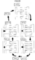
- FIG. 7 illustrates the operation procedures of the displacement amount monitoring electrode 10 according to the present embodiment.
- the capacitance change amount ⁇ C between the fixed electrode 32 and the movable electrode 34 is calculated according to the following formula (1). It is assumed that the vacuum dielectric constant is ⁇ 0, the relative permittivity of the space between the fixed electrode 32 and the movable electrode 34 is ⁇ r, the number of facing electrodes in the displacement amount monitoring electrode 10 is Nm, and the gap between the fixed electrode 32 and the movable electrode 34 in the Y-axis direction is dm.
- ⁇ C ⁇ 0 ⁇ ⁇ r ⁇ 2 ⁇ Tm ⁇ Nm ⁇ x / dm
- the electrode fingers 52 of the movable electrode 34 enters the center position in the Y-axis direction between the long electrode finger 42-1 and the short electrode finger 42-2 among the electrode fingers 42 of the fixed electrode 32, and the leading ends of the electrode fingers 52 are positioned, in the X-axis direction, at the center of the gap between the leading ends of the protrusion parts 46, 48 of the fixed electrode 32 and the leading ends of the short electrode fingers 42-2, at the oscillation center of the structure bodies 16, 18. Furthermore, between the electrode fingers 52 of the movable electrode 34 and the long electrode finger 42-1 of the electrode fingers 42 of the fixed electrode 32, a predetermined gap d0 is formed in the Y-axis direction.
- the gap between the leading ends of the protrusion parts 46, 48 of the fixed electrode 32 described above and the leading end of the short electrode finger 42-2 is set to be the same as a value that is two times a target amplitude A0 of the structure bodies 16, 18, or slightly smaller than this value.
- the long electrode finger 42-1 and the short electrode finger 42-2 among the electrode fingers 42 contribute to the increase in the facing area of the fixed electrode 32 and the movable electrode 34.
- the area where the fixed electrode 32 and the movable electrode 34 face each other with a gap d0 therebetween increases proportionally according to the displacement of the movable electrode 34, and also the increase in slope of the area is greater than the increase in slope in the first process described above. Therefore, in the second process described above, the capacitance change amount ⁇ C between the fixed electrode 32 and the movable electrode 34 increases by a greater slope compared to the slope of the first process described above.
- the long electrode finger 42-1 and the short electrode finger 42-2 among the electrode fingers 42 contribute to the decrease in the facing area of the fixed electrode 32 and the movable electrode 34.
- the area where the fixed electrode 32 and the movable electrode 34 face each other with a gap d0 therebetween decreases proportionally according to the displacement of the movable electrode 34. Therefore, in the third process described above, the capacitance change amount ⁇ C between the fixed electrode 32 and the movable electrode 34 decreases by the same slope as that of the second process described above.
- the area where the fixed electrode 32 and the movable electrode 34 face each other with a gap d0 therebetween decreases proportionally according to the displacement of the movable electrode 34, and the decrease in slope of the area is smaller than the decrease in slope of the third process described above. Therefore, in the fourth and fifth processes described above, the capacitance change amount ⁇ C between the fixed electrode 32 and the movable electrode 34 decreases by a smaller slope compared to the slope in the third process described above.
- the long electrode finger 42-1 and the protrusion parts 46, 48 of the T-shaped electrode fingers 42-3 among the electrode fingers 42 contribute to the decrease in the facing area of the fixed electrode 32 and the movable electrode 34.
- the area where the fixed electrode 32 and the movable electrode 34 face each other with a gap d0 therebetween decreases proportionally according to the displacement of the movable electrode 34, and also the decrease in slope of the area is greater than the decrease in slope in the fourth and fifth processes described above. Therefore, in the sixth process described above, the capacitance change amount ⁇ C between the fixed electrode 32 and the movable electrode 34 decreases by a greater slope compared to the slope of the fourth and fifth processes described above.
- the long electrode finger 42-1 and the short electrode finger 42-2 among the electrode fingers 42 contribute to the increase in the facing area of the fixed electrode 32 and the movable electrode 34.
- the area where the fixed electrode 32 and the movable electrode 34 face each other with a gap d0 therebetween increases proportionally according to the displacement of the movable electrode 34. Therefore, in the seventh process described above, the capacitance change amount ⁇ C between the fixed electrode 32 and the movable electrode 34 increases by the same slope as that of the sixth process described above.
- the capacitance change amount ⁇ C between the fixed electrode 32 and the movable electrode 34 increases by a smaller slope compared to the slope in the seventh process described above.
- the structure of the displacement amount monitoring electrode 10 has features that when the drive displacement amount x of the movable electrode 34 is between the target displacement amounts -AO and A0, the change sensitivity of the capacitance change amount ⁇ C between the fixed electrode 32 and the movable electrode 34 with respect to the drive displacement amount x of the movable electrode 34 in the X-axis direction is relatively small, while when the drive displacement amount x of the movable electrode 34 satisfies x ⁇ -A0 or x > A0, the change sensitivity is relatively large.
- the structure of the displacement amount monitoring electrode 10 has features that the change sensitivity of the capacitance change amount ⁇ C described above becomes higher after the drive displacement of the movable electrode 34 reaches the target displacement amount A0 compared to that before the drive displacement of the movable electrode 34 reaches the target displacement amount A0, and the change sensitivity becomes higher after the drive displacement of the movable electrode 34 reaches the target displacement amount -AO compared to that before the drive displacement of the movable electrode 34 reaches the target displacement amount -A0.
- the fixed electrode 32 and the movable electrode 34 are formed, such that the change sensitivity of the total area of the surfaces of the electrode fingers 42, 52 facing each other with a gap d0 therebetween becomes higher after the drive displacement of the movable electrode 34 reaches the target displacement amount A0 compared to that before the drive displacement of the movable electrode 34 reaches the target displacement amount A0, and the change sensitivity becomes higher after the drive displacement of the movable electrode 34 reaches the target displacement amount -AO compared to that before the drive displacement of the movable electrode 34 reaches the target displacement amount -A0.
- the fixed electrode 32 and the movable electrode 34 are formed, such that the number of parts where the electrode fingers 42, 52 face each other with a gap d0 therebetween increases after the drive displacement of the movable electrode 34 reaches the target displacement amount A0 compared to that before the drive displacement of the movable electrode 34 reaches the target displacement amount A0, and the number of the parts increases after the drive displacement of the movable electrode 34 reaches the target displacement amount -AO compared to that before the drive displacement of the movable electrode 34 reaches the target displacement amount -A0.
- the change sensitivity of the capacitance change amount ⁇ C between the fixed electrode 32 and the movable electrode 34 with respect to the drive displacement amount x of the movable electrode 34 after the movable electrode 34 is driven/displaced to the target displacement amount A0, -A0, is higher compared to that when the movable electrode 34 is positioned between the target displacement amounts - A0 and A0.
- the structure of the displacement amount monitoring electrode 10 of the present embodiment even when the relative relationship such as the gap and the facing area between the fixed electrode 32 and the movable electrode 34 changes, it is possible to prevent the drive displacement amount x of the movable electrode 34 from largely deviating from the target displacement amount A0 when the capacitance change amount ⁇ C reaches the target capacitance change amount C0. Therefore, it is possible to maintain the amplitude of the structure bodies 16, 18 to a constant target amplitude as much as possible. By this point, it is possible to increase the robustness with respect to disturbance factors such as assembly stress and temperature changes and manufacturing factors such as size variations, so that the yield can be improved and the ratio of nondefective products can be increased.
- the displacement amount monitoring electrode 10 in increasing the change sensitivity of the capacitance change amount ⁇ C between the fixed electrode 32 and the movable electrode 34 with respect to the drive displacement amount x of the movable electrode 34 after the movable electrode 34 is driven/displaced to the target displacement amount A0, -A0, it is unnecessary to reduce the gap between the leading ends of the electrode fingers 42 of the fixed electrode 32 and the movable electrode 34 and the base part 50, or the gap between the base part 40 and the leading ends of the electrode fingers 52, and a margin can be left in these gaps. Therefore, in the process of driving the structure bodies 16, 18 in the X-axis direction, the fixed electrode 32 and the movable electrode 34 can be prevented from colliding with each other, so that the displacement amount monitoring electrode 10 can be prevented from breaking.
- the structure bodies 16, 18 correspond to the "detection mass” in the claims, and the X direction corresponds to the "predetermined axis direction” in the claims.
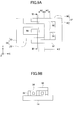
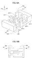
- the fixed electrode 32 includes the electrode fingers 42 that extend from the base part 40 in an X-axis direction parallel to the semiconductor substrate 14, and the electrode fingers 42 are constituted by three types of electrode fingers, the long electrode finger 42-1, the short electrode finger 42-2, and the T-shaped electrode finger 42-3; however, the present invention is not so limited. As illustrated in FIG. 8A and FIG.
- the fixed electrode 32 may include electrode fingers 80, 90 extending from the base part 40 in an X-axis direction parallel to the semiconductor substrate 14, and the electrode fingers 80, 90 may be constituted by two types of electrode fingers, i.e., long electrode fingers 82, 92 having a relatively long length in the X-axis direction and short electrode fingers 84, 94 having a relatively short length in the X-axis direction.
- the long electrode fingers 82, 92 and the short electrode fingers 84, 94 of the fixed electrode 32 are formed to have a square cross-sectional shape, and have the same cross-sectional area from the connection part with the base part 40 to the leading end (the same width in the Y-axis direction and the same thickness in the Z-axis direction).
- the electrode fingers 80, 90 are formed as a pattern in which one long electrode finger 82, 92 and one short electrode finger 84, 94 constitute one set. Specifically, the long electrode fingers 82, 92, and the short electrode fingers 84, 94 are provided in the stated order in the Y-axis direction, and this configuration is repeated in the Y-axis direction. In the electrode fingers 80, 90, a predetermined gap is formed in the Y-axis direction between the long electrode fingers 82, 92 and the short electrode fingers 84, 94.
- the fixed electrode 32 includes, as part of the electrode fingers 80, 90, separate parts 86, 96 that are not connected to the base part 40.
- the separate parts 86, 96 extend in an X-axis direction parallel to the semiconductor substrate 14 and are formed to have a square cross-sectional shape, and have the same cross-sectional shape between both ends in the X-axis direction (the same width in the Y-axis direction and the same thickness in the Z-axis direction).
- the positions of the separate parts 86, 96 in the Y-axis direction are the same as the positions of the short electrode fingers 84, 94 in the Y-axis direction.
- the separate parts 86, 96 are disposed to be spaced apart from the short electrode fingers 84, 94 by a predetermined distance in the X-axis direction. Between the separate parts 86, 96 and the short electrode fingers 84, 94, there is formed a predetermined gap in the X-axis direction.
- the separate parts 86, 96 and the short electrode fingers 84, 94 constitute electrode fingers including cutouts which are holes formed by the predetermined gaps.
- the separate part 86 may be maintained at the same potential as the other parts of the fixed electrode 32 (for example, the long electrode finger 82, the short electrode finger 84, etc.) by having the entire fixed electrode 32 electrically connected to the semiconductor substrate 14 as illustrated in FIG. 8B
- the separate part 96 may be maintained at the same potential as the other parts of the fixed electrode 32 (for example, the long electrode finger 92, the short electrode finger 94, etc.) by having the separate part 96 be electrically connected to the long electrode finger 92 via a top electrode 98 as illustrated in FIG. 9B .
- the fixed electrode 32 and the movable electrode 34 are disposed such that the base parts 40, 50 face each other in the X-axis direction and the electrode fingers 80, 90 and the electrode fingers 52 face each other and are meshed together in the Y-axis direction.
- the electrode fingers 52 of the movable electrode 34 are disposed so as to enter the center position in the Y-axis direction between the long electrode fingers 82, 92 and the short electrode fingers 84, 94 among the electrode fingers 80, 90 of the fixed electrode 32.
- a predetermined gap d0 is formed in the Y-axis direction, between the electrode finger 52 of the movable electrode 34 and the long electrode fingers 82, 92 of the fixed electrode 32 adjacent to each other in the Y-axis direction, between the electrode finger 52 of the movable electrode 34 and the short electrode fingers 84, 94 of the fixed electrode 32 that may be adjacent to each other in the Y-axis direction, and between the electrode finger 52 of the movable electrode 34 and the separate parts 86, 96 of the fixed electrode 32 adjacent to each other in the Y-axis direction.
- the electrode fingers 52 of the movable electrode 34 are constituted such that the leading ends are positioned, in the X-axis direction, at the center of the gap between one end of the separate parts 86, 96 of the fixed electrode 32 and the leading ends of the short electrode fingers 84, 94, at the oscillation center (i.e., displacement center of the movable electrode 34) of the structure bodies 16, 18.
- the gap in the X-axis direction between one end of the separate parts 86, 96 and the leading ends of the short electrode fingers 84, 94 is set to be the same as a value that is two times a target amplitude (i.e., a target displacement amount from the oscillation center of the leading end of the movable electrode 34 corresponding to the target oscillation) A0 of the structure bodies 16, 18, or slightly smaller than this value.
- a target amplitude i.e., a target displacement amount from the oscillation center of the leading end of the movable electrode 34 corresponding to the target oscillation
- a thickness i.e., the height at a part where the side wall of the electrode fingers 80, 90 and the side wall of the electrode fingers 52 face each other in the Z-axis direction
- the structure of the displacement amount monitoring electrode 10 according to the modification example also has features that when the drive displacement amount x of the movable electrode 34 is between the target displacement amounts -AO and A0, the change sensitivity of the capacitance change amount ⁇ C between the fixed electrode 32 and the movable electrode 34 with respect to the drive displacement amount x of the movable electrode 34 in the X-axis direction is relatively small, while when the drive displacement amount x of the movable electrode 34 satisfies x ⁇ -AO or x > A0, the change sensitivity is relatively large.
- the displacement amount monitoring electrode 10 has a feature that the change sensitivity of the capacitance change amount ⁇ C described above is larger after the drive displacement of the movable electrode 34 reaches the target displacement amount A0, -A0, compared to before the drive displacement reaches the target displacement amount A0, -A0.
- the fixed electrode 32 and the movable electrode 34 are formed such that the change sensitivity of the total area of the area where the electrode fingers 80, 90 and the electrode fingers 52 face each other with a gap d0 therebetween becomes larger after the drive displacement of the movable electrode 34 reaches the target displacement amount A0, -A0, compared to before the drive displacement reaches the target displacement amount A0, -A0; that is to say, the fixed electrode 32 is formed such that the number of parts where the electrode fingers 80, 90 and the electrode fingers 52 face each other with a gap d0 therebetween increases after the drive displacement of the movable electrode 34 reaches the target displacement amount A0, -A0, compared to that before the drive displacement of the movable electrode 34 reaches the target displacement amount A0, -A0. Therefore, also in the structure of this modification example, the same affects as the structure of the first embodiment described above can be attained.
- the gap where the electrode fingers 80, 90 of the fixed electrode 32 and the electrode fingers 52 of the movable electrode 34 face each other in the Y-axis direction can be at equal intervals at all parts, and therefore the configuration can be made compact compared to a structure in which the gap is unequal at the respective parts, and the area occupied by the displacement amount monitoring electrode 10 on the semiconductor substrate 14 can be prevented from increasing.
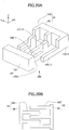
- FIG. 10 is a top view of a displacement amount monitoring electrode 100 according to a second embodiment of the present invention. Note that in FIG. 10 , the same elements as those of the configuration illustrated in FIG. 2 described above are denoted by the same reference numerals and descriptions thereof are omitted or simplified. Furthermore, FIG. 11 illustrates operation procedures in the displacement amount monitoring electrode 100 according to the present embodiment.
- the displacement amount monitoring electrode 100 includes the fixed electrode 32 and the movable electrode 34.
- the fixed electrode 32 is formed to have a comb-teeth shape, and includes electrode fingers 102 extending from the base part 40 in an X-axis direction parallel to the semiconductor substrate 14.
- the electrode fingers 102 have the same shape.
- Each of the electrode fingers 102 has a square cross-sectional shape, and is constituted so that the cross-sectional area changes from the connection part with the base part 40 to the leading end.
- the width in the Y-axis direction near the connection part with the base part 40 and at the part near the leading end is greater than the width in the Y-axis direction at a part in the middle of the these parts. Accordingly, the cross-sectional area near the connection part with the base part 40 and the part near the leading end is greater than the cross-sectional area at a part in the middle of the these parts.
- the part near the connection part with the base part 40 where the cross-sectional area is relatively large is referred to as a root part 102-1
- the part near the leading end where the cross-sectional area is relatively large is referred to as a leading end part 102-2
- the part in the middle where the cross-sectional area is relatively small is referred to as a middle part 102-3.
- the fixed electrode 32 and the movable electrode 34 are disposed such that the base parts 40, 50 face each other in the X-axis direction and the electrode fingers 102 and the electrode fingers 52 face each other and are meshed together in the Y-axis direction.
- the electrode fingers 52 of the movable electrode 34 are disposed so as to enter the center position between two electrode fingers 102 adjacent to each other in the Y-axis direction of the fixed electrode 32.
- the electrode fingers 52 of the movable electrode 34 and the electrode fingers 102 of the fixed electrode 32 adjacent to each other in the Y-axis direction are constituted so that different gaps dm are formed in the Y-axis direction according to the parts; specifically, the gap between the electrode finger 52 and the root part 102-1 and the gap between the electrode finger 52 and the leading end part 102-2 are relatively small, and the gap between the electrode finger 52 and the middle part 102-3 is relatively large.
- the electrode fingers 52 of the movable electrode 34 are constituted such that the leading ends are positioned, in the X-axis direction, at the center of the middle part 102-3 of the electrode fingers 102 of the fixed electrode 32 in the X-axis direction, at the oscillation center (i.e., displacement center of the movable electrode 34) of the structure bodies 16, 18.
- the length of the middle part 102-3 in the X-axis direction i.e., the distance in the X-axis direction between the root part 102-1 and the leading end part 102-2, is set to be the same as a value that is two times a target amplitude (i.e., a target displacement amount from the oscillation center of the leading end of the movable electrode 34 corresponding to the target amplitude) A0 of the structure bodies 16, 18, or slightly smaller than this value.
- a target amplitude i.e., a target displacement amount from the oscillation center of the leading end of the movable electrode 34 corresponding to the target amplitude
- a thickness i.e., the height at a part where the side wall of the electrode fingers 102 and the side wall of the electrode fingers 52 face each other in the Z-axis direction
- the middle part 102-3 among the electrode fingers 102 contributes to the increase in the facing area of the fixed electrode 32 and the movable electrode 34.
- the gap dm in the Y-axis direction between the electrode finger 102 of the fixed electrode 32 and the electrode finger 52 of the movable electrode 34 is a relatively large constant value. Therefore, in the above first process, the capacitance change amount ⁇ C between the fixed electrode 32 and the movable electrode 34 increases at a constant slope.
- the root part 102-1 among the electrode fingers 102 contributes to the increase in the facing area of the fixed electrode 32 and the movable electrode 34.
- the gap dm in the Y-axis direction between the electrode finger 102 of the fixed electrode 32 and the electrode finger 52 of the movable electrode 34 is a relatively small constant value. Therefore, in the second process described above, the capacitance change amount ⁇ C between the fixed electrode 32 and the movable electrode 34 increases by a greater slope compared to the slope of the first process described above.
- the root part 102-1 among the electrode fingers 102 contributes to the decrease in the facing area of the fixed electrode 32 and the movable electrode 34.
- the gap dm in the Y-axis direction between the electrode finger 102 of the fixed electrode 32 and the electrode finger 52 of the movable electrode 34 is a relatively small constant value. Therefore, in the third process described above, the capacitance change amount ⁇ C between the fixed electrode 32 and the movable electrode 34 decreases by the same slope as that of the second process described above.
- the middle part 102-3 among the electrode fingers 102 contributes to the decrease in the facing area of the fixed electrode 32 and the movable electrode 34.
- the gap dm in the Y-axis direction between the electrode finger 102 of the fixed electrode 32 and the electrode finger 52 of the movable electrode 34 is a relatively large constant value. Therefore, in the fourth and fifth processes described above, the capacitance change amount ⁇ C between the fixed electrode 32 and the movable electrode 34 decreases by a smaller slope compared to the slope in the third process described above.
- the leading end part 102-2 among the electrode fingers 102 contributes to the decrease in the facing area of the fixed electrode 32 and the movable electrode 34.
- the gap dm in the Y-axis direction between the electrode finger 102 of the fixed electrode 32 and the electrode finger 52 of the movable electrode 34 is a relatively small constant value. Therefore, in the sixth process described above, the capacitance change amount ⁇ C between the fixed electrode 32 and the movable electrode 34 decreases by a greater slope compared to the slope of the fourth and fifth processes described above.
- the leading end part 102-2 among the electrode fingers 102 contributes to the increase in the facing area of the fixed electrode 32 and the movable electrode 34.
- the gap dm in the Y-axis direction between the electrode finger 102 of the fixed electrode 32 and the electrode finger 52 of the movable electrode 34 is a relatively small constant value. Therefore, in the seventh processes described above, the capacitance change amount ⁇ C between the fixed electrode 32 and the movable electrode 34 increases by the same slope as that of the sixth process described above.
- the middle part 102-3 among the electrode fingers 102 contributes to the increase in the facing area of the fixed electrode 32 and the movable electrode 34.
- the gap dm in the Y-axis direction between the electrode finger 102 of the fixed electrode 32 and the electrode finger 52 of the movable electrode 34 is a relatively large constant value. Therefore, in the eighth process described above, the capacitance change amount ⁇ C between the fixed electrode 32 and the movable electrode 34 increases by a smaller slope compared to the slope in the seventh process described above.
- the structure of the displacement amount monitoring electrode 100 also has features that when the drive displacement amount x of the movable electrode 34 is between the target displacement amounts -AO and A0, the change sensitivity of the capacitance change amount ⁇ C between the fixed electrode 32 and the movable electrode 34 with respect to the drive displacement amount x of the movable electrode 34 in the X-axis direction is relatively small, while when the drive displacement amount x of the movable electrode 34 satisfies x ⁇ -AO or x > A0, the change sensitivity is relatively large.
- the structure of the displacement amount monitoring electrode 100 has features that the change sensitivity of the capacitance change amount ⁇ C described above becomes higher after the drive displacement of the movable electrode 34 reaches the target displacement amount A0 compared to that before the drive displacement of the movable electrode 34 reaches the target displacement amount A0, and the change sensitivity becomes higher after the drive displacement of the movable electrode 34 reaches the target displacement amount -AO compared to that before the drive displacement of the movable electrode 34 reaches the target displacement amount -A0.
- the fixed electrode 32 and the movable electrode 34 are formed, such that the gap dm where the electrode fingers 102, 52 face each other (particularly, the gap where the leading end of the electrode finger 52 faces the electrode finger 102) becomes smaller after the drive displacement of the movable electrode 34 reaches the target displacement amount A0 compared to that before the drive displacement of the movable electrode 34 reaches the target displacement amount A0, and the change sensitivity becomes smaller after the drive displacement of the movable electrode 34 reaches the target displacement amount -AO compared to that before the drive displacement of the movable electrode 34 reaches the target displacement amount -A0.
- the change sensitivity of the capacitance change amount ⁇ C between the fixed electrode 32 and the movable electrode 34 with respect to the drive displacement amount x of the movable electrode 34 after the movable electrode 34 is driven/displaced to the target displacement amount A0, -A0 is higher compared to that when the movable electrode 34 is positioned between the target displacement amounts - A0 and A0. Therefore, also in the structure of the displacement amount monitoring electrode 100 according to the present embodiment, the same effects as those of the structure of the displacement amount monitoring electrode 10 according to the first embodiment can be achieved.
- the gap where the respective parts of the electrode fingers 102 of the fixed electrode 32 and the electrode fingers 52 of the movable electrode 34 are adjacent to each other in the Y-axis direction, and the gap where the respective parts of the electrode fingers 102 of the fixed electrode 32 are adjacent to each other in the Y-axis direction can be at equal intervals, and therefore the configuration can be simplified and made compact compared to a structure having unequal gaps.
- the gap dm where the electrode fingers 102, 52 of the fixed electrode 32 and the movable electrode 34 face each other is made smaller after the drive displacement of the movable electrode 34 reaches the target displacement amount A0 compared to that before the drive displacement of the movable electrode 34 reaches the target displacement amount A0.
- the electrode finger 52 of the movable electrode 34 has the same cross-sectional area from the connection part with the base part 50 to the leading end
- the electrode finger 102 of the fixed electrode 32 has a cross-sectional area that changes from the connection part with the base part 40 to the leading end.
- the electrode fingers of the fixed electrode 32 and the electrode fingers of the movable electrode 34 may respectively have a cross-sectional area that changes from the connection part with the base part to the leading end.
- each electrode finger 120 of the fixed electrode 32 may be constituted by a root part 120-1 near the connection part with the base part 40 where the cross-sectional area is relatively large, a leading end part 120-2 near the leading end where the cross-sectional area is relatively large, and a middle part 120-3 where the cross-sectional area is relatively small; and each electrode finger 122 of the movable electrode 34 may be constituted by a root part 122-1 near the connection part with the base part 50 where the cross-sectional area is relatively large, a leading end part 122-2 near the leading end where the cross-sectional area is relatively large, and a middle part 122-3 where the cross-sectional area is relatively small.
- the change sensitivity of the capacitance change amount ⁇ C between the fixed electrode 32 and the movable electrode 34 becomes even higher after the drive displacement of the movable electrode 34 reaches the target displacement amount A0, -AO compared to that before the drive displacement of the movable electrode 34 reaches the target displacement amount A0, -A0, and therefore the effects can be made even more significant compared to that of the second embodiment described above.
- each electrode finger 130 of the fixed electrode 32 may be constituted by a root part 130-1 near the connection part with the base part 40 where the cross-sectional area is relatively large, and a foundation part 130-2 where the cross-sectional area is relatively small; and each electrode finger 132 of the movable electrode 34 may be constituted by a root part 132-1 near the connection part with the base part 50 where the cross-sectional area is relatively large, a leading end part 132-2 near the leading end where the cross-sectional area is relatively large, and a middle part 132-3 where the cross-sectional area is relatively small.
- the change sensitivity of the capacitance change amount ⁇ C between the fixed electrode 32 and the movable electrode 34 becomes even higher after the drive displacement of the movable electrode 34 reaches the target displacement amount A0 compared to that before the drive displacement of the movable electrode 34 reaches the target displacement amount A0, and therefore the effects can be made even more significant compared to that of the second embodiment described above.
- each electrode finger 140 of the fixed electrode 32 may be constituted by a root part 140-1 near the connection part with the base part 40 where the cross-sectional area is relatively large, and a foundation part 140-2 where the cross-sectional area is relatively small; and each electrode finger 142 of the movable electrode 34 may be constituted by a foundation part 142-1 where the cross-sectional area is relatively small and a leading end part 142-2 near the connection part with the base part 50 where the cross-sectional area is relatively large.
- the change sensitivity of the capacitance change amount ⁇ C between the fixed electrode 32 and the movable electrode 34 becomes even higher after the drive displacement of the movable electrode 34 reaches the target displacement amount A0 compared to that before the drive displacement of the movable electrode 34 reaches the target displacement amount A0, and therefore the effects can be made even more significant compared to that of the second embodiment described above.
- the gaps at the respective parts where the electrode fingers of the fixed electrode 32 and the electrode fingers of the movable electrode 34 face each other in the Y-axis direction, and the gaps at the respective parts where the electrode fingers of the fixed electrode 32 are adjacent to each other in the Y-axis direction, can be can be at equal intervals (that is to say, as illustrated in FIG.
- FIG. 16 is a top view of a displacement amount monitoring electrode 200 according to a third embodiment of the present invention. Note that in FIG. 16 , the same elements as those of the configuration illustrated in FIG. 2 described above are denoted by the same reference numerals and descriptions thereof are omitted or simplified. Furthermore, FIG. 17 illustrates operation procedures in the displacement amount monitoring electrode 200 according to the present embodiment.
- the displacement amount monitoring electrode 200 includes the fixed electrode 32 and the movable electrode 34.
- the fixed electrode 32 is formed to have a comb-teeth shape, and includes electrode fingers 202 extending from the base part 40 in an X-axis direction parallel to the semiconductor substrate 14.
- the electrode fingers 202 have the same shape.
- Each of the electrode fingers 202 has a square cross-sectional shape, and is constituted so that the cross-sectional area changes from the connection part with the base part 40 to the leading end.
- the thickness in the Z-axis direction near the connection part with the base part 40 and at the part near the leading end is greater than the thickness in the Z-axis direction at a part in the middle of the these parts. Accordingly, the cross-sectional area at the part near the connection part with the base part 40 and the part near the leading end is greater than the cross-sectional area at a part in the middle of the these parts.
- the part near the connection part with the base part 40 where the cross-sectional area is relatively large is referred to as a root part 202-1
- the part near the leading end where the cross-sectional area is relatively large is referred to as a leading end part 202-2
- the part in the middle where the cross-sectional area is relatively small is referred to as a middle part 202-3.
- the fixed electrode 32 and the movable electrode 34 are disposed such that the base parts 40, 50 face each other in the X-axis direction and the electrode fingers 202 and the electrode fingers 52 face each other and are meshed together in the Y-axis direction.
- the electrode fingers 52 of the movable electrode 34 are disposed so as to enter the center position between two electrode fingers 202 adjacent to each other in the Y-axis direction of the fixed electrode 32.
- a predetermined gap d0 is formed in the Y-axis direction.
- the electrode fingers 52 of the movable electrode 34 are constituted such that the leading ends are positioned, in the X-axis direction, at the center of the middle part 202-3 of the electrode finger 202 of the fixed electrode 32, at the oscillation center (i.e., displacement center of the movable electrode 34) of the structure bodies 16, 18.
- the distance in the X-axis direction of the middle part 202-3 is set to be the same as a value that is two times a target amplitude (i.e., a target displacement amount from the oscillation center of the leading end of the movable electrode 34 corresponding to the target amplitude) A0 of the structure bodies 16, 18, or slightly smaller than this value.
- a target amplitude i.e., a target displacement amount from the oscillation center of the leading end of the movable electrode 34 corresponding to the target amplitude
- a thickness (i.e., the height at a part where the side wall of the electrode fingers 202 and the side wall of the electrode fingers 52 face each other in the Z-axis direction) Tm at a part where the electrode fingers 202 of the fixed electrode 32 and the electrode fingers 52 of the movable electrode 34 adjacent to each other in the Y-axis direction overlap in the thickness direction, i.e., the Z-axis direction, is set to be different according to the parts; specifically, the thickness between the electrode finger 52 and the root part 202-1 and the thickness between the electrode finger 52 and the leading end part 202-2 are relatively large, and the thickness between the electrode finger 52 and the middle part 202-3 is relatively small.
- the middle part 202-3 among the electrode fingers 202 contributes to the increase in the facing area of the fixed electrode 32 and the movable electrode 34.
- the height Tm in the Z-axis direction where the electrode finger 202 of the fixed electrode 32 and the electrode finger 52 of the movable electrode 34 face each other in the Y-axis direction is a relatively small constant value, and the area where the fixed electrode 32 and the movable electrode 34 face each other with a gap d0 therebetween, increases proportionally according to the displacement of the movable electrode 34. Therefore, in the above first process, the capacitance change amount ⁇ C between the fixed electrode 32 and the movable electrode 34 increases at a constant slope.
- the root part 202-1 among the electrode fingers 202 contributes to the increase in the facing area of the fixed electrode 32 and the movable electrode 34.
- the height Tm in the Z-axis direction where the electrode finger 202 of the fixed electrode 32 and the electrode finger 52 of the movable electrode 34 face each other in the Y-axis direction is a relatively large constant value, and the area where the fixed electrode 32 and the movable electrode 34 face each other with a gap d0 therebetween, increases proportionally according to the displacement of the movable electrode 34, and also the increase in slope of the area is greater than the increase in slope in the first process described above. Therefore, in the second process described above, the capacitance change amount ⁇ C between the fixed electrode 32 and the movable electrode 34 increases by a greater slope compared to the slope of the first process described above.
- the root part 202-1 among the electrode fingers 202 contributes to the decrease in the facing area of the fixed electrode 32 and the movable electrode 34.
- the height Tm in the Z-axis direction where the electrode finger 202 of the fixed electrode 32 and the electrode finger 52 of the movable electrode 34 face each other in the Y-axis direction is a relatively large constant value, and the area where the fixed electrode 32 and the movable electrode 34 face each other with a gap d0 therebetween, decreases proportionally according to the displacement of the movable electrode 34. Therefore, in the third process described above, the capacitance change amount ⁇ C between the fixed electrode 32 and the movable electrode 34 decreases by the same slope as that of the second process described above.
- the middle part 202-3 among the electrode fingers 202 contributes to the decrease in the facing area of the fixed electrode 32 and the movable electrode 34.
- the height Tm in the Z-axis direction where the electrode finger 202 of the fixed electrode 32 and the electrode finger 52 of the movable electrode 34 face each other in the Y-axis direction is a relatively small constant value, and the area where the fixed electrode 32 and the movable electrode 34 face each other with a gap d0 therebetween, decreases proportionally according to the displacement of the movable electrode 34, and also the decrease in slope of the area is smaller than the decrease in slope in the third process described above. Therefore, in the fourth and fifth processes described above, the capacitance change amount ⁇ C between the fixed electrode 32 and the movable electrode 34 decreases by a smaller slope compared to the slope in the third process described above.
- the leading end part 202-2 among the electrode fingers 202 contributes to the decrease in the facing area of the fixed electrode 32 and the movable electrode 34.
- the height Tm in the Z-axis direction where the electrode finger 202 of the fixed electrode 32 and the electrode finger 52 of the movable electrode 34 face each other in the Y-axis direction is a relatively large constant value, and the area where the fixed electrode 32 and the movable electrode 34 face each other with a gap d0 therebetween, decreases proportionally according to the displacement of the movable electrode 34, and also the decrease in slope of the area is greater than the decrease in slope in the fourth and fifth processes described above. Therefore, in the sixth process described above, the capacitance change amount ⁇ C between the fixed electrode 32 and the movable electrode 34 decreases by a greater slope compared to the slope of the fourth and fifth processes described above.
- the leading end part 202-2 among the electrode fingers 202 contributes to the increase in the facing area of the fixed electrode 32 and the movable electrode 34.
- the height Tm in the Z-axis direction where the electrode finger 202 of the fixed electrode 32 and the electrode finger 52 of the movable electrode 34 face each other in the Y-axis direction is a relatively large constant value, and the area where the fixed electrode 32 and the movable electrode 34 face each other with a gap d0 therebetween, increases proportionally according to the displacement of the movable electrode 34. Therefore, in the seventh processes described above, the capacitance change amount ⁇ C between the fixed electrode 32 and the movable electrode 34 increases by the same slope as that of the sixth process described above.
- the middle part 202-3 among the electrode fingers 202 contributes to the increase in the facing area of the fixed electrode 32 and the movable electrode 34.
- the height Tm in the Z-axis direction where the electrode finger 202 of the fixed electrode 32 and the electrode finger 52 of the movable electrode 34 face each other in the Y-axis direction is a relatively small constant value, and the area where the fixed electrode 32 and the movable electrode 34 face each other with a gap d0 therebetween, increases proportionally according to the displacement of the movable electrode 34, and also the increase in slope of the area is smaller than the increase in slope in the seventh process described above. Therefore, in the eighth process described above, the capacitance change amount ⁇ C between the fixed electrode 32 and the movable electrode 34 increases by a smaller slope compared to the slope in the seventh process described above.
- the structure of the displacement amount monitoring electrode 200 also has features that when the drive displacement amount x of the movable electrode 34 is between the target displacement amounts -A0 and A0, the change sensitivity of the capacitance change amount ⁇ C between the fixed electrode 32 and the movable electrode 34 with respect to the drive displacement amount x of the movable electrode 34 in the X-axis direction is relatively small, while when the drive displacement amount x of the movable electrode 34 satisfies x ⁇ -A0 or x > A0, the change sensitivity is relatively large.
- the structure of the displacement amount monitoring electrode 200 has features that the change sensitivity of the capacitance change amount ⁇ C described above becomes higher after the drive displacement of the movable electrode 34 reaches the target displacement amount A0 compared to that before the drive displacement of the movable electrode 34 reaches the target displacement amount A0, and the change sensitivity becomes higher after the drive displacement of the movable electrode 34 reaches the target displacement amount -A0 compared to that before the drive displacement of the movable electrode 34 reaches the target displacement amount -A0.
- the fixed electrode 32 and the movable electrode 34 are formed, such that the height Tm in the Z-axis direction where the electrode fingers 202, 52 face each other in the Y-axis direction (particularly, the height in the Z-axis direction where the leading end of the electrode finger 52 faces the electrode finger 202) becomes higher after the drive displacement of the movable electrode 34 reaches the target displacement amount A0 compared to that before the drive displacement of the movable electrode 34 reaches the target displacement amount A0, and the change sensitivity becomes higher after the drive displacement of the movable electrode 34 reaches the target displacement amount -A0 compared to that before the drive displacement of the movable electrode 34 reaches the target displacement amount -A0.
- the change sensitivity of the capacitance change amount ⁇ C between the fixed electrode 32 and the movable electrode 34 with respect to the drive displacement amount x of the movable electrode 34 after the movable electrode 34 is driven/displaced to the target displacement amounts A0, -A0 is higher compared to that when the movable electrode 34 is positioned between the target displacement amounts - A0 and A0. Therefore, also in the structure of the displacement amount monitoring electrode 200 according to the present embodiment, the same effects as those of the structure of the displacement amount monitoring electrode 10, 100 according to the first embodiment and the second embodiment can be achieved.
- the electrode finger 202 of the fixed electrode 32 and the electrode finger 52 of the movable electrode 34 each has a width in the Y-axis direction that does not change from the leading end to the connection part with the base part 40, 50.
- the gap where the electrode finger 202 of the fixed electrode 32 and the electrode finger 52 of the movable electrode 34 face each other in the Y-axis direction, the gap where the electrode fingers 202 of the fixed electrode 32 are adjacent to each other in the Y-axis direction, and the gap where the electrode fingers 52 of the movable electrode 34 are adjacent to each other in the Y-axis direction, can have a minimum length and can be at equal intervals, and therefore the configuration can be simplified and made compact compared to a structure having unequal gaps, and the area occupied by the displacement amount monitoring electrode 200 on the semiconductor substrate 14 can be prevented from increasing.
- the height Tm in the Z-axis direction where the electrode fingers 202, 52 of the fixed electrode 32 and the movable electrode 34 face each other in the Y-axis direction is made smaller after the drive displacement of the movable electrode 34 reaches the target displacement amount A0 compared to that before the drive displacement of the movable electrode 34 reaches the target displacement amount A0.
- the electrode fingers 52 of the movable electrode 34 is made to have the same cross-sectional area from the connection part with the base part 50 to the leading end, and the electrode finger 202 of the fixed electrode 32 has a cross-sectional area that changes from the connection part with the base part 40 to the leading end.
- the present invention is not so limited.
- the electrode fingers of the fixed electrode 32 and the electrode fingers of the movable electrode 34 may respectively have a cross-sectional area that changes from the connection part with the base part to the leading end.
- each electrode finger 220 of the fixed electrode 32 may be constituted by a root part 220-1 near the connection part with the base part 40 where the cross-sectional area is relatively large, a leading end part 220-2 near the leading end where the cross-sectional area is relatively large, and a middle part 220-3 where the cross-sectional area is relatively small; and each electrode finger 222 of the movable electrode 34 may be constituted by a root part 222-1 near the connection part with the base part 50 where the cross-sectional area is relatively large, a leading end part 222-2 near the leading end where the cross-sectional area is relatively large, and a middle part 222-3 where the cross-sectional area is relatively small.
- the change sensitivity of the capacitance change amount ⁇ C between the fixed electrode 32 and the movable electrode 34 becomes even higher after the drive displacement of the movable electrode 34 reaches the target displacement amount A0, -A0 compared to that before the drive displacement of the movable electrode 34 reaches the target displacement amount A0, -A0, and therefore the effects can be made even more significant compared to that of the third embodiment described above.
- each electrode finger 230 of the fixed electrode 32 may be constituted by a root part 230-1 near the connection part with the base part 40 where the cross-sectional area is relatively large, and a foundation part 230-2 where the cross-sectional area is relatively small; and each electrode finger 232 of the movable electrode 34 may be constituted by a root part 232-1 near the connection part with the base part 50 where the cross-sectional area is relatively large, a leading end part 232-2 near the leading end where the cross-sectional area is relatively large, and a middle part 232-3 where the cross-sectional area is relatively small.
- the change sensitivity of the capacitance change amount ⁇ C between the fixed electrode 32 and the movable electrode 34 becomes even higher after the drive displacement of the movable electrode 34 reaches the target displacement amount A0 compared to that before the drive displacement of the movable electrode 34 reaches the target displacement amount A0, and therefore the effects can be made even more significant compared to that of the third embodiment described above.
- each electrode finger 240 of the fixed electrode 32 may be constituted by a root part 240-1 near the connection part with the base part 40 where the cross-sectional area is relatively large, and a foundation part 240-2 where the cross-sectional area is relatively small; and each electrode finger 242 of the movable electrode 34 may be constituted by a foundation part 242-1 where the cross-sectional area is relatively small and a leading end part 242-2 near the connection part with the base part 50 where the cross-sectional area is relatively large.
- the change sensitivity of the capacitance change amount ⁇ C between the fixed electrode 32 and the movable electrode 34 becomes even higher after the drive displacement of the movable electrode 34 reaches the target displacement amount A0 compared to that before the drive displacement of the movable electrode 34 reaches the target displacement amount A0, and therefore the effects can be made even more significant compared to that of the third embodiment described above.
- the gap where the electrode finger of the fixed electrode 32 and the electrode finger of the movable electrode 34 face each other in the Y-axis direction can have a minimum length and can be at equal intervals (for example, as illustrated in FIG.
- FIG. 22A is a top view of a displacement amount monitoring electrode 300 according to a fourth embodiment of the present invention.
- FIG. 22B is a cross-sectional view cut along V-V of the displacement amount monitoring electrode 300 illustrated in FIG. 22A .
- FIG. 22A and FIG. 22B the same elements as those of the configuration illustrated in FIG. 2 described above are denoted by the same reference numerals and descriptions thereof are omitted or simplified.
- FIG. 23 illustrates operation procedures in the displacement amount monitoring electrode 300 according to the present embodiment.
- the displacement amount monitoring electrode 300 includes the fixed electrode 32 and the movable electrode 34.
- the fixed electrode 32 is formed to have a comb-teeth shape, and includes electrode fingers 302 extending from the base part 40 in an X-axis direction parallel to the semiconductor substrate 14.
- the electrode fingers 302 have the same shape.
- Each of the electrode fingers 302 has a square cross-sectional shape, and has the same cross-sectional area from the connection part with the base part 40 to the leading end (the same width in the Y-axis direction and the same thickness in the Z-axis direction).
- a thickness i.e., the height at a part where the side wall of the electrode fingers 302 and the side wall of the electrode fingers 52 face each other in the Z-axis direction
- Tm a thickness at a part where the electrode fingers 302 and the electrode fingers 52 of the movable electrode 34 overlap in the thickness direction, i.e., the Z-axis direction
- dielectric materials 304, 306 are disposed at the electrode fingers 302 of the fixed electrode 32.
- the dielectric materials 304, 306 are disposed on both of the side faces of the electrode finger 302 facing the electrode fingers 52 of the movable electrode 34 in the Y-axis direction.
- the dielectric materials 304, 306 are constituted by a material having high insulation properties or a material having a low Young's modulus or having viscosity, which is different from the material of the main body of the electrode finger 302.
- the dielectric materials 304, 306 have a relative permittivity that is higher than the relative permittivity of air "1", and have a predetermined thickness d 1 in the Y-axis direction on the surface of the electrode finger 302.
- the dielectric materials 304, 306 may be manufactured by using an organic material such as, for example, a SiO2 film (oxide insulating film) that can be easily deposited by thermally oxidizing silicon, or a resist material.
- an organic material such as, for example, a SiO2 film (oxide insulating film) that can be easily deposited by thermally oxidizing silicon, or a resist material.
- the part near the connection part with the base part 40 where the dielectric material 304 is provided is referred to as a root part 302-1
- the part near the leading end where the dielectric material 306 is provided is referred to as a leading end part 302-2
- the part in the middle of the root part 302-1 and the leading end part 302-2 is referred to as a middle part 302-3.
- the fixed electrode 32 and the movable electrode 34 are disposed such that the base parts 40, 50 face each other in the X-axis direction and the electrode fingers 302 and the electrode fingers 52 face each other and are meshed together in the Y-axis direction.
- the electrode fingers 52 of the movable electrode 34 are disposed so as to enter the center position between two electrode fingers 302 adjacent to each other in the Y-axis direction of the fixed electrode 32.
- a predetermined gap d 0 is formed in the Y-axis direction at the middle part 302-3 of the electrode finger 302, and a predetermined gap (d 0 -d 1 ) is formed in the Y-axis direction at the root part 302-1 and the leading end part 302-2.
- the electrode fingers 52 of the movable electrode 34 are constituted such that the leading ends are positioned, in the X-axis direction, at the center of the middle part 302-3 of the electrode finger 302 of the fixed electrode 32, at the oscillation center (i.e., displacement center of the movable electrode 34) of the structure bodies 16, 18.
- the length of the middle part 302-3 in the X-axis direction i.e., the distance in the X-axis direction between the root part 302-1 and the leading end part 302-2 (the distance of the space between one end of the dielectric material 304 and one end of the dielectric material 306 in the X-axis direction) is set to be the same as a value that is two times a target amplitude (i.e., a target displacement amount from the oscillation center of the leading end of the movable electrode 34 corresponding to the target amplitude) A0 of the structure bodies 16, 18, or slightly smaller than this value.
- a target amplitude i.e., a target displacement amount from the oscillation center of the leading end of the movable electrode 34 corresponding to the target amplitude
- a thickness i.e., the height at a part where the side wall of the electrode fingers 302 and the side wall of the electrode fingers 52 face each other in the Z-axis direction
- the middle part 302-3 among the electrode fingers 302 contributes to the increase in the facing area of the fixed electrode 32 and the movable electrode 34.
- the change amount of the facing area where the fixed electrode 32 and the movable electrode 34 face each other is ⁇ S.
- ⁇ C 1 ⁇ 1 ⁇ ⁇ S / d 0
- the root part 302-1 among the electrode fingers 302 contributes to the increase in the facing area of the fixed electrode 32 and the movable electrode 34.
- the capacitance change amount ⁇ C2 between the fixed electrode 32 and the movable electrode 34 is based on the capacitance change amount of the dielectric material 304 and the capacitance change amount of the space between the dielectric material 304 and the electrode finger 52 of the movable electrode 34 in the Y-axis direction, as indicated in the following formula (3), and the capacitance change amount ⁇ C2 increases by a larger slope compared to the slope of the first process described above, according to the drive displacement amount x described above.
- the dielectric constant of the space between the electrode finger 302 of the fixed electrode 32 and the electrode finger 52 of the movable electrode 34 is ⁇ 1
- the dielectric constant of the dielectric material 304 is ⁇ 2(> ⁇ 1)
- the change amount of the facing area of the fixed electrode 32 and the movable electrode 34 is ⁇ S.
- ⁇ C 2 ⁇ 1 ⁇ ⁇ 2 ⁇ ⁇ S / ⁇ 2 ⁇ d 0 ⁇ d 1 + ⁇ 1 ⁇ d 1
- the root part 302-1 among the electrode fingers 302 contributes to the decrease in the facing area of the fixed electrode 32 and the movable electrode 34. Therefore, in the third process described above, the capacitance change amount ⁇ C between the fixed electrode 32 and the movable electrode 34 decreases by the same slope as the slope of the second process described above, according to the drive displacement amount x described above.
- the middle part 302-3 among the electrode fingers 302 contributes to the decrease in the facing area of the fixed electrode 32 and the movable electrode 34. Therefore, in the fourth and fifth processes described above, the capacitance change amount ⁇ C between the fixed electrode 32 and the movable electrode 34 decreases by a smaller slope compared to the slope of the third process described above, according to the drive displacement amount x described above.
- the leading end part 302-2 among the electrode fingers 302 contributes to the decrease in the facing area of the fixed electrode 32 and the movable electrode 34.
- the capacitance change amount ⁇ C between the fixed electrode 32 and the movable electrode 34 is based on the capacitance change amount of the dielectric material 306, and the capacitance change amount of the space between the dielectric material 306 and the electrode finger 52 of the movable electrode 34, and decreases by a larger slope compared to the slope of the fourth and fifth processes described above, according to the drive displacement amount x described above.
- the leading end part 302-2 among the electrode fingers 302 contributes to the increase in the facing area of the fixed electrode 32 and the movable electrode 34. Therefore, in the seventh process described above, the capacitance change amount ⁇ C between the fixed electrode 32 and the movable electrode 34 increases by the same slope as the slope of the sixth process described above, according to the drive displacement amount x described above.
- the middle part 302-3 among the electrode fingers 302 contributes to the increase in the facing area of the fixed electrode 32 and the movable electrode 34. Therefore, in the eighth process described above, the capacitance change amount ⁇ C between the fixed electrode 32 and the movable electrode 34 increases by a smaller slope compared to the slope of the seventh process described above, according to the drive displacement amount x described above.
- the structure of the displacement amount monitoring electrode 300 also has features that when the drive displacement amount x of the movable electrode 34 is between the target displacement amounts -A0 and A0, the change sensitivity of the capacitance change amount ⁇ C between the fixed electrode 32 and the movable electrode 34 with respect to the drive displacement amount x of the movable electrode 34 in the X-axis direction is relatively small, while when the drive displacement amount x of the movable electrode 34 satisfies x ⁇ -A0 or x > A0, the change sensitivity is relatively large.
- the structure of the displacement amount monitoring electrode 300 has features that the change sensitivity of the capacitance change amount ⁇ C described above becomes higher after the drive displacement of the movable electrode 34 reaches the target displacement amount A0 compared to that before the drive displacement of the movable electrode 34 reaches the target displacement amount A0, and the change sensitivity becomes higher after the drive displacement of the movable electrode 34 reaches the target displacement amount -A0 compared to that before the drive displacement of the movable electrode 34 reaches the target displacement amount -A0.
- the fixed electrode 32 and the movable electrode 34 includes electronic fingers having the dielectric materials 304, 306 provided near the leading end and near the connection part with the base part so that the change sensitivity of the capacitance change amount ⁇ C described above has the properties described above.
- the change sensitivity of the capacitance change amount ⁇ C between the fixed electrode 32 and the movable electrode 34 with respect to the drive displacement amount x of the movable electrode 34 after the movable electrode 34 is driven/displaced to the target displacement amount A0, -A0 is higher compared to that when the movable electrode 34 is positioned between the target displacement amounts - A0 and A0. Therefore, also in the structure of the displacement amount monitoring electrode 300 according to the present embodiment, the same effects as those of the structure of the displacement amount monitoring electrode 10, 100, 200 according to the first through third embodiments can be achieved.
- the displacement amount monitoring electrode 300 when the dielectric materials 304, 306 are constituted by a material having high insulation properties, in the process where the structure bodies 16, 18 oscillate in the X-axis direction, even if the movable electrode 34 collides with the fixed electrode 32 due to factors such as manufacturing variations, control variations, and excessive stress applied from outside, conduction between the electrodes 32, 34 is prevented by the presence of the dielectric materials 304, 306; therefore, the change in the capacitance between the fixed electrode 32 and the movable electrode 34 can be precisely detected, and erroneous operations can be prevented in exciting the structure bodies 16, 18 toward the semiconductor substrate 14 in the X-axis direction.
- the dielectric materials 304, 306 are constituted by a material having a low Young's modulus or having viscosity, even if the movable electrode 34 collides with the fixed electrode 32 due to factors such as manufacturing variations, control variations, and excessive stress applied from outside, the impact applied to the electrodes 32, 34 is absorbed by the presence of the dielectric materials 304, 306; therefore, the fixed electrode 32 and the movable electrode 34 are prevented from breaking.
- the dielectric materials 304, 306 are only provided on the electrode fingers 302 of the fixed electrode 32; however, the present invention is not so limited, and dielectric materials may also be provided on the electrode fingers of the movable electrode 34.
- dielectric materials 324, 326, 328, 330 may be provided near the connection part with the base part 40, 50 and at the part near the leading end.
- the change sensitivity of the capacitance change amount ⁇ C between the fixed electrode 32 and the movable electrode 34 becomes even higher after the drive displacement of the movable electrode 34 reaches the target displacement amount A0, -A0 compared to the change sensitivity before the drive displacement of the movable electrode 34 reaches the target displacement amount A0, -A0, and therefore the effects can be made even more significant compared to that of the fourth embodiment described above.
- a dielectric material 342 may be provided only at the part near the connection part with the base part 40, and on an electrode finger 344 of the movable electrode 34, dielectric materials 346, 348 may be provided near the connection part with the base part 50 and at a part near the leading end.
- the change sensitivity of the capacitance change amount ⁇ C between the fixed electrode 32 and the movable electrode 34 becomes even higher after the drive displacement of the movable electrode 34 reaches the target displacement amount A0, -A0 compared to the change sensitivity before the drive displacement of the movable electrode 34 reaches the target displacement amount A0, -A0, and therefore the effects can be made even more significant compared to that of the fourth embodiment described above.
- a dielectric material 362 may be provided only at the part near the connection part with the base part 40, and on an electrode finger 364 of the movable electrode 34, a dielectric material 366 may be provided only at the part near the leading end.
- the change sensitivity of the capacitance change amount ⁇ C between the fixed electrode 32 and the movable electrode 34 becomes even higher after the drive displacement of the movable electrode 34 reaches the target displacement amount A0 compared to the change sensitivity before the drive displacement of the movable electrode 34 reaches the target displacement amount A0, and therefore the effects can be made even more significant compared to that of the fourth embodiment described above.
- dielectric materials 304, 306 having a predetermined thickness d1 are provided on the surface of the fixed electrode 32, so that the dielectric constant between the electrode finger 302 of the fixed electrode 32 and the electrode finger 52 of the movable electrode 34 is changed, and the change sensitivity of the capacitance change amount ⁇ C between the fixed electrode 32 and the movable electrode 34 is changed according to the drive displacement amount of the movable electrode 34; however, the present invention is not so limited.
- the electrode finger 302 of the fixed electrode 32 and the electrode finger 52 of the movable electrode 34 may have a width in the Y-axis direction that does not change from the leading end to the connection part with the base part 40, 50; and the dielectric material to be filled in between the surface of the electrode finger 302 of the fixed electrode 32 and the surface of the electrode finger 52 of the movable electrode 34 may be changed from the leading end to the connection part with the base part 40, 50 so that the dielectric constant between the leading end to the connection part is changed.
- the dielectric material to be filled in between the surface of the electrode finger 302 of the fixed electrode 32 and the surface of the electrode finger 52 of the movable electrode 34 may be a dielectric material having a relatively high dielectric constant at the parts corresponding to the root part 302-1 and the leading end part 302-2 of the electrode finger 302 of the fixed electrode 32, and meanwhile, the dielectric material may have a relatively low dielectric constant at the part corresponding to the middle part 302-3 of the electrode finger 302.
- the dielectric constant between the electrode fingers 302, 52 facing each other in the Y-axis direction becomes larger after the drive displacement of the movable electrode 34 reaches the target displacement amount A0 compared to that before the drive displacement of the movable electrode 34 reaches the target displacement amount A0, and the dielectric constant becomes larger after the drive displacement of the movable electrode 34 reaches the target displacement amount -A0 compared to that before the drive displacement of the movable electrode 34 reaches the target displacement amount -A0.
- the change sensitivity of the capacitance change amount ⁇ C between the fixed electrode 32 and the movable electrode 34 with respect to the drive displacement amount x of the movable electrode 34 after the movable electrode 34 is driven/displaced to the target displacement amount A0, -A0 becomes higher compared to that when the movable electrode 34 is positioned between the target displacement amounts -A0 and A0, and therefore the same effects as the fourth embodiment described above can be achieved.
- the electrode finger 302 of the fixed electrode 32 and the electrode finger 52 of the movable electrode 34 has a width in the Y-axis direction that does not change from the leading end to the connection part with the base part 40, 50.
- the gap where the electrode finger 302 of the fixed electrode 32 and the electrode finger 52 of the movable electrode 34 face each other in the Y-axis direction, the gap where the electrode fingers 302 of the fixed electrode 32 are adjacent to each other in the Y-axis direction, and the gap where the electrode fingers 52 of the movable electrode 34 are adjacent to each other in the Y-axis direction, can have a minimum length and can be at equal intervals, and therefore the configuration can be simplified and made compact compared to a structure having unequal gaps, and the area occupied by the displacement amount monitoring electrode 300 on the semiconductor substrate 14 can be prevented from increasing.
- the displacement amount monitoring electrode 10, 100, 200, 300 is installed in an angular speed sensor 12 for detecting the angular speed; however, the present invention is not so limited, and the displacement amount monitoring electrode may be installed in other sensors as long as they are for monitoring the drive displacement amount of a structural body.
Landscapes
- Engineering & Computer Science (AREA)
- Physics & Mathematics (AREA)
- General Physics & Mathematics (AREA)
- Radar, Positioning & Navigation (AREA)
- Remote Sensing (AREA)
- Computer Hardware Design (AREA)
- Microelectronics & Electronic Packaging (AREA)
- Pressure Sensors (AREA)
- Gyroscopes (AREA)
- Measurement Of Length, Angles, Or The Like Using Electric Or Magnetic Means (AREA)
Claims (6)
- Verschiebungsausmaßüberwachungselektrodenstruktur, mit:einem Substrat (14), einer Erfassungsmasse (16; 18), einer festen Elektrode (32) und einer beweglichen Elektrode (34), wobeijede Elektrode eine Kammzahnform mit einem Basisteil (40; 50) und Elektrodenfingern (42; 52), die sich von dem Basisteil (40; 50) in einer vorbestimmten Achsrichtung parallel zu dem Substrat (14) erstrecken, aufweist,die feste Elektrode (32) und die bewegliche Elektrode (34) einander zugewandt sind, so dass die Elektrodenfinger (42) der festen Elektrode (32) und die Elektrodenfinger (52) der beweglichen Elektrode (34) ineinandergreifen, unddie feste Elektrode (32) an dem Substrat (14) befestigt ist und die bewegliche Elektrode (34) in der vorbestimmten Achsrichtung verschiebbar ist,wobei die Verschiebungsausmaßüberwachungselektrodenstruktur konfiguriert ist, um ein Verschiebungsausmaß der Erfassungsmasse (16; 18), die bei einer Sollamplitude angetrieben wird, basierend auf einem Änderungsausmaß einer Kapazität zwischen der festen Elektrode (32) und der beweglichen Elektrode (34) zu überwachen,wobei eine Änderungsempfindlichkeit des Änderungsausmaßes der Kapazität in Bezug auf ein Verschiebungsausmaß der beweglichen Elektrode (34) in der vorbestimmten Achsrichtung eine Charakteristik aufweist, dass diese zunimmt, nachdem die Verschiebung der beweglichen Elektrode (34) in der vorbestimmten Achsrichtung ein Sollverschiebungsausmaß entsprechend der Zielamplitude erreicht, als im Vergleich damit, bevor die Verschiebung der beweglichen Elektrode (34) das Sollverschiebungsausmaß erreicht,dadurch gekennzeichnet, dasssowohl die Änderungsempfindlichkeit des Änderungsausmaßes der Kapazität in Bezug auf das Verschiebungsausmaß der beweglichen Elektrode (34) von einer neutralen Position in einer Richtung der vorbestimmten Achsrichtung, als auch die Änderungsempfindlichkeit des Änderungsausmaßes der Kapazität in Bezug auf das Verschiebungsausmaß der beweglichen Elektrode (34) von der neutralen Position in einer anderen Richtung der vorbestimmten Achsenrichtung, diese Charakteristik aufweisen.
- Verschiebungsausmaßüberwachungselektrodenstruktur gemäß Anspruch 1, wobei
mindestens eine der festen Elektrode (32) und der beweglichen Elektrode (34) derart ausgebildet ist, dass eine Änderungsempfindlichkeit eines Gesamtbereichs von Bereichen bezüglich eines Verschiebungsausmaßes der beweglichen Elektrode (34) in der vorbestimmten Achsrichtung, wo sich die Elektrodenfinger (42) der festen Elektrode (32) und die Elektrodenfinger (52) der beweglichen Elektrode (34) einander in einem vorbestimmten Abstand gegenüberstehen, größer wird, nachdem die Verschiebung der beweglichen Elektrode (34) in der vorbestimmten Achsrichtung das Sollverschiebungsausmaß erreicht, als im Vergleich dazu, bevor die Verschiebung der beweglichen Elektrode (34) das Sollverschiebungsausmaß erreicht. - Verschiebungsausmaßüberwachungselektrodenstruktur gemäß Anspruch 2, wobei
die feste Elektrode (32) und die bewegliche Elektrode (34) derart ausgebildet sind, dass eine Anzahl von Teilen, an denen sich die Elektrodenfinger (42) der festen Elektrode (32) und die Elektrodenfinger (52) der beweglichen Elektrode (34) einander in einem vorbestimmten Abstand gegenüberstehen, sich erhöht, nachdem die Verschiebung der beweglichen Elektrode (34) in der vorbestimmten Achsrichtung das Sollverschiebungsausmaß erreicht, als im Vergleich dazu, bevor die Verschiebung der beweglichen Elektrode (34) das Sollverschiebungsausmaß erreicht. - Verschiebungsausmaßüberwachungselektrodenstruktur gemäß Anspruch 2, wobei
mindestens eine der festen Elektrode (32) und der beweglichen Elektrode (34) derart ausgebildet ist, dass eine Länge, in einer Richtung senkrecht zum Substrat, von Bereichen, wo sich die Elektrodenfinger (42) der festen Elektrode (32) und die Elektrodenfinger (52) der beweglichen Elektrode (34) einander in einem vorbestimmten Abstand gegenüber stehen, länger wird, nachdem die Verschiebung der beweglichen Elektrode (34) in der vorbestimmten Achsrichtung das Sollverschiebungsausmaß erreicht, als im Vergleich dazu, bevor die Verschiebung der beweglichen Elektrode (34) das Sollverschiebungsausmaß erreicht. - Verschiebungsausmaßüberwachungselektrodenstruktur gemäß Anspruch 1, wobei
mindestens eine der festen Elektrode (32) und der beweglichen Elektrode (34) derart ausgebildet ist, dass ein Spalt, wo sich die Elektrodenfinger (42) der festen Elektrode (32) und die Elektrodenfinger (52) der beweglichen Elektrode (34) einander gegenüberstehen, kleiner wird, nachdem die Verschiebung der beweglichen Elektrode (34) in der vorbestimmten Achsrichtung das Sollverschiebungsausmaß erreicht, als im Vergleich dazu, bevor die Verschiebung der beweglichen Elektrode (34) das Sollverschiebungsausmaß erreicht. - Verschiebungsausmaßüberwachungselektrodenstruktur gemäß Anspruch 1, wobei
mindestens eine der festen Elektrode (32) und der beweglichen Elektrode (34) derart ausgebildet ist, dass eine Dielektrizitätskonstante zwischen den Elektrodenfingern (42) der festen Elektrode (32) und den Elektrodenfingern (52) der beweglichen Elektrode (34), die einander in einem vorbestimmten Abstand gegenüberliegen, größer wird, nachdem die Verschiebung der beweglichen Elektrode (34) in der vorbestimmten Achsrichtung das Sollverschiebungsausmaß erreicht, als im Vergleich dazu, bevor die Verschiebung der beweglichen Elektrode (34) das Sollverschiebungsausmaß erreicht.
Applications Claiming Priority (1)
| Application Number | Priority Date | Filing Date | Title |
|---|---|---|---|
| PCT/JP2011/068177 WO2013021467A1 (ja) | 2011-08-09 | 2011-08-09 | 変位量モニタ電極の構造 |
Publications (3)
| Publication Number | Publication Date |
|---|---|
| EP2743639A1 EP2743639A1 (de) | 2014-06-18 |
| EP2743639A4 EP2743639A4 (de) | 2014-06-18 |
| EP2743639B1 true EP2743639B1 (de) | 2018-09-19 |
Family
ID=47668019
Family Applications (1)
| Application Number | Title | Priority Date | Filing Date |
|---|---|---|---|
| EP11870767.8A Not-in-force EP2743639B1 (de) | 2011-08-09 | 2011-08-09 | Aufbau einer wegüberwachungselektrode |
Country Status (4)
| Country | Link |
|---|---|
| US (1) | US9239222B2 (de) |
| EP (1) | EP2743639B1 (de) |
| CN (1) | CN103717997B (de) |
| WO (1) | WO2013021467A1 (de) |
Families Citing this family (13)
| Publication number | Priority date | Publication date | Assignee | Title |
|---|---|---|---|---|
| JP2016099208A (ja) * | 2014-11-20 | 2016-05-30 | セイコーエプソン株式会社 | ジャイロセンサー、電子機器および移動体 |
| JP2016099206A (ja) * | 2014-11-20 | 2016-05-30 | セイコーエプソン株式会社 | ジャイロセンサー、電子機器および移動体 |
| TWI636949B (zh) * | 2015-05-15 | 2018-10-01 | 村田製作所股份有限公司 | 多層微機械結構 |
| US20170138734A1 (en) * | 2015-11-16 | 2017-05-18 | Freescale Semiconductor, Inc. | Mems device with capacitance enhancement on quadrature compensation electrode |
| US20180252526A1 (en) * | 2017-03-06 | 2018-09-06 | Nxp Usa, Inc. | Mems device with in-plane quadrature compensation |
| DE102018210487A1 (de) * | 2018-06-27 | 2020-01-02 | Robert Bosch Gmbh | Elektrodenanordnung für ein mikroelektromechanisches System, mikroelektromechanisches System, Verfahren zum Betrieb eines mikroelektromechanischen Systems |
| JP7123881B2 (ja) * | 2019-08-28 | 2022-08-23 | 株式会社東芝 | センサ |
| CN110768068B (zh) * | 2019-10-30 | 2021-04-20 | 中航光电科技股份有限公司 | 一种插合距离可测的连接器及插合距离的测试方法 |
| CN112954558B (zh) * | 2019-12-10 | 2025-01-17 | 楼氏电子(苏州)有限公司 | 力反馈致动器和微机电系统电容换能器 |
| US11867509B2 (en) * | 2021-03-03 | 2024-01-09 | Invensense, Inc. | Robust method for gyroscope drive amplitude measurement |
| EP4063316B1 (de) * | 2021-03-25 | 2025-04-16 | Murata Manufacturing Co., Ltd. | Kanal zur verminderung von dämpfungsasymmetrie |
| CN115993795B (zh) * | 2023-01-17 | 2025-09-16 | 哈尔滨工业大学(深圳) | 一种面内二维定位平台的位移反馈控制系统及方法 |
| DE102023209764A1 (de) * | 2023-10-05 | 2025-04-10 | Fraunhofer-Gesellschaft zur Förderung der angewandten Forschung eingetragener Verein | MEMS mit einem Kammantrieb und Verfahren zum Herstellen desselben |
Citations (1)
| Publication number | Priority date | Publication date | Assignee | Title |
|---|---|---|---|---|
| EP2071284A2 (de) * | 2007-12-12 | 2009-06-17 | Honeywell International Inc. | Parametrische Verstärkung eines MEMS-Gyroskops durch Kapazitätsmodulation |
Family Cites Families (13)
| Publication number | Priority date | Publication date | Assignee | Title |
|---|---|---|---|---|
| EP0776466B1 (de) * | 1994-08-16 | 1999-03-10 | Siemens Aktiengesellschaft | Kraft- oder dehnungssensor |
| US5914553A (en) | 1997-06-16 | 1999-06-22 | Cornell Research Foundation, Inc. | Multistable tunable micromechanical resonators |
| JP2000055670A (ja) * | 1998-08-07 | 2000-02-25 | Toyota Central Res & Dev Lab Inc | 振動式検出器 |
| JP3960502B2 (ja) | 1999-03-16 | 2007-08-15 | 学校法人立命館 | 静電容量型センサ |
| JP3982948B2 (ja) * | 1999-06-03 | 2007-09-26 | 株式会社ニレコ | 導電性物体の端部検出装置 |
| JP2001227954A (ja) | 2000-02-15 | 2001-08-24 | Toyota Motor Corp | 物理量検出装置 |
| JP2004233088A (ja) | 2003-01-28 | 2004-08-19 | Murata Mfg Co Ltd | 静電可動機構、共振型装置および角速度センサ |
| FR2858853B1 (fr) | 2003-08-13 | 2006-01-13 | Sercel Rech Const Elect | Accelerometre a vibrations parasites reduites par forme des electrodes amelioree |
| US20060006966A1 (en) * | 2004-07-08 | 2006-01-12 | Qinghua Kang | Electronically tunable ridged waveguide cavity filter and method of manufacture therefore |
| DE102007033001A1 (de) | 2007-07-16 | 2009-01-22 | Robert Bosch Gmbh | Mikromechanisches Bauelement und Verfahren zum Betrieb eines mikromechanischen Bauelements |
| JP4710926B2 (ja) | 2008-03-31 | 2011-06-29 | 株式会社デンソー | 角速度センサ |
| US8250916B2 (en) * | 2008-08-12 | 2012-08-28 | Hitachi, Ltd. | Inertial sensor |
| DE102009028924A1 (de) | 2009-08-27 | 2011-03-03 | Robert Bosch Gmbh | Kapazitiver Sensor und Aktor |
-
2011
- 2011-08-09 EP EP11870767.8A patent/EP2743639B1/de not_active Not-in-force
- 2011-08-09 CN CN201180072685.5A patent/CN103717997B/zh not_active Expired - Fee Related
- 2011-08-09 WO PCT/JP2011/068177 patent/WO2013021467A1/ja not_active Ceased
- 2011-08-09 US US14/236,966 patent/US9239222B2/en not_active Expired - Fee Related
Patent Citations (1)
| Publication number | Priority date | Publication date | Assignee | Title |
|---|---|---|---|---|
| EP2071284A2 (de) * | 2007-12-12 | 2009-06-17 | Honeywell International Inc. | Parametrische Verstärkung eines MEMS-Gyroskops durch Kapazitätsmodulation |
Also Published As
| Publication number | Publication date |
|---|---|
| CN103717997A (zh) | 2014-04-09 |
| EP2743639A1 (de) | 2014-06-18 |
| WO2013021467A1 (ja) | 2013-02-14 |
| CN103717997B (zh) | 2016-03-02 |
| EP2743639A4 (de) | 2014-06-18 |
| US9239222B2 (en) | 2016-01-19 |
| US20140152325A1 (en) | 2014-06-05 |
Similar Documents
| Publication | Publication Date | Title |
|---|---|---|
| EP2743639B1 (de) | Aufbau einer wegüberwachungselektrode | |
| EP2749841B1 (de) | Elektrodenstruktur mit verdrängungsüberwachung | |
| EP2783222B1 (de) | Mems-trägheitssensor und verfahren zur trägheitsmessung | |
| EP2577324B1 (de) | Mems-trägheitssensor und verfahren zur trägheitsmessung | |
| US20080202239A1 (en) | Piezoelectric acceleration sensor | |
| US20150276408A1 (en) | Yaw-rate sensor | |
| US9279822B2 (en) | Micromechanical structure and method for manufacturing a micromechanical structure | |
| US9325291B2 (en) | Resonant device with piezoresistive detection and with a resonator connected elastically to the support of the device, and method for manufacturing the device | |
| EP1774259A1 (de) | Mems-kreisel mit horizontal ausgerichteten antriebselektroden | |
| WO2013030798A1 (en) | I improved detection structure for a z-axis resonant accelerometer | |
| US5796000A (en) | Vibration angular-velocity sensor and process for producing it | |
| US9910055B2 (en) | Vibration angular velocity sensor | |
| US7545239B2 (en) | Serrated MEMS resonators | |
| US8955379B2 (en) | Yaw rate sensor and method for manufacturing a mass element | |
| JP2020501447A (ja) | コーナー結合共振子アレイ | |
| CN104422436A (zh) | 微机械结构元件和用于制造微机械结构元件的方法 | |
| US20130049212A1 (en) | Semiconductor device | |
| US9927239B2 (en) | Micromachined cross-hatch vibratory gyroscopes | |
| EP2570770B1 (de) | Dreimassige gekoppelte oszillationstechnik für mechanisch robuste mikroverarbeitete gyroskope | |
| CN219065508U (zh) | 谐振加速度计、用于其的检测结构以及电子装置 | |
| US7545237B2 (en) | Serrated MEMS resonators | |
| US8733171B2 (en) | Compensating frequency mismatch in gyroscopes | |
| US7545238B2 (en) | Serrated MEMS resonators | |
| JP5621936B2 (ja) | 変位量モニタ電極の構造 | |
| EP4379396A1 (de) | Entwurfsoptimierung von beschleunigungsmesserträgern |
Legal Events
| Date | Code | Title | Description |
|---|---|---|---|
| PUAI | Public reference made under article 153(3) epc to a published international application that has entered the european phase |
Free format text: ORIGINAL CODE: 0009012 |
|
| 17P | Request for examination filed |
Effective date: 20131217 |
|
| A4 | Supplementary search report drawn up and despatched |
Effective date: 20140519 |
|
| AK | Designated contracting states |
Kind code of ref document: A1 Designated state(s): AL AT BE BG CH CY CZ DE DK EE ES FI FR GB GR HR HU IE IS IT LI LT LU LV MC MK MT NL NO PL PT RO RS SE SI SK SM TR |
|
| DAX | Request for extension of the european patent (deleted) | ||
| 17Q | First examination report despatched |
Effective date: 20150910 |
|
| STAA | Information on the status of an ep patent application or granted ep patent |
Free format text: STATUS: EXAMINATION IS IN PROGRESS |
|
| GRAP | Despatch of communication of intention to grant a patent |
Free format text: ORIGINAL CODE: EPIDOSNIGR1 |
|
| STAA | Information on the status of an ep patent application or granted ep patent |
Free format text: STATUS: GRANT OF PATENT IS INTENDED |
|
| INTG | Intention to grant announced |
Effective date: 20180301 |
|
| GRAS | Grant fee paid |
Free format text: ORIGINAL CODE: EPIDOSNIGR3 |
|
| GRAA | (expected) grant |
Free format text: ORIGINAL CODE: 0009210 |
|
| STAA | Information on the status of an ep patent application or granted ep patent |
Free format text: STATUS: THE PATENT HAS BEEN GRANTED |
|
| REG | Reference to a national code |
Ref country code: DE Ref legal event code: R082 Ref document number: 602011052290 Country of ref document: DE |
|
| AK | Designated contracting states |
Kind code of ref document: B1 Designated state(s): AL AT BE BG CH CY CZ DE DK EE ES FI FR GB GR HR HU IE IS IT LI LT LU LV MC MK MT NL NO PL PT RO RS SE SI SK SM TR |
|
| REG | Reference to a national code |
Ref country code: GB Ref legal event code: FG4D |
|
| REG | Reference to a national code |
Ref country code: CH Ref legal event code: EP |
|
| REG | Reference to a national code |
Ref country code: AT Ref legal event code: REF Ref document number: 1043771 Country of ref document: AT Kind code of ref document: T Effective date: 20181015 |
|
| REG | Reference to a national code |
Ref country code: IE Ref legal event code: FG4D |
|
| REG | Reference to a national code |
Ref country code: DE Ref legal event code: R096 Ref document number: 602011052290 Country of ref document: DE |
|
| REG | Reference to a national code |
Ref country code: NL Ref legal event code: MP Effective date: 20180919 |
|
| PG25 | Lapsed in a contracting state [announced via postgrant information from national office to epo] |
Ref country code: RS Free format text: LAPSE BECAUSE OF FAILURE TO SUBMIT A TRANSLATION OF THE DESCRIPTION OR TO PAY THE FEE WITHIN THE PRESCRIBED TIME-LIMIT Effective date: 20180919 Ref country code: LT Free format text: LAPSE BECAUSE OF FAILURE TO SUBMIT A TRANSLATION OF THE DESCRIPTION OR TO PAY THE FEE WITHIN THE PRESCRIBED TIME-LIMIT Effective date: 20180919 Ref country code: NO Free format text: LAPSE BECAUSE OF FAILURE TO SUBMIT A TRANSLATION OF THE DESCRIPTION OR TO PAY THE FEE WITHIN THE PRESCRIBED TIME-LIMIT Effective date: 20181219 Ref country code: FI Free format text: LAPSE BECAUSE OF FAILURE TO SUBMIT A TRANSLATION OF THE DESCRIPTION OR TO PAY THE FEE WITHIN THE PRESCRIBED TIME-LIMIT Effective date: 20180919 Ref country code: SE Free format text: LAPSE BECAUSE OF FAILURE TO SUBMIT A TRANSLATION OF THE DESCRIPTION OR TO PAY THE FEE WITHIN THE PRESCRIBED TIME-LIMIT Effective date: 20180919 Ref country code: GR Free format text: LAPSE BECAUSE OF FAILURE TO SUBMIT A TRANSLATION OF THE DESCRIPTION OR TO PAY THE FEE WITHIN THE PRESCRIBED TIME-LIMIT Effective date: 20181220 Ref country code: BG Free format text: LAPSE BECAUSE OF FAILURE TO SUBMIT A TRANSLATION OF THE DESCRIPTION OR TO PAY THE FEE WITHIN THE PRESCRIBED TIME-LIMIT Effective date: 20181219 |
|
| REG | Reference to a national code |
Ref country code: DE Ref legal event code: R084 Ref document number: 602011052290 Country of ref document: DE |
|
| REG | Reference to a national code |
Ref country code: LT Ref legal event code: MG4D |
|
| PG25 | Lapsed in a contracting state [announced via postgrant information from national office to epo] |
Ref country code: LV Free format text: LAPSE BECAUSE OF FAILURE TO SUBMIT A TRANSLATION OF THE DESCRIPTION OR TO PAY THE FEE WITHIN THE PRESCRIBED TIME-LIMIT Effective date: 20180919 Ref country code: AL Free format text: LAPSE BECAUSE OF FAILURE TO SUBMIT A TRANSLATION OF THE DESCRIPTION OR TO PAY THE FEE WITHIN THE PRESCRIBED TIME-LIMIT Effective date: 20180919 Ref country code: HR Free format text: LAPSE BECAUSE OF FAILURE TO SUBMIT A TRANSLATION OF THE DESCRIPTION OR TO PAY THE FEE WITHIN THE PRESCRIBED TIME-LIMIT Effective date: 20180919 |
|
| REG | Reference to a national code |
Ref country code: AT Ref legal event code: MK05 Ref document number: 1043771 Country of ref document: AT Kind code of ref document: T Effective date: 20180919 |
|
| PG25 | Lapsed in a contracting state [announced via postgrant information from national office to epo] |
Ref country code: IT Free format text: LAPSE BECAUSE OF FAILURE TO SUBMIT A TRANSLATION OF THE DESCRIPTION OR TO PAY THE FEE WITHIN THE PRESCRIBED TIME-LIMIT Effective date: 20180919 Ref country code: RO Free format text: LAPSE BECAUSE OF FAILURE TO SUBMIT A TRANSLATION OF THE DESCRIPTION OR TO PAY THE FEE WITHIN THE PRESCRIBED TIME-LIMIT Effective date: 20180919 Ref country code: ES Free format text: LAPSE BECAUSE OF FAILURE TO SUBMIT A TRANSLATION OF THE DESCRIPTION OR TO PAY THE FEE WITHIN THE PRESCRIBED TIME-LIMIT Effective date: 20180919 Ref country code: NL Free format text: LAPSE BECAUSE OF FAILURE TO SUBMIT A TRANSLATION OF THE DESCRIPTION OR TO PAY THE FEE WITHIN THE PRESCRIBED TIME-LIMIT Effective date: 20180919 Ref country code: CZ Free format text: LAPSE BECAUSE OF FAILURE TO SUBMIT A TRANSLATION OF THE DESCRIPTION OR TO PAY THE FEE WITHIN THE PRESCRIBED TIME-LIMIT Effective date: 20180919 Ref country code: IS Free format text: LAPSE BECAUSE OF FAILURE TO SUBMIT A TRANSLATION OF THE DESCRIPTION OR TO PAY THE FEE WITHIN THE PRESCRIBED TIME-LIMIT Effective date: 20190119 Ref country code: PL Free format text: LAPSE BECAUSE OF FAILURE TO SUBMIT A TRANSLATION OF THE DESCRIPTION OR TO PAY THE FEE WITHIN THE PRESCRIBED TIME-LIMIT Effective date: 20180919 Ref country code: AT Free format text: LAPSE BECAUSE OF FAILURE TO SUBMIT A TRANSLATION OF THE DESCRIPTION OR TO PAY THE FEE WITHIN THE PRESCRIBED TIME-LIMIT Effective date: 20180919 Ref country code: EE Free format text: LAPSE BECAUSE OF FAILURE TO SUBMIT A TRANSLATION OF THE DESCRIPTION OR TO PAY THE FEE WITHIN THE PRESCRIBED TIME-LIMIT Effective date: 20180919 |
|
| PG25 | Lapsed in a contracting state [announced via postgrant information from national office to epo] |
Ref country code: SK Free format text: LAPSE BECAUSE OF FAILURE TO SUBMIT A TRANSLATION OF THE DESCRIPTION OR TO PAY THE FEE WITHIN THE PRESCRIBED TIME-LIMIT Effective date: 20180919 Ref country code: PT Free format text: LAPSE BECAUSE OF FAILURE TO SUBMIT A TRANSLATION OF THE DESCRIPTION OR TO PAY THE FEE WITHIN THE PRESCRIBED TIME-LIMIT Effective date: 20190119 Ref country code: SM Free format text: LAPSE BECAUSE OF FAILURE TO SUBMIT A TRANSLATION OF THE DESCRIPTION OR TO PAY THE FEE WITHIN THE PRESCRIBED TIME-LIMIT Effective date: 20180919 |
|
| REG | Reference to a national code |
Ref country code: DE Ref legal event code: R097 Ref document number: 602011052290 Country of ref document: DE |
|
| PLBE | No opposition filed within time limit |
Free format text: ORIGINAL CODE: 0009261 |
|
| STAA | Information on the status of an ep patent application or granted ep patent |
Free format text: STATUS: NO OPPOSITION FILED WITHIN TIME LIMIT |
|
| PG25 | Lapsed in a contracting state [announced via postgrant information from national office to epo] |
Ref country code: DK Free format text: LAPSE BECAUSE OF FAILURE TO SUBMIT A TRANSLATION OF THE DESCRIPTION OR TO PAY THE FEE WITHIN THE PRESCRIBED TIME-LIMIT Effective date: 20180919 |
|
| 26N | No opposition filed |
Effective date: 20190620 |
|
| PG25 | Lapsed in a contracting state [announced via postgrant information from national office to epo] |
Ref country code: SI Free format text: LAPSE BECAUSE OF FAILURE TO SUBMIT A TRANSLATION OF THE DESCRIPTION OR TO PAY THE FEE WITHIN THE PRESCRIBED TIME-LIMIT Effective date: 20180919 |
|
| PG25 | Lapsed in a contracting state [announced via postgrant information from national office to epo] |
Ref country code: TR Free format text: LAPSE BECAUSE OF FAILURE TO SUBMIT A TRANSLATION OF THE DESCRIPTION OR TO PAY THE FEE WITHIN THE PRESCRIBED TIME-LIMIT Effective date: 20180919 |
|
| GBPC | Gb: european patent ceased through non-payment of renewal fee |
Effective date: 20190809 |
|
| PG25 | Lapsed in a contracting state [announced via postgrant information from national office to epo] |
Ref country code: LU Free format text: LAPSE BECAUSE OF NON-PAYMENT OF DUE FEES Effective date: 20190809 Ref country code: LI Free format text: LAPSE BECAUSE OF NON-PAYMENT OF DUE FEES Effective date: 20190831 Ref country code: CH Free format text: LAPSE BECAUSE OF NON-PAYMENT OF DUE FEES Effective date: 20190831 Ref country code: MC Free format text: LAPSE BECAUSE OF FAILURE TO SUBMIT A TRANSLATION OF THE DESCRIPTION OR TO PAY THE FEE WITHIN THE PRESCRIBED TIME-LIMIT Effective date: 20180919 |
|
| REG | Reference to a national code |
Ref country code: BE Ref legal event code: MM Effective date: 20190831 |
|
| PG25 | Lapsed in a contracting state [announced via postgrant information from national office to epo] |
Ref country code: FR Free format text: LAPSE BECAUSE OF NON-PAYMENT OF DUE FEES Effective date: 20190831 Ref country code: IE Free format text: LAPSE BECAUSE OF NON-PAYMENT OF DUE FEES Effective date: 20190809 |
|
| PG25 | Lapsed in a contracting state [announced via postgrant information from national office to epo] |
Ref country code: GB Free format text: LAPSE BECAUSE OF NON-PAYMENT OF DUE FEES Effective date: 20190809 Ref country code: BE Free format text: LAPSE BECAUSE OF NON-PAYMENT OF DUE FEES Effective date: 20190831 |
|
| PG25 | Lapsed in a contracting state [announced via postgrant information from national office to epo] |
Ref country code: CY Free format text: LAPSE BECAUSE OF FAILURE TO SUBMIT A TRANSLATION OF THE DESCRIPTION OR TO PAY THE FEE WITHIN THE PRESCRIBED TIME-LIMIT Effective date: 20180919 |
|
| PG25 | Lapsed in a contracting state [announced via postgrant information from national office to epo] |
Ref country code: HU Free format text: LAPSE BECAUSE OF FAILURE TO SUBMIT A TRANSLATION OF THE DESCRIPTION OR TO PAY THE FEE WITHIN THE PRESCRIBED TIME-LIMIT; INVALID AB INITIO Effective date: 20110809 Ref country code: MT Free format text: LAPSE BECAUSE OF FAILURE TO SUBMIT A TRANSLATION OF THE DESCRIPTION OR TO PAY THE FEE WITHIN THE PRESCRIBED TIME-LIMIT Effective date: 20180919 |
|
| PGFP | Annual fee paid to national office [announced via postgrant information from national office to epo] |
Ref country code: DE Payment date: 20210630 Year of fee payment: 11 |
|
| PG25 | Lapsed in a contracting state [announced via postgrant information from national office to epo] |
Ref country code: MK Free format text: LAPSE BECAUSE OF FAILURE TO SUBMIT A TRANSLATION OF THE DESCRIPTION OR TO PAY THE FEE WITHIN THE PRESCRIBED TIME-LIMIT Effective date: 20180919 |
|
| REG | Reference to a national code |
Ref country code: DE Ref legal event code: R119 Ref document number: 602011052290 Country of ref document: DE |
|
| PG25 | Lapsed in a contracting state [announced via postgrant information from national office to epo] |
Ref country code: DE Free format text: LAPSE BECAUSE OF NON-PAYMENT OF DUE FEES Effective date: 20230301 |