EP2738137A1 - Thin film with tuned anisotropy and magnetic moment - Google Patents
Thin film with tuned anisotropy and magnetic moment Download PDFInfo
- Publication number
- EP2738137A1 EP2738137A1 EP20130194711 EP13194711A EP2738137A1 EP 2738137 A1 EP2738137 A1 EP 2738137A1 EP 20130194711 EP20130194711 EP 20130194711 EP 13194711 A EP13194711 A EP 13194711A EP 2738137 A1 EP2738137 A1 EP 2738137A1
- Authority
- EP
- European Patent Office
- Prior art keywords
- magnetic layer
- anisotropy
- thin film
- predetermined
- magnetic
- Prior art date
- Legal status (The legal status is an assumption and is not a legal conclusion. Google has not performed a legal analysis and makes no representation as to the accuracy of the status listed.)
- Ceased
Links
- 239000010409 thin film Substances 0.000 title claims abstract description 41
- 239000000758 substrate Substances 0.000 claims abstract description 49
- 230000008021 deposition Effects 0.000 claims abstract description 26
- 239000000463 material Substances 0.000 claims abstract description 11
- 238000000034 method Methods 0.000 claims abstract description 8
- 238000000151 deposition Methods 0.000 claims description 28
- 238000003475 lamination Methods 0.000 claims description 10
- 238000010438 heat treatment Methods 0.000 claims description 8
- 239000007787 solid Substances 0.000 claims description 8
- 238000001816 cooling Methods 0.000 claims description 4
- 229910002546 FeCo Inorganic materials 0.000 claims description 3
- 230000001747 exhibiting effect Effects 0.000 abstract 1
- 238000013500 data storage Methods 0.000 description 21
- 230000001965 increasing effect Effects 0.000 description 6
- 230000035882 stress Effects 0.000 description 6
- 238000000137 annealing Methods 0.000 description 5
- 230000015572 biosynthetic process Effects 0.000 description 3
- 238000005516 engineering process Methods 0.000 description 3
- 238000004519 manufacturing process Methods 0.000 description 3
- 238000004544 sputter deposition Methods 0.000 description 3
- 230000004075 alteration Effects 0.000 description 2
- 230000004907 flux Effects 0.000 description 2
- 230000005381 magnetic domain Effects 0.000 description 2
- 230000003068 static effect Effects 0.000 description 2
- 238000005054 agglomeration Methods 0.000 description 1
- 230000002776 aggregation Effects 0.000 description 1
- 230000001427 coherent effect Effects 0.000 description 1
- 238000010276 construction Methods 0.000 description 1
- 239000013078 crystal Substances 0.000 description 1
- 230000001627 detrimental effect Effects 0.000 description 1
- 230000000694 effects Effects 0.000 description 1
- 239000010408 film Substances 0.000 description 1
- 230000006870 function Effects 0.000 description 1
- 230000001939 inductive effect Effects 0.000 description 1
- 238000002955 isolation Methods 0.000 description 1
- 239000000696 magnetic material Substances 0.000 description 1
- 230000005415 magnetization Effects 0.000 description 1
- 230000000116 mitigating effect Effects 0.000 description 1
- 230000004048 modification Effects 0.000 description 1
- 238000012986 modification Methods 0.000 description 1
- 230000008569 process Effects 0.000 description 1
- 238000003860 storage Methods 0.000 description 1
- 230000008646 thermal stress Effects 0.000 description 1
Images


Classifications
-
- G—PHYSICS
- G11—INFORMATION STORAGE
- G11B—INFORMATION STORAGE BASED ON RELATIVE MOVEMENT BETWEEN RECORD CARRIER AND TRANSDUCER
- G11B5/00—Recording by magnetisation or demagnetisation of a record carrier; Reproducing by magnetic means; Record carriers therefor
- G11B5/127—Structure or manufacture of heads, e.g. inductive
- G11B5/187—Structure or manufacture of the surface of the head in physical contact with, or immediately adjacent to the recording medium; Pole pieces; Gap features
-
- G—PHYSICS
- G11—INFORMATION STORAGE
- G11C—STATIC STORES
- G11C11/00—Digital stores characterised by the use of particular electric or magnetic storage elements; Storage elements therefor
- G11C11/02—Digital stores characterised by the use of particular electric or magnetic storage elements; Storage elements therefor using magnetic elements
- G11C11/14—Digital stores characterised by the use of particular electric or magnetic storage elements; Storage elements therefor using magnetic elements using thin-film elements
-
- B—PERFORMING OPERATIONS; TRANSPORTING
- B82—NANOTECHNOLOGY
- B82Y—SPECIFIC USES OR APPLICATIONS OF NANOSTRUCTURES; MEASUREMENT OR ANALYSIS OF NANOSTRUCTURES; MANUFACTURE OR TREATMENT OF NANOSTRUCTURES
- B82Y25/00—Nanomagnetism, e.g. magnetoimpedance, anisotropic magnetoresistance, giant magnetoresistance or tunneling magnetoresistance
-
- G—PHYSICS
- G11—INFORMATION STORAGE
- G11B—INFORMATION STORAGE BASED ON RELATIVE MOVEMENT BETWEEN RECORD CARRIER AND TRANSDUCER
- G11B5/00—Recording by magnetisation or demagnetisation of a record carrier; Reproducing by magnetic means; Record carriers therefor
- G11B5/127—Structure or manufacture of heads, e.g. inductive
- G11B5/31—Structure or manufacture of heads, e.g. inductive using thin films
- G11B5/3163—Fabrication methods or processes specially adapted for a particular head structure, e.g. using base layers for electroplating, using functional layers for masking, using energy or particle beams for shaping the structure or modifying the properties of the basic layers
-
- G—PHYSICS
- G11—INFORMATION STORAGE
- G11B—INFORMATION STORAGE BASED ON RELATIVE MOVEMENT BETWEEN RECORD CARRIER AND TRANSDUCER
- G11B5/00—Recording by magnetisation or demagnetisation of a record carrier; Reproducing by magnetic means; Record carriers therefor
- G11B5/127—Structure or manufacture of heads, e.g. inductive
- G11B5/33—Structure or manufacture of flux-sensitive heads, i.e. for reproduction only; Combination of such heads with means for recording or erasing only
- G11B5/39—Structure or manufacture of flux-sensitive heads, i.e. for reproduction only; Combination of such heads with means for recording or erasing only using magneto-resistive devices or effects
- G11B5/3903—Structure or manufacture of flux-sensitive heads, i.e. for reproduction only; Combination of such heads with means for recording or erasing only using magneto-resistive devices or effects using magnetic thin film layers or their effects, the films being part of integrated structures
- G11B5/3906—Details related to the use of magnetic thin film layers or to their effects
-
- G—PHYSICS
- G11—INFORMATION STORAGE
- G11B—INFORMATION STORAGE BASED ON RELATIVE MOVEMENT BETWEEN RECORD CARRIER AND TRANSDUCER
- G11B5/00—Recording by magnetisation or demagnetisation of a record carrier; Reproducing by magnetic means; Record carriers therefor
- G11B5/84—Processes or apparatus specially adapted for manufacturing record carriers
-
- H—ELECTRICITY
- H01—ELECTRIC ELEMENTS
- H01F—MAGNETS; INDUCTANCES; TRANSFORMERS; SELECTION OF MATERIALS FOR THEIR MAGNETIC PROPERTIES
- H01F41/00—Apparatus or processes specially adapted for manufacturing or assembling magnets, inductances or transformers; Apparatus or processes specially adapted for manufacturing materials characterised by their magnetic properties
- H01F41/14—Apparatus or processes specially adapted for manufacturing or assembling magnets, inductances or transformers; Apparatus or processes specially adapted for manufacturing materials characterised by their magnetic properties for applying magnetic films to substrates
- H01F41/22—Heat treatment; Thermal decomposition; Chemical vapour deposition
Definitions
- Various embodiments of the present disclosure are generally directed to a thin film that is tuned for various magnetic characteristics.
- a magnetic layer is tuned to a predetermined anisotropy and magnetic moment and is formed over a cryogenic substrate.
- a thin film comprising a magnetic layer tuned to predetermined anisotropy and magnetic moment and formed over a cryogenic substrate.
- the cryogenic substrate temperature is approximately 50 Kelvin.
- the cryogenic substrate temperature deposition obliquely deposits material onto a substrate.
- the predetermined anisotropy is uniaxial anisotropy.
- the uniaxial anisotropy is configured at a predetermined angle.
- the predetermined angle is non-normal with respect to a longitudinal plane of the magnetic layer.
- the predetermined angle is normal with respect to a longitudinal plane of the magnetic layer.
- the magnetic layer comprises FeCo.
- the magnetic layer is part of a magnetoresistive lamination.
- the magnetic layer is part of a solid state memory lamination.
- the predetermined anisotropy and magnetic moment are maintained subsequent to heat treatment of the magnetic layer.
- a plurality of vacancies in the magnetic layer are aligned along a predetermined direction subsequent to heat treatment of the magnetic layer.
- an apparatus comprising: a substrate; and means for tuning a magnetic layer formed over the substrate to a predetermined anisotropy and magnetic moment.
- the means for tuning the magnetic layer comprises cryogenic substrate temperature deposition.
- the tuned predetermined anisotropy is above 200 Oe subsequent to heat treatment of the magnetic layer.
- the means for tuning the magnetic layer produces a predetermined stress anisotropy in the magnetic layer.
- a method comprising: depositing a magnetic layer on a substrate; and tuning the magnetic layer to predetermined anisotropy and magnetic moment by cooling the substrate to a predetermined cryogenic temperature.
- the predetermined anisotropy and magnetic moment are tuned with oblique incidence angle deposition onto the cooled substrate.
- the method further comprises treating the magnetic layer with heat for a predetermined amount of time.
- the predetermined anisotropy and magnetic moment are maintained after the heat treating step.
- a thin film may be constructed as a magnetic layer that is tuned to a predetermined anisotropy and magnetic moment through deposition of a material on a substrate cooled to a predetermined substrate temperature and with a predetermined deposition incidence angle.
- the ability to provide predetermined uniaxial anisotropy and magnetic moment in a magnetic layer by adjusting the temperature of a substrate on which the magnetic layer is deposited can allow the magnetic layer to be tuned to perform in a variety of different magnetic operating environments, such as small form factor data reading and writing.
- the construction of a magnetic thin film in accordance with various embodiments may at least increase high frequency magnetic performance through coherent magnetic rotation while boosting robustness of the thin film's thermal stability.
- the deposition of one or more thin films on a substrate cooled to cryogenic temperatures, such as 50K, can control magnetic domain structure, which may maintain stress anisotropy in obliquely sputtered thin films and correspond to increased thermal and anisotropic stability.
- oblique incidence angle tuning may further increase the thermal and anisotropic stability by precisely controlling the anisotropy and magnetic moment of the thin film.
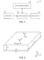
- FIG. 1 generally illustrates a block representation of an example data storage device 100.
- the data storage device 100 may take the form of a variety of different data storage technologies, such as rotating, solid state, and hybrid systems, which can be practiced in a variety of non-limiting mobile, server, and residential environments.
- the data storage device 100 may be configured at least with a controller 102 that directs inputted data signals 104 to a data storage element 106.
- the inputted data signals 104 may originate at an unlimited variety of locations, such as from external data storage devices and internal data cache, and correspond to data intended to be stored either temporarily or permanently on the data storage element 106.
- the size, speed, type, and number of data storage elements 106 are not limited to a particular configuration. That is, any storage element capable of retaining data for future access, such as a rotating data media, solid state cell, and hybrid data system, can be used to provide any data capacity and transfer speed configuration as the data storage element 106 either alone or in combination.
- the controller 102 may be capable of handling the inputted data 104 as well as providing data output signals 108 from the data storage element 106. As such, the controller 102 can selectively input data to and output data from one or more regions of the data storage element 106, either successively or concurrently.
- the data storage element 106 is constructed with at least one thin film magnetic layer that is magnetically fixed or free to allow data to be stored, written, and read via the controller 102.
- the thin film magnetic layer may be a part of a magnetoresistive lamination used to sense data programmed as data bits on a rotating data media.
- the thin film magnetic layer may be part of a solid state lamination, such as resistive random access memory (RRAM), that stores data with the formation of a filament between two electrodes.
- RRAM resistive random access memory
- FIG. 2 displays an isometric block representation of an example thin film magnetic layer 120 capable of being used in the data storage element 106 of FIG. 1 .
- the magnetic layer 120 is shown in a rectangular form with a thickness 122, stripe height 124, and width 126, but such shape and the particular dimensions of the layer 120 are not limited to a particular configuration.
- a uniaxial anisotropy 128 that is parallel to the transverse direction of the magnetic layer 120 and the X axis may be constructed to increase magnetic domain control versus omniaxial anisotropy.
- Such a uniaxial anisotropic orientation may allow for magnetically stable performance at predetermined magnetic flux densities, such as 2.4 Tesla.
- the uniaxial anisotropy 128 may alternatively be tuned to an angled orientation 130 with respect to both the X and Y axis to maintain magnetic performance of the layer 120 when the stripe height 124 is increased.
- an increasingly stripe height 126 can correspond with elevated magnetic instability that is mitigated by tilting the orientation of the uniaxial anisotropy 128 to the angled uniaxial anisotropy 130 oriented non-normal to the X and Y axis.
- a uniaxial anisotropy 132 oriented at an angle normal to the X axis may be formed in the magnetic layer 120 to bolster magnetic stability. For example, orienting the uniaxial anisotropy parallel to the width of the magnetic layer 120 along the X axis may lower erasure after write phenomenon as the anisotropy 128 allows magnetization to relax faster than if the anisotropy was oriented along the X axis, as in anisotropy 132, or angled to the X axis, as in anisotropy 130.
- the orientation of the uniaxial anisotropy of the magnetic layer 120 can be tuned along with the dimensions of the magnetic layer 120 to provide predetermined magnetic characteristics
- the application of heat to the magnetic layer can permanently alter the anisotropy and magnetic moment of a magnetic layer 120, regardless of how the anisotropy and magnetic moment was configured prior to the application of heat.
- tuning the temperature of the substrate on which the magnetic layer 120 is deposited and the angle in which the magnetic layer 120 is deposited can aid in maintaining anisotropy and moment characteristics subsequent to an application of heat.
- FIG. 3 shows an isometric block representation of the deposition of a magnetic layer 150 onto a substrate 152 in accordance with various embodiments.
- the magnetic layer 150 can be formed in any variety of shapes, dimensions, and materials, but in some embodiments is a rectangular thin film formed through the sputtered deposition of FeCo onto the substrate 152 at a predetermined oblique incidence angles ⁇ 1 , ⁇ 2 , ⁇ 3 that can range from 0 up to 90 degrees with respect to the Z axis.
- Static or dynamic oblique angle sputtering such as angles at or below 30 degrees, can produce elevated anisotropy, such as 200 Oe or above due to stress anisotropy being created by the agglomeration of vacancies and nano-voids formed behind growing crystallites due to shadowing effects of the oblique angle, without losing the inherent magnetic moment of the material. That is, growing crystallites block the line of sight from the incident beam of the sputtering gun 154 to produce vacancies in predictable locations that collectively produce stress anisotropy which leads to magnetic anisotropy in the film.
- the magnetic layer 160 of FIG. 4 generally illustrates how vacancies 162 align in predictable rows 164 aligned with a predetermined anisotropy direction 166 to produce uniaxial anisotropy along that direction 166.
- the thermal stability of the rows 164 becomes unstable in the presence of elevated heat as stress anisotropy lowers.
- conditions like annealing or heat treating the magnetic layer 160 can disturb the strength and direction of the uniaxial anisotropy.
- the material of the magnetic layer may be doped with a larger atomic radius element to mitigate thermal instability, but such efforts often lower the overall magnetic moment of the magnetic layer 160 to the detriment of high frequency data bit access operations.
- cooling the substrate such as substrate 152 of FIG. 3
- the magnetic layer 160 on which the magnetic layer 160 is deposited can reduce atomic mobility and more easily form vacancies 162 and nano-voids, which corresponds to increased thermal stability of the vacancy 162 alignment along the predetermined anisotropy direction 166.
- the anisotropy and magnetic moment are tuned by cryogenically cooling the substrate to a predetermined temperature, such as approximately 50 Kelvin, while the oblique angle of deposition is controlled.
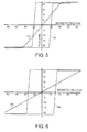
- FIGS. 5 and 6 respectively graph example operational data associated with magnetoresistive laminations including differently tuned magnetic layers in accordance with various embodiments.
- oblique deposition on a room temperature substrate is shown to provide easy 170 and hard 172 axis that is tuned to predetermined uniaxial anisotropy and magnetic moment characteristics.
- FIG. 5 can be altered by adjusting the oblique incidence angle of deposition, subsequent heat treatment or annealing may reduce or eliminate the tuned anisotropy and magnetic moment as vacancies in one or more magnetic layers move in crystal lattices due to thermal stresses induced by the application of heat.
- the easy 180 and hard 182 axis shown in FIG. 6 illustrate how tuning both oblique incidence angle and substrate temperature can produce increased uniaxial anisotropy, which is also more thermally stable due to reduce atomic mobility of the deposited magnetic material on a cryogenically cooled substrate.
- FIG. 7 provides an example thin film fabrication routine 200 performed in accordance with various embodiments.
- the routine 200 may begin by designing uniaxial anisotropy and magnetic moment that corresponds with magnetic performance optimized for application in step 202. That is, the anisotropy and magnetic moment can be designed in step 202 to provide magnetic characteristics, such as anisotropy direction and magnetic flux capacity, catered to the manner in which the thin film is to be used, such as a solid state lamination, magnetoresistive lamination, and proximity sensor.
- Step 204 first cools and maintains the substrate to a cryogenic temperature before step 206 configures a layer deposition means, such as a sputtering apparatus, to a predetermined oblique incidence angle.
- a layer deposition means such as a sputtering apparatus
- step 208 the deposition is evaluated in decision 210 as to whether adjustment of the substrate temperature or oblique incidence angle is to be adjusted. That is, whether the previously static substrate temperature and oblique incidence angle are to become dynamic while material is being deposited onto the substrate. If the determination from decision 210 is that modification is in order, step 212 alters the substrate temperature and/or the oblique incidence angle either individually or collectively while depositing material onto the cooled substrate.
- step 214 the deposition is terminated.
- Various embodiments maintain the substrate at a cryogenic temperature even after deposition while other embodiments submit the newly formed thin film to annealing heat treatments at elevated temperatures, both of which are not required or limiting to routine 200.
- routine 200 the thin film may be fabricated in isolation or as part of a lamination where additional layers are deposited atop the tuned thin film formed in routine 200.
- routine 200 is not limited to the process shown in FIG. 7 as various decisions and steps can be omitted, changed, and added. For example, multiple adjustments can be made to oblique incidence angle and/or substrate temperature between steps 208 and 214.
- the fabricated thin film is tuned with a uniaxial anisotropy direction, anisotropy strength, and magnetic moment that is optimized for stability, especially in regard to retaining magnetic characteristics after the application of heat.
- the configuration and material characteristics of the magnetic thin film described in the present disclosure allows for a magnetic layer optimized for anisotropic and thermal stability.
- the ability to tune the magnetic layer for increased uniaxial anisotropy with oblique incidence angle deposition combines with deposition onto a cryogenically cooled substrate to provide a robust magnetic thin film capable of increasing data bit capacity and data transfer rates of data storage devices.
- the claimed technology can readily be utilized in any number of magnetic applications, such as data sensing, data writing, and solid state data storage applications.
Landscapes
- Engineering & Computer Science (AREA)
- Manufacturing & Machinery (AREA)
- Nanotechnology (AREA)
- Chemical & Material Sciences (AREA)
- Power Engineering (AREA)
- Computer Hardware Design (AREA)
- Crystallography & Structural Chemistry (AREA)
- Physics & Mathematics (AREA)
- Thermal Sciences (AREA)
- Hall/Mr Elements (AREA)
- Thin Magnetic Films (AREA)
- Magnetic Heads (AREA)
- Mram Or Spin Memory Techniques (AREA)
Applications Claiming Priority (1)
| Application Number | Priority Date | Filing Date | Title |
|---|---|---|---|
| US13/689,409 US9034150B2 (en) | 2012-11-29 | 2012-11-29 | Thin film with tuned anisotropy and magnetic moment |
Publications (1)
| Publication Number | Publication Date |
|---|---|
| EP2738137A1 true EP2738137A1 (en) | 2014-06-04 |
Family
ID=49916807
Family Applications (1)
| Application Number | Title | Priority Date | Filing Date |
|---|---|---|---|
| EP20130194711 Ceased EP2738137A1 (en) | 2012-11-29 | 2013-11-27 | Thin film with tuned anisotropy and magnetic moment |
Country Status (5)
| Country | Link |
|---|---|
| US (1) | US9034150B2 (enExample) |
| EP (1) | EP2738137A1 (enExample) |
| JP (1) | JP6046597B2 (enExample) |
| KR (2) | KR20140070399A (enExample) |
| CN (1) | CN103855298B (enExample) |
Families Citing this family (3)
| Publication number | Priority date | Publication date | Assignee | Title |
|---|---|---|---|---|
| US9856557B1 (en) | 2016-01-22 | 2018-01-02 | Seagate Technology Llc | Fabrication of a multi-layered magnetic element |
| US10170691B2 (en) * | 2016-01-28 | 2019-01-01 | SK Hynix Inc. | Electronic device and method for fabricating the same |
| US11031032B1 (en) * | 2017-04-03 | 2021-06-08 | Seagate Technology Llc | Cryogenic magnetic alloys with less grain refinement dopants |
Citations (3)
| Publication number | Priority date | Publication date | Assignee | Title |
|---|---|---|---|---|
| US5764567A (en) * | 1996-11-27 | 1998-06-09 | International Business Machines Corporation | Magnetic tunnel junction device with nonferromagnetic interface layer for improved magnetic field response |
| US5948553A (en) * | 1996-04-25 | 1999-09-07 | Nec Corporation | Magnetic multilayer structure having magnetoresistance ratio and large magnetic sensitivity based on the giant magnetoresistance effect and process of fabrication thereof |
| US20020086182A1 (en) * | 2000-12-28 | 2002-07-04 | Nec Corporation | Spin tunnel magnetoresistive effect film and element, magnetoresistive sensor using same, magnetic apparatus, and method for manufacturing same |
Family Cites Families (19)
| Publication number | Priority date | Publication date | Assignee | Title |
|---|---|---|---|---|
| JPS62238614A (ja) * | 1986-04-09 | 1987-10-19 | Fujitsu Ltd | 異方性磁性膜の製造方法 |
| US5590389A (en) | 1994-12-23 | 1996-12-31 | Johnson Matthey Electronics, Inc. | Sputtering target with ultra-fine, oriented grains and method of making same |
| US6139951A (en) | 1997-12-12 | 2000-10-31 | Seagate Technology Llc | Magnetic recording medium with low temperature seedlayer for high signal-to-noise ratio |
| JP3677423B2 (ja) | 1999-12-28 | 2005-08-03 | 株式会社東芝 | 熱アシスト磁気記録方法及び熱アシスト磁気記録装置 |
| US6740397B1 (en) | 2000-05-24 | 2004-05-25 | Seagate Technology Llc | Subseedlayers for magnetic recording media |
| US6946039B1 (en) | 2000-11-02 | 2005-09-20 | Honeywell International Inc. | Physical vapor deposition targets, and methods of fabricating metallic materials |
| JP3619769B2 (ja) * | 2000-11-09 | 2005-02-16 | Tdk株式会社 | 磁気抵抗効果素子の製造方法 |
| JP2003198002A (ja) * | 2001-12-25 | 2003-07-11 | Fujitsu Ltd | 磁気抵抗効果膜および強磁性積層構造体 |
| US6791796B2 (en) | 2002-05-28 | 2004-09-14 | Seagate Technology Llc | Perpendicular writer with laminated main pole |
| JP2004326888A (ja) * | 2003-04-23 | 2004-11-18 | Sony Corp | 磁気記録媒体 |
| US6818961B1 (en) | 2003-06-30 | 2004-11-16 | Freescale Semiconductor, Inc. | Oblique deposition to induce magnetic anisotropy for MRAM cells |
| US7061731B2 (en) | 2003-11-17 | 2006-06-13 | Seagate Technology Llc | High magnetic anisotropy hard magnetic bias element |
| JP4529081B2 (ja) * | 2004-11-30 | 2010-08-25 | Tdk株式会社 | 磁性薄膜 |
| JP4503098B2 (ja) * | 2007-08-29 | 2010-07-14 | キヤノンアネルバ株式会社 | スパッタリングによる成膜方法とその装置 |
| US7914916B2 (en) | 2008-02-04 | 2011-03-29 | Seagate Technology Llc | Thermally stable high anisotropic high magnetic moment films |
| JPWO2009154009A1 (ja) * | 2008-06-20 | 2011-11-24 | キヤノンアネルバ株式会社 | 磁気抵抗素子の製造方法、スパッタ成膜チャンバー、スパッタ成膜チャンバーを有する磁気抵抗素子の製造装置、プログラム、記憶媒体 |
| US8776542B2 (en) * | 2009-12-25 | 2014-07-15 | Canon Anelva Corporation | Cooling system |
| JP2012140672A (ja) * | 2010-12-28 | 2012-07-26 | Canon Anelva Corp | スパッタリング装置 |
| JP5882934B2 (ja) * | 2012-05-09 | 2016-03-09 | シーゲイト テクノロジー エルエルシー | スパッタリング装置 |
-
2012
- 2012-11-29 US US13/689,409 patent/US9034150B2/en active Active
-
2013
- 2013-11-22 KR KR1020130143035A patent/KR20140070399A/ko not_active Ceased
- 2013-11-27 EP EP20130194711 patent/EP2738137A1/en not_active Ceased
- 2013-11-28 JP JP2013246158A patent/JP6046597B2/ja not_active Expired - Fee Related
- 2013-11-28 CN CN201310625298.0A patent/CN103855298B/zh not_active Expired - Fee Related
-
2015
- 2015-02-27 KR KR20150028228A patent/KR20150035892A/ko not_active Withdrawn
Patent Citations (3)
| Publication number | Priority date | Publication date | Assignee | Title |
|---|---|---|---|---|
| US5948553A (en) * | 1996-04-25 | 1999-09-07 | Nec Corporation | Magnetic multilayer structure having magnetoresistance ratio and large magnetic sensitivity based on the giant magnetoresistance effect and process of fabrication thereof |
| US5764567A (en) * | 1996-11-27 | 1998-06-09 | International Business Machines Corporation | Magnetic tunnel junction device with nonferromagnetic interface layer for improved magnetic field response |
| US20020086182A1 (en) * | 2000-12-28 | 2002-07-04 | Nec Corporation | Spin tunnel magnetoresistive effect film and element, magnetoresistive sensor using same, magnetic apparatus, and method for manufacturing same |
Non-Patent Citations (1)
| Title |
|---|
| HAWKEYE MATTHEW ET AL: "Glancing angle deposition: Fabrication, properties, and applications of micro- and nanostructured thin films", JOURNAL OF VACUUM SCIENCE AND TECHNOLOGY: PART A, AVS /AIP, MELVILLE, NY., US, vol. 25, no. 5, 30 July 2007 (2007-07-30), pages 1317 - 1335, XP012102748, ISSN: 0734-2101, DOI: 10.1116/1.2764082 * |
Also Published As
| Publication number | Publication date |
|---|---|
| KR20140070399A (ko) | 2014-06-10 |
| CN103855298B (zh) | 2017-12-22 |
| JP2014112677A (ja) | 2014-06-19 |
| US9034150B2 (en) | 2015-05-19 |
| KR20150035892A (ko) | 2015-04-07 |
| JP6046597B2 (ja) | 2016-12-21 |
| CN103855298A (zh) | 2014-06-11 |
| US20140147702A1 (en) | 2014-05-29 |
Similar Documents
| Publication | Publication Date | Title |
|---|---|---|
| Kim et al. | Field‐free switching of magnetization by tilting the perpendicular magnetic anisotropy of Gd/Co multilayers | |
| US8133332B2 (en) | Method for preparing FePt media at low ordering temperature and fabrication of exchange coupled composite media and gradient anisotropy media for magnetic recording | |
| US20140268417A1 (en) | Bottom shield stabilized magnetic seed layer | |
| US9034150B2 (en) | Thin film with tuned anisotropy and magnetic moment | |
| US9142226B2 (en) | Thin film with tuned grain size | |
| KR101336861B1 (ko) | 삼중층 자기 센서들의 튜닝된 각진 단축 이방성 | |
| Zhao et al. | Magnetic properties and anomalous Hall effect of Mn3Sn thin films controlled by defects and ferroelectric 0.7 Pb (Mg1/3Nb2/3) O3–0.3 PbTiO3 substrate | |
| US20130288078A1 (en) | Thin Film with Reduced Stress Anisotropy | |
| CN108695431B (zh) | 一种磁性隧道结的平坦化方法 | |
| US9240200B2 (en) | Magnetic element with crossed anisotropies | |
| Xiao et al. | Temperature dependence of interlayer coupling between perpendicular magnetic [CoFeB/Pd] multilayers: Influence of interfacial CoFeB layer | |
| WO2016054489A1 (en) | L1o-ORDERED MnAI THIN FILMS WITH HIGH PERPENDICULAR MAGNETIC ANISOTROPY, AND STRUCTURES AND DEVICES MADE THEREWITH | |
| Adam et al. | Ferromagnetism modulation by phase change in Mn-doped GeTe chalcogenide magnetic materials | |
| US20180108833A1 (en) | Method and system for providing magnetic junctions usable in spin transfer torque applications utilizing interstitial glass-forming agent(s) | |
| Yu et al. | Enhancement of perpendicular coercivity for CoPt top layer in CoPt/AlN multilayer structure | |
| US9349391B2 (en) | Controlling magnetic layer anisotropy field by oblique angle static deposition | |
| US7161763B2 (en) | GMR sensor with oriented hard bias stabilization | |
| US20160035376A1 (en) | Data Reader with Tuned Microstructure | |
| Chi et al. | Improvement and stabilization of exchange bias in ferromagnet/antiferromagnet/ferromagnet trilayers | |
| Shoup et al. | Oscillation of interlayer coupling in epitaxial FePd| Ir| FePd (001) perpendicular synthetic antiferromagnet | |
| Fernandez-Outon et al. | Interfacial spin effects on Hex in metallic polycrystalline exchange biased systems | |
| George et al. | Nanostructure and magnetic properties of L1 FePt: X films | |
| Balymov et al. | Effect of Selective Thermomagnetic Treatment on Unidirectional Magnetic Anisotropy in FeNi/TbCo Films | |
| CN103531209B (zh) | 具有已调晶粒尺寸的薄膜 | |
| KR101078872B1 (ko) | 자성 박막 부재 및 그 제조 방법 |
Legal Events
| Date | Code | Title | Description |
|---|---|---|---|
| PUAI | Public reference made under article 153(3) epc to a published international application that has entered the european phase |
Free format text: ORIGINAL CODE: 0009012 |
|
| 17P | Request for examination filed |
Effective date: 20131216 |
|
| AK | Designated contracting states |
Kind code of ref document: A1 Designated state(s): AL AT BE BG CH CY CZ DE DK EE ES FI FR GB GR HR HU IE IS IT LI LT LU LV MC MK MT NL NO PL PT RO RS SE SI SK SM TR |
|
| AX | Request for extension of the european patent |
Extension state: BA ME |
|
| RBV | Designated contracting states (corrected) |
Designated state(s): AL AT BE BG CH CY CZ DE DK EE ES FI FR GB GR HR HU IE IS IT LI LT LU LV MC MK MT NL NO PL PT RO RS SE SI SK SM TR |
|
| 17Q | First examination report despatched |
Effective date: 20150611 |
|
| STAA | Information on the status of an ep patent application or granted ep patent |
Free format text: STATUS: THE APPLICATION HAS BEEN REFUSED |
|
| 18R | Application refused |
Effective date: 20161202 |