EP2734601B1 - Oxyde de nickel électrochromique dopé simultanément avec du lithium et un dopant métallique - Google Patents
Oxyde de nickel électrochromique dopé simultanément avec du lithium et un dopant métallique Download PDFInfo
- Publication number
- EP2734601B1 EP2734601B1 EP12744150.9A EP12744150A EP2734601B1 EP 2734601 B1 EP2734601 B1 EP 2734601B1 EP 12744150 A EP12744150 A EP 12744150A EP 2734601 B1 EP2734601 B1 EP 2734601B1
- Authority
- EP
- European Patent Office
- Prior art keywords
- layer
- electrochromic
- counter electrode
- oxide
- lithium
- Prior art date
- Legal status (The legal status is an assumption and is not a legal conclusion. Google has not performed a legal analysis and makes no representation as to the accuracy of the status listed.)
- Active
Links
- 229910052744 lithium Inorganic materials 0.000 title claims description 43
- WHXSMMKQMYFTQS-UHFFFAOYSA-N Lithium Chemical compound [Li] WHXSMMKQMYFTQS-UHFFFAOYSA-N 0.000 title claims description 35
- 229910052751 metal Inorganic materials 0.000 title claims description 31
- 239000002184 metal Substances 0.000 title claims description 31
- GNRSAWUEBMWBQH-UHFFFAOYSA-N oxonickel Chemical compound [Ni]=O GNRSAWUEBMWBQH-UHFFFAOYSA-N 0.000 title description 33
- 229910000480 nickel oxide Inorganic materials 0.000 title description 30
- 239000002019 doping agent Substances 0.000 title 1
- 239000010416 ion conductor Substances 0.000 claims description 34
- 238000000034 method Methods 0.000 claims description 30
- 230000003647 oxidation Effects 0.000 claims description 26
- 238000007254 oxidation reaction Methods 0.000 claims description 26
- 150000002500 ions Chemical class 0.000 claims description 24
- 238000000151 deposition Methods 0.000 claims description 22
- 229910015947 LixNi Inorganic materials 0.000 claims description 13
- 229910044991 metal oxide Inorganic materials 0.000 claims description 12
- 238000005546 reactive sputtering Methods 0.000 claims description 12
- 150000004706 metal oxides Chemical class 0.000 claims description 9
- 238000002360 preparation method Methods 0.000 claims description 5
- 229910052720 vanadium Inorganic materials 0.000 claims description 5
- PWHULOQIROXLJO-UHFFFAOYSA-N Manganese Chemical compound [Mn] PWHULOQIROXLJO-UHFFFAOYSA-N 0.000 claims description 4
- JOPOVCBBYLSVDA-UHFFFAOYSA-N chromium(6+) Chemical compound [Cr+6] JOPOVCBBYLSVDA-UHFFFAOYSA-N 0.000 claims description 4
- XHGGEBRKUWZHEK-UHFFFAOYSA-L tellurate Chemical compound [O-][Te]([O-])(=O)=O XHGGEBRKUWZHEK-UHFFFAOYSA-L 0.000 claims description 4
- 229910052710 silicon Inorganic materials 0.000 claims description 3
- 239000010410 layer Substances 0.000 description 169
- 239000000463 material Substances 0.000 description 111
- PXHVJJICTQNCMI-UHFFFAOYSA-N nickel Substances [Ni] PXHVJJICTQNCMI-UHFFFAOYSA-N 0.000 description 87
- 230000003287 optical effect Effects 0.000 description 54
- 239000010408 film Substances 0.000 description 47
- 230000005540 biological transmission Effects 0.000 description 24
- 239000002159 nanocrystal Substances 0.000 description 20
- 239000000758 substrate Substances 0.000 description 20
- 229910001416 lithium ion Inorganic materials 0.000 description 16
- 238000002056 X-ray absorption spectroscopy Methods 0.000 description 15
- 238000001228 spectrum Methods 0.000 description 14
- 239000000203 mixture Substances 0.000 description 13
- 229910052760 oxygen Inorganic materials 0.000 description 13
- 238000004544 sputter deposition Methods 0.000 description 13
- 230000008859 change Effects 0.000 description 12
- 238000000576 coating method Methods 0.000 description 11
- 229910052759 nickel Inorganic materials 0.000 description 11
- 239000001301 oxygen Substances 0.000 description 11
- QVGXLLKOCUKJST-UHFFFAOYSA-N atomic oxygen Chemical compound [O] QVGXLLKOCUKJST-UHFFFAOYSA-N 0.000 description 10
- -1 hydrogen ions Chemical class 0.000 description 10
- 239000010409 thin film Substances 0.000 description 10
- 229910001930 tungsten oxide Inorganic materials 0.000 description 10
- 125000004429 atom Chemical group 0.000 description 9
- QGLKJKCYBOYXKC-UHFFFAOYSA-N nonaoxidotritungsten Chemical compound O=[W]1(=O)O[W](=O)(=O)O[W](=O)(=O)O1 QGLKJKCYBOYXKC-UHFFFAOYSA-N 0.000 description 9
- 238000002834 transmittance Methods 0.000 description 9
- 239000004020 conductor Substances 0.000 description 8
- 238000002484 cyclic voltammetry Methods 0.000 description 8
- 230000008021 deposition Effects 0.000 description 8
- 239000003792 electrolyte Substances 0.000 description 8
- 230000000670 limiting effect Effects 0.000 description 8
- HBBGRARXTFLTSG-UHFFFAOYSA-N Lithium ion Chemical compound [Li+] HBBGRARXTFLTSG-UHFFFAOYSA-N 0.000 description 7
- 238000000026 X-ray photoelectron spectrum Methods 0.000 description 7
- 239000013078 crystal Substances 0.000 description 7
- 230000015572 biosynthetic process Effects 0.000 description 6
- 239000011521 glass Substances 0.000 description 6
- 238000011065 in-situ storage Methods 0.000 description 6
- 238000009830 intercalation Methods 0.000 description 6
- 230000002687 intercalation Effects 0.000 description 6
- 239000011159 matrix material Substances 0.000 description 6
- 230000007704 transition Effects 0.000 description 6
- 229910001323 Li2O2 Inorganic materials 0.000 description 5
- 229910005855 NiOx Inorganic materials 0.000 description 5
- 238000010521 absorption reaction Methods 0.000 description 5
- 239000000919 ceramic Substances 0.000 description 5
- 239000011248 coating agent Substances 0.000 description 5
- 230000007246 mechanism Effects 0.000 description 5
- 238000005240 physical vapour deposition Methods 0.000 description 5
- 239000004033 plastic Substances 0.000 description 5
- 229920003023 plastic Polymers 0.000 description 5
- 230000002829 reductive effect Effects 0.000 description 5
- 230000002441 reversible effect Effects 0.000 description 5
- 239000010936 titanium Substances 0.000 description 5
- 229910052726 zirconium Inorganic materials 0.000 description 5
- XKRFYHLGVUSROY-UHFFFAOYSA-N Argon Chemical compound [Ar] XKRFYHLGVUSROY-UHFFFAOYSA-N 0.000 description 4
- FUJCRWPEOMXPAD-UHFFFAOYSA-N Li2O Inorganic materials [Li+].[Li+].[O-2] FUJCRWPEOMXPAD-UHFFFAOYSA-N 0.000 description 4
- VYPSYNLAJGMNEJ-UHFFFAOYSA-N Silicium dioxide Chemical compound O=[Si]=O VYPSYNLAJGMNEJ-UHFFFAOYSA-N 0.000 description 4
- 238000002441 X-ray diffraction Methods 0.000 description 4
- XLOMVQKBTHCTTD-UHFFFAOYSA-N Zinc monoxide Chemical compound [Zn]=O XLOMVQKBTHCTTD-UHFFFAOYSA-N 0.000 description 4
- MCMNRKCIXSYSNV-UHFFFAOYSA-N Zirconium dioxide Chemical compound O=[Zr]=O MCMNRKCIXSYSNV-UHFFFAOYSA-N 0.000 description 4
- XHCLAFWTIXFWPH-UHFFFAOYSA-N [O-2].[O-2].[O-2].[O-2].[O-2].[V+5].[V+5] Chemical group [O-2].[O-2].[O-2].[O-2].[O-2].[V+5].[V+5] XHCLAFWTIXFWPH-UHFFFAOYSA-N 0.000 description 4
- 238000000862 absorption spectrum Methods 0.000 description 4
- 239000000654 additive Substances 0.000 description 4
- 238000004061 bleaching Methods 0.000 description 4
- XUCJHNOBJLKZNU-UHFFFAOYSA-M dilithium;hydroxide Chemical compound [Li+].[Li+].[OH-] XUCJHNOBJLKZNU-UHFFFAOYSA-M 0.000 description 4
- 230000000694 effects Effects 0.000 description 4
- 238000001704 evaporation Methods 0.000 description 4
- 230000008020 evaporation Effects 0.000 description 4
- 239000007789 gas Substances 0.000 description 4
- 238000004519 manufacturing process Methods 0.000 description 4
- 230000008569 process Effects 0.000 description 4
- 230000004044 response Effects 0.000 description 4
- 238000003860 storage Methods 0.000 description 4
- 239000000126 substance Substances 0.000 description 4
- 229910001887 tin oxide Inorganic materials 0.000 description 4
- 229910001935 vanadium oxide Inorganic materials 0.000 description 4
- CBENFWSGALASAD-UHFFFAOYSA-N Ozone Chemical compound [O-][O+]=O CBENFWSGALASAD-UHFFFAOYSA-N 0.000 description 3
- 230000009102 absorption Effects 0.000 description 3
- 238000005229 chemical vapour deposition Methods 0.000 description 3
- 230000000295 complement effect Effects 0.000 description 3
- 239000002131 composite material Substances 0.000 description 3
- 230000001351 cycling effect Effects 0.000 description 3
- 239000011262 electrochemically active material Substances 0.000 description 3
- 238000009396 hybridization Methods 0.000 description 3
- AMGQUBHHOARCQH-UHFFFAOYSA-N indium;oxotin Chemical compound [In].[Sn]=O AMGQUBHHOARCQH-UHFFFAOYSA-N 0.000 description 3
- 238000001095 inductively coupled plasma mass spectrometry Methods 0.000 description 3
- 238000003780 insertion Methods 0.000 description 3
- 230000037431 insertion Effects 0.000 description 3
- 230000031700 light absorption Effects 0.000 description 3
- HPGPEWYJWRWDTP-UHFFFAOYSA-N lithium peroxide Chemical compound [Li+].[Li+].[O-][O-] HPGPEWYJWRWDTP-UHFFFAOYSA-N 0.000 description 3
- 238000001755 magnetron sputter deposition Methods 0.000 description 3
- 229910001092 metal group alloy Inorganic materials 0.000 description 3
- RUOJZAUFBMNUDX-UHFFFAOYSA-N propylene carbonate Chemical compound CC1COC(=O)O1 RUOJZAUFBMNUDX-UHFFFAOYSA-N 0.000 description 3
- 230000009467 reduction Effects 0.000 description 3
- 239000007787 solid Substances 0.000 description 3
- 241000894007 species Species 0.000 description 3
- XOLBLPGZBRYERU-UHFFFAOYSA-N tin dioxide Chemical compound O=[Sn]=O XOLBLPGZBRYERU-UHFFFAOYSA-N 0.000 description 3
- 229910052723 transition metal Inorganic materials 0.000 description 3
- 150000003624 transition metals Chemical class 0.000 description 3
- 238000004627 transmission electron microscopy Methods 0.000 description 3
- XLYOFNOQVPJJNP-UHFFFAOYSA-N water Substances O XLYOFNOQVPJJNP-UHFFFAOYSA-N 0.000 description 3
- CSCPPACGZOOCGX-UHFFFAOYSA-N Acetone Chemical compound CC(C)=O CSCPPACGZOOCGX-UHFFFAOYSA-N 0.000 description 2
- 229920002574 CR-39 Polymers 0.000 description 2
- QPLDLSVMHZLSFG-UHFFFAOYSA-N Copper oxide Chemical compound [Cu]=O QPLDLSVMHZLSFG-UHFFFAOYSA-N 0.000 description 2
- KFZMGEQAYNKOFK-UHFFFAOYSA-N Isopropanol Chemical compound CC(C)O KFZMGEQAYNKOFK-UHFFFAOYSA-N 0.000 description 2
- 229910013292 LiNiO Inorganic materials 0.000 description 2
- ZOKXTWBITQBERF-UHFFFAOYSA-N Molybdenum Chemical compound [Mo] ZOKXTWBITQBERF-UHFFFAOYSA-N 0.000 description 2
- GWEVSGVZZGPLCZ-UHFFFAOYSA-N Titan oxide Chemical compound O=[Ti]=O GWEVSGVZZGPLCZ-UHFFFAOYSA-N 0.000 description 2
- 238000004833 X-ray photoelectron spectroscopy Methods 0.000 description 2
- 238000005299 abrasion Methods 0.000 description 2
- 239000012736 aqueous medium Substances 0.000 description 2
- 229910052786 argon Inorganic materials 0.000 description 2
- 239000012300 argon atmosphere Substances 0.000 description 2
- 230000008901 benefit Effects 0.000 description 2
- 239000007844 bleaching agent Substances 0.000 description 2
- 238000004364 calculation method Methods 0.000 description 2
- 238000012512 characterization method Methods 0.000 description 2
- 238000004040 coloring Methods 0.000 description 2
- 238000000354 decomposition reaction Methods 0.000 description 2
- 230000007423 decrease Effects 0.000 description 2
- 230000003247 decreasing effect Effects 0.000 description 2
- 238000005137 deposition process Methods 0.000 description 2
- QDOXWKRWXJOMAK-UHFFFAOYSA-N dichromium trioxide Chemical compound O=[Cr]O[Cr]=O QDOXWKRWXJOMAK-UHFFFAOYSA-N 0.000 description 2
- 238000009792 diffusion process Methods 0.000 description 2
- GNTDGMZSJNCJKK-UHFFFAOYSA-N divanadium pentaoxide Chemical compound O=[V](=O)O[V](=O)=O GNTDGMZSJNCJKK-UHFFFAOYSA-N 0.000 description 2
- 239000007772 electrode material Substances 0.000 description 2
- 238000000445 field-emission scanning electron microscopy Methods 0.000 description 2
- 238000002173 high-resolution transmission electron microscopy Methods 0.000 description 2
- 229910003437 indium oxide Inorganic materials 0.000 description 2
- PJXISJQVUVHSOJ-UHFFFAOYSA-N indium(iii) oxide Chemical compound [O-2].[O-2].[O-2].[In+3].[In+3] PJXISJQVUVHSOJ-UHFFFAOYSA-N 0.000 description 2
- 238000000608 laser ablation Methods 0.000 description 2
- MHCFAGZWMAWTNR-UHFFFAOYSA-M lithium perchlorate Chemical compound [Li+].[O-]Cl(=O)(=O)=O MHCFAGZWMAWTNR-UHFFFAOYSA-M 0.000 description 2
- 230000007774 longterm Effects 0.000 description 2
- 238000005259 measurement Methods 0.000 description 2
- 150000002739 metals Chemical class 0.000 description 2
- 229910052750 molybdenum Inorganic materials 0.000 description 2
- 239000011733 molybdenum Substances 0.000 description 2
- JKQOBWVOAYFWKG-UHFFFAOYSA-N molybdenum trioxide Chemical compound O=[Mo](=O)=O JKQOBWVOAYFWKG-UHFFFAOYSA-N 0.000 description 2
- 239000002114 nanocomposite Substances 0.000 description 2
- 230000007935 neutral effect Effects 0.000 description 2
- ZKATWMILCYLAPD-UHFFFAOYSA-N niobium pentoxide Chemical compound O=[Nb](=O)O[Nb](=O)=O ZKATWMILCYLAPD-UHFFFAOYSA-N 0.000 description 2
- UPWOEMHINGJHOB-UHFFFAOYSA-N oxo(oxocobaltiooxy)cobalt Chemical compound O=[Co]O[Co]=O UPWOEMHINGJHOB-UHFFFAOYSA-N 0.000 description 2
- 125000004430 oxygen atom Chemical group O* 0.000 description 2
- 230000005855 radiation Effects 0.000 description 2
- 238000001552 radio frequency sputter deposition Methods 0.000 description 2
- 238000009877 rendering Methods 0.000 description 2
- 229910001925 ruthenium oxide Inorganic materials 0.000 description 2
- WOCIAKWEIIZHES-UHFFFAOYSA-N ruthenium(iv) oxide Chemical compound O=[Ru]=O WOCIAKWEIIZHES-UHFFFAOYSA-N 0.000 description 2
- 238000001878 scanning electron micrograph Methods 0.000 description 2
- 239000000377 silicon dioxide Substances 0.000 description 2
- 238000003980 solgel method Methods 0.000 description 2
- 239000002344 surface layer Substances 0.000 description 2
- 238000003786 synthesis reaction Methods 0.000 description 2
- 239000013077 target material Substances 0.000 description 2
- 229910052721 tungsten Inorganic materials 0.000 description 2
- 238000001392 ultraviolet--visible--near infrared spectroscopy Methods 0.000 description 2
- 239000011787 zinc oxide Substances 0.000 description 2
- NNWNNQTUZYVQRK-UHFFFAOYSA-N 5-bromo-1h-pyrrolo[2,3-c]pyridine-2-carboxylic acid Chemical compound BrC1=NC=C2NC(C(=O)O)=CC2=C1 NNWNNQTUZYVQRK-UHFFFAOYSA-N 0.000 description 1
- IJGRMHOSHXDMSA-UHFFFAOYSA-N Atomic nitrogen Chemical compound N#N IJGRMHOSHXDMSA-UHFFFAOYSA-N 0.000 description 1
- 101100317222 Borrelia hermsii vsp3 gene Proteins 0.000 description 1
- DGAQECJNVWCQMB-PUAWFVPOSA-M Ilexoside XXIX Chemical compound C[C@@H]1CC[C@@]2(CC[C@@]3(C(=CC[C@H]4[C@]3(CC[C@@H]5[C@@]4(CC[C@@H](C5(C)C)OS(=O)(=O)[O-])C)C)[C@@H]2[C@]1(C)O)C)C(=O)O[C@H]6[C@@H]([C@H]([C@@H]([C@H](O6)CO)O)O)O.[Na+] DGAQECJNVWCQMB-PUAWFVPOSA-M 0.000 description 1
- 229910014151 LixNiOy Inorganic materials 0.000 description 1
- 229910000990 Ni alloy Inorganic materials 0.000 description 1
- BPQQTUXANYXVAA-UHFFFAOYSA-N Orthosilicate Chemical compound [O-][Si]([O-])([O-])[O-] BPQQTUXANYXVAA-UHFFFAOYSA-N 0.000 description 1
- 239000004952 Polyamide Substances 0.000 description 1
- 239000004793 Polystyrene Substances 0.000 description 1
- ZLMJMSJWJFRBEC-UHFFFAOYSA-N Potassium Chemical compound [K] ZLMJMSJWJFRBEC-UHFFFAOYSA-N 0.000 description 1
- BQCADISMDOOEFD-UHFFFAOYSA-N Silver Chemical compound [Ag] BQCADISMDOOEFD-UHFFFAOYSA-N 0.000 description 1
- 229910052771 Terbium Inorganic materials 0.000 description 1
- RTAQQCXQSZGOHL-UHFFFAOYSA-N Titanium Chemical compound [Ti] RTAQQCXQSZGOHL-UHFFFAOYSA-N 0.000 description 1
- 238000002083 X-ray spectrum Methods 0.000 description 1
- QCWXUUIWCKQGHC-UHFFFAOYSA-N Zirconium Chemical compound [Zr] QCWXUUIWCKQGHC-UHFFFAOYSA-N 0.000 description 1
- 0 [*+]CCCC#CCC#N Chemical compound [*+]CCCC#CCC#N 0.000 description 1
- YJZATOSJMRIRIW-UHFFFAOYSA-N [Ir]=O Chemical class [Ir]=O YJZATOSJMRIRIW-UHFFFAOYSA-N 0.000 description 1
- JFBZPFYRPYOZCQ-UHFFFAOYSA-N [Li].[Al] Chemical compound [Li].[Al] JFBZPFYRPYOZCQ-UHFFFAOYSA-N 0.000 description 1
- YJSAVIWBELEHDD-UHFFFAOYSA-N [Li].[Si]=O Chemical compound [Li].[Si]=O YJSAVIWBELEHDD-UHFFFAOYSA-N 0.000 description 1
- LFZYLAXEYRJERI-UHFFFAOYSA-N [Li].[Zr] Chemical compound [Li].[Zr] LFZYLAXEYRJERI-UHFFFAOYSA-N 0.000 description 1
- NIXOWILDQLNWCW-UHFFFAOYSA-N acrylic acid group Chemical group C(C=C)(=O)O NIXOWILDQLNWCW-UHFFFAOYSA-N 0.000 description 1
- 229910045601 alloy Inorganic materials 0.000 description 1
- 239000000956 alloy Substances 0.000 description 1
- 229910052782 aluminium Inorganic materials 0.000 description 1
- XAGFODPZIPBFFR-UHFFFAOYSA-N aluminium Chemical compound [Al] XAGFODPZIPBFFR-UHFFFAOYSA-N 0.000 description 1
- PGTAKMRAYVRICI-UHFFFAOYSA-N aluminum lithium borate Chemical compound B([O-])([O-])[O-].[Al+3].[Li+] PGTAKMRAYVRICI-UHFFFAOYSA-N 0.000 description 1
- 238000004458 analytical method Methods 0.000 description 1
- 230000003667 anti-reflective effect Effects 0.000 description 1
- 238000013459 approach Methods 0.000 description 1
- 230000004888 barrier function Effects 0.000 description 1
- 230000000903 blocking effect Effects 0.000 description 1
- 239000003990 capacitor Substances 0.000 description 1
- 229910052799 carbon Inorganic materials 0.000 description 1
- 229910010293 ceramic material Inorganic materials 0.000 description 1
- 238000006243 chemical reaction Methods 0.000 description 1
- 239000007795 chemical reaction product Substances 0.000 description 1
- 239000013065 commercial product Substances 0.000 description 1
- 150000001875 compounds Chemical class 0.000 description 1
- 238000005090 crystal field Methods 0.000 description 1
- 230000007812 deficiency Effects 0.000 description 1
- 239000008367 deionised water Substances 0.000 description 1
- 229910021641 deionized water Inorganic materials 0.000 description 1
- 229910001873 dinitrogen Inorganic materials 0.000 description 1
- 239000006185 dispersion Substances 0.000 description 1
- 230000005684 electric field Effects 0.000 description 1
- 238000002848 electrochemical method Methods 0.000 description 1
- 238000002149 energy-dispersive X-ray emission spectroscopy Methods 0.000 description 1
- 238000002474 experimental method Methods 0.000 description 1
- 230000002349 favourable effect Effects 0.000 description 1
- 230000005669 field effect Effects 0.000 description 1
- 239000005357 flat glass Substances 0.000 description 1
- 239000005329 float glass Substances 0.000 description 1
- 230000004313 glare Effects 0.000 description 1
- PCHJSUWPFVWCPO-UHFFFAOYSA-N gold Chemical compound [Au] PCHJSUWPFVWCPO-UHFFFAOYSA-N 0.000 description 1
- 229910052737 gold Inorganic materials 0.000 description 1
- 239000010931 gold Substances 0.000 description 1
- JEGUKCSWCFPDGT-UHFFFAOYSA-N h2o hydrate Chemical compound O.O JEGUKCSWCFPDGT-UHFFFAOYSA-N 0.000 description 1
- 229910052735 hafnium Inorganic materials 0.000 description 1
- VBJZVLUMGGDVMO-UHFFFAOYSA-N hafnium atom Chemical compound [Hf] VBJZVLUMGGDVMO-UHFFFAOYSA-N 0.000 description 1
- 238000010438 heat treatment Methods 0.000 description 1
- 239000001257 hydrogen Substances 0.000 description 1
- 229910052739 hydrogen Inorganic materials 0.000 description 1
- 230000006872 improvement Effects 0.000 description 1
- 239000012535 impurity Substances 0.000 description 1
- 230000003993 interaction Effects 0.000 description 1
- 229910000765 intermetallic Inorganic materials 0.000 description 1
- 229910052741 iridium Inorganic materials 0.000 description 1
- GKOZUEZYRPOHIO-UHFFFAOYSA-N iridium atom Chemical compound [Ir] GKOZUEZYRPOHIO-UHFFFAOYSA-N 0.000 description 1
- 229910000457 iridium oxide Inorganic materials 0.000 description 1
- 229910052747 lanthanoid Inorganic materials 0.000 description 1
- 239000004973 liquid crystal related substance Substances 0.000 description 1
- 239000011244 liquid electrolyte Substances 0.000 description 1
- 238000006138 lithiation reaction Methods 0.000 description 1
- 229910021450 lithium metal oxide Inorganic materials 0.000 description 1
- PAZHGORSDKKUPI-UHFFFAOYSA-N lithium metasilicate Chemical compound [Li+].[Li+].[O-][Si]([O-])=O PAZHGORSDKKUPI-UHFFFAOYSA-N 0.000 description 1
- GQYHUHYESMUTHG-UHFFFAOYSA-N lithium niobate Chemical compound [Li+].[O-][Nb](=O)=O GQYHUHYESMUTHG-UHFFFAOYSA-N 0.000 description 1
- IDBFBDSKYCUNPW-UHFFFAOYSA-N lithium nitride Chemical compound [Li]N([Li])[Li] IDBFBDSKYCUNPW-UHFFFAOYSA-N 0.000 description 1
- 229910001486 lithium perchlorate Inorganic materials 0.000 description 1
- 229910052912 lithium silicate Inorganic materials 0.000 description 1
- BAEKJBILAYEFEI-UHFFFAOYSA-N lithium;oxotungsten Chemical compound [Li].[W]=O BAEKJBILAYEFEI-UHFFFAOYSA-N 0.000 description 1
- GEYXPJBPASPPLI-UHFFFAOYSA-N manganese(III) oxide Inorganic materials O=[Mn]O[Mn]=O GEYXPJBPASPPLI-UHFFFAOYSA-N 0.000 description 1
- 238000000691 measurement method Methods 0.000 description 1
- 239000002609 medium Substances 0.000 description 1
- 238000001000 micrograph Methods 0.000 description 1
- 238000012986 modification Methods 0.000 description 1
- 230000004048 modification Effects 0.000 description 1
- 229910000476 molybdenum oxide Inorganic materials 0.000 description 1
- 239000002105 nanoparticle Substances 0.000 description 1
- 238000006386 neutralization reaction Methods 0.000 description 1
- GNMQOUGYKPVJRR-UHFFFAOYSA-N nickel(III) oxide Inorganic materials [O-2].[O-2].[O-2].[Ni+3].[Ni+3] GNMQOUGYKPVJRR-UHFFFAOYSA-N 0.000 description 1
- BFDHFSHZJLFAMC-UHFFFAOYSA-L nickel(ii) hydroxide Chemical class [OH-].[OH-].[Ni+2] BFDHFSHZJLFAMC-UHFFFAOYSA-L 0.000 description 1
- 150000004767 nitrides Chemical class 0.000 description 1
- 230000001590 oxidative effect Effects 0.000 description 1
- PZFKDUMHDHEBLD-UHFFFAOYSA-N oxo(oxonickeliooxy)nickel Chemical compound O=[Ni]O[Ni]=O PZFKDUMHDHEBLD-UHFFFAOYSA-N 0.000 description 1
- PQQKPALAQIIWST-UHFFFAOYSA-N oxomolybdenum Chemical class [Mo]=O PQQKPALAQIIWST-UHFFFAOYSA-N 0.000 description 1
- VVRQVWSVLMGPRN-UHFFFAOYSA-N oxotungsten Chemical class [W]=O VVRQVWSVLMGPRN-UHFFFAOYSA-N 0.000 description 1
- BPUBBGLMJRNUCC-UHFFFAOYSA-N oxygen(2-);tantalum(5+) Chemical compound [O-2].[O-2].[O-2].[O-2].[O-2].[Ta+5].[Ta+5] BPUBBGLMJRNUCC-UHFFFAOYSA-N 0.000 description 1
- SOQBVABWOPYFQZ-UHFFFAOYSA-N oxygen(2-);titanium(4+) Chemical class [O-2].[O-2].[Ti+4] SOQBVABWOPYFQZ-UHFFFAOYSA-N 0.000 description 1
- 230000036961 partial effect Effects 0.000 description 1
- 230000035515 penetration Effects 0.000 description 1
- 238000005191 phase separation Methods 0.000 description 1
- 229920002285 poly(styrene-co-acrylonitrile) Polymers 0.000 description 1
- 229920002647 polyamide Polymers 0.000 description 1
- 229920000515 polycarbonate Polymers 0.000 description 1
- 239000004417 polycarbonate Substances 0.000 description 1
- 229920000728 polyester Polymers 0.000 description 1
- 229920000306 polymethylpentene Polymers 0.000 description 1
- 239000011116 polymethylpentene Substances 0.000 description 1
- 229920001296 polysiloxane Polymers 0.000 description 1
- 229920002223 polystyrene Polymers 0.000 description 1
- 229910052700 potassium Inorganic materials 0.000 description 1
- 239000011591 potassium Substances 0.000 description 1
- 230000002035 prolonged effect Effects 0.000 description 1
- 230000001681 protective effect Effects 0.000 description 1
- 150000003839 salts Chemical class 0.000 description 1
- 238000007086 side reaction Methods 0.000 description 1
- 235000012239 silicon dioxide Nutrition 0.000 description 1
- LIVNPJMFVYWSIS-UHFFFAOYSA-N silicon monoxide Chemical class [Si-]#[O+] LIVNPJMFVYWSIS-UHFFFAOYSA-N 0.000 description 1
- 229910052814 silicon oxide Inorganic materials 0.000 description 1
- 229910052709 silver Inorganic materials 0.000 description 1
- 239000004332 silver Substances 0.000 description 1
- 239000005361 soda-lime glass Substances 0.000 description 1
- 229910052708 sodium Inorganic materials 0.000 description 1
- 239000011734 sodium Substances 0.000 description 1
- 239000007784 solid electrolyte Substances 0.000 description 1
- 230000003595 spectral effect Effects 0.000 description 1
- 239000007858 starting material Substances 0.000 description 1
- 229920000638 styrene acrylonitrile Polymers 0.000 description 1
- 229910001936 tantalum oxide Inorganic materials 0.000 description 1
- 238000012360 testing method Methods 0.000 description 1
- QHGNHLZPVBIIPX-UHFFFAOYSA-N tin(ii) oxide Chemical class [Sn]=O QHGNHLZPVBIIPX-UHFFFAOYSA-N 0.000 description 1
- 229910052719 titanium Inorganic materials 0.000 description 1
- OGIDPMRJRNCKJF-UHFFFAOYSA-N titanium oxide Inorganic materials [Ti]=O OGIDPMRJRNCKJF-UHFFFAOYSA-N 0.000 description 1
- 238000012546 transfer Methods 0.000 description 1
- 230000009466 transformation Effects 0.000 description 1
- 229910000314 transition metal oxide Inorganic materials 0.000 description 1
- RIUWBIIVUYSTCN-UHFFFAOYSA-N trilithium borate Chemical compound [Li+].[Li+].[Li+].[O-]B([O-])[O-] RIUWBIIVUYSTCN-UHFFFAOYSA-N 0.000 description 1
- WFKWXMTUELFFGS-UHFFFAOYSA-N tungsten Chemical compound [W] WFKWXMTUELFFGS-UHFFFAOYSA-N 0.000 description 1
- 239000010937 tungsten Substances 0.000 description 1
- ZNOKGRXACCSDPY-UHFFFAOYSA-N tungsten(VI) oxide Inorganic materials O=[W](=O)=O ZNOKGRXACCSDPY-UHFFFAOYSA-N 0.000 description 1
- 238000000584 ultraviolet--visible--near infrared spectrum Methods 0.000 description 1
- LEONUFNNVUYDNQ-UHFFFAOYSA-N vanadium atom Chemical compound [V] LEONUFNNVUYDNQ-UHFFFAOYSA-N 0.000 description 1
- 229910001456 vanadium ion Inorganic materials 0.000 description 1
Images


Classifications
-
- G—PHYSICS
- G02—OPTICS
- G02F—OPTICAL DEVICES OR ARRANGEMENTS FOR THE CONTROL OF LIGHT BY MODIFICATION OF THE OPTICAL PROPERTIES OF THE MEDIA OF THE ELEMENTS INVOLVED THEREIN; NON-LINEAR OPTICS; FREQUENCY-CHANGING OF LIGHT; OPTICAL LOGIC ELEMENTS; OPTICAL ANALOGUE/DIGITAL CONVERTERS
- G02F1/00—Devices or arrangements for the control of the intensity, colour, phase, polarisation or direction of light arriving from an independent light source, e.g. switching, gating or modulating; Non-linear optics
- G02F1/01—Devices or arrangements for the control of the intensity, colour, phase, polarisation or direction of light arriving from an independent light source, e.g. switching, gating or modulating; Non-linear optics for the control of the intensity, phase, polarisation or colour
- G02F1/15—Devices or arrangements for the control of the intensity, colour, phase, polarisation or direction of light arriving from an independent light source, e.g. switching, gating or modulating; Non-linear optics for the control of the intensity, phase, polarisation or colour based on an electrochromic effect
- G02F1/1514—Devices or arrangements for the control of the intensity, colour, phase, polarisation or direction of light arriving from an independent light source, e.g. switching, gating or modulating; Non-linear optics for the control of the intensity, phase, polarisation or colour based on an electrochromic effect characterised by the electrochromic material, e.g. by the electrodeposited material
- G02F1/1523—Devices or arrangements for the control of the intensity, colour, phase, polarisation or direction of light arriving from an independent light source, e.g. switching, gating or modulating; Non-linear optics for the control of the intensity, phase, polarisation or colour based on an electrochromic effect characterised by the electrochromic material, e.g. by the electrodeposited material comprising inorganic material
- G02F1/1524—Transition metal compounds
-
- G—PHYSICS
- G02—OPTICS
- G02F—OPTICAL DEVICES OR ARRANGEMENTS FOR THE CONTROL OF LIGHT BY MODIFICATION OF THE OPTICAL PROPERTIES OF THE MEDIA OF THE ELEMENTS INVOLVED THEREIN; NON-LINEAR OPTICS; FREQUENCY-CHANGING OF LIGHT; OPTICAL LOGIC ELEMENTS; OPTICAL ANALOGUE/DIGITAL CONVERTERS
- G02F1/00—Devices or arrangements for the control of the intensity, colour, phase, polarisation or direction of light arriving from an independent light source, e.g. switching, gating or modulating; Non-linear optics
- G02F1/01—Devices or arrangements for the control of the intensity, colour, phase, polarisation or direction of light arriving from an independent light source, e.g. switching, gating or modulating; Non-linear optics for the control of the intensity, phase, polarisation or colour
- G02F1/15—Devices or arrangements for the control of the intensity, colour, phase, polarisation or direction of light arriving from an independent light source, e.g. switching, gating or modulating; Non-linear optics for the control of the intensity, phase, polarisation or colour based on an electrochromic effect
- G02F1/153—Constructional details
- G02F1/155—Electrodes
-
- C—CHEMISTRY; METALLURGY
- C09—DYES; PAINTS; POLISHES; NATURAL RESINS; ADHESIVES; COMPOSITIONS NOT OTHERWISE PROVIDED FOR; APPLICATIONS OF MATERIALS NOT OTHERWISE PROVIDED FOR
- C09K—MATERIALS FOR MISCELLANEOUS APPLICATIONS, NOT PROVIDED FOR ELSEWHERE
- C09K9/00—Tenebrescent materials, i.e. materials for which the range of wavelengths for energy absorption is changed as a result of excitation by some form of energy
-
- G—PHYSICS
- G02—OPTICS
- G02F—OPTICAL DEVICES OR ARRANGEMENTS FOR THE CONTROL OF LIGHT BY MODIFICATION OF THE OPTICAL PROPERTIES OF THE MEDIA OF THE ELEMENTS INVOLVED THEREIN; NON-LINEAR OPTICS; FREQUENCY-CHANGING OF LIGHT; OPTICAL LOGIC ELEMENTS; OPTICAL ANALOGUE/DIGITAL CONVERTERS
- G02F1/00—Devices or arrangements for the control of the intensity, colour, phase, polarisation or direction of light arriving from an independent light source, e.g. switching, gating or modulating; Non-linear optics
- G02F1/01—Devices or arrangements for the control of the intensity, colour, phase, polarisation or direction of light arriving from an independent light source, e.g. switching, gating or modulating; Non-linear optics for the control of the intensity, phase, polarisation or colour
- G02F1/15—Devices or arrangements for the control of the intensity, colour, phase, polarisation or direction of light arriving from an independent light source, e.g. switching, gating or modulating; Non-linear optics for the control of the intensity, phase, polarisation or colour based on an electrochromic effect
- G02F1/1514—Devices or arrangements for the control of the intensity, colour, phase, polarisation or direction of light arriving from an independent light source, e.g. switching, gating or modulating; Non-linear optics for the control of the intensity, phase, polarisation or colour based on an electrochromic effect characterised by the electrochromic material, e.g. by the electrodeposited material
- G02F1/1523—Devices or arrangements for the control of the intensity, colour, phase, polarisation or direction of light arriving from an independent light source, e.g. switching, gating or modulating; Non-linear optics for the control of the intensity, phase, polarisation or colour based on an electrochromic effect characterised by the electrochromic material, e.g. by the electrodeposited material comprising inorganic material
Definitions
- electrochromic materials Certain materials, referred to as electrochromic materials, are known to change their optical properties in response to the application of an electrical potential. This property has been taken advantage of to produce electrochromic devices which can be controlled to transmit optical energy selectively.
- charge refers to the amount of electronic charge, or quantity of electrons per unit area, and the equivalent, corresponding quantity of charge balancing lithium ions per unit area, which may be conveniently expressed in units of milliCoulombs per square centimeter (mC/cm 2 ).
- mC/cm 2 milliCoulombs per square centimeter
- vanadium oxide is a material that forms crystal structures similar to those seen in tungsten oxide systems.
- the open crystalline lattice of vanadium oxide allows lithium intercalation more readily than in NiO based structures.
- vanadium ions leads to the generation of a strong yellow color. This yellow color is only slightly modulated by lithium intercalation, and shows a reasonable cathodic electrochromic effect throughout the majority of the visible region, thus limiting the maximum transmission that can be achieved using this material as a counter electrode layer.
- Attempts to reduce the degree of coloration by doping vanadium oxides with other components result in a reduced electrochromic efficiency by reduction of the charge capacity of the counter electrode layer. Such doping results in a device with a higher bleached state transmission at the cost of decreased range of modulation of optical density.
- US 6 277 523 B1 relates to an all solid electrochemical device comprising at least one substrate, at least one electroconductive layer, at least one electrochemically active layer (capable of reversibly injecting ions, and an electrolyte, wherein the electrolyte is a layer or an inorganic, multilayer stack comprising at least one layer (made of an tonically conductive material capable of reversibly injecting said ions but whose overall degree of oxidation is maintained essentially constant.
- WO 2009/029111 A1 relates to Thin-film lithium-based batteries and electrochromic devices fabricated with positive electrodes comprising a nanocomposite material composed of lithiated metal oxide nanoparticles dispersed in a matrix composed of lithium tungsten oxide.
- PASSERINI S ET AL "THE INTERCALATION OF LITHIUM IN NICKEL OXIDE AND ITS ELECTROCHROMIC PROPERTIES", JOURNAL OF THE ELECTROCHEMICAL SOCIETY, ECS, (19901001), vol. 137, no. 10, ISSN 0013-4651, pages 3297-3300 relates to the intercalation of Lithium in Nickel Oxide and its electrochromic properties.
- YAN DAONG ET AL "Microstructure and dielectric properties of LiTiNiO thin films", KEY ENGINEERING MATERIALS, (2007), vol. 336-338, pages 2635 - 2638 relates to LiTiNiO thin films and their properties.
- electrochromic coatings and in particular electrochromic coatings that comprise solid state, inorganic thin films, and metal oxide or metal oxide-containing thin films.
- Exemplary embodiments describe an electrochromic device comprising a counter electrode comprised of a mixed oxide.
- the electrochromic device is comprised of five sequential layers including two conductive layers, an electrochromic layer, an ion conductor layer, and a counter electrode layer.
- An embodiment includes an electrochromic device comprising: (a) a first electrode comprising one of an electrochromic layer or a counter electrode layer, (b) a second electrode comprising the other of the electrochromic layer or the counter electrode layer, (c) an ion-conductor layer for conducting ions between the first and second electrodes, (d) a first conductive layer, and (e) a second conductive layer, the first and second electrodes and the ion-conductor layer being sandwiched between the first and second conductive layers, the counter electrode layer comprising at least one mixed oxide having a formula as defined in any one of claims 1 to 3.
- the mixed oxide has the formula Li x Ni(II) (1-y) Ni(III) (y) M(A) z O (1+0.5x+0.5y+2z) , where A is the oxidation state of the metal M.
- M(A) is selected from the group consisting of Si(IV), Ti(IV), Mn(IV), Zr(IV), Sn(IV), Ce(IV), Hf(IV), Re(IV), and Ir(IV).
- the mixed oxide has the formula Li x Ni (II) (1-y) Ni(III) (y) M(A) z O (1+0.5x+0.5y+2.5z) , where A is the oxidation state of the metal M.
- M(A) is selected from the group consisting of V(V), Nb(V), Sb(V), Ta(V), and Pa(V).
- the mixed oxide has the formula Li x Ni (II) (1-y) Ni(III) (y) M(A) z O (1+0.5x+0.5y+3z) , where A is the oxidation state of the metal M.
- M(A) is selected from the group consisting of Cr(VI), Se(VI), Mo(VI), Te(VI), and W(VI).
- the mixed oxide is Li 2.3 Ni(II) (0.5) Ni(III) (0.5) Zr(IV) 0.3 O a , where a is as defined herein. In some embodiments, the mixed oxide is Li 2.3 Ni(II) (0.5) Ni(III) (0.5) Zr(IV) 0.3 O 3.25 .
- the mixed oxide is Li 2.3 Ni(II) (0.5) Ni(III) (0.5) Hf(IV) 0.3 O a , where a is as defined herein. In some embodiments, the mixed oxide is Li 2.3 Ni(II) (0.5) Ni(III) (0.5) Hf(IV) 0.3 O 3.25 .
- the mixed oxide is Li 2.3 Ni(II) (0.5) Ni(III) (0.5) Zr(IV) 0.294 Hf(IV) 0.006 O a , where a is as defined herein. In some embodiments, the mixed oxide is Li 2.3 Ni(II) (0.5) Ni(III) (0.5) Zr(IV) 0.294 Hf(IV) 0.006 O 3.25 , where it is believed that the final composition reflects about the levels of hafnium impurity normally encountered in commercially available grades of zirconium starting materials.
- the mixed oxide is Li 2.3 Ni(II) (0.5) Ni(III) (0.5) Ta(V) 0.3 O a , where a is as defined herein. In some embodiments, the mixed oxide is Li 2.3 Ni(II) (0.5) Ni(III) (0.5) Ta(V) 0.3 O 3.4 .
- the mixed oxide is further doped with an additional metal or metal oxide.
- the mixed oxide has an optical density in the dark state of at least about 10 ⁇ m -1 at an optical wavelength of about 450nm.
- the mixed oxide has a bleached state optical absorption of less than about 0.5 ⁇ m -1 at an optical wavelength of about 450nm.
- the mixed oxide has a refractive index of at least about 2.0.
- the thickness of the counter electrode layer ranges from about 80nm to about 500nm. In some embodiments, the thickness ranges from about 100nm to about 320nm. In some embodiments, the mixed oxide is substantially amorphous.
- the mixed oxide is prepared by reactive sputter deposition. In some embodiments, the mixed oxide is prepared by d.c. magnetron reactive sputter deposition. In some embodiments, the electrochromic device is incorporated into an insulated glazing unit.
- Another non-limiting embodiment includes an insulated glazing unit comprising an electrochromic device as described herein and another glass panel separated from the electrochromic device.
- Another non-limiting embodiment includes a method for depositing a mixed oxide disclosed herein onto a substrate by means of reactive sputtering deposition, where the substrate may be glass, plastic, a laminate, an electrochromic device, a thin film, or a metal.
- Another non-limiting embodiment includes a method for the preparation of an electrochromic device comprising: (a) providing a first conductive layer, (b) depositing one of an electrochromic layer or a counter electrode layer on the first conductive layer, thereby providing a first deposited electrode, (c) depositing an ion-conductor layer on the first deposited electrode, (d) depositing the other of the electrochromic layer or the counter electrode layer on the ion-conductor layer, thereby providing a second deposited electrode, (e) depositing a second conductive layer on the second deposited electrode, wherein the counter electrode layer comprises a mixed oxide having a formula Li x Ni(II) 1-y Ni(III) y M z O a , where M is a metal, and x is about 0 to about 10, y is about 0 to about 1, z is about 0 to about 10, and a is from about (0.5x + 1 + 0.5y + z) to about (0.5x + 1 + 0.5y + 3.5z)
- the mixed oxide has the formula Li x Ni(II) (1-y) Ni(III) (y) M(A) z O (1+0.5x+0.5y+2z) , where A is the oxidation state of the metal M.
- M(A) is selected from the group consisting of Si(IV), Ti(IV), Mn(IV), Zr(IV), Sn(IV), Ce(IV), Hf(IV), Re(IV), and Ir(IV).
- the mixed oxide has the formula Li x Ni(II) (1-y) Ni(III) (y) M(A) z O (1+0.5x+0.5y+2.5z) , where A is the oxidation state of the metal M.
- M(A) is selected from the group consisting of V(V), Nb(V), Sb(V), Ta(V), and Pa(V).
- the mixed oxide has the formula Li x Ni(II) (1-y) Ni(III) (y) M(A) z O (1+0.5x+0.5y+3z) , where A is the oxidation state of the metal M.
- M(A) is selected from the group consisting of Cr(VI), Se(VI), Mo(VI), Te(VI), and W(VI).
- the counter electrode is deposited by d.c. magnetron reactive sputtering.
- an electrochromic device comprising: (a) a first electrode comprising one of an electrochromic layer or a counter electrode layer, (b) a second electrode comprising the other of the electrochromic layer or the counter electrode layer, (c) an ion-conductor layer for conducting ions between the first and second electrodes, (d) a first conductive layer, and (e) a second conductive layer, the first and second electrodes and the ion-conductor layer being sandwiched between the first and second conductive layers, the counter electrode layer comprising at least one mixed oxide having a formula as defined in any one of claims 1 to 3.
- Embodiments described herein provide an electrochromic device having a counter electrode, which provides a high transmission in the fully intercalated state and is capable of long-term stability suitable for use as a commercial product.
- bleached state means the state of an electrochromic material that is at least partially clear or at least partially non-colored.
- counter ion means a mobile, transportable, positively charged ion such as H + (proton) or Li + (lithium ion.)
- electrochromic efficiency means the optical density change per amount of charge transferred per unit area.
- intercalation means the reversible insertion of a molecule, atom or ion into a crystal lattice.
- lithium means elemental lithium, its salts, oxides, coordination complexes, and chelates. "Lithium” may also refer to lithium ions.
- optical density of the dark or fully colored state means the natural logarithm of the bleached state optical transmission divided by the dark state transmission, at a given wavelength, or over a specified wavelength range.
- optical density of the bleached state means the natural logarithm of 100% transmission divided by the bleached state transmission, at a given wavelength, or over a specified wavelength range.
- the term "specific optical density" of a specified layer means the optical density divided by the thickness of the layer.
- sputtering means a physical process whereby atoms in a solid target material are ejected into the rarefied gas plasma phase due to bombardment of the material by energetic ions. "Sputtering” will be discussed with regard to its use in film deposition.
- FIG. 1 shows a five-layer electrochromic device in cross-section.
- the device will have at least the following sequential layers: an electrochromic layer (“EC") 30 which produces a change in absorption or reflection upon oxidation or reduction; an ion conductor layer (“IC”) 32 which serves as an electrolyte, allowing the passage of ions while blocking electronic current; a counter electrode (“CE”) 28 which serves as a storage layer for ions when the device is in the bleached state; and two conductive layers (“CL”) 24 and 26 which serve to apply an electrical potential to the electrochromic device.
- EC electrochromic layer
- IC ion conductor layer
- CE counter electrode
- CL conductive layers
- a low voltage electrical source 22 is connected to the device by means of conductive wires.
- an electrical potential can be applied across the layered structure.
- the polarity of the electrical source will govern the nature of the electrical potential created and, thus, the direction of ion and electron flow.
- the electrical potential created will cause ions to flow from the counter electrode layer 28 through the ion conductor layer 32 to the electrochromic layer 30, thereby causing the electrochromic layer 30 to transform to the colored state thereby causing the transparency of the window 20 to be reduced.
- conductive layer materials include coatings of indium oxide, indium tin oxide, doped indium oxide, tin oxide, doped tin oxide, zinc oxide, doped zinc oxide, ruthenium oxide, doped ruthenium oxide and the like, as well as all thin metallic coatings that are substantially transparent, such as transition metals including gold, silver, aluminum, nickel alloy, and the like. It is also possible to employ multiple layer coatings, such as those available from Pilkington under the tradename of TEC-Glass®, or those available from PPG Industries under the tradenames SUNGATE® 300 and SUNGATE® 500.
- the conductive layers 24 and 26 may also be composite conductors prepared by placing highly conductive ceramic and metal wires or conductive layer patterns on one of the faces of the substrate and then overcoating this with transparent conductive materials such as indium tin oxide or doped tin oxides.
- the conductive layers may be further treated with appropriate anti-reflective or protective oxide or nitride layers.
- the material selected for use in conductive layer 26 is the same as the material selected for use in conductive layer 24. In other embodiments, the material selected for use in conductive layer 26 is different than the material selected for use in conductive layer 24.
- the conductive layers utilized are transparent layers of indium tin oxide.
- the conductive layer 26 is disposed on a substrate having suitable optical, electrical, thermal, and mechanical properties such as, for example, glass, plastic or mirror materials, as a coating having a thickness in the range of about 5 nm to about 10,000 nm, and preferably about 10 nm to about 1,000 nm.
- suitable optical, electrical, thermal, and mechanical properties such as, for example, glass, plastic or mirror materials
- any thickness of the conductive layer may be employed that provides adequate conductance for the electrochromic device and which does not appreciably interfere with the transmission of light where required.
- conductive layer 24 is typically the final layer of the electrochromic device deposited on the counter electrode layer 28.
- Other passive layers used for improving optical properties, or providing moisture or scratch resistance may be deposited on top of the active layers. These conductive layers are connected to an electrical power source in a conventional manner.
- the electrochromic layer 30 (“EC layer” or “EC”) may be comprised of materials including inorganic, organic blends and/or composites of inorganic and organic electrochemically active materials such that the EC layer is capable of receiving ions transferred from the CE layer 28.
- Exemplary inorganic metal oxide electrochemically active materials include WO 3 , V 2 O 5 , MoO 3 , Nb 2 O 5 , TiO 2 , CuO, Ni 2 O 3 , Ir 2 O 3 , Cr 2 O 3 , Co 2 O 3 , Mn 2 O 3 , mixed oxides (e.g W-Mo oxide, W-V oxide) and the like.
- each of the aforementioned metal oxides might be appropriately doped with lithium, sodium, potassium, molybdenum, vanadium, titanium, and/or other suitable metals or compounds containing metals.
- the EC layer 30 is selected from WO 3 or doped WO 3 .
- the thickness of the EC layer 30 may vary depending on the electrochemically active material chosen. However, the EC layer 30 typically ranges from about 500 Angstroms to about 20,000 Angstroms in thickness, preferably from about 3400 Angstroms to about 5500 Angstroms.
- the ion conductor layer 32 is comprised of a solid electrolyte capable of allowing ions to migrate through the layer.
- the ion conductor layer 32 must have a sufficient ionic transport property to allow ions, preferably lithium ions, to migrate through. Any material may be used for an ion conductor provided it allows for the passage of ions from the counter electrode layer 28 to the electrochromic layer 30.
- the ion conductor layer comprises a silicate-based structure.
- suitable ion conductors particularly adapted for lithium ion transmission include, but are not limited to, lithium silicate, lithium aluminum silicate, lithium aluminum borate, lithium borate, lithium zirconium silicate, lithium niobate, lithium borosilicate, lithium phosphosilicate, lithium nitride, lithium aluminum fluoride, and other such lithium-based ceramic materials, silicas, or silicon oxides.
- suitable ion-conducting materials can be used, such as silicon dioxide or tantalum oxide, and a wide selection of complex, garnet-like and/or perovskite-like materials based on lithium - lanthanide - transition metal oxides.
- the overall ion conductor layer may be comprised of multiple component layers of alternating or differing materials, including reaction products between at least one pair of neighboring layers.
- the refractive index and thickness of the ion conductor layer are selected to maximize light transmission while minimizing electronic current.
- the ion conductive layer 32 has low or no electronic conductivity.
- the combination of the ion conductor layer and its material interfaces with the neighboring counter electrode and electrochromic layers serves to, it is believed, effectively block the flow of electronic current over the electrical potential range of electrochromic operation.
- the preferred ion conductor material is a lithium-silicon-oxide produced by either sputtering or a sol-gel process.
- the thickness of the IC layer 32 may vary depending on the material. However, the IC layer 32 typically ranges from about 100 Angstroms to about 700 Angstroms in thickness, preferably from about 200 Angstroms to about 600 Angstroms in thickness, and most preferably from about 325 Angstroms to about 475 Angstroms in thickness.
- the counter electrode layer 28 (“CE layer or “CE”) is capable of storing lithium and then releasing the lithium for transfer to the electrochromic layer 30 in response to an appropriate electrical potential.
- the counter electrode is capable of darkening anodically, allowing the material to be used as a complementary counter electrode for cathodically coloring electrochromic materials such as tungsten oxide.
- the counter electrode layer 28 comprises a material having the general formula as defined in any one of claims 1 to 3.
- the CE material is selected such that is meets at least one of the following: (a) an ionic charge or oxidation state greater than or equal to +3; (b) oxide stability or formation energy (Gibbs free energy of formation) of the corresponding oxide greater than or equal to about 500 kJ/mole; (c) electronegativity less than about 1.3 on the Pauling scale; (d) an ionic radius less than or equal to about 130 pm; (e) a band gap energy of a corresponding oxide greater than about 4 eV; (f) negligible optical absorption over about the visible region of the corresponding oxide; (g) an open crystal lattice or oxide structure characterized by a lattice spacing greater than about 0.3 nm; (h) a relative insolubility of nickel oxide into the corresponding oxide up to temperatures of about 900K; (k) a lithium ion conductivity of the corresponding lithium metal oxide of greater than about 1x10 -9 Scm -2 .
- the CE material has the general formula of any one of claims 1 to 3.
- the CE material may have the general formula Li x Ni(II) (1-y) Ni(III) (y) M(A) z O (1+0.5x+0.5y+Bz) , where M is a metal recited above; A is the most favorable oxidation state of the metal, M; B is 1, 1.5, 2, 2.5, or 3, depending on the oxidation state, A; and each of x and z range from 0 to 10, while y can range from 0 to 1.
- the sum (1 + 0.5x + 0.5y + Bz) provides, it is believed, an estimate of the oxygen stoichiometry.
- the exact stoichiometric formula for the materials of the CE layer depend, it is believed, ultimately on the electrochromic state (darkened or bleached) since lithium moves into the material when the material switches from dark to bleached. In general, however, it is believed that the materials may fall into a wide range of sub-stoichiometry through super-stoichiometry for oxygen content. In some embodiments, the range of stoichiometry may vary as much as about 30%.
- the oxidation state A of metal species M is understood to be the primary oxidation state of metal species, M, where one skilled in the art would appreciate that minor proportions of other oxidation states may be present in the material.
- B denotes the oxygen stoichiometry required to balance, account for, or neutralize the "formal charge” or oxidation state, A, of metal species M, where "formal charge” on one oxygen atom is taken to be -2.
- M(A) Zr(IV)
- x ranges from 1 to 4; y ranges from 0.1 to 1; and z ranges from 0.05 to 2. In other embodiments, x ranges from 1.5 to 3; y ranges from 0.4 to 0.95; and z ranges from 0.15 to 1. In other embodiments, x ranges from 2 to 2.5; y ranges from 0.6 to 0.9; and z ranges from 0.2 to 0.5.
- A is IV, V, or VI.
- M is Si(IV), Ti(IV), Zr(IV), Hf(IV), Ir(IV), Nb(V), Ta(V), Mo(VI), or W(VI).
- M is Zr(IV), Hf(IV), Nb(V), or Ta(V).
- M is Zr(IV) or Hf(IV).
- the CE material has the formula Li x Ni(II) (1-y) Ni(III) (y) M(A) z O (1+0.5x+0.5y+2z) , where M is selected from the group consisting of (Si(IV), Ti(IV), Mn(IV), Zr(IV), Sn(IV), Ce(IV), Hf(IV), Re(IV), and Ir(IV).
- the CE material has the formula Li x Ni(II) (1-y) Ni(III) (y) M(A) z O (i+0.5x+0.5y+2.5z) , where M is selected from the group consisting of V(V), Nb(V), Sb(V), Ta(V), and Pa(V).
- the CE material has the formula Li x Ni(II) (1-y) Ni(III) (y) M(A) z O (1+0.5x+0.5y+3z) , where M is selected from the group consisting of Cr(VI), Se(VI), Mo(VI), Te(VI), and W(VI).
- the material is Li 2.3 Ni(II) (0.5) Ni(III) (0.5) Zr(IV) 0.3 O 3.25 .
- the material is Li 2.3 Ni(II) (0.5) Ni(III) (0.5) Hf(IV) 0.3 O 3.25 .
- the material is Li 2.3 Ni(II) (0.5) Ni(III) (0.5) Zr(IV) 0.294 Hf(IV) 0.006 O 3.25 .
- the material is Li 2.3 Ni(II) (0.5) Ni(III) (0.5) Ta(V) 0.3 O 3.4 .
- optical density i.e. an increase in light absorption
- This modulation in optical density is complementary to tungsten oxide (or any other material comprising the electrochromic layer), which exhibits a reversible change in optical density primarily from red (about 640nm) through the infrared wavelength range (greater than about 740nm), rendering transmitted light blue.
- the mixed oxides described herein have an increased light transmission in the blue wavelength region of the spectrum, especially when the mixed oxides used in the CE layer are in the bleached state.
- these materials may be used to fabricate electrochromic devices that appear closer to "water white” in color, i.e. less yellow than prior art electrochromic devices incorporating prior art CE materials. It is believed that this may be achieved without the aid of additional color balancing filter media (although, filters and other optical enhancement means may still be included in the electrochromic devices, or IGUs comprising the devices).
- the CE materials described herein in particular Li 2.3 Ni(II) 0.5 Ni(III) 0.5 Zr 0.29 O 2.73 , appear to either (1) bleach more completely, and/or (2) bleach more reversibly, than prior art CE materials.
- the materials exhibit higher levels of light transmission in the bleached state, after attaining comparable optical density levels for the dark state.
- the bleached state transmission does not appear to degrade with prolonged cycling between dark and bleached states.
- modifications to the basic crystal structure and electronic state of the nanocrystalline NiO(II) material, resulting from doping by Zr(IV) and Li(I) ions is believed to be responsible for the improved reversibility.
- the specific optical density of the dark state, at an optical wavelength of about 450nm, of the mixed oxide CE materials disclosed herein, may vary depending on the material chosen. However, the mixed oxide CE materials typically range from about 5 ⁇ m -1 to about 20 ⁇ m -1 in specific optical density, in the dark state at about 450 nm, preferably from about 8 ⁇ m -1 to about 12 ⁇ m -1 . In some embodiments, the mixed oxide CE material has a specific optical density in the dark state of about 10 ⁇ m -1 at an optical wavelength of about 450nm.
- the specific optical density of the bleached state, at an optical wavelength of about 450nm, of the mixed oxide CE materials disclosed herein, may vary depending on the material chosen. However, the mixed oxide CE materials typically range from about 0.1 ⁇ m -1 to about 1 ⁇ m -1 in specific optical density, in the bleached state, preferably from less than about 0.1 ⁇ m -1 to about 0.5 ⁇ m -1 . In some embodiments, the mixed oxide CE materials disclosed herein have a specific optical density at about 450 nm for the bleached state of less than about 0.5 ⁇ m -1 at about 450nm. In other embodiments, the mixed oxide CE materials disclosed herein have a bleached state optical transmission from about 60% greater than about 99% at about 450nm (assuming a CE layer thickness of about 200nm), and in some embodiments from about 75% to 99%.
- the mixed oxide CE materials disclosed herein have a mixed electronic and ionic conductivity from about 10 -11 Scm -1 to about 10 -6 Scm -1 , preferably greater than about 10 -10 Scm -1 .
- the mixed oxide CE materials have a lithium charge capacity of about from about 10 mC/cm 2 to about 100 mC/cm 2 for a film about 160nm thick, depending on the chosen composition.
- the mixed oxide CE materials disclosed herein have a refractive index from about 1.7 to about 2.5, depending on the chosen composition, to match the refractive indices of neighboring films of the EC stack.
- the electrochromic efficiency of the device can range from about 10cm 2 /C to about 80cm 2 /C at an optical wavelength of about 450nm, depending upon the materials chosen for the EC layer 30 and the CE layer 28, and their respective thicknesses.
- the materials selected for the CE layer generally have an optical band gap energy of at least about 3eV. In other embodiments, the materials selected for the CE layer generally have a band gap energy that can range from about 2.5eV to about 6eV, depending on the material chosen.
- At least about 50% of the nickel in the mixed oxide CE materials disclosed herein reside at the surface of the nanocrystals.
- the NiO nanocrystals range in size from about 3nm to about 12nm. In other embodiments, the NiO nanocrystals range in size from about 4nm to about 10nm. In yet other embodiments, the NiO nanocrystals range in size from about 5nm to about 8nm.
- the thickness of the counter electrode layer 28 is variable depending on the application sought for the electrochromic device and the transmission range desired. As such, the thickness may range from about 80nm to about 500nm. In some embodiments, the thickness ranges from about 100nm to about 320nm. In other embodiments, the thickness ranges from about 120nm to about 240nm. In some embodiments, these ranges may scale inversely with the quotient y/(x+z).
- the thickness of the counter electrode comprising the CE materials may also scale with the thickness of the tungsten oxide layer and the desired optical density charge of the complete electrochromic coating. For a y/(x+z) value of 0.2 and a tungsten oxide thickness of about 500nm, or one preferred counter electrode thickness of 200nm, the preferred thickness can be expressed as: (2*d*y)/(x+z), where d is the thickness of the tungsten oxide layer in manometers.
- the counter electrode layer comprised of the CE material should be about 192nm thick.
- This quantity is believed to be proportional to the concentration of the primary light absorbing species Ni(III).
- the value for y/(x+z) is about 0.2.
- the layer may need to be thinner, while for more dilute, smaller concentrations, the layer may need to be thicker, to offer the same modulation in optical density.
- the mixed oxide is present in an amorphous state. In other embodiments, the mixed oxide is present in a crystalline state. In yet other embodiments, the mixed lithium nickel metal oxide may be present in a mixed amorphous and crystalline state. For example, about 50% of the material comprising the mixed oxide may be in an amorphous state.
- the mixed oxides are nano-composites or fine dispersions of nanocrystals in an amorphous matrix.
- the mixed oxides consist of Ni(II)O nanocrystals imbedded in an amorphous matrix of Li 2 O, Ni(III)O 3/2 and M(A)O x/2 .
- nanocrystals it is believed that they fall within a narrow size range of between about 3nm to about 10 nm.
- Another embodiment is to provide a method of preparing a counter electrode layer for use in connection with an electrochromic device comprising a mixed oxide as described herein.
- the mixed oxide CE material may generally be prepared and/or deposited according to the methods described in US2009/0057137 , the disclosure of which is hereby incorporated by reference herein in its entirety.
- the CE material described herein is prepared by d.c. magnetron reactive sputter deposition, commonly used to coat window glass with high performance optical coatings.
- an electrically conductive ceramic or metallic target is sputtered to eject target material as a stream of atoms, into a low pressure, partial vacuum, partially ionized plasma or glow discharge. The atoms deposit onto a substrate situated several centimeters from the target.
- the method is known as reactive sputter deposition because the metal atoms react with the sputter gas, usually oxygen, as they travel to the substrate, or in some embodiments once they reach the substrate, to form an oxide.
- the target consists of a ceramic composite material, or a sintered metal alloy, whose composition is formulated to match the lithium, nickel, and M composition of the counter electrode material in question.
- Oxygen is fed into the deposition process as a gas, diluted in argon to between about 10% and about 90%.
- Metal atoms are sputtered off of the sputter target by fast argon and oxygen ions that have been accelerated toward the target surface by an electrical field on the order of several hundred volts.
- the target atoms sputtered into vacuum react with oxygen on their way to the substrate or at the surface of the growing film. In some cases, intact metal oxide molecules are ejected from the sputter target instead of metal atoms.
- the pressure in the sputter process vacuum vessel is about 2 to about 20 mTorr.
- the target itself may be enriched with lithium relative to the desired film composition to compensate for lithium loss to walls of the sputter chamber.
- the mixed oxide CE material is deposited on a buffer layer, the buffer layer (or some other intermediate layer) being situated between the CE layer and the ion conductor layer.
- additional lithium is inserted into the CE material after its deposition onto the ion conductor layer (or buffer or intermediate layer described above).
- the deposition of the lithium is achieved through one of wet chemical methods, sol-gel, chemical vapor deposition, physical vapor deposition, or reactive sputtering.
- the substrate 34 of the electrochromic device is comprised of transparent glass or plastic such as, for example, acrylic, polystyrene, polycarbonate, allyl diglycol carbonate [CR39 available from PPG Industries, Pittsburgh, Pa.], SAN [styrene acrylonitrile copolymer], poly(4-methyl-1-pentene), polyester, polyamide, etc.
- transparent glass or plastic such as acrylic, polystyrene, polycarbonate, allyl diglycol carbonate [CR39 available from PPG Industries, Pittsburgh, Pa.], SAN [styrene acrylonitrile copolymer], poly(4-methyl-1-pentene), polyester, polyamide, etc.
- the transparent substrate 34 it is preferably abrasion protected and barrier protected using a hard coat of, for example, a silica/silicone anti-abrasion coating, a diamond-like protection coating or their like, such as is well known in the plastic glazing art.
- the substrates have a thickness in the range of about 0.
- the counter electrode layer 28 and the electrochromic layer 30 may be reversed in the overall structure of FIG. 1 . However, if the CE layer 28 and the EC layer 30 are reversed, the polarity of the applied potential must be adjusted to ensure that the correct polarity for the layers is maintained.
- electrochromic devices described herein could be incorporated into an insulated glazing unit, as known to those of ordinary skill in the art.
- the electrochromic device described herein could be coupled with radiation sensors (e.g., visible and solar) and energy management systems to automatically control their transmission and reflection.
- radiation sensors e.g., visible and solar
- the electrochromic device as described herein may be powered with solar cells, thermoelectric sources, wind generators, etc., to make them self-sustaining. These may be also coupled into charge storage devices such as batteries, re-chargeable batteries, capacitors or other means. The charge storage devices could be utilized as automatic backup power source when primary source of power is interrupted.
- the electrochromic device may also be used as filters in displays or monitors for reducing the ambient light intensity, e.g., sun glare that is incident on the monitor or display surface.
- the device may be employed to enhance the image quality of displays and monitors, particularly in well-lit conditions.
- electrochromic devices may also be used as displays having an advantageously wide viewing area with a high contrast because no polarizers are required as are in conventional liquid crystal displays.
- the device may also be used as eyewear or sunglasses.
- Another exemplary embodiment provides a method of preparing a mixed oxide on a substrate.
- Another exemplary embodiment provides a method of preparing an electrochromic device comprising a counter electrode comprised of a mixed oxide as described herein.
- a first conductive layer 26 is deposited on substrate 34 by methods known in the art and in accordance with the desired properties of a conductor layer as previously mentioned.
- An electrochromic layer 30 is then deposited on conductor layer 26 through wet chemical methods, chemical vapor deposition and/or physical vapor deposition (e.g. sol-gel, metallo-organic decomposition, laser ablation, evaporation, e-beam assisted evaporation, sputtering, intermediate frequency reactive sputtering, RF sputtering, magnetic sputtering, DC sputtering, PVD and CVD and the like).
- the electrochromic layer 30 is deposited via intermediate frequency reactive sputtering or DC sputtering techniques.
- the EC layer 30 is deposited on a heated first conductor layer 26.
- the deposited electrochromic layer 30 may be comprised of metal oxides including titanium oxides, vanadium oxides, tungsten oxides, molybdenum oxides, or doped variants thereof.
- the electrochromic layer 30 deposited is comprised of WO 3 .
- the deposited WO 3 may contain a stoichiometric excess or deficiency of oxygen, depending on the deposition method and conditions chosen.
- the WO 3 may be doped with an appropriate metal or metallic compound.
- An ion conductor layer 32 is then deposited on EC layer 30 through wet chemical methods, chemical vapor deposition and/or physical vapor deposition (e.g. sol-gel, metallo-organic decomposition, laser ablation, evaporation, e-beam assisted evaporation, sputtering, intermediate frequency reactive sputtering, RF sputtering, magnetic sputtering, DC sputtering, PVD and CVD and the like).
- the ion conductor layer is deposited via a sol gel method or reactive sputtering.
- a counter electrode layer 28 comprised of a film of a mixed co-sputter deposited lithium nickel metal oxide is then deposited on the IC layer 32 (or an intermediate buffer layer as described above). The method of depositing this particular layer is disclosed herein.
- a second conductive layer 24 is deposited on the lithiated CE layer 28 by methods well known in the art and as described above in the deposition of the first conductive layer 26.
- the position of the counter electrode layer 28 and the electrochromic layer 30 may be reversed in the overall structure presented in FIG. 1 .
- the method of manufacturing the device does not change with regard to the steps that have to be performed to generate each layer.
- the methods utilized above to create a counter electrode comprised of a co-sputter deposited lithium nickel metal oxide material may be used to develop a counter electrode for use in connection with any electrochromic device. That is, the methods used to develop the counter electrode are not limited to use in the specific electrochromic device discussed herein.
- the method of making the counter electrode discussed above may also be used to deposit a counter electrode on any surface, not merely ion conductor layers or other conductive layers.
- Non-limiting examples pertaining to CE materials and the preparation of CE materials are recited below. These examples are not intended to limit the scope of the embodiments disclosed herein.
- Non-limiting Example of Electrode preparation Radio frequency (RF) magnetron sputtering was performed on an Angstrom EvoVac deposition system housed in a glove box under an argon atmosphere.
- the gun powers for the metal alloy targets and ceramic target were 60 W and 45 W, respectively.
- the target-substrate distance was 10 cm and remained constant throughout the study, and no additional heating was applied to substrate.
- the base pressure and total deposition pressure were 10-7 Torr and 2 mTorr, respectively.
- the Ar/O 2 gas mixture was fixed at 1/2 throughout the study.
- the fluorine-doped tin oxide (FTO) glass substrates were purchased from Hartford Glass CO, Inc. (TEC 15, 1.5" x 0.82" x 2.3 mm). The substrates were cleaned successively with soapy water, acetone, isopropanol and deionized water, and dried under flowing nitrogen gas.
- Non-limiting Example of a Characterization Method The crystal structures of the resulting films were characterized on a Philips X-ray diffractometer Model PW1729 operated at 45 kV and 40 mA using CuK alpha radiation. Transmittance and reflectance measurements were performed on a Cary 6000i UV-vis-NIR spectrometer. Field emission scanning electron microscopy (FESEM) was done on a JEOL JSM-7000F Field Emission Scanning Electron Microscope with an EDAX Genesis EDS.
- FESEM Field emission scanning electron microscopy
- X-ray photoelectron spectroscopy was performed on a Kratos Axis HSi Ultra X-ray Photoelectron Spectrometer using an Al K ⁇ X-ray source operated at 14 kV and 10 mA.
- Transmission electron microscopy was done on a FEI Technai G2 F20 TEM.
- Non-limiting Example of Electrochromic Measurement The measurement techniques were reported previously. Briefly, electrochromic properties were measured in a liquid electrolyte half-cell where the electrolyte was 1 M lithium perchlorate (LiClO4) dissolved in propylene carbonate (PC). Cyclic voltammetry (CV) was carried out using a BioLogic VMP3 multichannel potentiostat with a scan rate of 20 mV/s and a voltage range of 1.7-4.2 V vs. Li/Li + . In-situ transmittance was measured using a diode laser at 670 nm. Switching kinetics (i.e., coloration and bleaching) were measured under potential step cycling from 1.7 to 4.2 V vs.
- CV Cyclic voltammetry
- XRD X-ray diffraction
- High-resolution transmission electron microscopy (HRTEM) image is shown in Fig. 2c .
- Nickel oxide nanocrytallites were believed to be imbedded in an amorphous matrix, which is similar to the morphology observed in Li 1.81 NiW 0.21 O x and porous WO 3 thin films.
- An amorphous matrix has been shown to provide fast Li+ diffusion channels in nickel oxide-based anodic electrode materials.
- the lattice distances of about 0.216 nm, about 0.217 nm and about 0.218 nm were slightly larger than the standard d200 of cubic NiO, which is consistent with the shift observed in the XRD spectrum.
- ICP-MS Inductively coupled plasma mass spectroscopy
- X-ray absorption spectroscopy was employed to investigate the Li and Zr co-doping effects on the electronic structure of nickel oxide.
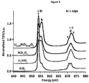
- Fig. 3 presents a comparison of the Ni L-edge XAS for several nickel oxide-based thin films, corresponding to dipole transitions from Ni 2p to Ni 3d states, including both the 2p 3/2 (LIII) and 2p 1/2 (LII) spin-orbit final states. Due to the direct dipole transition from 2p to 3d orbitals and the high resolution in the soft x-ray regime, L-edge XAS of transition metals is sensitive not only to the valency of the metal, but also to the detailed energetics of the ligand-3d interactions governed in particular by symmetry, as well as spin and hybridization.
- the transition metal L-edge can be captured by atomic calculations by the introduction of crystal field effects. It is believed that the XAS spectrum for a NiO x film produced by RF magnetron sputtering closely resembled previously reported data for nickel oxide films. Here, the NiO x XAS spectrum represented transitions from Ni (2p 6 3d 8 ) to Ni (2p 5 3d 9 ), where the final state as probed by XAS was well described by atomic multiplet calculations for a single Ni 2+ in an octahedral coordination ( Fig. 3 ). Upon Li and Zr doping, the high-energy feature b (and e for the LIII edge) was significantly enhanced.
- a nickel oxide-based electrode containing Li/W additives was prepared utilizing identical sputter deposition conditions as used for Li 2.34 NiZr 0.28 O x .
- a chemical formula of Li 1.81 NiW 0.21 O x was determined by ICP-MS.
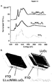
- the film thickness and crystal structure of the Li 1.81 NiW 0.21 O x film were identical to the Li 2.34 NiZr 0.28 O x film ( Fig. 5 ).
- the XAS spectrum for Li 1.81 NiW 0.21 O x demonstrated a similar co-doping effect as observed in Li 2.34 NiZr 0.28 O x ( Fig. 6 ) .
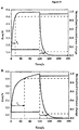
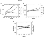
- Cyclic voltammetry and in-situ transmittance curves for Li 2.34 NiZr 0.28 O x and Li 1.81 NiW 0.21 O x thin film electrodes cycled in a 1 M LiClO 4 dissolved in propylene carbonate are shown in Figs. 7a and 7b .
- the charge capacities (determined from the CVs) are 21.8 mC/cm 2 and 21.4 mC/cm 2 for the Li 2.34 NiZr 0.28 O x and Li 1.81 NiW 0.21 O x electrodes, respectively.
- the charge capacities for Li 2.34 NiZr 0.28 O x and Li 1.81 NiW 0.21 O x it is believed, could be controlled (modified) easily by varying the film thickness.
- the in-situ optical modulation at about 670 nm for the Li 2.34 NiZr 0.28 O x film was about 45% compared to about 35% for the Li 1.81 NiW 0.21 O x film.
- the high specific optical density (defined as the optical density per micrometer) for the Li 2.34 NiZr 0.28 O x film (8.1 ⁇ m -1 ) was comparable to that of the state-of-the-art porous WO 3 film (9.0 ⁇ m -1 ).
- a high specific optical density enables a reduction in film thickness without compromising optical contrast properties, therefore reducing manufacturing costs.
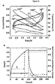
- a thicker Li 2.34 NiZr 0.28 O x film (about 200 nm) showed significantly improved optical modulation (about 72% at 670 nm) while maintaining an optimal bleached state transparency ( Fig. 8 ).
- the coloration efficiencies of Li 2.34 NiZr 0.28 O x and Li 1.81 NiW 0.21 O x at 670 nm are ca. 33 cm 2 /C and ca. 31 cm 2 /C, respectively.
- the bleached state of Li 2.34 NiZr 0.28 O x film was more transparent than that of Li 1.81 NiW 0.21 O x film.
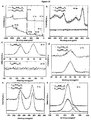
- Fig. 7c provides the UV-vis-NIR spectra (300-1500 nm) for the as-deposited, bleached and dark films.
- the as-deposited films showed similar optical characteristics except that the Li 2.34 NiZr 0.28 O x film had higher transmittance especially for irradiation wavelengths less than about 400 nm.
- the transmittance of nickel oxide films typically decreased when the irradiation wavelength was less than 800 nm. However, the decrease did not occur in the bleached state of the Li 2.34 NiZr 0.28 O x film. A significantly larger contrast in the bleached-state transparency was observed for the Li 2.34 NiZr 0.28 O x film in the UV-vis region relative to the Li 1.81 NiW 0.21 O x film.
- the b* values for the bleached states of Li 2.34 NiZr 0.28 O x and Li 1.81 NiW 0.21 O x were estimated to be about 6.5 and about 12.6, respectively.
- a b* value below 8 was typically undetectable by the human eye indicating that the bleached-state for Li 2.34 NiZr 0.28 O x was nearly colorless (no remnant yellow color, Fig. 7d ).
- the bleached-state transmittance of Li 2.34 NiZr 0.28 O x was highly improved in the near infrared region. This improved transparency across the spectrum allowed for more efficient control of solar heat gain and natural light harnessing.
- Electrochromic processes in nickel oxide anodic electrodes are typically slower than in cathodic WO x electrodes and, it is believed, impede the overall switching kinetics of a layered electrochromic device.
- Wet-chemical synthesis routes have been employed to fabricate porous nickel oxide structures in order to reduce the switching time from one state to another state.
- Improved optical switching has also been observed in modified nickel oxide films synthesized using conventional sputter techniques.
- the normalized in-situ transmittance changes under potential step cycling are shown in Figs. 9a and 9b , for Li 2.34 NiZr 0.28 O x and Li 1.81 NiW 0.21 O x , respectively.
- the switching speed was defined as the time required to achieve about 90% of transmittance change upon a potential step.
- the bleaching and coloration kinetics were both greatly improved for the Li 2.34 NiZr 0.28 O x film, with bleaching (T b ) and coloration (T c ) times of about 18 seconds and about 20 seconds, respectively.
- the T b and T c times for Li 1.81 NiW 0.21 O x were 61 seconds and 31 seconds, respectively.
- the interface between an electrochromic film and electrolyte plays a crucial role in facilitating the efficient insertion and removal of lithium.
- the surface composition of the nickel oxide-based electrodes was probed with X-ray photoelectron spectroscopy (XPS) and O K-edge XAS. As shown in Fig. 10 , the XPS spectra for Li 2.34 NiZr 0.28 O x and Li 1.81 NiW 0.21 O x clearly demonstrated that the surface composition of the modified nickel-oxide films depended on the metal additives (Li/Zr vs. Li/W). High-resolution XPS identified every element (i.e., Li, Ni, W and O) present in the Li 1.81 NiW 0.21 O x film.
- the highly improved electrochromic performance in the Li 2.34 NiZr 0.28 O x electrode is also associated with the uniqueness of the composition of the multicomponent films.
- Figs. 12 and 13 compare the in-situ optical modulation and switching kinetics of NiZr x O y and Li x NiO y . In general, without in-situ lithiation, the optical modulation for NiZr x O y would be exceedingly reduced and the bleached-state transparency would be significantly improved when Zr is present, presumable in the form of ZrO 2 .
- Ni L-edge soft X-rays
- Fig. 14b A XAS study of the bulk electronic structure of nickel oxide electronic structure (i.e., Ni K-edge) is shown in Fig. 14b .
- the pre-edge feature at ca. 8332 eV was attributed to the transition from Ni 1s to the hybridization state of Ni 3d and O 2p, and it was an indication of oxidation state for the target Ni atom. There are clear shifts in the pre-edge energy and pre-edge absorption between the dark and bleached samples, indicating the formal change of the Ni oxidation state.
- the electrochromic mechanism could be associated with a reversible transformation of formal Ni oxidation states, which was closely related to the well-known Bode mechanism.
- the observed changes in Ni L-edge spectrum indicated that the formal increase of nickel oxidation state was not simply associated with a change from Ni 2+ to Ni 3+ , but that the increased hole concentration was more localized on the neighboring oxygen, which then impacted the Ni oxidation states through the Ni 3d-O 2p hybridization state.
- An identical Ni K-edge and Ni L-edge XAS study of Li 1.81 NiW 0.21 O x confirmed that this mechanism was applicable for various nickel oxide-based anodic electrodes in Li-ion electrolytes ( Fig. 15 ).
- CE materials described herein and the methods of depositing these materials allows for high-quality electrochromic films and tunable control of material composition and structure. It is believed that the addition of Li/Zr additives to nickel oxide was found to yield a superior performing electrochromic material in terms of optical modulation, bleached-state transparency and switching kinetics relative to the resulting nickel oxide material with Li/W additives. It is believed that the high specific optical density of Li 2.34 NiZr 0.28 O x allows for increased manufacturability. It is believed that the electrochromic effect in multi-component nickel oxide-based materials arises from the reversible formation of hole states that are localized on the neighboring oxygen orbitals.
- Figure 2c shows an expanded NiO(II) nanocrystal lattice structure for Li 2.34 NiZr 0.28 O x from High Resolution Cross Sectional Transmission Electron Microscopy (HRXTEM).
- the micrograph also reveals that the nanocrystal size is approximately 5 nm.
- Figure 16 illustrates the increase in NiO(II) nanocrystal size with higher nickel concentrations (Li0.0 Ni(II) 0.5 Ni (III) 0.5 W 0.25 O 2.25 compared to Li 0.0 Ni(II) 0.5 Ni(III) 0.5 W 0.2 O 2.25 from X-ray diffraction. Essentially, it is believed that increasing the nickel to tungsten ratio from about 1:0.33 to about 1:0.25, without lithium, increased the NiO(II) nanocrystal size from about 7nm to about 9nm.
- Table 1 below illustrates how the amount of surface nickel varies with nano-crystal size.
- Figure 1 depicts a nano-crystal with about equal amounts of core and surface material.
- Table 1 Nano-crystal Diameter, nm Nano-crystal Core Volume, nm ⁇ 3 Nano-crystal Surface Volume, nm ⁇ 3 Nano-crystal Surface/Core Ratio 2.1 1 6 5.39 2.7 3 9 2.92 3.4 8 15 1.77 4.6 27 28 1.01 5.8 62 44 0.70 7.3 138 69 0.50 9.1 300 110 0.37 10.5 467 144 0.31 11.5 637 175 0.27 12.4 810 203 0.25
- Ni(III) dark Ni(III) and bleached Ni(II) is likely to proceed both reversibly and to stoichiometric completion (complete conversion).
Claims (14)
- Dispositif électrochrome comprenant :(a) une première électrode comprenant une couche parmi une couche électrochrome ou une couche de contre-électrode,(b) une seconde électrode comprenant l'autre couche parmi ladite couche électrochrome ou ladite couche de contre-électrode,(c) une couche conductrice d'ions pour conduire des ions entre lesdites première et seconde électrodes,(d) une première couche conductrice, et(e) une seconde couche conductrice,lesdites première et seconde électrodes et ladite couche conductrice d'ions étant prises en sandwich entre lesdites première et seconde couches conductrices,
ladite couche de contre-électrode comprenant au moins un oxyde mixte ayant la formule LixNi(II)(1-y)Ni(III)(y)M(A)zO(1+0,5x+0,5y+2z), où M est un métal, où A est l'état d'oxydation du métal M et x vaut de 1 à 4, y vaut de 0,1 à 1, z vaut de 0,05 à 2 et où M(A) est choisi dans le groupe constitué par Si(IV), Ti(IV), Mn(IV), Zr(IV), Sn(IV), Ce(IV), Hf(IV), Re(IV) et Ir(IV). - Dispositif électrochrome comprenant :(a) une première électrode comprenant une couche parmi une couche électrochrome ou une couche de contre-électrode,(b) une seconde électrode comprenant l'autre couche parmi ladite couche électrochrome ou ladite couche de contre-électrode,(c) une couche conductrice d'ions pour conduire des ions entre lesdites première et seconde électrodes,(d) une première couche conductrice, et(e) une seconde couche conductrice,lesdites première et seconde électrodes et ladite couche conductrice d'ions étant prises en sandwich entre lesdites première et seconde couches conductrices,
ladite couche de contre-électrode comprenant au moins un oxyde mixte ayant la formule LixNi(II)(1-y)Ni(III)(y)M(A)zO(1+0,5x+0,5y+2,5z), où M est un métal, où A est l'état d'oxydation du métal M et x vaut de 1 à 4, y vaut de 0,1 à 1, z vaut de 0,05 à 2 et où M(A) est choisi dans le groupe constitué de V(V), Nb(V), Sb(V), Ta(V) et Pa(V). - Dispositif électrochrome comprenant :(a) une première électrode comprenant une couche parmi une couche électrochrome ou une couche de contre-électrode,(b) une seconde électrode comprenant l'autre couche parmi ladite couche électrochrome ou ladite couche de contre-électrode,(c) une couche conductrice d'ions pour conduire des ions entre lesdites première et seconde électrodes,(d) une première couche conductrice, et(e) une seconde couche conductrice,lesdites première et seconde électrodes et ladite couche conductrice d'ions étant prises en sandwich entre lesdites première et seconde couches conductrices,
ladite couche de contre-électrode comprenant au moins un oxyde mixte ayant la formule Li x Ni(II) (1-y) Ni(III) (y) M(A) z O (1+0,5x+0,5y+3z) , où M est un métal, où A est l'état d'oxydation du métal M et x vaut de 1 à 4, y vaut de 0,1 à 1, z vaut de 0,05 à 2, où M(A) est choisi dans le groupe constitué par Cr(VI), Se(VI), Mo(VI), Te(VI) et W(VI). - Dispositif électrochrome selon la revendication 1, dans lequel ledit oxyde mixte est Li2,3Ni(II)(0,5)Ni(III)(0,5)Zr(IV)0,3O3,25.
- Dispositif électrochrome selon la revendication 1, dans lequel ledit oxyde mixte est Li2,3Ni(II)(0,5)Ni(III)(0,5)Hf(IV)0,3O3,25.
- Dispositif électrochrome selon la revendication 1, dans lequel ledit oxyde mixte est Li2,3Ni(II)(0,5)Ni(III)(0,5)Zr(IV)0,294Hf(IV)0,006O3,25.
- Dispositif électrochrome selon la revendication 1, dans lequel ledit oxyde mixte est en outre dopé avec un métal ou un oxyde métallique supplémentaire.
- Dispositif électrochrome selon la revendication 1, dans lequel une épaisseur de ladite couche de contre-électrode est comprise dans la plage allant de 80 nm à 500 nm.
- Dispositif électrochrome selon la revendication 8, dans lequel ladite épaisseur est comprise dans la plage allant de 100 nm à 320 nm.
- Dispositif électrochrome selon la revendication 1, dans lequel ledit oxyde mixte est sensiblement amorphe.
- Procédé de préparation d'un dispositif électrochrome selon l'une quelconque des revendications précédentes, le procédé comprenant :(a) la fourniture d'une première couche conductrice,(b) le dépôt d'une couche parmi une couche électrochrome ou une couche de contre-électrode sur ladite première couche conductrice, fournissant ainsi une première électrode déposée,(c) le dépôt d'une couche conductrice d'ions sur ladite première électrode déposée,(d) le dépôt de l'autre couche parmi ladite couche électrochrome ou ladite couche de contre-électrode sur ladite couche conductrice d'ions, fournissant ainsi une seconde électrode déposée,(e) le dépôt d'une seconde couche conductrice sur ladite seconde électrode déposée.
- Procédé selon la revendication 11, comprenant en outre le dépôt de lithium dans l'une de ladite couche conductrice d'ions ou de ladite couche de contre-électrode.
- Procédé selon la revendication 11, dans lequel ladite contre-électrode est déposée par pulvérisation réactive par magnétron en courant continu.
- Unité de vitrage isolée comprenant le dispositif électrochrome selon les revendications 1 à 3.
Applications Claiming Priority (2)
| Application Number | Priority Date | Filing Date | Title |
|---|---|---|---|
| US201161510381P | 2011-07-21 | 2011-07-21 | |
| PCT/US2012/047569 WO2013013135A1 (fr) | 2011-07-21 | 2012-07-20 | Oxyde de nickel électrochromique dopé simultanément avec du lithium et un dopant métallique |
Publications (2)
| Publication Number | Publication Date |
|---|---|
| EP2734601A1 EP2734601A1 (fr) | 2014-05-28 |
| EP2734601B1 true EP2734601B1 (fr) | 2019-09-04 |
Family
ID=46639675
Family Applications (1)
| Application Number | Title | Priority Date | Filing Date |
|---|---|---|---|
| EP12744150.9A Active EP2734601B1 (fr) | 2011-07-21 | 2012-07-20 | Oxyde de nickel électrochromique dopé simultanément avec du lithium et un dopant métallique |
Country Status (6)
| Country | Link |
|---|---|
| US (5) | US8687261B2 (fr) |
| EP (1) | EP2734601B1 (fr) |
| JP (1) | JP6067010B2 (fr) |
| KR (1) | KR101933370B1 (fr) |
| CN (2) | CN103814107B (fr) |
| WO (1) | WO2013013135A1 (fr) |
Families Citing this family (62)
| Publication number | Priority date | Publication date | Assignee | Title |
|---|---|---|---|---|
| WO2015168166A1 (fr) * | 2014-05-02 | 2015-11-05 | View, Inc. | Fabrication de dispositifs électrochromes à faible défectivité |
| US10591795B2 (en) | 2009-03-31 | 2020-03-17 | View, Inc. | Counter electrode for electrochromic devices |
| US8582193B2 (en) | 2010-04-30 | 2013-11-12 | View, Inc. | Electrochromic devices |
| US8432603B2 (en) | 2009-03-31 | 2013-04-30 | View, Inc. | Electrochromic devices |
| US10852613B2 (en) | 2009-03-31 | 2020-12-01 | View, Inc. | Counter electrode material for electrochromic devices |
| US9261751B2 (en) | 2010-04-30 | 2016-02-16 | View, Inc. | Electrochromic devices |
| US10156762B2 (en) | 2009-03-31 | 2018-12-18 | View, Inc. | Counter electrode for electrochromic devices |
| US10261381B2 (en) | 2009-03-31 | 2019-04-16 | View, Inc. | Fabrication of low defectivity electrochromic devices |
| US11187954B2 (en) | 2009-03-31 | 2021-11-30 | View, Inc. | Electrochromic cathode materials |
| US9759975B2 (en) | 2010-04-30 | 2017-09-12 | View, Inc. | Electrochromic devices |
| US8780432B1 (en) * | 2011-03-22 | 2014-07-15 | Paul Phong Nguyen | Electrochromic devices and methods for forming such devices |
| PL2737530T3 (pl) * | 2011-07-25 | 2018-12-31 | The Regents Of The University Of California | Nanokompozytowe warstwy elektrochromatyczne |
| CN104040412B (zh) | 2011-10-20 | 2016-01-13 | 奥克利有限公司 | 具有色度增强的眼镜 |
| WO2013169987A1 (fr) | 2012-05-10 | 2013-11-14 | Oakley, Inc. | Lunettes à couches fonctionnelles stratifiées |
| CN105008992B (zh) * | 2012-08-09 | 2018-01-09 | Sage电致变色显示有限公司 | 用于电致变色器件的三元镍氧化物材料 |
| DK2946246T3 (da) * | 2013-01-21 | 2019-07-01 | Kinestral Tech Inc | Flerlags elektrokrom indretning med lithium-nikkel-oxid-baseret anode |
| US20140205746A1 (en) * | 2013-01-21 | 2014-07-24 | Kinestral Technologies, Inc. | Process for preparing a multi-layer electrochromic structure |
| US9207514B2 (en) * | 2013-01-21 | 2015-12-08 | Kinestral Technologies, Inc. | Electrochromic lithium nickel group 4 mixed metal oxides |
| US9360729B2 (en) | 2013-03-15 | 2016-06-07 | Kinestral Technologies, Inc. | Electrochromic lithium nickel group 6 mixed metal oxides |
| WO2015034437A1 (fr) * | 2013-09-03 | 2015-03-12 | Nanyang Technological University | Matériau nanostructuré d'oxyde métallique et dispositifs électrochromiques contenant le matériau |
| US9575335B1 (en) | 2014-01-10 | 2017-02-21 | Oakley, Inc. | Eyewear with chroma enhancement for specific activities |
| US10767143B2 (en) * | 2014-03-06 | 2020-09-08 | Sage Electrochromics, Inc. | Particle removal from electrochromic films using non-aqueous fluids |
| WO2015153337A1 (fr) * | 2014-04-01 | 2015-10-08 | The Regents Of The University Of California | Matériau électrochromique nanostructuré d'oxyde métallique de transition conducteur et dispositifs de commutation optique constitués de ceux-ci |
| US11891327B2 (en) | 2014-05-02 | 2024-02-06 | View, Inc. | Fabrication of low defectivity electrochromic devices |
| CN113448133A (zh) * | 2014-05-02 | 2021-09-28 | 唯景公司 | 电致变色装置 |
| US10429713B2 (en) | 2014-06-12 | 2019-10-01 | Gentex Corporation | Selectively-transparent electrochromic display |
| US9939702B2 (en) * | 2014-06-17 | 2018-04-10 | Sage Electrochromics, Inc. | Controlled switching for electrochromic devices |
| US10061177B2 (en) | 2014-07-23 | 2018-08-28 | Kinestral Technologies, Inc. | Process for preparing multi-layer electrochromic stacks |
| US10670936B2 (en) * | 2014-07-23 | 2020-06-02 | Kinestral Technologies, Inc. | Wet-coating of thin film lithium nickel oxides for electrochromic applications |
| CN112327556A (zh) | 2014-09-05 | 2021-02-05 | 唯景公司 | 用于电致变色装置的反电极 |
| JPWO2016063849A1 (ja) | 2014-10-21 | 2017-08-10 | 旭硝子株式会社 | 光学素子および撮像装置 |
| CN207704150U (zh) | 2014-11-13 | 2018-08-07 | 奥克利有限公司 | 具有颜色增强的可变光衰减眼睛佩戴件 |
| US9791760B2 (en) | 2014-11-14 | 2017-10-17 | Heliotrope Technologies, Inc. | Electrochromic device containing metal oxide nanoparticles and ultraviolet blocking material |
| EP3224670B1 (fr) | 2014-11-26 | 2023-04-12 | View, Inc. | Contre-électrode pour dispositifs électrochromiques |
| RU2700361C2 (ru) * | 2014-11-26 | 2019-09-16 | Вью, Инк. | Противоэлектрод для электрохромных устройств |
| KR20230014842A (ko) * | 2014-12-19 | 2023-01-30 | 뷰, 인크. | 부스 바 하에 있는 전기변색 디바이스에서의 결함들을 완화시키는 방법 |
| EP3341788A4 (fr) | 2015-08-26 | 2019-02-13 | Heliotrope Technologies, Inc. | Dispositif électrochromique contenant des nanostructures à couleur réglable |
| US9684219B2 (en) | 2015-08-26 | 2017-06-20 | Heliotrope Technologies | Electrochromic device containing color-tunable nanostructures |
| KR101999978B1 (ko) * | 2015-09-25 | 2019-07-15 | 주식회사 엘지화학 | 전기변색소자의 제조방법 |
| WO2017059364A1 (fr) * | 2015-10-02 | 2017-04-06 | Heliotrope Technologies, Inc. | Dispositif électrochrome contenant un réflecteur de bragg distribué configuré pour sélectivement réfléchir un rayonnement uv |
| US10766422B2 (en) * | 2015-12-11 | 2020-09-08 | Gentex Corporation | IR transmitting coating for electro-optic element |
| KR102108553B1 (ko) * | 2016-03-31 | 2020-05-08 | 주식회사 엘지화학 | 전기변색소자 |
| KR102108562B1 (ko) * | 2016-03-31 | 2020-05-08 | 주식회사 엘지화학 | 전기변색소자 |
| US20190146294A1 (en) * | 2016-04-28 | 2019-05-16 | Board Of Regents, The University Of Texas System | Electrochromic electrodes and methods of making and use thereof |
| WO2017218705A1 (fr) | 2016-06-17 | 2017-12-21 | View, Inc. | Atténuation des défauts dans un dispositif électrochrome sous une barre omnibus |
| CN106290529B (zh) * | 2016-08-04 | 2018-12-25 | 北京工业大学 | 一种基于多循环双阶跃计时分析技术的电致变色材料循环稳定性测试及分析方法 |
| US10295821B2 (en) | 2016-08-19 | 2019-05-21 | Oakley, Inc. | Laminated lenses with anti-fogging functionality |
| US11099449B1 (en) * | 2016-08-30 | 2021-08-24 | Kinestral Technologies, Inc. | EC devices with nanostructred thin film anodes |
| US10331003B2 (en) * | 2016-09-26 | 2019-06-25 | Heliotrope Technologies, Inc. | Electrochromic privacy window |
| WO2019014776A1 (fr) * | 2017-07-20 | 2019-01-24 | Curtis Berlinguette | Photodéposition d'oxydes métalliques pour dispositifs électrochromes |
| KR102118358B1 (ko) | 2017-09-18 | 2020-06-04 | 주식회사 엘지화학 | 전기변색소자의 제조방법 |
| KR102152623B1 (ko) | 2017-10-26 | 2020-09-09 | 한국전자통신연구원 | 표시소자 및 그 제조방법 |
| US11112622B2 (en) | 2018-02-01 | 2021-09-07 | Luxottica S.R.L. | Eyewear and lenses with multiple molded lens components |
| US11866647B2 (en) | 2018-07-18 | 2024-01-09 | Comberry, Llc | Electrochromic material and method of manufacturing thereof |
| EP3830640A4 (fr) | 2018-07-31 | 2022-04-06 | Sage Electrochromics, Inc. | Dispositifs électrochimiques et ses procédés de formation |
| CN109148826B (zh) * | 2018-09-12 | 2021-05-25 | 桑德新能源技术开发有限公司 | 一种负极及其制备方法、锂电池 |
| CN109298579A (zh) * | 2018-12-07 | 2019-02-01 | 哈尔滨工业大学 | 一种全固态电致变色器件及其制备方法 |
| US11703737B2 (en) * | 2020-02-12 | 2023-07-18 | Sage Electrochromics, Inc. | Forming electrochromic stacks using at most one metallic lithium deposition station |
| CN112198731A (zh) * | 2020-08-31 | 2021-01-08 | 基迈克材料科技(苏州)有限公司 | 电致变色膜系及电致变色器件 |
| JP7379306B2 (ja) * | 2020-09-28 | 2023-11-14 | 東芝マテリアル株式会社 | エレクトロクロミック素子 |
| CN113419391B (zh) * | 2021-06-04 | 2022-03-15 | 中国航发北京航空材料研究院 | 一种高电荷存储量的电致变色对电极的制备方法 |
| CN113774343A (zh) * | 2021-08-10 | 2021-12-10 | 北京航空航天大学 | 一种电致变色掺杂薄膜的新型共溅射制备方法 |
Family Cites Families (23)
| Publication number | Priority date | Publication date | Assignee | Title |
|---|---|---|---|---|
| KR100271537B1 (ko) | 1992-04-10 | 2000-11-15 | 존 이. 밴 다인 | 전자크롬장치 및 그 제조방법 |
| US5277986A (en) | 1992-07-15 | 1994-01-11 | Donnelly Corporation | Method for depositing high performing electrochromic layers |
| US5668663A (en) | 1994-05-05 | 1997-09-16 | Donnelly Corporation | Electrochromic mirrors and devices |
| FR2746934B1 (fr) * | 1996-03-27 | 1998-05-07 | Saint Gobain Vitrage | Dispositif electrochimique |
| FR2762876B1 (fr) | 1997-03-03 | 2002-03-22 | Luk Fahrzeug Hydraulik | Compresseur notamment pour la climatisation d'un vehicule automobile |
| US6094292A (en) | 1997-10-15 | 2000-07-25 | Trustees Of Tufts College | Electrochromic window with high reflectivity modulation |
| FR2793888B1 (fr) | 1999-05-20 | 2002-06-28 | Saint Gobain Vitrage | Dispositif electrochimique |
| DE60136703D1 (de) * | 2000-05-04 | 2009-01-08 | Schott Donnelly Llc | Verfahren zur Herstellung einer electrochromen Tafel |
| JP4707028B2 (ja) * | 2000-09-29 | 2011-06-22 | シャープ株式会社 | リチウム二次電池 |
| US6859297B2 (en) | 2001-08-07 | 2005-02-22 | Midwest Research Institute | Electrochromic counter electrode |
| AU2002362016B2 (en) * | 2001-11-21 | 2007-01-25 | University Of Florida | Electrochromic polymers and polymer electrochromic devices |
| US7914946B2 (en) | 2004-06-15 | 2011-03-29 | Fuelcell Energy, Inc. | Cathode side hardware for carbonate fuel cells |
| US7372610B2 (en) | 2005-02-23 | 2008-05-13 | Sage Electrochromics, Inc. | Electrochromic devices and methods |
| CN1290795C (zh) * | 2005-04-29 | 2006-12-20 | 北京科技大学 | 一种锂钛共掺杂氧化镍基陶瓷薄膜及其制备方法 |
| KR100860452B1 (ko) | 2005-12-13 | 2008-09-25 | 주식회사 엘지화학 | 활성화된 금속산화물의 제조방법 |
| TWI367385B (en) * | 2006-01-09 | 2012-07-01 | Lg Chemical Ltd | Electrode comprising lithium nickel oxide layer, method for preparing the same, and electrochromic device comprising the same |
| US7830585B2 (en) | 2006-11-09 | 2010-11-09 | Sage Electrochromics, Inc. | Method of making an ion-switching device without a separate lithiation step |
| WO2008091099A1 (fr) * | 2007-01-22 | 2008-07-31 | Lg Chem, Ltd. | Électrodes comprenant une couche d'oxyde lithium nickel, son procédé de préparation et dispositif électrochromique la comprenant |
| US20090057137A1 (en) | 2007-08-31 | 2009-03-05 | Midwest Research Institute | Synthesizing thin films of lithiated transition metal oxide for use in electrochemical and battery devices |
| US8643930B2 (en) * | 2007-08-31 | 2014-02-04 | Alliance For Sustainable Energy, Llc | Thin film lithium-based batteries and electrochromic devices fabricated with nanocomposite electrode materials |
| CN101441938A (zh) * | 2008-11-26 | 2009-05-27 | 南京航空航天大学 | 适用于大电流充/放电工作条件的电化学电容器 |
| US8432603B2 (en) | 2009-03-31 | 2013-04-30 | View, Inc. | Electrochromic devices |
| CN105008992B (zh) | 2012-08-09 | 2018-01-09 | Sage电致变色显示有限公司 | 用于电致变色器件的三元镍氧化物材料 |
-
2012
- 2012-07-20 US US13/554,144 patent/US8687261B2/en active Active
- 2012-07-20 WO PCT/US2012/047569 patent/WO2013013135A1/fr active Application Filing
- 2012-07-20 JP JP2014521820A patent/JP6067010B2/ja active Active
- 2012-07-20 KR KR1020147004337A patent/KR101933370B1/ko active IP Right Grant
- 2012-07-20 CN CN201280046248.0A patent/CN103814107B/zh active Active
- 2012-07-20 CN CN201710580279.9A patent/CN107300819B/zh active Active
- 2012-07-20 EP EP12744150.9A patent/EP2734601B1/fr active Active
-
2013
- 2013-09-19 US US14/031,573 patent/US9651845B2/en active Active
-
2017
- 2017-04-05 US US15/479,942 patent/US10514581B2/en active Active
-
2019
- 2019-11-20 US US16/689,799 patent/US11520204B2/en active Active
-
2022
- 2022-10-31 US US18/051,309 patent/US20230168557A1/en active Pending
Non-Patent Citations (1)
| Title |
|---|
| None * |
Also Published As
| Publication number | Publication date |
|---|---|
| KR20140068026A (ko) | 2014-06-05 |
| CN107300819A (zh) | 2017-10-27 |
| JP6067010B2 (ja) | 2017-01-25 |
| CN107300819B (zh) | 2021-03-12 |
| WO2013013135A1 (fr) | 2013-01-24 |
| US20130182307A1 (en) | 2013-07-18 |
| US8687261B2 (en) | 2014-04-01 |
| EP2734601A1 (fr) | 2014-05-28 |
| CN103814107B (zh) | 2017-08-04 |
| US11520204B2 (en) | 2022-12-06 |
| US20200089071A1 (en) | 2020-03-19 |
| JP2014521128A (ja) | 2014-08-25 |
| US10514581B2 (en) | 2019-12-24 |
| US9651845B2 (en) | 2017-05-16 |
| KR101933370B1 (ko) | 2018-12-31 |
| US20230168557A1 (en) | 2023-06-01 |
| US20140016173A1 (en) | 2014-01-16 |
| US20170269449A1 (en) | 2017-09-21 |
| CN103814107A (zh) | 2014-05-21 |
Similar Documents
| Publication | Publication Date | Title |
|---|---|---|
| US11520204B2 (en) | Electrochromic nickel oxide simultaneously doped with lithium and a metal dopant | |
| US20230176439A1 (en) | Electrochromic devices and methods | |
| JP5232159B2 (ja) | 独立したリチオ化ステップを含まないイオン−スイッチング装置の製法 | |
| Granqvist et al. | Recent advances in electrochromics for smart windows applications | |
| US11866647B2 (en) | Electrochromic material and method of manufacturing thereof | |
| US20230311463A1 (en) | Tungsten oxide nanostructure thin films for electrochromic devices | |
| Chen et al. | Photoelectrochemical performance of a UV-cured all-solid-state complementary ITO/WO3/Ta2O5/electrolyte/NiO/ITO electrochromic device deposited by ion-beam assisted electron-beam evaporation | |
| Veszelei et al. | Optical and electrochemical properties of Li+ intercalated Zr–Ce oxide and Hf–Ce oxide films | |
| US10877347B1 (en) | Thin film lithium tungsten oxides for electrochromic applications and methods of making the same |
Legal Events
| Date | Code | Title | Description |
|---|---|---|---|
| PUAI | Public reference made under article 153(3) epc to a published international application that has entered the european phase |
Free format text: ORIGINAL CODE: 0009012 |
|
| 17P | Request for examination filed |
Effective date: 20140220 |
|
| AK | Designated contracting states |
Kind code of ref document: A1 Designated state(s): AL AT BE BG CH CY CZ DE DK EE ES FI FR GB GR HR HU IE IS IT LI LT LU LV MC MK MT NL NO PL PT RO RS SE SI SK SM TR |
|
| DAX | Request for extension of the european patent (deleted) | ||
| STAA | Information on the status of an ep patent application or granted ep patent |
Free format text: STATUS: EXAMINATION IS IN PROGRESS |
|
| 17Q | First examination report despatched |
Effective date: 20171206 |
|
| GRAP | Despatch of communication of intention to grant a patent |
Free format text: ORIGINAL CODE: EPIDOSNIGR1 |
|
| STAA | Information on the status of an ep patent application or granted ep patent |
Free format text: STATUS: GRANT OF PATENT IS INTENDED |
|
| INTG | Intention to grant announced |
Effective date: 20190410 |
|
| GRAS | Grant fee paid |
Free format text: ORIGINAL CODE: EPIDOSNIGR3 |
|
| GRAA | (expected) grant |
Free format text: ORIGINAL CODE: 0009210 |
|
| STAA | Information on the status of an ep patent application or granted ep patent |
Free format text: STATUS: THE PATENT HAS BEEN GRANTED |
|
| AK | Designated contracting states |
Kind code of ref document: B1 Designated state(s): AL AT BE BG CH CY CZ DE DK EE ES FI FR GB GR HR HU IE IS IT LI LT LU LV MC MK MT NL NO PL PT RO RS SE SI SK SM TR |
|
| REG | Reference to a national code |
Ref country code: GB Ref legal event code: FG4D |
|
| REG | Reference to a national code |
Ref country code: CH Ref legal event code: EP |
|
| REG | Reference to a national code |
Ref country code: AT Ref legal event code: REF Ref document number: 1175332 Country of ref document: AT Kind code of ref document: T Effective date: 20190915 |
|
| REG | Reference to a national code |
Ref country code: DE Ref legal event code: R096 Ref document number: 602012063630 Country of ref document: DE |
|
| REG | Reference to a national code |
Ref country code: IE Ref legal event code: FG4D |
|
| REG | Reference to a national code |
Ref country code: NL Ref legal event code: FP |
|
| REG | Reference to a national code |
Ref country code: LT Ref legal event code: MG4D |
|
| PG25 | Lapsed in a contracting state [announced via postgrant information from national office to epo] |
Ref country code: BG Free format text: LAPSE BECAUSE OF FAILURE TO SUBMIT A TRANSLATION OF THE DESCRIPTION OR TO PAY THE FEE WITHIN THE PRESCRIBED TIME-LIMIT Effective date: 20191204 Ref country code: LT Free format text: LAPSE BECAUSE OF FAILURE TO SUBMIT A TRANSLATION OF THE DESCRIPTION OR TO PAY THE FEE WITHIN THE PRESCRIBED TIME-LIMIT Effective date: 20190904 Ref country code: HR Free format text: LAPSE BECAUSE OF FAILURE TO SUBMIT A TRANSLATION OF THE DESCRIPTION OR TO PAY THE FEE WITHIN THE PRESCRIBED TIME-LIMIT Effective date: 20190904 Ref country code: SE Free format text: LAPSE BECAUSE OF FAILURE TO SUBMIT A TRANSLATION OF THE DESCRIPTION OR TO PAY THE FEE WITHIN THE PRESCRIBED TIME-LIMIT Effective date: 20190904 Ref country code: NO Free format text: LAPSE BECAUSE OF FAILURE TO SUBMIT A TRANSLATION OF THE DESCRIPTION OR TO PAY THE FEE WITHIN THE PRESCRIBED TIME-LIMIT Effective date: 20191204 Ref country code: FI Free format text: LAPSE BECAUSE OF FAILURE TO SUBMIT A TRANSLATION OF THE DESCRIPTION OR TO PAY THE FEE WITHIN THE PRESCRIBED TIME-LIMIT Effective date: 20190904 |
|
| PG25 | Lapsed in a contracting state [announced via postgrant information from national office to epo] |
Ref country code: AL Free format text: LAPSE BECAUSE OF FAILURE TO SUBMIT A TRANSLATION OF THE DESCRIPTION OR TO PAY THE FEE WITHIN THE PRESCRIBED TIME-LIMIT Effective date: 20190904 Ref country code: ES Free format text: LAPSE BECAUSE OF FAILURE TO SUBMIT A TRANSLATION OF THE DESCRIPTION OR TO PAY THE FEE WITHIN THE PRESCRIBED TIME-LIMIT Effective date: 20190904 Ref country code: GR Free format text: LAPSE BECAUSE OF FAILURE TO SUBMIT A TRANSLATION OF THE DESCRIPTION OR TO PAY THE FEE WITHIN THE PRESCRIBED TIME-LIMIT Effective date: 20191205 Ref country code: RS Free format text: LAPSE BECAUSE OF FAILURE TO SUBMIT A TRANSLATION OF THE DESCRIPTION OR TO PAY THE FEE WITHIN THE PRESCRIBED TIME-LIMIT Effective date: 20190904 Ref country code: LV Free format text: LAPSE BECAUSE OF FAILURE TO SUBMIT A TRANSLATION OF THE DESCRIPTION OR TO PAY THE FEE WITHIN THE PRESCRIBED TIME-LIMIT Effective date: 20190904 |
|
| REG | Reference to a national code |
Ref country code: AT Ref legal event code: MK05 Ref document number: 1175332 Country of ref document: AT Kind code of ref document: T Effective date: 20190904 |
|
| PG25 | Lapsed in a contracting state [announced via postgrant information from national office to epo] |
Ref country code: PT Free format text: LAPSE BECAUSE OF FAILURE TO SUBMIT A TRANSLATION OF THE DESCRIPTION OR TO PAY THE FEE WITHIN THE PRESCRIBED TIME-LIMIT Effective date: 20200106 Ref country code: RO Free format text: LAPSE BECAUSE OF FAILURE TO SUBMIT A TRANSLATION OF THE DESCRIPTION OR TO PAY THE FEE WITHIN THE PRESCRIBED TIME-LIMIT Effective date: 20190904 Ref country code: IT Free format text: LAPSE BECAUSE OF FAILURE TO SUBMIT A TRANSLATION OF THE DESCRIPTION OR TO PAY THE FEE WITHIN THE PRESCRIBED TIME-LIMIT Effective date: 20190904 Ref country code: EE Free format text: LAPSE BECAUSE OF FAILURE TO SUBMIT A TRANSLATION OF THE DESCRIPTION OR TO PAY THE FEE WITHIN THE PRESCRIBED TIME-LIMIT Effective date: 20190904 Ref country code: AT Free format text: LAPSE BECAUSE OF FAILURE TO SUBMIT A TRANSLATION OF THE DESCRIPTION OR TO PAY THE FEE WITHIN THE PRESCRIBED TIME-LIMIT Effective date: 20190904 Ref country code: PL Free format text: LAPSE BECAUSE OF FAILURE TO SUBMIT A TRANSLATION OF THE DESCRIPTION OR TO PAY THE FEE WITHIN THE PRESCRIBED TIME-LIMIT Effective date: 20190904 |
|
| PG25 | Lapsed in a contracting state [announced via postgrant information from national office to epo] |
Ref country code: IS Free format text: LAPSE BECAUSE OF FAILURE TO SUBMIT A TRANSLATION OF THE DESCRIPTION OR TO PAY THE FEE WITHIN THE PRESCRIBED TIME-LIMIT Effective date: 20200224 Ref country code: SK Free format text: LAPSE BECAUSE OF FAILURE TO SUBMIT A TRANSLATION OF THE DESCRIPTION OR TO PAY THE FEE WITHIN THE PRESCRIBED TIME-LIMIT Effective date: 20190904 Ref country code: SM Free format text: LAPSE BECAUSE OF FAILURE TO SUBMIT A TRANSLATION OF THE DESCRIPTION OR TO PAY THE FEE WITHIN THE PRESCRIBED TIME-LIMIT Effective date: 20190904 Ref country code: CZ Free format text: LAPSE BECAUSE OF FAILURE TO SUBMIT A TRANSLATION OF THE DESCRIPTION OR TO PAY THE FEE WITHIN THE PRESCRIBED TIME-LIMIT Effective date: 20190904 |
|
| REG | Reference to a national code |
Ref country code: DE Ref legal event code: R097 Ref document number: 602012063630 Country of ref document: DE |
|
| PLBE | No opposition filed within time limit |
Free format text: ORIGINAL CODE: 0009261 |
|
| STAA | Information on the status of an ep patent application or granted ep patent |
Free format text: STATUS: NO OPPOSITION FILED WITHIN TIME LIMIT |
|
| PG2D | Information on lapse in contracting state deleted |
Ref country code: IS |
|
| PG25 | Lapsed in a contracting state [announced via postgrant information from national office to epo] |
Ref country code: DK Free format text: LAPSE BECAUSE OF FAILURE TO SUBMIT A TRANSLATION OF THE DESCRIPTION OR TO PAY THE FEE WITHIN THE PRESCRIBED TIME-LIMIT Effective date: 20190904 Ref country code: IS Free format text: LAPSE BECAUSE OF FAILURE TO SUBMIT A TRANSLATION OF THE DESCRIPTION OR TO PAY THE FEE WITHIN THE PRESCRIBED TIME-LIMIT Effective date: 20200105 |
|
| 26N | No opposition filed |
Effective date: 20200605 |
|
| PG25 | Lapsed in a contracting state [announced via postgrant information from national office to epo] |
Ref country code: SI Free format text: LAPSE BECAUSE OF FAILURE TO SUBMIT A TRANSLATION OF THE DESCRIPTION OR TO PAY THE FEE WITHIN THE PRESCRIBED TIME-LIMIT Effective date: 20190904 |
|
| PG25 | Lapsed in a contracting state [announced via postgrant information from national office to epo] |
Ref country code: MC Free format text: LAPSE BECAUSE OF FAILURE TO SUBMIT A TRANSLATION OF THE DESCRIPTION OR TO PAY THE FEE WITHIN THE PRESCRIBED TIME-LIMIT Effective date: 20190904 |
|
| PG25 | Lapsed in a contracting state [announced via postgrant information from national office to epo] |
Ref country code: LU Free format text: LAPSE BECAUSE OF NON-PAYMENT OF DUE FEES Effective date: 20200720 |
|
| PG25 | Lapsed in a contracting state [announced via postgrant information from national office to epo] |
Ref country code: IE Free format text: LAPSE BECAUSE OF NON-PAYMENT OF DUE FEES Effective date: 20200720 |
|
| PG25 | Lapsed in a contracting state [announced via postgrant information from national office to epo] |
Ref country code: TR Free format text: LAPSE BECAUSE OF FAILURE TO SUBMIT A TRANSLATION OF THE DESCRIPTION OR TO PAY THE FEE WITHIN THE PRESCRIBED TIME-LIMIT Effective date: 20190904 Ref country code: MT Free format text: LAPSE BECAUSE OF FAILURE TO SUBMIT A TRANSLATION OF THE DESCRIPTION OR TO PAY THE FEE WITHIN THE PRESCRIBED TIME-LIMIT Effective date: 20190904 Ref country code: CY Free format text: LAPSE BECAUSE OF FAILURE TO SUBMIT A TRANSLATION OF THE DESCRIPTION OR TO PAY THE FEE WITHIN THE PRESCRIBED TIME-LIMIT Effective date: 20190904 |
|
| PG25 | Lapsed in a contracting state [announced via postgrant information from national office to epo] |
Ref country code: MK Free format text: LAPSE BECAUSE OF FAILURE TO SUBMIT A TRANSLATION OF THE DESCRIPTION OR TO PAY THE FEE WITHIN THE PRESCRIBED TIME-LIMIT Effective date: 20190904 |
|
| P01 | Opt-out of the competence of the unified patent court (upc) registered |
Effective date: 20230530 |
|
| PGFP | Annual fee paid to national office [announced via postgrant information from national office to epo] |
Ref country code: NL Payment date: 20230622 Year of fee payment: 12 Ref country code: FR Payment date: 20230621 Year of fee payment: 12 |
|
| PGFP | Annual fee paid to national office [announced via postgrant information from national office to epo] |
Ref country code: BE Payment date: 20230622 Year of fee payment: 12 |
|
| PGFP | Annual fee paid to national office [announced via postgrant information from national office to epo] |
Ref country code: GB Payment date: 20230620 Year of fee payment: 12 Ref country code: CH Payment date: 20230801 Year of fee payment: 12 |
|
| PGFP | Annual fee paid to national office [announced via postgrant information from national office to epo] |
Ref country code: DE Payment date: 20230620 Year of fee payment: 12 |
|
| REG | Reference to a national code |
Ref country code: DE Ref legal event code: R082 Ref document number: 602012063630 Country of ref document: DE Representative=s name: KRAUS & LEDERER PARTGMBB, DE |