EP2723147A1 - Method for inspecting electronic device and electronic device inspection apparatus - Google Patents
Method for inspecting electronic device and electronic device inspection apparatus Download PDFInfo
- Publication number
- EP2723147A1 EP2723147A1 EP12800543.6A EP12800543A EP2723147A1 EP 2723147 A1 EP2723147 A1 EP 2723147A1 EP 12800543 A EP12800543 A EP 12800543A EP 2723147 A1 EP2723147 A1 EP 2723147A1
- Authority
- EP
- European Patent Office
- Prior art keywords
- electronic device
- inspection
- electronic devices
- roll
- substrate
- Prior art date
- Legal status (The legal status is an assumption and is not a legal conclusion. Google has not performed a legal analysis and makes no representation as to the accuracy of the status listed.)
- Withdrawn
Links
Images





Classifications
-
- G—PHYSICS
- G01—MEASURING; TESTING
- G01R—MEASURING ELECTRIC VARIABLES; MEASURING MAGNETIC VARIABLES
- G01R31/00—Arrangements for testing electric properties; Arrangements for locating electric faults; Arrangements for electrical testing characterised by what is being tested not provided for elsewhere
- G01R31/01—Subjecting similar articles in turn to test, e.g. "go/no-go" tests in mass production; Testing objects at points as they pass through a testing station
-
- G—PHYSICS
- G01—MEASURING; TESTING
- G01R—MEASURING ELECTRIC VARIABLES; MEASURING MAGNETIC VARIABLES
- G01R1/00—Details of instruments or arrangements of the types included in groups G01R5/00 - G01R13/00 and G01R31/00
- G01R1/02—General constructional details
-
- G—PHYSICS
- G02—OPTICS
- G02F—OPTICAL DEVICES OR ARRANGEMENTS FOR THE CONTROL OF LIGHT BY MODIFICATION OF THE OPTICAL PROPERTIES OF THE MEDIA OF THE ELEMENTS INVOLVED THEREIN; NON-LINEAR OPTICS; FREQUENCY-CHANGING OF LIGHT; OPTICAL LOGIC ELEMENTS; OPTICAL ANALOGUE/DIGITAL CONVERTERS
- G02F1/00—Devices or arrangements for the control of the intensity, colour, phase, polarisation or direction of light arriving from an independent light source, e.g. switching, gating or modulating; Non-linear optics
- G02F1/01—Devices or arrangements for the control of the intensity, colour, phase, polarisation or direction of light arriving from an independent light source, e.g. switching, gating or modulating; Non-linear optics for the control of the intensity, phase, polarisation or colour
- G02F1/13—Devices or arrangements for the control of the intensity, colour, phase, polarisation or direction of light arriving from an independent light source, e.g. switching, gating or modulating; Non-linear optics for the control of the intensity, phase, polarisation or colour based on liquid crystals, e.g. single liquid crystal display cells
- G02F1/1306—Details
- G02F1/1309—Repairing; Testing
-
- G—PHYSICS
- G09—EDUCATION; CRYPTOGRAPHY; DISPLAY; ADVERTISING; SEALS
- G09G—ARRANGEMENTS OR CIRCUITS FOR CONTROL OF INDICATING DEVICES USING STATIC MEANS TO PRESENT VARIABLE INFORMATION
- G09G3/00—Control arrangements or circuits, of interest only in connection with visual indicators other than cathode-ray tubes
- G09G3/006—Electronic inspection or testing of displays and display drivers, e.g. of LED or LCD displays
-
- H—ELECTRICITY
- H02—GENERATION; CONVERSION OR DISTRIBUTION OF ELECTRIC POWER
- H02S—GENERATION OF ELECTRIC POWER BY CONVERSION OF INFRARED RADIATION, VISIBLE LIGHT OR ULTRAVIOLET LIGHT, e.g. USING PHOTOVOLTAIC [PV] MODULES
- H02S50/00—Monitoring or testing of PV systems, e.g. load balancing or fault identification
- H02S50/10—Testing of PV devices, e.g. of PV modules or single PV cells
-
- H—ELECTRICITY
- H10—SEMICONDUCTOR DEVICES; ELECTRIC SOLID-STATE DEVICES NOT OTHERWISE PROVIDED FOR
- H10K—ORGANIC ELECTRIC SOLID-STATE DEVICES
- H10K71/00—Manufacture or treatment specially adapted for the organic devices covered by this subclass
- H10K71/70—Testing, e.g. accelerated lifetime tests
-
- H—ELECTRICITY
- H10—SEMICONDUCTOR DEVICES; ELECTRIC SOLID-STATE DEVICES NOT OTHERWISE PROVIDED FOR
- H10P—GENERIC PROCESSES OR APPARATUS FOR THE MANUFACTURE OR TREATMENT OF DEVICES COVERED BY CLASS H10
- H10P74/00—Testing or measuring during manufacture or treatment of wafers, substrates or devices
- H10P74/27—Structural arrangements therefor
-
- G—PHYSICS
- G09—EDUCATION; CRYPTOGRAPHY; DISPLAY; ADVERTISING; SEALS
- G09G—ARRANGEMENTS OR CIRCUITS FOR CONTROL OF INDICATING DEVICES USING STATIC MEANS TO PRESENT VARIABLE INFORMATION
- G09G3/00—Control arrangements or circuits, of interest only in connection with visual indicators other than cathode-ray tubes
- G09G3/20—Control arrangements or circuits, of interest only in connection with visual indicators other than cathode-ray tubes for presentation of an assembly of a number of characters, e.g. a page, by composing the assembly by combination of individual elements arranged in a matrix no fixed position being assigned to or needed to be assigned to the individual characters or partial characters
- G09G3/22—Control arrangements or circuits, of interest only in connection with visual indicators other than cathode-ray tubes for presentation of an assembly of a number of characters, e.g. a page, by composing the assembly by combination of individual elements arranged in a matrix no fixed position being assigned to or needed to be assigned to the individual characters or partial characters using controlled light sources
- G09G3/30—Control arrangements or circuits, of interest only in connection with visual indicators other than cathode-ray tubes for presentation of an assembly of a number of characters, e.g. a page, by composing the assembly by combination of individual elements arranged in a matrix no fixed position being assigned to or needed to be assigned to the individual characters or partial characters using controlled light sources using electroluminescent panels
- G09G3/32—Control arrangements or circuits, of interest only in connection with visual indicators other than cathode-ray tubes for presentation of an assembly of a number of characters, e.g. a page, by composing the assembly by combination of individual elements arranged in a matrix no fixed position being assigned to or needed to be assigned to the individual characters or partial characters using controlled light sources using electroluminescent panels semiconductive, e.g. using light-emitting diodes [LED]
- G09G3/3208—Control arrangements or circuits, of interest only in connection with visual indicators other than cathode-ray tubes for presentation of an assembly of a number of characters, e.g. a page, by composing the assembly by combination of individual elements arranged in a matrix no fixed position being assigned to or needed to be assigned to the individual characters or partial characters using controlled light sources using electroluminescent panels semiconductive, e.g. using light-emitting diodes [LED] organic, e.g. using organic light-emitting diodes [OLED]
-
- Y—GENERAL TAGGING OF NEW TECHNOLOGICAL DEVELOPMENTS; GENERAL TAGGING OF CROSS-SECTIONAL TECHNOLOGIES SPANNING OVER SEVERAL SECTIONS OF THE IPC; TECHNICAL SUBJECTS COVERED BY FORMER USPC CROSS-REFERENCE ART COLLECTIONS [XRACs] AND DIGESTS
- Y02—TECHNOLOGIES OR APPLICATIONS FOR MITIGATION OR ADAPTATION AGAINST CLIMATE CHANGE
- Y02E—REDUCTION OF GREENHOUSE GAS [GHG] EMISSIONS, RELATED TO ENERGY GENERATION, TRANSMISSION OR DISTRIBUTION
- Y02E10/00—Energy generation through renewable energy sources
- Y02E10/50—Photovoltaic [PV] energy
- Y02E10/542—Dye sensitized solar cells
Definitions
- the present invention relates to a method for inspecting an electronic device and an electronic device inspection apparatus.
- the roll-to-roll system which has higher productivity than that of the batch production and the single sheet production is also desired in the above inspection process of electronic devices.
- each of the electronic devices is actually conveyed intermittently to be inspected.
- there is a technique of intermittently conveying, in the longer direction, a tape-shaped thin film successively formed of a plurality of film substrates on which semiconductor chips are mounted and performing functional verification for each of the semiconductor chips see patent document 1, for example.
- the inspection process is normally performed by the intermittent inspection of single sheet or roll-to-roll, which does not sufficiently make use of merits of high productivity of the roll-to-roll system.
- the apparatus as in the above patent document 3 used for the conductive sheet cannot be used and positioning of the conduction unit is necessary, and thus intermittent inspection has to be performed even when the electronic device is produced by the single sheet or the roll-to-roll.
- the inspection process requires time and it is impossible to make use of merits of high productivity when producing the electronic device by the roll-to-roll system.
- the present invention was made in consideration of the above matters and an object of the present invention is to provide a method for inspecting an electronic device and an electronic device inspection apparatus which can perform a rapid and 100-percent inspection of electrical characteristics of the electronic device continuously conveyed by the roll-to-roll system and can make use of merits of high productivity.
- the invention of claim 1 is characterized in performing electric conduction to the electronic device by using a conduction unit to carry out an inspection of an electrical characteristic while the electronic device is being continuously conveyed.
- the invention of claim 2 is characterized in that, in the method for inspecting the electronic device of claim 1, the inspection of the electrical characteristic is carried out by the conduction unit and the electronic device continuously contacting each other to perform the electric conduction in a state where the conduction unit is fixed.
- the invention of claim 3 is characterized in that, in the method for inspecting the electronic device of claim 1, the inspection of the electrical characteristic is carried out by synchronizing the conduction unit with conveyance of the electronic device so that the conduction unit and the electronic device continuously contact each other to perform the electric conduction.
- the invention of claim 4 is characterized in that, in the method for inspecting the electronic device of any one of claims 1 to 3, a plurality of the electronic devices are provided on a substrate and conveyed.
- the invention of claim 5 is characterized in that, in the method for inspecting the electronic device of any one of claims 1 to 4, a substrate is a resin film, a metal foil or a glass.
- the invention of claim 6 is characterized in that, in the method for inspecting the electronic device of any one of claims 1 to 5, the electronic device is an organic electronic device.
- the invention of claim 7 is characterized in that, in the method for inspecting the electronic device of any one of claims 1 to 6, the inspection of the electrical characteristic is carried out by detecting luminescence from the electronic device due to the electric conduction.
- the invention of claim 8 is characterized in comprising: a conveying unit which continuously conveys an electronic device; a conduction unit which performs electric conduction to the electronic device which is continuously conveyed by the conveying unit; and an electrical characteristic inspection unit which carries out an inspection of an electrical characteristic of the electronic device to which the electric conduction is performed by the conduction unit.
- a rapid and 100-percent electrical characteristic inspection of electronic device can be performed on electronic devices which are continuously conveyed by the roll-to-roll system, and thus it is possible to make use of the merits of high productivity.
- FIG. 1 is an external schematic view of electronic devices and an electronic device inspection apparatus.
- the electronic device is a display element, a light, a primary cell, a secondary cell, a solar cell, a non-volatile memory and a switching element, for example, and a preferable one among them is a printed electronic device such as an organic electroluminescence panel (hereinafter, called an organic EL panel), an organic thin-film solar cell, a dye-sensitized solar cell, an electronic paper, a secondary cell or an organic TFT.
- an organic electroluminescence panel hereinafter, called an organic EL panel
- an organic thin-film solar cell an organic thin-film solar cell
- a dye-sensitized solar cell an electronic paper
- secondary cell a secondary cell or an organic TFT.
- a plurality of electronic devices 1 are provided on a long substrate 100.
- Each of the electronic devices 1 is in a nearly rectangle in a plan view extending in the longer direction of the substrate 100. Then, the electronic devices 1 are provided in two lines in the width direction with predetermined intervals along the longer direction on the substrate 100.
- An electrode 10 (anode 2 and cathode 7) is formed on each of the electronic devices 1.
- the anode 2 is formed on a side edge portion and the cathode 7 is formed on the other side edge portion in the longer direction of each of the electronic devices 1. That is, the anodes 2 of the electronic devices 1 are located in lines along the longer direction and the cathodes 7 of the electronic devices 1 are also located in lines along the longer direction.
- the substrate 100 for example, a resin film, a metal foil and a glass are suggested and a long flexible material is especially preferable.
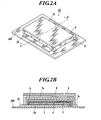
- FIG. 2A is a schematic view showing a schematic configuration of an organic EL panel and FIG. 2B is a schematic sectional view of FIG. 2A cut along the line A-A.
- an organic EL panel 1a includes an anode 2a, a hole transport layer 3, a luminescent layer 4, an electron transport layer 5, a cathode buffer layer (electron injection layer) 6, a cathode 7a, an adhesive layer 8 and a sealing member 9 in order on the substrate 100.
- the anode 2a is formed of ITO including an oxide of indium and tin, for example.
- An organic functional layer is formed of the hole transport layer 3, the luminescent layer 4, the electron transport layer 5 and the cathode buffer layer 6.
- the organic functional layer can be configured by including at least the luminescent layer 4. By conducting electrical current to such organic functional layer (luminescent layer 4), the luminescent material inside the luminescent layer 4 emits light.
- a sealing layer is formed of the adhesive layer 8 and the sealing member 9.
- the cathode 7a is formed of an inorganic material such as aluminum, for example.
- the organic EL panel 1a indicates a state where the cathode 7a is sealed with the sealing member 9 via the adhesive layer 8, and the organic EL element indicates a state where the components up to the cathode 7a are formed.
- an electronic device inspection apparatus 20 is an apparatus of inspecting electrical characteristics by continuously conducting electrical current to the plurality of electronic devices 1 on the substrate 100 which is continuously conveyed by the roll-to-roll system after forming the plurality of electronic devices 1 on the substrate 100 by the roll-to-roll system and before packaging the electronic devices 1.
- the organic functional layer (luminescent layer 4) emits light by the electrical current passing between the anode 2a and the cathode 7a, and the electrical characteristics are inspected.
- the electrical characteristic inspection is performed by inspecting luminescence (ultraviolet light, visible light and infrared light) from the electronic device 1 by the electric conduction.
- the electrical characteristic inspection includes IV inspection (current-voltage test), IVL inspection (current-voltage luminance test), light emission luminance inspection, inspection of dark spot and bright spot (luminescent spot), leakage inspection, unevenness inspection, color temperature, defect inspection and such like.
- the electronic device inspection apparatus 20 includes a conveying unit 30 which continuously conveys the substrate 100 provided with a plurality of electronic devices 1, a conducting roll 40 for conducting electrical current to the electronic devices 1 of the substrate 100 conveyed by the conveying unit 30 and an electrical characteristic inspection unit 50 for inspecting electrical characteristics of the electronic devices 1.
- the conveying unit 30 includes a delivery roll 31 which delivers the substrate 100 provided with the plurality of electronic devices 1, a guide roll 32 which supports the delivered substrate 100, a wind-up roll (not shown in the drawings) which winds up the substrate 100 after inspection, and a driving source (not shown in the drawings) such as a motor which drives the delivery roll 31, the guide roll 32 and the wind-up roll, for example.
- the conducting roll 40 is provided in a state of being fixed between the guide roll 32 and the wind-up roll.
- the conducting roll 40 is rotatable to support the conveyed substrate 100 at the surface and deliver the conveyed substrate 100 in the conveyance direction.
- an electrode 41 is formed as a conduction unit with respect to the electrodes 10 (anodes 2 and cathodes 7) of the electronic devices 1 (see FIG. 3A ).
- the conveyed substrate 100 is supported on the surface of the conducting roll 40, and electrical current is conducted by the electrodes 10 of the electronic devices 1 contacting the electrode 41 (see FIG. 3A ) which is formed on the surface of the conducting roll 40.
- FIG. 3A is an external schematic view showing the electrode of the conducting roll
- FIG. 3B is an enlarged view of an electrode portion of the conducting roll.
- positive electrodes 42 and negative electrodes 43 of the electrode 41 of the conducting roll 40 are located alternately in the width direction of the conducting roll 40 so as to correspond to the electrodes 10 (anodes 2 and cathodes 7) of the electronic devices 1.
- grooves 44 are formed in four lines in the width direction along the circumferential direction on the surface of the conducting roll 40. Then, as shown in FIG. 3B , the electrode 41 is configured by providing a plurality of pin probes 45 of the positive electrode 42 or the negative electrode 43 in each of the grooves 44.
- the pin probes 45 are connected to a feed circuit not shown in the drawings, electrical current is conducted to the pin probes 45 via the feed circuit and electrical current passes through the electronic devices 1 when the electrodes 10 of the electronic devices 1 contact the pin probes 45.
- the electrical current passes through the organic functional layer (luminescent layer 4) of the organic EL panel 1a to emit light.
- the location of the electrode 41 (positive electrodes 42 and negative electrodes 43) of the conducting roll 40 is not limited to the above-mentioned example, and the electrode 41 is provided so as to correspond to the location of the electrodes 10 (anodes 2 and cathodes 7) of the electronic devices 1.
- FIGS. 4 to 6 are examples of the shape of the electronic device 1 and location of the electrode 10 of the electronic device 1, for example.
- FIGS. 4 to 6 show an electrical conducting state of the electronic device and the conducting roll.
- the conducting roll and the electronic devices are shown in a schematic view and a plan view, respectively, to make the electrodes of the conducting roll and the electronic devices understandable.
- each of the electronic devices 1 is in a nearly rectangle in a plan view as in FIG. 1 , the electronic devices 1 are provided in a line in the width direction of the substrate 100 with predetermined intervals along the longer direction. Then, the anode 2 is formed on one side edge portion in the longer direction of each of the electronic devices 1 and the cathode 7 is formed on the other side edge portion.
- the electrode 41 of the conducting roll 40 is provided in two lines in the width direction, the positive electrode 42 is formed along the circumferential direction of the conducting roll 40 at the position corresponding to the anode 2 of the electronic device 1, and the negative electrode 43 is formed along the circumferential direction of the conducting roll 40 at the position corresponding to the cathode 7 of the electronic device 1. Accordingly, by the substrate 100 being conveyed, the electrode 10 of the electronic device 1 contacts the corresponding electrode 41 of the conducting roll 40.
- each of the electronic devices 1 is in a nearly square shape in a plan view, and the plurality of electronic devices 1 are provided in a line in the width direction of the substrate 100 with predetermined intervals along the longer direction. Then, the anodes 2 and the cathodes 7 are formed on the four side edge portions of each of the electronic devices 1 so as to face each other. That is, the anodes 2 of each of the electronic devices 1 are located in a line along the longer direction and the cathodes 7 of each of the electronic devices 1 are also located in a line along the longer direction.
- the negative electrodes 43 of the conducting roll 40 are provided in two lines in the width direction and formed at positions corresponding to the negative electrodes 7 of the electronic device 1 along the circumferential direction of the conducting roll 40.
- the positive electrodes 42 are provided between the two lines of negative electrodes 43 so as to extend along the width direction at positions corresponding to the positive electrodes 2 of the electronic device 1. Accordingly, by the substrate 100 being conveyed, the electrode 10 of the electronic device 1 contacts the corresponding electrode 41 of the conducting roll 40.
- each of the electronic devices 1 is formed in a nearly rectangle in a plan view and the electronic devices 1 are provided in two lines in the width direction of the substrate 100 with predetermined intervals along the longer direction. Then, the cathode 7, the positive electrode 2 and the cathode 7 are located in this order with predetermined intervals on each of the side edge portions in the longer direction of each of the electronic devices 1.
- the electrodes 41 of the conducting roll 40 are provided in four lines in the width direction in each of which the positive electrodes 42 and the negative electrodes 43 are alternately located along the circumferential direction of the conducting roll 40 so as to correspond to the electrode 10 (anode 2 and cathodes 7) of the electronic device 1. Therefore, by the substrate 100 being conveyed, the electrodes 10 of the electronic devices 1 contact the corresponding electrodes 41 of the conducting roll 40.
- the electrode 41 of the conducting roll 40 is configured by forming grooves 44 on the surface of the conducting roll 40 and providing a plurality of pin probes 45 of positive electrode 42 or negative electrode 43 in each of the grooves 44 as in FIGS. 3A and 3B .
- the electronic device inspection apparatus 20 includes a positioning unit 60 which moves the substrate 100 in the width direction of the substrate 100 to perform positioning in the width direction so that a predetermined electrode 41 of the conducting roll 40 contacts the corresponding electrodes 10 of the electronic devices 1.
- the positioning unit 60 includes an EPC sensor 61 (edge position control sensor), an amplifier unit 62 and a position control unit 63, for example.
- the EPC sensor 61 is provided near the upstream side of the conducting roll 40 so as to detect the movement of the edge position in the width direction of the substrate 100 and output the edge position information to the amplifier unit 62.
- the amplifier unit 62 is connected to the position control unit 63.
- the position control unit 63 moves the delivery roll 31 in the width direction to move the position in the width direction of the substrate 100 and controls so that the electrodes 10 of the electronic device 1 contact the corresponding electrode 41 of the conducting roll 40.
- a photodetector such as a line sensor which detects light emitted from the electronic device 1 can be used in a case of performing light emission luminance inspection, unevenness inspection and defect inspection.
- IVL inspection can be performed by arranging a plurality of sets of conducting roll 40 and line sensor with predetermined intervals and applying a different amount of current to the conducting rolls 40 to perform luminance measurement, for example.
- the electrical characteristic inspection can be performed by providing the electrical characteristic inspection unit 50 with a mechanism of following the conveyed substrate for a predetermined distance so as to follow the device to be measured during the measurement.
- voltage value (or current value) and luminance can be measured with respect to the applied current value (or voltage value) by using a luminance meter (for example, CA-2000 made by Konica Minolta Sensing).
- the leakage inspection can be performed by detecting infrared light with an infrared camera (for example, SC325 and SC5600-M made by FLIR, and C10633-34 made by Hamamatsu Photonics) or by detecting weak luminescence with a highly sensitive CCD camera (for, example, SI-CCD made by Hamamatsu Photonics).
- the color temperature can be inspected by using the luminance meter.
- the delivery roll 31, the guide roll 32 and the wind-up roll rotate to convey the substrate 100.
- the conveyed substrate 100 is supported by the conducting roll 40, and the predetermined electrode 41 of the conducting roll 40 sequentially contacts the corresponding electrodes 10 of the electronic devices 1.
- the current is conducted and the electrical characteristic inspection is performed.
- the electronic device 1 is the organic EL panel 1a
- the current passes through the organic functional layer (luminescent layer 4) of the organic EL panel 1a to emit light, and the electrical characteristics such as light emission luminance are inspected by a photodetector and such like which is the electrical characteristic inspection unit 50.
- the current is continuously conducted to each of the electronic devices 1 on the conducting roll 40 and the electrical characteristic inspection is sequentially performed.
- the EPC sensor 61 detects the position of the edge in the width direction of the substrate 100 and outputs the information of the edge position to the amplifier unit 62, and the position control unit 63 connected to the amplifier unit 62 controls the position in the width direction of the substrate 100 so that the corresponding electrodes 10 of the electronic devices 1 contact the electrode 41 of the conducting roll 40 on the basis of the information of the edge position.
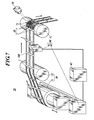
- FIG. 7 is an external schematic view showing a modification example of the electronic device and the electronic device inspection apparatus of FIG. 1 .
- an electronic device inspection apparatus 70 shown in FIG. 7 is configured so that the conduction unit contacts the electronic devices 1 from above.
- the conducting roll 40 of FIG. 1 is replaced with a guide roll 71 not having the electrode 41, and a probe 72 which is a conduction unit is provided above the guide roll 71 in a state of being fixed.
- the probe 72 is provided so as to contact the positions corresponding to the anodes 2 and the cathodes 7 of the electronic devices 1 on the conveyed substrate 100.
- the probe 72 is connected to the feed circuit which is not shown in the drawings and the electrical current is conducted to the probe 72 via the feed circuit.
- the substrate 100 conveyed by the conveying unit 30 is supported by the guide roll 71 and the corresponding electrodes 10 of the electronic devices 1 sequentially contact the probe 72.
- the current is continuously conducted to perform electrical characteristic inspection.
- the other unit such as the conveying unit 30, the electrical characteristic inspection unit 50 and the positioning unit 60 are similar to those in a case of FIG. 1 , the explanation thereof is omitted.
- FIG. 8 is an external schematic view showing a modification example of the electronic device and the electronic device inspection apparatus of FIG. 1 .
- FIG. 9A is a side view of FIG. 8 seen from the B direction and
- FIG. 9B is an external schematic view of an electrode plate.
- the conduction unit is synchronized with the conveyance of the electronic devices 1 (substrate 100) and conducts electrical current to the predetermined electrodes 10 of the electronic devices 1 to perform the electrical characteristic inspection.
- the electronic device inspection apparatus 80 is located below (on the back surface side) the substrate 100.
- the electronic device inspection apparatus 80 includes a pair of bases 81 and 81 which extend along the longer direction of the substrate 100 and are horizontally movable with respect to the conveyance direction of the substrate 100, a first stage 82 which is provided on one of the bases 81 so as to move up and down, a second stage 83 which is provided on the other base 81 so as to move up and down, and first and second electrode plates 84 and 85 which are provided on the first and second stages 82 and 83, respectively.
- the pair of bases 81 and 81 is located under the substrate 100 so that the bases 81 and 81 are parallel to each other.
- electrode patterns (conduction unit) 86 are formed on the upper face (surface) of the first electrode plate 84 so as to correspond to the electrodes 10 of the electronic devices 1. Also, suction units 87 which suck the lower surfaces (back surfaces) of the electronic devices 1 are formed on the upper surface of the first electrode plate 84.
- the suction units 87 include suction ports 871, a suction pump (not shown in the drawings) connected to the suction ports 871 and such like, and the suction ports are absorbed to the lower surfaces of the electronic devices 1 by the suction pump being driven.
- the electrode patterns (conduction unit) 86 and the suction units 87 are also formed on the upper surface of the second electrode plate 85 similarly to the first electrode plate 84.
- the position of the suction units 87 is not limited to that of FIG. 9B , and changes can be appropriately made as long as the electronic devices 1 can be sucked.
- the first stage 82 and the second stage 83 move up and down while alternately moving in the horizontal direction so that the first and second electrode plates 84 and 85 contact the electrodes 10 of the predetermined electronic devices 1 to conduct electricity.
- the first stage 82 is elevated while moving in the horizontal direction so that the first electrode plate 84 contacts the lower surfaces of the electronic devices 1 to conduct electrical current and inspection is performed.
- the second stage 83 horizontally moves to a predetermined position in the conveyance direction of the next electronic devices 1 nearest to the upstream in the conveyance direction.
- the first stage 82 is lowered to be away from the electronic devices 1 and the second stage 83 is elevated so that the second electrode plate 85 contacts the lower surfaces of the next electronic devices 1 nearest to the upstream in the conveyance direction to conduct electrical current and inspection is performed.
- the first stage 82 horizontally moves to a predetermined position in the conveyance direction of the next electronic devices 1 nearest to the upstream in the conveyance direction.
- the electrical current is continuously conducted between the first and second electrode plates 84 and 85 and the electrodes 10 of the predetermined electronic devices 1, and inspection is performed.
- FIG. 10 is an external schematic view showing a modification example of the electronic device and the electronic device inspection apparatus of FIG. 1 .
- the conduction unit conducts electrical current to the predetermined electrodes 10 of the electronic devices 1 in synchronization with the conveyance of the electronic devices 1 (substrate 100) to perform the electrical characteristic inspection.
- the electronic device inspection apparatus 90 is located in a side of the substrate 100.
- the electronic device inspection apparatus 90 includes a main body 91, a driving source (not shown in the drawings) such as a motor provided on the main body 91, a plurality of driving rollers (not shown in the drawings) which rotate being driven by the motor, a rotating belt 92 wound up by the driving rollers, a plurality of stages 93 which are provided on the surface of the rotating belt 92 so as to move up and down, and electrode plates 94 which are provided on the stages 93.
- a driving source such as a motor provided on the main body 91
- a plurality of driving rollers (not shown in the drawings) which rotate being driven by the motor
- a rotating belt 92 wound up by the driving rollers
- stages 93 which are provided on the surface of the rotating belt 92 so as to move up and down
- electrode plates 94 which are provided on the stages 93.
- the plurality of stages 93 are provided on the surface of the rotating belt 92 with predetermined intervals along the circumferential direction.
- the stages 93 are rotated by the rotating belt 92 and are sequentially elevated and lowered along the rotation direction.
- Electrode patterns (conduction unit) 95 are formed on the upper surface (surface) of each of the electrode plates 94 so as to correspond to the electrodes 10 of the electronic devices 1 as in the above FIG. 9B . Also, suction units (not shown in the drawings) sucking the lower surfaces (back surfaces) of the electronic devices 1 may be formed on the upper surface of the electrode plate 94 as in FIG. 9B .
- the stage 93 located at a predetermined position is elevated so that the electrode plate 94 thereof contacts the lower surfaces of the electronic devices 1 to conduct electrical current and inspection is performed.
- the stage 93 is lowered to be away from the electronic devices 1 and rotated by the rotating belt 92.
- the next stage 93 is elevated so that the electrode plate 94 thereof contacts the lower surfaces of the electronic devices 1 to conduct electrical current and the inspection is performed similarly.
- the electrode plate 94 is continuously conducted electrically to the electrodes 10 of the predetermined electronic devices 1 to perform the inspection.
- the electrical characteristic inspection is performed by continuously conducting electrical current to the continuously conveyed electronic devices 1, electrical characteristic inspection of all the electronic devices 1 can be performed rapidly and easily.
- the inspection process can be performed without change and it is possible to make use of the merits of high productivity.
- the present invention can be appropriately used for electronic devices which are continuously conveyed by the roll-to-roll system.
Landscapes
- Physics & Mathematics (AREA)
- General Physics & Mathematics (AREA)
- Engineering & Computer Science (AREA)
- Nonlinear Science (AREA)
- Chemical & Material Sciences (AREA)
- Crystallography & Structural Chemistry (AREA)
- Optics & Photonics (AREA)
- Computer Hardware Design (AREA)
- Theoretical Computer Science (AREA)
- Manufacturing & Machinery (AREA)
- Electroluminescent Light Sources (AREA)
- Testing Of Individual Semiconductor Devices (AREA)
Abstract
Description
- The present invention relates to a method for inspecting an electronic device and an electronic device inspection apparatus.
- Conventionally, electronic devices such as an organic electroluminescence element, a solar cell, a secondary cell and electronic paper have been manufactured by vapor deposition, a wet process (spin coating method, casting method, ink-j et method, spraying method, printing method) and such like (hereinafter, also called a coating method), which have been performed by batch production or single sheet production. Thus, an inspection process of electrical characteristics and such like of the electronic devices has been also performed by the batch or sheet.
- As the inspection process, specifically, there has been known a technique of sequentially receiving an inspection pallet loaded with a plurality of light emitting panels which are set to conduct a current and performing determination of the inspection of electrical and optical characteristics for each of the light emitting panels (for example, see patent document 1).
- However, instead of such batch production and single sheet production, attention has been recently paid to production by a so-called roll-to-roll system of performing coating on a rolled film (continuous flexible substrate) since it facilitates continuous production.
- The roll-to-roll system which has higher productivity than that of the batch production and the single sheet production is also desired in the above inspection process of electronic devices. However, even when produced by the roll-to-roll system, each of the electronic devices is actually conveyed intermittently to be inspected. As an example, there is a technique of intermittently conveying, in the longer direction, a tape-shaped thin film successively formed of a plurality of film substrates on which semiconductor chips are mounted and performing functional verification for each of the semiconductor chips (see
patent document 1, for example). Thus, the inspection process is normally performed by the intermittent inspection of single sheet or roll-to-roll, which does not sufficiently make use of merits of high productivity of the roll-to-roll system. - On the other hand, there is known an apparatus which can appropriately measure the surface resistivity of a conductive sheet by conveying the long conductive sheet, though it is not the electronic devices (see
patent document 3, for example). In such case, since the conductive sheet is used, electricity can pass thoroughly, the current can be conducted easily by a conduction unit contacting appropriate portions of the conductive sheet, and the surface conductivity can be measured. -
- [Patent Document 1] Japanese Patent Application Laid Open Publication No.
2005-249425 - [Patent Document 2] Japanese Patent Application Laid Open Publication No.
2008-89394 - [Patent Document 3] Japanese Patent Application Laid Open Publication No.
H10-26644 - In a case of a conductive sheet as in the above-mentioned
patent document 3, the inspection thereof is possible by the conduction unit contacting the appropriate portions of the conductive sheet; however, in a case where electrodes are provided at specific positions as in an electronic device, the inspection thereof needs positioning of the conduction unit so as to contact the electrodes at the positions specific to the electronic device. - Thus, when inspecting the electronic device, the apparatus as in the
above patent document 3 used for the conductive sheet cannot be used and positioning of the conduction unit is necessary, and thus intermittent inspection has to be performed even when the electronic device is produced by the single sheet or the roll-to-roll. Thus, the inspection process requires time and it is impossible to make use of merits of high productivity when producing the electronic device by the roll-to-roll system. - The present invention was made in consideration of the above matters and an object of the present invention is to provide a method for inspecting an electronic device and an electronic device inspection apparatus which can perform a rapid and 100-percent inspection of electrical characteristics of the electronic device continuously conveyed by the roll-to-roll system and can make use of merits of high productivity.
- In order to achieve the above object, the invention of
claim 1 is characterized in performing electric conduction to the electronic device by using a conduction unit to carry out an inspection of an electrical characteristic while the electronic device is being continuously conveyed. - The invention of
claim 2 is characterized in that, in the method for inspecting the electronic device ofclaim 1, the inspection of the electrical characteristic is carried out by the conduction unit and the electronic device continuously contacting each other to perform the electric conduction in a state where the conduction unit is fixed. - The invention of
claim 3 is characterized in that, in the method for inspecting the electronic device ofclaim 1, the inspection of the electrical characteristic is carried out by synchronizing the conduction unit with conveyance of the electronic device so that the conduction unit and the electronic device continuously contact each other to perform the electric conduction. - The invention of
claim 4 is characterized in that, in the method for inspecting the electronic device of any one ofclaims 1 to 3, a plurality of the electronic devices are provided on a substrate and conveyed. - The invention of
claim 5 is characterized in that, in the method for inspecting the electronic device of any one ofclaims 1 to 4, a substrate is a resin film, a metal foil or a glass. - The invention of
claim 6 is characterized in that, in the method for inspecting the electronic device of any one ofclaims 1 to 5, the electronic device is an organic electronic device. - The invention of
claim 7 is characterized in that, in the method for inspecting the electronic device of any one ofclaims 1 to 6, the inspection of the electrical characteristic is carried out by detecting luminescence from the electronic device due to the electric conduction. - The invention of
claim 8 is characterized in comprising: a conveying unit which continuously conveys an electronic device; a conduction unit which performs electric conduction to the electronic device which is continuously conveyed by the conveying unit; and an electrical characteristic inspection unit which carries out an inspection of an electrical characteristic of the electronic device to which the electric conduction is performed by the conduction unit. - According to the present invention, a rapid and 100-percent electrical characteristic inspection of electronic device can be performed on electronic devices which are continuously conveyed by the roll-to-roll system, and thus it is possible to make use of the merits of high productivity.
-
- [
FIG. 1 ] This is an external schematic view of electronic devices and an electronic device inspection apparatus. - [
FIG. 2A ] This is a schematic view showing a schematic configuration of an organic EL panel. - [
FIG. 2B ] This is a schematic sectional view ofFIG. 2A cut along the line A-A. - [
FIG. 3A ] This is an external schematic view showing electrodes of a conducting roll. - [
FIG. 3B ] This is an enlarged view of an electrode portion of the conducting roll ofFIG. 3A . - [
FIG. 4 ] This is a diagram showing the shape of the electronic device and a location example of the electrodes of the electronic device and the conducting roll. - [
FIG. 5 ] This is a diagram showing the shape of the electronic device and a location example of the electrodes of the electronic device and the conducting roll. - [
FIG. 6 ] This is a diagram showing the shape of the electronic device and a location example of the electrodes of the electronic device and the conducting roll. - [
FIG. 7 ] This is an external schematic view showing a modification example of the electronic devices and the electronic device inspection apparatus ofFIG. 1 . - [
FIG. 8 ] This is an external schematic view showing a modification example of the electronic devices and the electronic device inspection apparatus ofFIG. 1 . - [
FIG. 9A ] This is a side view ofFIG. 8 seen from the B direction. - [
FIG. 9B ] This is an external schematic view of an electrode plate. - [
FIG. 10 ] This is an external schematic view showing a modification example of the electronic devices and the electronic device inspection apparatus ofFIG. 1 . - Hereinafter, an embodiment of the present invention will be described with reference to the drawings.
- First, an electronic device to be used in an inspection method of electronic device of the present invention will be described.
-
FIG. 1 is an external schematic view of electronic devices and an electronic device inspection apparatus. - The electronic device is a display element, a light, a primary cell, a secondary cell, a solar cell, a non-volatile memory and a switching element, for example, and a preferable one among them is a printed electronic device such as an organic electroluminescence panel (hereinafter, called an organic EL panel), an organic thin-film solar cell, a dye-sensitized solar cell, an electronic paper, a secondary cell or an organic TFT.
- As shown in
FIG. 1 , a plurality ofelectronic devices 1 are provided on along substrate 100. Each of theelectronic devices 1 is in a nearly rectangle in a plan view extending in the longer direction of thesubstrate 100. Then, theelectronic devices 1 are provided in two lines in the width direction with predetermined intervals along the longer direction on thesubstrate 100. - An electrode 10 (
anode 2 and cathode 7) is formed on each of theelectronic devices 1. In a case ofFIG. 1 , theanode 2 is formed on a side edge portion and thecathode 7 is formed on the other side edge portion in the longer direction of each of theelectronic devices 1. That is, theanodes 2 of theelectronic devices 1 are located in lines along the longer direction and thecathodes 7 of theelectronic devices 1 are also located in lines along the longer direction. - As the
substrate 100, for example, a resin film, a metal foil and a glass are suggested and a long flexible material is especially preferable. - Hereinafter, the configuration in a case where the electronic device is an organic EL panel will be described.
-
FIG. 2A is a schematic view showing a schematic configuration of an organic EL panel andFIG. 2B is a schematic sectional view ofFIG. 2A cut along the line A-A. - As shown in
FIGS. 2A and 2B , an organic EL panel 1a includes ananode 2a, ahole transport layer 3, aluminescent layer 4, anelectron transport layer 5, a cathode buffer layer (electron injection layer) 6, acathode 7a, anadhesive layer 8 and a sealingmember 9 in order on thesubstrate 100. - The
anode 2a is formed of ITO including an oxide of indium and tin, for example. - An organic functional layer is formed of the
hole transport layer 3, theluminescent layer 4, theelectron transport layer 5 and thecathode buffer layer 6. The organic functional layer can be configured by including at least theluminescent layer 4. By conducting electrical current to such organic functional layer (luminescent layer 4), the luminescent material inside theluminescent layer 4 emits light. In addition, a sealing layer is formed of theadhesive layer 8 and the sealingmember 9. - The
cathode 7a is formed of an inorganic material such as aluminum, for example. - As described above, the organic EL panel 1a indicates a state where the
cathode 7a is sealed with the sealingmember 9 via theadhesive layer 8, and the organic EL element indicates a state where the components up to thecathode 7a are formed. - Next, an electronic device inspection apparatus used in the inspection method of the electronic device of the present invention will be described.
- As shown in
FIG. 1 , an electronicdevice inspection apparatus 20 is an apparatus of inspecting electrical characteristics by continuously conducting electrical current to the plurality ofelectronic devices 1 on thesubstrate 100 which is continuously conveyed by the roll-to-roll system after forming the plurality ofelectronic devices 1 on thesubstrate 100 by the roll-to-roll system and before packaging theelectronic devices 1. - For example, in a case where each of the
electronic devices 1 is the above organic EL panel 1a, the organic functional layer (luminescent layer 4) emits light by the electrical current passing between theanode 2a and thecathode 7a, and the electrical characteristics are inspected. - Here, for example, the electrical characteristic inspection is performed by inspecting luminescence (ultraviolet light, visible light and infrared light) from the
electronic device 1 by the electric conduction. Specifically, the electrical characteristic inspection includes IV inspection (current-voltage test), IVL inspection (current-voltage luminance test), light emission luminance inspection, inspection of dark spot and bright spot (luminescent spot), leakage inspection, unevenness inspection, color temperature, defect inspection and such like. - The electronic
device inspection apparatus 20 includes a conveyingunit 30 which continuously conveys thesubstrate 100 provided with a plurality ofelectronic devices 1, a conductingroll 40 for conducting electrical current to theelectronic devices 1 of thesubstrate 100 conveyed by the conveyingunit 30 and an electricalcharacteristic inspection unit 50 for inspecting electrical characteristics of theelectronic devices 1. - The conveying
unit 30 includes adelivery roll 31 which delivers thesubstrate 100 provided with the plurality ofelectronic devices 1, aguide roll 32 which supports the deliveredsubstrate 100, a wind-up roll (not shown in the drawings) which winds up thesubstrate 100 after inspection, and a driving source (not shown in the drawings) such as a motor which drives thedelivery roll 31, theguide roll 32 and the wind-up roll, for example. - The conducting
roll 40 is provided in a state of being fixed between theguide roll 32 and the wind-up roll. The conductingroll 40 is rotatable to support the conveyedsubstrate 100 at the surface and deliver the conveyedsubstrate 100 in the conveyance direction. On the surface of the conductingroll 40, anelectrode 41 is formed as a conduction unit with respect to the electrodes 10 (anodes 2 and cathodes 7) of the electronic devices 1 (seeFIG. 3A ). The conveyedsubstrate 100 is supported on the surface of the conductingroll 40, and electrical current is conducted by theelectrodes 10 of theelectronic devices 1 contacting the electrode 41 (seeFIG. 3A ) which is formed on the surface of the conductingroll 40. -
FIG. 3A is an external schematic view showing the electrode of the conducting roll, andFIG. 3B is an enlarged view of an electrode portion of the conducting roll. - As shown in
FIG. 3A ,positive electrodes 42 andnegative electrodes 43 of theelectrode 41 of the conductingroll 40 are located alternately in the width direction of the conductingroll 40 so as to correspond to the electrodes 10 (anodes 2 and cathodes 7) of theelectronic devices 1. - Specifically,
grooves 44 are formed in four lines in the width direction along the circumferential direction on the surface of the conductingroll 40. Then, as shown inFIG. 3B , theelectrode 41 is configured by providing a plurality of pin probes 45 of thepositive electrode 42 or thenegative electrode 43 in each of thegrooves 44. - The pin probes 45 are connected to a feed circuit not shown in the drawings, electrical current is conducted to the pin probes 45 via the feed circuit and electrical current passes through the
electronic devices 1 when theelectrodes 10 of theelectronic devices 1 contact the pin probes 45. When each of theelectronic devices 1 is the organic EL panel 1a, the electrical current passes through the organic functional layer (luminescent layer 4) of the organic EL panel 1a to emit light. - The location of the electrode 41 (
positive electrodes 42 and negative electrodes 43) of the conductingroll 40 is not limited to the above-mentioned example, and theelectrode 41 is provided so as to correspond to the location of the electrodes 10 (anodes 2 and cathodes 7) of theelectronic devices 1. - Here, examples shown in
FIGS. 4 to 6 are examples of the shape of theelectronic device 1 and location of theelectrode 10 of theelectronic device 1, for example.FIGS. 4 to 6 show an electrical conducting state of the electronic device and the conducting roll. InFIGS. 4 to 6 , the conducting roll and the electronic devices are shown in a schematic view and a plan view, respectively, to make the electrodes of the conducting roll and the electronic devices understandable. - In
FIG. 4 , each of theelectronic devices 1 is in a nearly rectangle in a plan view as inFIG. 1 , theelectronic devices 1 are provided in a line in the width direction of thesubstrate 100 with predetermined intervals along the longer direction. Then, theanode 2 is formed on one side edge portion in the longer direction of each of theelectronic devices 1 and thecathode 7 is formed on the other side edge portion. - On the other hand, the
electrode 41 of the conductingroll 40 is provided in two lines in the width direction, thepositive electrode 42 is formed along the circumferential direction of the conductingroll 40 at the position corresponding to theanode 2 of theelectronic device 1, and thenegative electrode 43 is formed along the circumferential direction of the conductingroll 40 at the position corresponding to thecathode 7 of theelectronic device 1. Accordingly, by thesubstrate 100 being conveyed, theelectrode 10 of theelectronic device 1 contacts the correspondingelectrode 41 of the conductingroll 40. - In
FIG. 5 , each of theelectronic devices 1 is in a nearly square shape in a plan view, and the plurality ofelectronic devices 1 are provided in a line in the width direction of thesubstrate 100 with predetermined intervals along the longer direction. Then, theanodes 2 and thecathodes 7 are formed on the four side edge portions of each of theelectronic devices 1 so as to face each other. That is, theanodes 2 of each of theelectronic devices 1 are located in a line along the longer direction and thecathodes 7 of each of theelectronic devices 1 are also located in a line along the longer direction. - On the other hand, the
negative electrodes 43 of the conductingroll 40 are provided in two lines in the width direction and formed at positions corresponding to thenegative electrodes 7 of theelectronic device 1 along the circumferential direction of the conductingroll 40. Thepositive electrodes 42 are provided between the two lines ofnegative electrodes 43 so as to extend along the width direction at positions corresponding to thepositive electrodes 2 of theelectronic device 1. Accordingly, by thesubstrate 100 being conveyed, theelectrode 10 of theelectronic device 1 contacts the correspondingelectrode 41 of the conductingroll 40. - In
FIG. 6 , each of theelectronic devices 1 is formed in a nearly rectangle in a plan view and theelectronic devices 1 are provided in two lines in the width direction of thesubstrate 100 with predetermined intervals along the longer direction. Then, thecathode 7, thepositive electrode 2 and thecathode 7 are located in this order with predetermined intervals on each of the side edge portions in the longer direction of each of theelectronic devices 1. - On the other hand, the
electrodes 41 of the conductingroll 40 are provided in four lines in the width direction in each of which thepositive electrodes 42 and thenegative electrodes 43 are alternately located along the circumferential direction of the conductingroll 40 so as to correspond to the electrode 10 (anode 2 and cathodes 7) of theelectronic device 1. Therefore, by thesubstrate 100 being conveyed, theelectrodes 10 of theelectronic devices 1 contact the correspondingelectrodes 41 of the conductingroll 40. - In
FIGS. 4 to 6 , though not shown in the drawings, theelectrode 41 of the conductingroll 40 is configured by forminggrooves 44 on the surface of the conductingroll 40 and providing a plurality of pin probes 45 ofpositive electrode 42 ornegative electrode 43 in each of thegrooves 44 as inFIGS. 3A and 3B . - As shown in
FIG. 1 , the electronicdevice inspection apparatus 20 includes apositioning unit 60 which moves thesubstrate 100 in the width direction of thesubstrate 100 to perform positioning in the width direction so that apredetermined electrode 41 of the conductingroll 40 contacts the correspondingelectrodes 10 of theelectronic devices 1. - The
positioning unit 60 includes an EPC sensor 61 (edge position control sensor), anamplifier unit 62 and aposition control unit 63, for example. - Specifically, the
EPC sensor 61 is provided near the upstream side of the conductingroll 40 so as to detect the movement of the edge position in the width direction of thesubstrate 100 and output the edge position information to theamplifier unit 62. Theamplifier unit 62 is connected to theposition control unit 63. Theposition control unit 63 moves thedelivery roll 31 in the width direction to move the position in the width direction of thesubstrate 100 and controls so that theelectrodes 10 of theelectronic device 1 contact the correspondingelectrode 41 of the conductingroll 40. - As the electrical
characteristic inspection unit 50, a photodetector such as a line sensor which detects light emitted from theelectronic device 1 can be used in a case of performing light emission luminance inspection, unevenness inspection and defect inspection. - In addition, IVL inspection can be performed by arranging a plurality of sets of conducting
roll 40 and line sensor with predetermined intervals and applying a different amount of current to the conducting rolls 40 to perform luminance measurement, for example. - Furthermore, as another form, the electrical characteristic inspection can be performed by providing the electrical
characteristic inspection unit 50 with a mechanism of following the conveyed substrate for a predetermined distance so as to follow the device to be measured during the measurement. In such form, in a case of the IVL inspection, voltage value (or current value) and luminance can be measured with respect to the applied current value (or voltage value) by using a luminance meter (for example, CA-2000 made by Konica Minolta Sensing). In a case of leakage inspection, the leakage inspection can be performed by detecting infrared light with an infrared camera (for example, SC325 and SC5600-M made by FLIR, and C10633-34 made by Hamamatsu Photonics) or by detecting weak luminescence with a highly sensitive CCD camera (for, example, SI-CCD made by Hamamatsu Photonics). The color temperature can be inspected by using the luminance meter. - Next, an inspection method of the
electronic device 1 using the above electronicdevice inspection apparatus 20 will be described on the basis ofFIG. 1 . - When the driving source such as a motor is driven, the
delivery roll 31, theguide roll 32 and the wind-up roll rotate to convey thesubstrate 100. The conveyedsubstrate 100 is supported by the conductingroll 40, and thepredetermined electrode 41 of the conductingroll 40 sequentially contacts the correspondingelectrodes 10 of theelectronic devices 1. Thus, the current is conducted and the electrical characteristic inspection is performed. When theelectronic device 1 is the organic EL panel 1a, the current passes through the organic functional layer (luminescent layer 4) of the organic EL panel 1a to emit light, and the electrical characteristics such as light emission luminance are inspected by a photodetector and such like which is the electricalcharacteristic inspection unit 50. - In such way, along with continuous conveyance of the
substrate 100, the current is continuously conducted to each of theelectronic devices 1 on the conductingroll 40 and the electrical characteristic inspection is sequentially performed. Before and during conveyance of thesubstrate 100, theEPC sensor 61 detects the position of the edge in the width direction of thesubstrate 100 and outputs the information of the edge position to theamplifier unit 62, and theposition control unit 63 connected to theamplifier unit 62 controls the position in the width direction of thesubstrate 100 so that the correspondingelectrodes 10 of theelectronic devices 1 contact theelectrode 41 of the conductingroll 40 on the basis of the information of the edge position. - Next, a modification example of the electronic
device inspection apparatus 20 and the inspection method of theelectronic device 1 will be described. -
FIG. 7 is an external schematic view showing a modification example of the electronic device and the electronic device inspection apparatus ofFIG. 1 . - Different from the electronic
device inspection apparatus 20 ofFIG. 1 , an electronic device inspection apparatus 70 shown inFIG. 7 is configured so that the conduction unit contacts theelectronic devices 1 from above. - Specifically, the conducting
roll 40 ofFIG. 1 is replaced with aguide roll 71 not having theelectrode 41, and aprobe 72 which is a conduction unit is provided above theguide roll 71 in a state of being fixed. Theprobe 72 is provided so as to contact the positions corresponding to theanodes 2 and thecathodes 7 of theelectronic devices 1 on the conveyedsubstrate 100. Theprobe 72 is connected to the feed circuit which is not shown in the drawings and the electrical current is conducted to theprobe 72 via the feed circuit. - In such electronic device inspection apparatus 70, the
substrate 100 conveyed by the conveyingunit 30 is supported by theguide roll 71 and the correspondingelectrodes 10 of theelectronic devices 1 sequentially contact theprobe 72. Thus, the current is continuously conducted to perform electrical characteristic inspection. - Since the other unit such as the conveying
unit 30, the electricalcharacteristic inspection unit 50 and thepositioning unit 60 are similar to those in a case ofFIG. 1 , the explanation thereof is omitted. -
FIG. 8 is an external schematic view showing a modification example of the electronic device and the electronic device inspection apparatus ofFIG. 1 .FIG. 9A is a side view ofFIG. 8 seen from the B direction andFIG. 9B is an external schematic view of an electrode plate. - Different from the electronic
device inspection apparatus 20 ofFIG. 1 , in an electronicdevice inspection apparatus 80 shown inFIGS. 8 ,9A and 9B , the conduction unit is synchronized with the conveyance of the electronic devices 1 (substrate 100) and conducts electrical current to thepredetermined electrodes 10 of theelectronic devices 1 to perform the electrical characteristic inspection. The electronicdevice inspection apparatus 80 is located below (on the back surface side) thesubstrate 100. - Specifically, the electronic
device inspection apparatus 80 includes a pair ofbases substrate 100 and are horizontally movable with respect to the conveyance direction of thesubstrate 100, afirst stage 82 which is provided on one of thebases 81 so as to move up and down, asecond stage 83 which is provided on theother base 81 so as to move up and down, and first andsecond electrode plates second stages - The pair of
bases substrate 100 so that thebases - As shown in
FIG. 9B , electrode patterns (conduction unit) 86 are formed on the upper face (surface) of thefirst electrode plate 84 so as to correspond to theelectrodes 10 of theelectronic devices 1. Also,suction units 87 which suck the lower surfaces (back surfaces) of theelectronic devices 1 are formed on the upper surface of thefirst electrode plate 84. - The
suction units 87 includesuction ports 871, a suction pump (not shown in the drawings) connected to thesuction ports 871 and such like, and the suction ports are absorbed to the lower surfaces of theelectronic devices 1 by the suction pump being driven. - The electrode patterns (conduction unit) 86 and the
suction units 87 are also formed on the upper surface of thesecond electrode plate 85 similarly to thefirst electrode plate 84. The position of thesuction units 87 is not limited to that ofFIG. 9B , and changes can be appropriately made as long as theelectronic devices 1 can be sucked. - The
first stage 82 and thesecond stage 83 move up and down while alternately moving in the horizontal direction so that the first andsecond electrode plates electrodes 10 of the predeterminedelectronic devices 1 to conduct electricity. - That is, with respect to the predetermined
electronic devices 1 in the conveyedsubstrate 100, thefirst stage 82 is elevated while moving in the horizontal direction so that thefirst electrode plate 84 contacts the lower surfaces of theelectronic devices 1 to conduct electrical current and inspection is performed. During the inspection, thesecond stage 83 horizontally moves to a predetermined position in the conveyance direction of the nextelectronic devices 1 nearest to the upstream in the conveyance direction. After the inspection is performed by thefirst electrode plate 84, thefirst stage 82 is lowered to be away from theelectronic devices 1 and thesecond stage 83 is elevated so that thesecond electrode plate 85 contacts the lower surfaces of the nextelectronic devices 1 nearest to the upstream in the conveyance direction to conduct electrical current and inspection is performed. During the inspection by thesecond electrode plate 85, thefirst stage 82 horizontally moves to a predetermined position in the conveyance direction of the nextelectronic devices 1 nearest to the upstream in the conveyance direction. - In such way, by the
first stage 82 and thesecond stage 83 moving horizontally and going up and down sequentially, in synchronization with the conveyance of theelectronic devices 1, the electrical current is continuously conducted between the first andsecond electrode plates electrodes 10 of the predeterminedelectronic devices 1, and inspection is performed. - Since the conveying unit (not shown in the drawings) of the
substrate 100 and the electricalcharacteristic inspection unit 50 are similar to those in a case ofFIG. 1 , the explanation thereof is omitted. -
FIG. 10 is an external schematic view showing a modification example of the electronic device and the electronic device inspection apparatus ofFIG. 1 . - In an electronic
device inspection apparatus 90 shown inFIG. 10 , different from the electronicdevice inspection apparatus 20 ofFIG. 1 , the conduction unit conducts electrical current to thepredetermined electrodes 10 of theelectronic devices 1 in synchronization with the conveyance of the electronic devices 1 (substrate 100) to perform the electrical characteristic inspection. The electronicdevice inspection apparatus 90 is located in a side of thesubstrate 100. - Specifically, the electronic
device inspection apparatus 90 includes amain body 91, a driving source (not shown in the drawings) such as a motor provided on themain body 91, a plurality of driving rollers (not shown in the drawings) which rotate being driven by the motor, arotating belt 92 wound up by the driving rollers, a plurality ofstages 93 which are provided on the surface of therotating belt 92 so as to move up and down, andelectrode plates 94 which are provided on thestages 93. - The plurality of
stages 93 are provided on the surface of therotating belt 92 with predetermined intervals along the circumferential direction. Thestages 93 are rotated by the rotatingbelt 92 and are sequentially elevated and lowered along the rotation direction. - Electrode patterns (conduction unit) 95 are formed on the upper surface (surface) of each of the
electrode plates 94 so as to correspond to theelectrodes 10 of theelectronic devices 1 as in the aboveFIG. 9B . Also, suction units (not shown in the drawings) sucking the lower surfaces (back surfaces) of theelectronic devices 1 may be formed on the upper surface of theelectrode plate 94 as inFIG. 9B . - Among the plurality of
stages 93 rotated by the rotatingbelt 92, thestage 93 located at a predetermined position is elevated so that theelectrode plate 94 thereof contacts the lower surfaces of theelectronic devices 1 to conduct electrical current and inspection is performed. After the inspection is performed, thestage 93 is lowered to be away from theelectronic devices 1 and rotated by the rotatingbelt 92. Meanwhile, thenext stage 93 is elevated so that theelectrode plate 94 thereof contacts the lower surfaces of theelectronic devices 1 to conduct electrical current and the inspection is performed similarly. - In such way, by the
stages 93 sequentially going up and down while being rotated by the rotatingbelt 92, in synchronization with the conveyance of theelectronic devices 1, theelectrode plate 94 is continuously conducted electrically to theelectrodes 10 of the predeterminedelectronic devices 1 to perform the inspection. - Since the conveying unit (not shown in the drawings) of the
substrate 100 and the electricalcharacteristic inspection unit 50 are similar to those in a case ofFIG. 1 , the explanation thereof is omitted. - As described above, according to the embodiment, since the electrical characteristic inspection is performed by continuously conducting electrical current to the continuously conveyed
electronic devices 1, electrical characteristic inspection of all theelectronic devices 1 can be performed rapidly and easily. As a result, in a case where a plurality ofelectronic devices 1 are formed on thesubstrate 100 by the roll-to-roll system, the inspection process can be performed without change and it is possible to make use of the merits of high productivity. - Especially in a case of electronic
device inspection apparatuses FIGS. 8 and10 , since theelectrode patterns electrode plates electrodes 10 ofelectronic devices 1 having a complicated shape can be easily treated by appropriately changing the position, shape and such like of theelectrode patterns - The present invention can be appropriately used for electronic devices which are continuously conveyed by the roll-to-roll system.
-
- 1
- electronic device
- 1a
- organic EL panel
- 2
- anode
- 7
- cathode
- 10
- electrode
- 20
- electronic device inspection apparatus
- 30
- conveying unit
- 31
- deliver roll
- 32
- guide roll
- 40
- conducting roll
- 41
- electrode
- 42
- positive electrode
- 43
- negative electrode
- 50
- electrical characteristic inspection unit
- 70
- electronic device inspection apparatus
- 72
- probe
- 80
- electronic device inspection apparatus
- 84
- first electrode plate
- 85
- second electrode plate
- 86
- electrode pattern
- 90
- electronic device inspection apparatus
- 94
- electrode plate
- 95
- electrode pattern
- 100
- substrate
Claims (8)
- A method for inspecting an electronic device, comprising performing electric conduction to the electronic device by using a conduction unit to carry out an inspection of an electrical characteristic while the electronic device is being continuously conveyed.
- The method for inspecting the electronic device of claim 1, wherein the inspection of the electrical characteristic is carried out by the conduction unit and the electronic device continuously contacting each other to perform the electric conduction in a state where the conduction unit is fixed.
- The method for inspecting the electronic device of claim 1, wherein the inspection of the electrical characteristic is carried out by synchronizing the conduction unit with conveyance of the electronic device so that the conduction unit and the electronic device continuously contact each other to perform the electric conduction.
- The method for inspecting the electronic device of any one of claims 1 to 3, wherein a plurality of the electronic devices are provided on a substrate and conveyed.
- The method for inspecting the electronic device of any one of claims 1 to 4, wherein a substrate is a resin film, a metal foil or a glass.
- The method for inspecting the electronic device of any one of claims 1 to 5, wherein the electronic device is an organic electronic device.
- The method for inspecting the electronic device of any one of claims 1 to 6, wherein the inspection of the electrical characteristic is carried out by detecting luminescence from the electronic device due to the electric conduction.
- An electronic device inspection apparatus, comprising:a conveying unit which continuously conveys an electronic device;a conduction unit which performs electric conduction to the electronic device which is continuously conveyed by the conveying unit; andan electrical characteristic inspection unit which carries out an inspection of an electrical characteristic of the electronic device to which the electric conduction is performed by the conduction unit.
Applications Claiming Priority (2)
| Application Number | Priority Date | Filing Date | Title |
|---|---|---|---|
| JP2011131752 | 2011-06-14 | ||
| PCT/JP2012/063126 WO2012172938A1 (en) | 2011-06-14 | 2012-05-23 | Method for inspecting electronic device and electronic device inspection apparatus |
Publications (2)
| Publication Number | Publication Date |
|---|---|
| EP2723147A1 true EP2723147A1 (en) | 2014-04-23 |
| EP2723147A4 EP2723147A4 (en) | 2015-02-18 |
Family
ID=47356932
Family Applications (1)
| Application Number | Title | Priority Date | Filing Date |
|---|---|---|---|
| EP12800543.6A Withdrawn EP2723147A4 (en) | 2011-06-14 | 2012-05-23 | ELECTRONIC DEVICE INSPECTING METHOD AND ELECTRONIC DEVICE INSPECTING APPARATUS |
Country Status (4)
| Country | Link |
|---|---|
| US (1) | US9513313B2 (en) |
| EP (1) | EP2723147A4 (en) |
| JP (1) | JP5983606B2 (en) |
| WO (1) | WO2012172938A1 (en) |
Cited By (1)
| Publication number | Priority date | Publication date | Assignee | Title |
|---|---|---|---|---|
| JP2015219142A (en) * | 2014-05-19 | 2015-12-07 | コニカミノルタ株式会社 | Optical device inspection apparatus and optical device inspection method |
Families Citing this family (7)
| Publication number | Priority date | Publication date | Assignee | Title |
|---|---|---|---|---|
| CN103605029B (en) * | 2013-11-29 | 2015-11-18 | 天津理工大学 | A kind of measuring method of DSSC electron lifetime distribution |
| JP2015191812A (en) * | 2014-03-28 | 2015-11-02 | 日東電工株式会社 | Device and method for inspecting organic el device, and method of manufacturing organic el device |
| JP2015191845A (en) * | 2014-03-28 | 2015-11-02 | 日東電工株式会社 | Organic EL device inspection apparatus, inspection method, and manufacturing method |
| JP6287570B2 (en) * | 2014-05-19 | 2018-03-07 | コニカミノルタ株式会社 | Optical device inspection apparatus and optical device inspection method |
| JP2017069030A (en) * | 2015-09-30 | 2017-04-06 | 住友化学株式会社 | Manufacturing method of organic EL element |
| JP6593251B2 (en) * | 2016-05-19 | 2019-10-23 | 三菱電機株式会社 | Semiconductor inspection equipment |
| JP6270958B1 (en) | 2016-10-28 | 2018-01-31 | 住友化学株式会社 | Organic electronic device inspection apparatus and organic electronic device inspection method |
Family Cites Families (12)
| Publication number | Priority date | Publication date | Assignee | Title |
|---|---|---|---|---|
| JPH0262972A (en) * | 1988-08-29 | 1990-03-02 | Teru Tohoku Kk | Inspecting device for tape carrier |
| JPH08152446A (en) | 1994-11-29 | 1996-06-11 | Japan Synthetic Rubber Co Ltd | Surface electric resistance measuring device and its rotating head |
| JP3668559B2 (en) | 1996-07-10 | 2005-07-06 | アキレス株式会社 | Roller electrode for surface resistance measurement and surface resistance measuring device |
| JP2000241495A (en) * | 1999-02-22 | 2000-09-08 | Matsushita Electric Works Ltd | Automatic aging inspection device |
| JP3836830B2 (en) | 2003-10-28 | 2006-10-25 | インターナショナル・ビジネス・マシーンズ・コーポレーション | Active matrix panel inspection apparatus, active matrix panel inspection method, and active matrix OLED panel manufacturing method |
| JP2005233788A (en) * | 2004-02-19 | 2005-09-02 | Sony Corp | Inspection apparatus and inspection method |
| JP4319068B2 (en) | 2004-03-01 | 2009-08-26 | 株式会社日鉄エレックス | Light emitting panel aging inspection device |
| DE102004050463B3 (en) * | 2004-10-16 | 2006-04-20 | Manz Automation Ag | Test system for solar cells |
| JP2007012357A (en) * | 2005-06-29 | 2007-01-18 | Konica Minolta Holdings Inc | Method of manufacturing organic electroluminescent panel, and organic electroluminescent panel |
| JP2008089394A (en) | 2006-10-02 | 2008-04-17 | Sharp Corp | Semiconductor device verification apparatus and verification method |
| DE102007006274A1 (en) | 2007-02-08 | 2008-08-14 | Polyic Gmbh & Co. Kg | Measuring device with a measuring wheel |
| JP5311058B2 (en) * | 2007-10-18 | 2013-10-09 | 株式会社島津製作所 | TFT array inspection apparatus and synchronization method |
-
2012
- 2012-05-23 US US14/125,562 patent/US9513313B2/en not_active Expired - Fee Related
- 2012-05-23 EP EP12800543.6A patent/EP2723147A4/en not_active Withdrawn
- 2012-05-23 JP JP2013520487A patent/JP5983606B2/en not_active Expired - Fee Related
- 2012-05-23 WO PCT/JP2012/063126 patent/WO2012172938A1/en not_active Ceased
Non-Patent Citations (2)
| Title |
|---|
| No further relevant documents disclosed * |
| See also references of WO2012172938A1 * |
Cited By (1)
| Publication number | Priority date | Publication date | Assignee | Title |
|---|---|---|---|---|
| JP2015219142A (en) * | 2014-05-19 | 2015-12-07 | コニカミノルタ株式会社 | Optical device inspection apparatus and optical device inspection method |
Also Published As
| Publication number | Publication date |
|---|---|
| EP2723147A4 (en) | 2015-02-18 |
| US20140139253A1 (en) | 2014-05-22 |
| JPWO2012172938A1 (en) | 2015-02-23 |
| JP5983606B2 (en) | 2016-08-31 |
| US9513313B2 (en) | 2016-12-06 |
| WO2012172938A1 (en) | 2012-12-20 |
Similar Documents
| Publication | Publication Date | Title |
|---|---|---|
| US9513313B2 (en) | Method for inspecting electronic device and electronic device inspection apparatus | |
| JP6990643B2 (en) | Electrostatic chuck, film forming equipment, film forming method, and manufacturing method of electronic devices | |
| EP3770963B1 (en) | Display module having led packages and manufacturing method thereof | |
| TWI643288B (en) | a deposition substrate transfer unit, an organic layer deposition device including the deposition substrate transfer unit, and an organic light emitting display device | |
| US20140131667A1 (en) | Organic layer deposition apparatus, method of manufacturing organic light-emitting display apparatus by using the same, and organic light-emitting display apparatus manufactured by the method | |
| JP2011137795A (en) | Apparatus for testing array | |
| CN109244196B (en) | Micro-device laser stripping mass transfer device and method based on winding process | |
| CN102598863A (en) | Leader member, substrate, substrate cartridge, substrate process device, leader connection method, display element manufacturing method, and display element manufacturing device | |
| CN109848278B (en) | iQC device and method for flattening metal mask sheet | |
| KR101711956B1 (en) | Printing system for display panel side terminal of parallel translation | |
| US20260104453A1 (en) | High-speed electrical testing system applied to printed display panel | |
| Keränen et al. | High throughput R2R printing, testing and assembly processing of flexible RGB LED displays | |
| KR101162912B1 (en) | Apparatus and method for testing array substrate | |
| US20190252617A1 (en) | Inspecting apparatus for organic electronic device, and method of inspecting organic electronic device | |
| WO2010004888A1 (en) | Organic electroluminescent element fabrication method | |
| KR101691879B1 (en) | Substrate supporting apparatus | |
| JP6287570B2 (en) | Optical device inspection apparatus and optical device inspection method | |
| US20260082776A1 (en) | Method for manufacturing a display device, and substrate bonding apparatus usable for the same | |
| KR101118650B1 (en) | Resistance uniformity evaluation method and device without damage for conducing film | |
| CN102574659B (en) | The manufacture method of substrate cartridge, substrate board treatment, base plate processing system, substrate processing method using same, control setup and display element | |
| CN103609200A (en) | Pattern forming device and method of manufacturing organic EL panel using the same | |
| KR101229784B1 (en) | Apparatus and method for cutting of three sides of the polarizing film of amoled | |
| JP2018072356A (en) | Organic electronic device inspection apparatus and organic electronic device inspection method | |
| JP2014208555A (en) | Manufacturing method of display element | |
| KR20120100520A (en) | Apparatus and method for fabricating organic electro luminescence display device, apparatus and method of forming thin film |
Legal Events
| Date | Code | Title | Description |
|---|---|---|---|
| PUAI | Public reference made under article 153(3) epc to a published international application that has entered the european phase |
Free format text: ORIGINAL CODE: 0009012 |
|
| 17P | Request for examination filed |
Effective date: 20131210 |
|
| AK | Designated contracting states |
Kind code of ref document: A1 Designated state(s): AL AT BE BG CH CY CZ DE DK EE ES FI FR GB GR HR HU IE IS IT LI LT LU LV MC MK MT NL NO PL PT RO RS SE SI SK SM TR |
|
| DAX | Request for extension of the european patent (deleted) | ||
| A4 | Supplementary search report drawn up and despatched |
Effective date: 20150121 |
|
| RIC1 | Information provided on ipc code assigned before grant |
Ipc: G02F 1/1362 20060101ALN20150115BHEP Ipc: G01R 31/00 20060101ALI20150115BHEP Ipc: H01L 51/50 20060101ALI20150115BHEP Ipc: G09G 3/00 20060101ALI20150115BHEP Ipc: H01L 31/04 20140101ALI20150115BHEP Ipc: H05B 33/12 20060101AFI20150115BHEP Ipc: G09G 3/32 20060101ALN20150115BHEP |
|
| 17Q | First examination report despatched |
Effective date: 20151217 |
|
| STAA | Information on the status of an ep patent application or granted ep patent |
Free format text: STATUS: THE APPLICATION IS DEEMED TO BE WITHDRAWN |
|
| 18D | Application deemed to be withdrawn |
Effective date: 20171124 |