EP2721502B1 - Dynamically reconfigurable electrical interface - Google Patents
Dynamically reconfigurable electrical interface Download PDFInfo
- Publication number
- EP2721502B1 EP2721502B1 EP12726946.2A EP12726946A EP2721502B1 EP 2721502 B1 EP2721502 B1 EP 2721502B1 EP 12726946 A EP12726946 A EP 12726946A EP 2721502 B1 EP2721502 B1 EP 2721502B1
- Authority
- EP
- European Patent Office
- Prior art keywords
- signal
- processor
- switch
- amplifier
- output
- Prior art date
- Legal status (The legal status is an assumption and is not a legal conclusion. Google has not performed a legal analysis and makes no representation as to the accuracy of the status listed.)
- Active
Links
Images


Classifications
-
- G—PHYSICS
- G06—COMPUTING OR CALCULATING; COUNTING
- G06F—ELECTRIC DIGITAL DATA PROCESSING
- G06F13/00—Interconnection of, or transfer of information or other signals between, memories, input/output devices or central processing units
- G06F13/38—Information transfer, e.g. on bus
- G06F13/40—Bus structure
- G06F13/4063—Device-to-bus coupling
- G06F13/4068—Electrical coupling
- G06F13/4072—Drivers or receivers
-
- G—PHYSICS
- G06—COMPUTING OR CALCULATING; COUNTING
- G06F—ELECTRIC DIGITAL DATA PROCESSING
- G06F13/00—Interconnection of, or transfer of information or other signals between, memories, input/output devices or central processing units
- G06F13/14—Handling requests for interconnection or transfer
-
- G—PHYSICS
- G06—COMPUTING OR CALCULATING; COUNTING
- G06F—ELECTRIC DIGITAL DATA PROCESSING
- G06F13/00—Interconnection of, or transfer of information or other signals between, memories, input/output devices or central processing units
- G06F13/38—Information transfer, e.g. on bus
- G06F13/40—Bus structure
Definitions
- avionics Commercial and military aircraft comprise various electronic systems (often called “avionics") that collect data and communicate information to other components during normal operation of the electronic systems.
- avionics may include flight management computers, entertainment systems, computers, radios, sensors, and GPS related equipment.
- standardized communication electrical interfaces that define the communication protocols for signaling are used to facilitate interconnection and communication between the various components.
- Such interfaces may include, for example, ARINC-429 that is a technical standard for avionics data communications, and defines a physical and electrical interface for a serial data bus and associated protocol.
- Other avionics standards include MIL-STB-1553B that is a serial data bus interface often used on military aircraft.
- Other avionics on a commercial passenger plane, such as in-flight video entertainment components, may involve communication and processing of digital video signals.
- Other aircraft components may use other serial data interfaces, including the Electronics Industry Association (“EIA”) EIA-232 standard, the EIA-422 standard, and EIA-485 standards.
- EIA Electronics Industry Association
- EIA-422 EIA-485
- Other electrical interfaces may be encountered in subsystems in an aircraft, such as the Universal Serial Bus (“USB”) that are prevalent on personal computers.
- USB Universal Serial Bus
- chips While dedicated integrated circuits (“chips”) may be available to implement these various communication interfaces, the resulting components are still limited to the interfaces provided by the chip. Incorporation of a new or updated interface may require incorporating new hardware and software to control a new chip. Prior to production of such components, each interface-specific chip, and the component it is incorporated into, must be tested, accepted, and designed into modules, before they can be accepted for use into commercial or military aircraft. An airplane may have numerous distinct electrical interfaces, and this may increase the complexity in maintaining the components used for each type of interface or system.
- a dynamically reconfigurable electrical interface for processing received interface signals.
- the DREI includes a first switch, a signal conditioning path unit, a second switch, an amplifier, an analog to digital converter (“ADC”), and a processor.
- the first switch receives the input signal and routes it to a signal conditioning path unit that is adapted to alter the electrical characteristics of the input signal to produce a first modified input signal.
- the second switch is configured to receive the first modified input signal at an input port and route the first modified signal to an output port according to a switch control instruction.
- the amplifier is configured to receive the first modified input signal from the output port of the second switch and to adjust a voltage level of the first modified input signal to produce a second modified input signal.
- the ADC receives the second modified input signal and provides the processor with a corresponding numerical value based on the second modified input signal.
- the processor receives the corresponding numerical value and ascertains a message of a communications protocol associated with the received interface signals.
- a method for processing a plurality of input signals received at a DREI of a first communications protocol comprising the steps of receiving the input signals having a first voltage at a first switch and routing the input signal to a signal conditioning path unit that modifies the plurality of input signals to a plurality of corresponding second voltages.
- the input signals with corresponding second voltages are then routed at a second switch from an input port to an output port and providing the plurality of input signals to an amplifier.
- the amplifier is configured to adjust the second voltage to a plurality of corresponding third voltages and provide the plurality of input signals having the third voltages to an analog-to-digital converter ("ADC").
- ADC analog-to-digital converter
- the ADC in turn provides a plurality of numerical values based on the third voltage to a processor.
- the processor is configured to ascertain a message based on a communications protocol, wherein the processor executes instructions for ascertaining the message based on the communications protocol.
- an avionics data processing system comprises one or more dynamically reconfigurable electrical interface (“DREI") devices and wherein each DREI comprises a memory storing a plurality of instruction sets, wherein each instruction set is associated with one of a plurality of communications protocols.
- a processor is configured to select one of the plurality of instruction sets, and generate a numerical value based on generating an output signal of the DREI device. The numerical value is then provided to a digital to analog converter (“DAC”) configured to receive the numerical value and generate a first intermediate output signal having a first voltage. The first intermediate output signal is then provided to an amplifier configured to receive the first intermediate output signal and generate a second intermediate output signal having a second voltage.
- DAC digital to analog converter
- a first switch is configured to receive the second intermediate output signal and provide the second intermediate output signal at an output port of the first switch.
- a signal conditioning path unit is configured to receive the second intermediate output signal and provide it to a second switch, which routes the second intermediate output signal to an output port to generate the output signal.
- WO 01/121478 discloses an Input/Output device has programmable signal conditioning and signal control circuitry (30) capable of receiving signals, scaling the received signals to a predetermined voltage range, determining signal type for each of the received signals, and controlling input/output circuitry of the programmable signal conditioning and signal control circuitry (30) for accessing input signals and generating output signals.
- Aircraft incorporate various on-board data handling systems, including but not limited to: flight management computers, communication systems, inertial reference systems, air data computers, radar altimeters, radios, and GPS systems. Other systems may be incorporated which require communication of information between components.
- flight management computers communication systems
- inertial reference systems air data computers
- radar altimeters radios
- GPS systems Other systems may be incorporated which require communication of information between components.
- passenger aircraft are often provided with in-flight entertainment systems that provide in-flight video, audio, and in-flight Internet access, which require components interfacing for video, audio, and data transfer. While all these components may not be necessary or present for the flight management of the airplane, they illustrate examples of components using different electrical interfaces.
- the ARINC-429 standard uses a shielded 78 ⁇ twisted pair cable. This is compatible with the MIL-STD-1553B standard which specifies a 70-85 ⁇ cable, but the opposite is not true (e.g., MIL-STD-1553B is not limited to a 78 ⁇ cable). Further, the ARINC-429 standard defines a 10 volt peak differential voltage; whereas MIL-STD-1553B defines an 18-27 volt peak-to-peak output voltage. Similarly, the EIA-232 standard defines a +/- 15 volt receiving input range, but the EIA-422 standard defines only a +/-10 volt receiving input range.
- interface-specific circuits not only requires designing each component for using a particular chip, but then each component requires testing, debugging, and training maintenance personnel for repair, stocking repair components as necessary, etc. These costs could be minimized by developing a dynamically reconfigurable electrical interface that could be readily adapted for these different communication interfaces.
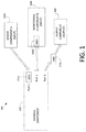
- the system 100 may comprise an avionics component 110 having various ports or interfaces 150 in communication with various input or output (“I/O") devices or other components 102. Although these are shown as distinct physical ports, these could be viewed as logical ports, where information to the various components 102a, 102b, 104 is multiplexed over a single physical communications facility.
- I/O devices may comprise in one embodiment, for illustrations purposes, a sensor component 102a, a monitoring component 102b, and output component 104. The function and purpose of these components can vary and are not limited to the embodiments described herein.
- These components 102a, 102b, and 104 could be input, output, or a combination thereof as appropriate.
- these I/O components, as well as the avionics component can comprise various hardware/software configurations, using single or multiple microprocessors, parallel processors, or other programmable logic circuitry.
- FIG. 1 illustrates the avionics component 110 comprising three ports that are in communication with the three separate components, 102a, 102b, and 104 that use different electrical interfaces.
- one embodiment of the present disclosure allows a single, dynamically reconfigurable component to be replicated and associated with each port for interfacing with each of the distinct electrical interfaces.
- This embodiment illustrates three different approaches for applying the principles of the present disclosure, and illustrates how a single genetic DREI can be used to implement a variety of electrical interfaces.
- Use of a common DREI that can be adapted for a variety of communication interfaces facilitates the design, manufacturing, testing, and repair of the components in FIG. 1 , and can reduce overall costs associated with manufacturing and maintaining complex systems, such as those used in aircraft.
- FIG. 1 also shows the avionics component 110 incorporating a DREI within its physical assembly.
- This allows the desired communications interface and protocol to appear as part of the component 110 to the sensor component 102a.
- the communication is unidirectional, but could be bi-directional.
- any sensor component 102a compatible with the desired communications interface can readily plug into, and communicate with, the avionics component 110.
- the avionics component 110 may incorporate other types of interfaces, adopting the principles of the present disclosure allows the subsystem to readily adapt to communicate with a variety of devices.
- the DREI 150b can be incorporated into a monitoring component 102b itself.
- This embodiment illustrates a monitoring component 102b which could provide data to the avionics component upon request.
- the communication is bidirectional and shown with a bidirectional arrow.
- the monitoring component 102b may be "converted" to use a communications protocol recognized by the component 110 and which is otherwise not native to the component 102b.
- Still another embodiment involves using a separate standalone DREI 150c that is distinct from the avionics component 110 and the output component 104.
- the DREI allows otherwise incompatible components to communicate with each other via the intermediate DREI 150c.
- the DREI in this embodiment may incorporate further functionality in the DREI so as to communicate with the avionic system 110. Further, in any of these configurations, multiple DREIs could be incorporated allowing multiple distinct physical or logical interfaces to be provided.
- FIG. 1 illustrates three applications of a DREI in different configurations.
- only a single DREI may be incorporated, or some other combination that is not shown in FIG. 1 .
- a plurality of DREIs could be incorporated into any of the above configurations.
- the DREI may be involved in converting data from one protocol to another.
- the DREI may incorporate well-known data communication protocols, such as but not limited to, a microcomputer bus (e.g., peripheral component interconnect "PCI" bus).
- PCI peripheral component interconnect
- the DREI 150a could be implemented as a board which is inserted into a computer, and communicates over an internal computer bus.
- the principles herein can be adapted for a variety of purposes, and are not limited to avionics, but can be applied to various other communication applications, which can be incorporated into different components. This can include other systems that typically include a number of interfaces on automobiles, ships, trains, military conveyance vehicles, consumer electronic devices, appliances, building control systems, power control systems, etc.
- FIG. 2 illustrates one embodiment of the DREI 200.
- This embodiment illustrates a bidirectional communication arrangement, where the DREI receives incoming information, and transmits outgoing information.
- the information provided to/from the DREI is in digital form, and for illustration purposes, the term "messages" can be used to describe control information defined in the applicable interface, which can be used to convey commands or data.
- messages can be used to describe control information defined in the applicable interface, which can be used to convey commands or data.
- One skilled in the art can adapt the principles of the present disclosure to apply to receiving and generating analog signals as well as digital messages.
- the DREI 200 receives input signals 241a associated with a specific communications protocol and is able, in one embodiment, to process the same and communicate corresponding or responsive signals over a common bi-directional I/O system interface 201. Similarly, the DREI 200 is able to receive information on the common I/O system interface 201, and generate interface specific communications output signals 241b. In other embodiments, the DREI is able to act on the received signals, or generate output signals on its own accord. This same DREI 200 can be reprogrammed or reconfigured for various types of specific communication protocols used on inputs/output 241 as needed.
- the input signals 241a, 241b can be differential signaling, or in other embodiments, can be single-ended signaling. Further, a plurality of different input signals can be received.
- input signals 241a comprise a transmission of a particular communications protocol that is received by DREI 200. These signals can be conveyed on a two-wire interface, which are received at an input port of switch 250.
- the switch 250 may route the incoming signals over ports 233a to a signaling path conditioning component 240, or the switch 250 can bypass the signal conditioning path unit 240 and route the input signals directly to switch 230.
- the signal conditioning path unit 240 may adapt, modify, or otherwise adjust the signals in a first level of processing so that the input signals have characteristics that are compatible with the subsequent processing components (e.g., switch 230 or amplifier 222) so as to comply with a particular standard.
- MIL-STD-1553B indicates that incoming signals should be routed to isolation transformers, whereas other standards do not specific this.
- switch 250 may be used to route the incoming signal 241a to the proper signal conditioning path unit 240.
- the input signals 241a could be received as optically based signals, whereas the DREI 200 is electrically based.
- the signal conditioning path unit could comprise an optical-to-electrical conversion circuitry.
- step-down transformers can be used to condition the signals to modify the input signal.
- Other components in the signal conditioning path may limit, protect, modify, or protect against dangerous voltage levels occurring at the inputs 241a or alter the current or impedance characteristics.
- Switch 230 serves to route the differential signals 225a, 225b to the respective proper amplifier 222a or 222b. In other embodiments, the switch 230 may not be present, but incorporating this functionality allows additional flexibility as will be seen.
- the switch 230 allows the input or output lines to be dynamically reconfigured and a processor 204 controls the switch 230 (as well as switch 250) using a switch control signal or switch control instructions sent to the switch 230 via control lines 207. For example, if the DREI 200 were to handle two separate inputs 241 a, the switch 230 and switch 250 can assist in accommodating this capability and route the corresponding input signals to two signal conditioning path units.
- the processor 204 could instruct the switch accordingly via control line 207 to accept inputs on 241b.
- the switch is controlled in this embodiment by processor 204 generating a switch control signal, but the switch can be controlled by external inputs in other embodiments.
- control input 202 to the processor 204 could be extended to control the switch 230 and/or 250 directly.
- the resulting conditioned or modified input signals are provided as an input signal to the signal level adjusting unit 220, which comprises in one embodiment operational amplifiers 222a, 222b.
- operation amplifier 222a receives the signal input and generates a further modified signal which is a voltage adjusted signal on output line 213.
- the appropriate adjustment level can be controlled by the processor 204 via an amplifier control signal on control lines 207.
- the control line 207 multiplexes various control to the signal adjusting unit 220 and the switches 230, 250, but separate control lines could be employed as well.
- the amplifier 222a further modifies the signals and ensures that the signal levels provided by the amplifier at output 213 are normalized to the expected levels.
- any input signal 241a is converted to a signal-level electrical signal with an appropriate level that can be read by the analog-to-digital converter ("ADC") 210.
- ADC analog-to-digital converter
- the input signal levels to the ADC 210 are typically no greater than the maximum input level that can be processed by the ADC in order to provide an accurate value. Otherwise, levels that exceed the input of the ADC will be mapped to a single numerical value. This may be acceptable in some embodiments.
- the output 213 of the amplifier is received by the ADC 210.
- the ADC 210 receives an analog signal and converts it to a digital value.
- the ADC 210 converts the voltage signal to a numerical value that is communicated over lines 203 to a processor 204.
- the ADC 210 should be capable of digitizing input sufficiently fast enough so that changing incoming information conveyed for the processor 204 is not lost. This speed is dependent on the nature of the output 213.
- the processor 204 then applies the appropriate communication processing rules to determine the appropriate syntax, semantics, and procedures to ascertain the messages being transmitted over interface 241a.
- the processor 204 can store one or more communication library routines for ascertaining the corresponding signal levels, timing, and encoding schemes used, so that the processor 204 can ascertain what message was sent to the DREI at the input signal 241a, and what protocol procedures are to be applied for interpreting the input signal 241 a on the numerical values received at the processor 204.
- the processor can automatically configure itself based on detecting incoming signals and compare their characteristics against a known characteristics table to determine the interface. The processor can report the interface to another processing entity, or select the appropriate communication library routine to use.
- the processor 204 may convert this information over a common I/O interface 201 which can be formatted to another standard (e.g., a PCI bus).
- Interface 201 may be the backplane or data bus of a known computing architecture, such as, but not limited to, Virtual Memory Extension ("VME"), Micro Channel Architecture (“MCA”), or Peripheral Component Interconnect (“PCI").
- VME Virtual Memory Extension
- MCA Micro Channel Architecture
- PCI Peripheral Component Interconnect
- the processor 204 may incorporate other application level control logic to handle the received message (e.g., the processor may act on the received information). In this case, there may not be any need for the processor 204 to relay the information to another entity.
- the processor 204 may utilize stored program information in memory 214 to determine the application specific information to be sent.
- the memory can be of various forms well known in the art, and can be integrated into the same integrated circuit as the processor, or stored in a separate circuit.
- the memory can be various forms of volatile or non-volatile memory.
- the incoming message on interface 241a is a request for a certain type of data, for example, this request can be routed by the processor via interface 201 to another component in the avionics controller 110. This component will respond to the processor 204 over the interface 201 with the requested data. Depending on the particular interface 241 a, the response may be sent by the processor 304 in a particular manner over output 241b.
- the processor 204 determines the appropriate message, encoding, timing, etc. to be used based on the library of instructions for each electrical interface. It is possible in some embodiments that input signal on interface 241a is a different electrical interface than the output interface 241b.
- the processor 204 generates the appropriate numerical values over lines 205 to the digital-to-analog converter ("DAC" 212) which generates a discrete voltage level signal in response.
- DAC digital-to-analog converter
- This value will be the appropriate value for representing the appropriate signal after processing by the subsequent units. For example, if the processor is to send a digital bit stream of "101" which has certain duration, voltage, and timing, the processor will generate the appropriate values and present them to DAC 212.
- the DAC in turn converts the digital value to a signal with the appropriate analog voltage level (more specifically, to one of various discrete voltage levels which approximates an analog voltage wave).
- the amplifier 222b generates the appropriate amplified voltage signals 225b, which the switch 230 connects via ports 231b to the signal conditioning path unit 240.
- the amplifier 222b again is controlled by the processor via an amplifier control signal 207 such that the output level is appropriate for the communications intertace 241b. For example, if a logical "1" is represented by a 15V signal for a certain time period, the amplifier 222b is configured to amplify the input signal to the 15V signal.
- the processor 204 controls the duration by providing the appropriate output signal to the DAC 212 for the corresponding duration.
- the amplified output voltage of the DAC is provided to the switch 230 to the signal conditioning path unit 240, if necessary.
- the signal conditioning path unit incorporates the appropriate components for generating the appropriate types of signals at the required level. For example, if the output signal is optical in nature, the signal conditioning path units may have electro-optical converters. Other signaling path condition components can ensure the appropriate impedance, current, voltage, etc. is present on the output. In this manner, the processor can generate a variety of signal levels that are defined to convey a particular message in a particular communications protocol over interface 241b.
- signal conditioning may not be required.
- the output of switch 230 on port 231b can bypass the signal conditioning path unit 240 if no signal conditioning path unit is required.
- the output could be routed directly to switch 250.
- a "null" signal conditioning path function can be defined as being performed by the signal conditioning path unit, effectively accomplishing the same result. If the signal conditioning path unit 240 is not bypassed, then the output is provided via port 231 a of switch 230 to the signal conditioning path unit 240.
- the signal conditioning path unit's 240 output can be provided to switch 250 on ports 233a, which provides the output signal 241b.
- the processor 204 can be a general purpose microprocessor, a special purpose programmed microprocessor, an application specific integrated circuit, or other types of system-on-chip ("SOC") processors. Other types of processors are possible as well.
- the ADC(s) and DAC(s) can be integrated with the processor and can be implemented using a digital signal processor or other special purpose device.
- the memory for storing the rules for processing and generating input/output signals can be stored in memory 214 that is integrated with, or external to, the processor 204.
- the processor can be a field programmable gate array, which may also have integrated ADCs and DACs.
- the amplifiers 220 and/or switches 230, 250 can be integrated with the above components. Those skilled in the art will recognize that other implementations are possible.
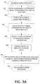
- the operations performed by the device 200 for processing a received input signal on interface 241a are shown in the overview 300 of FIG. 3A . It should be appreciated that more or fewer operations may be performed than shown in the FIG. 3A and described herein. Moreover, these operations may also be performed in a different order than those described herein.
- the input signal received on interface 241a at step 300 is routed in step 301 by switch 250 for conditioning to ensure that the electrical aspects are compatible with the upstream processing components in the device 200. In some other embodiments, the routing of the signal may bypass the signaling conditioning unit.
- the conditioning performed in step 302 may include converting the type of signal or electrical characteristics, such as voltage, current, and impedance.
- the resulting conditioned signal is then provided to another switching element that routes the output to the appropriate amplifier.
- the selected amplifier receives the signal and may amplify the signal to the appropriate signal level, which is still analog in nature, so that it can be processed by the ADC.
- the ADC converts the analog signal to a signal having a digital value (e.g. having one of plurality of discrete values), which in step 310 is processed by the processor to ascertain what information was received. In particular, this processing may involve retrieving information as to the syntax, semantics, and procedures in order to ascertain what messages are being conveyed. At this point the processor has successfully received the input signal, and can recognize the information being conveyed by the corresponding communications protocol.
- the processor's processing of the numerical value presented to the DREI on input port 241a depends on the particular communications interface involved.
- the processor will typically compare the value (which is indicative of a signal level), applicable encoding scheme, timing information, and other aspects to ascertain whether a logical "0" or "1" was sent.
- the processor will apply further rules defining the particular framing structure used for conveying a message in that protocol, and can determine the contents of the message within the framing structure.
- each communications protocol will involve separate and distinct processing by the processor in order to recognize the conveyed syntax and the semantics and can end processing as shown in step 312.
- step 352 the processor provides a numerical digital value that determines the corresponding output signal on interface 241b for the respective electrical interface.
- the numerical value is provided in step 354 to a DAC that converts the numerical value to an analog output.
- step 356 the analog output is provided to an amplifier, which amplifies the signal based on control information provided by the processor.
- step 358 the amplified signal is provided to a switch which routes the amplified signal to the conditioning equipment.
- step 360 the conditioning equipment conditions the signal as appropriate, and provides the output signal at its output interface.
- step 361 another switch receives the output signal and routes it to the appropriate output port.
- the processor has successfully generated an output signal based on the electrical interface specifications for the corresponding communications protocol.
- FIG. 2 is one embodiment capable of processing a single input communications interface 241, comprising both an input 241a and output 241b capability. Other embodiments may employ only an input or an output.
- a plurality of communication interfaces exist, with each interface including an input and output. It may be desirable to communicate with a variety of distinct communications devices on various interfaces using a plurality of communication protocols on the interface 241, either simultaneously, or at different times.
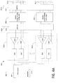
- One such architecture 400 is shown in FIG. 4A . This embodiment illustrates further advantages and flexibility.
- a processor 204 stores in memory 214, or is able to otherwise access, instructions for processing two or more communication protocols, which may be distinct.
- the switch 450, signal conditioning path unit 440a, switch 430, amplifier and ADC/DAC assembly 420a communicates with the processor 204 as described in conjunction with FIG. 2 .
- the ADC/DAC and amplifiers components 420a are replicated n times, as shown by assembly 420n.
- Each assembly 420 is connected to the switch 430 and can be connected to a particular signal conditioning path unit 440n (or bypassed) and then connected to an interface 441a-441n.
- interface 441 a can be, for example, one interface type
- interface 441n can be another interface type. This allows the processor to service two or more different type of interfaces, either simultaneously, or on a time multiplexed basis.
- the ability to handle different signal conditioning path requirements for each interface is also a benefit of the architecture shown in FIG. 4A .
- processor 204 via instructions on interface 402 as to which communications protocol is to be used for interface 441 a and 441n.
- the processor can then apply the appropriate instruction set for processing input/output according to the appropriate protocol.
- the processor can be programmed dynamically to handle different communications protocols for interface 441a and 441n.
- the set of instructions for handling a particular communications protocol can be downloaded to the processor 204 as required.
- a newly developed protocol with different signaling requirements could be accommodated by the system 400 by downloading the appropriate protocol processing instructions to the processor.
- the switch 430 and switch 450 can be instructed via control line 431a and 431b respectively to route the signal to the appropriate amplifier/ADC/DAC assembly 420 and signal conditioning path unit 440.
- a system can be easily reconfigured to handle input (or output) on either of the given interface lines 441a, 441b.
- FIG. 4B shows a portion of the architecture of FIG. 4A and further illustrates one arrangement for connecting the connecting contacts of switch 430 and 450.
- the switches can be analogized in functionality to a relay switch, which either connect to close a circuit, or disconnect to open a circuit.
- interface 441a comprises signals 443a for the input, and signals 443b for the output.
- switch 450 connects the leads 460a, 461b to the lead 460b, 461b. In this manner, the output is provided for the output interface 443b.
- the switches may be an electronic matrix type switching element able to connect any port to any port.
- FIG. 4C the interface 441a again comprises a set of input and output, but the inputs 443 and the outputs 447 are not necessarily arranged as shown in FIG. 4B .
- a set of inputs and outputs could be defined as an interface.
- the switch 450 is able to route signals between port 465b to port 460a, and port 466b to port 461a. This type of arrangement can be used, for example, when a plurality of inputs and outputs for a plurality of interfaces are multiplexed onto a single optical fiber.
- this type of arrangement can provide N+1 redundancy for accommodating a failed signal conditioning path unit. For example, if signal conditioning path unit 440a fails, then switch 430 and 450 could be instructed instead to use another signal conditioning path unit (e.g., 440n).
- another signal conditioning path unit e.g., 440n
- FIG. 5 Another embodiment 500 is illustrated in FIG. 5 .
- the processor 504 is replicated (504a - 504n).
- each processor 504 is shown connected to a respective memory 514, but in other embodiments, all the processors could access a common memory.
- each processor 504a-504n is associated, in turn, with an ADC/DAC/Amplifier assembly 520a-520n and interconnected with a common switch 530.
- the switch in turn, is connected to n number of signal conditional path units 540a-540n as appropriate.
- the outputs of the signal conditioning path unit are provided to another switch 550, which then presents the signal on the interfaces 541a-541n as appropriate.
- each processor 504 is configured to handle a specific interface 541. With this architecture, a unit with n processors and n interfaces could be configured to handle n different communication protocols.
- a single dynamically reconfigurable interface structure (e.g., system 200, 400 or 500) can be readily adapted to handle one or more communication interfaces.
- a single interface structure could have instructions loaded into storage that are used by a processor for handling a particular communication interface ("Protocol A").
- Process B a communication interface
- This could be accomplished by using the same interface structure 200, but reconfiguring the DREI instead with instructions for a different communication interface (Protocol B).
- a single interface structure board could be stocked in a parts depot and configured to replace a variety of units, thus eliminating a need to stock a component for every possible interface type.
- a DREI could be loaded with instructions to handle a variety of communication interfaces after it was installed (as opposed to being loaded with the appropriate instructions before installation).
- other (external) components could configure the processor to select and use a given communication interface. In this manner, an easily reconfigurable replacement module could be defined.
Landscapes
- Engineering & Computer Science (AREA)
- Theoretical Computer Science (AREA)
- General Engineering & Computer Science (AREA)
- Physics & Mathematics (AREA)
- General Physics & Mathematics (AREA)
- Computer Hardware Design (AREA)
- Communication Control (AREA)
- Amplifiers (AREA)
- Information Transfer Systems (AREA)
- Bus Control (AREA)
Applications Claiming Priority (2)
| Application Number | Priority Date | Filing Date | Title |
|---|---|---|---|
| US13/162,260 US8751069B2 (en) | 2011-06-16 | 2011-06-16 | Dynamically reconfigurable electrical interface |
| PCT/US2012/038209 WO2012173732A1 (en) | 2011-06-16 | 2012-05-16 | Dynamically reconfigurable electrical interface |
Publications (2)
| Publication Number | Publication Date |
|---|---|
| EP2721502A1 EP2721502A1 (en) | 2014-04-23 |
| EP2721502B1 true EP2721502B1 (en) | 2016-08-24 |
Family
ID=46246187
Family Applications (1)
| Application Number | Title | Priority Date | Filing Date |
|---|---|---|---|
| EP12726946.2A Active EP2721502B1 (en) | 2011-06-16 | 2012-05-16 | Dynamically reconfigurable electrical interface |
Country Status (6)
| Country | Link |
|---|---|
| US (1) | US8751069B2 (https=) |
| EP (1) | EP2721502B1 (https=) |
| JP (1) | JP6058649B2 (https=) |
| KR (1) | KR101881623B1 (https=) |
| CN (1) | CN103608795B (https=) |
| WO (1) | WO2012173732A1 (https=) |
Families Citing this family (17)
| Publication number | Priority date | Publication date | Assignee | Title |
|---|---|---|---|---|
| US8713404B2 (en) * | 2011-07-01 | 2014-04-29 | Apple Inc. | Controller interface providing improved data reliability |
| US9313773B2 (en) * | 2013-03-14 | 2016-04-12 | The Boeing Company | Aircraft communications switching system |
| FR3005225B1 (fr) * | 2013-04-26 | 2016-10-21 | Snecma | Dispositif de conversion d'un signal arinc en un signal optique, systeme de test anti foudre |
| US9404968B1 (en) * | 2013-10-25 | 2016-08-02 | Altera Corporation | System and methods for debug connectivity discovery |
| JP6241216B2 (ja) * | 2013-11-12 | 2017-12-06 | セイコーエプソン株式会社 | センサーデバイス、センサーユニット及び電子機器 |
| KR101560224B1 (ko) | 2014-10-27 | 2015-10-14 | 현대자동차주식회사 | 센터페시아 통합 인터페이스 제공 방법 및 장치 |
| US20160188525A1 (en) * | 2014-12-30 | 2016-06-30 | Ge Aviation Systems Llc | Apparatus with configurable serial ports |
| US10073806B2 (en) * | 2015-05-13 | 2018-09-11 | Qualcomm Incorporated | Apparatus and methods for providing a reconfigurable bidirectional front-end interface |
| DE102016200964A1 (de) * | 2016-01-25 | 2017-07-27 | Siemens Aktiengesellschaft | Verfahren zur Informationsübertragung in einem Kommunikationsnetz |
| JP2017146721A (ja) * | 2016-02-16 | 2017-08-24 | 日本飛行機株式会社 | 航空機データバスライン連接方法 |
| CN105867190B (zh) * | 2016-04-15 | 2018-11-27 | 北京博瑞云飞科技发展有限公司 | 无人驾驶飞行器的接口系统和接口控制方法 |
| CN105739516A (zh) * | 2016-05-09 | 2016-07-06 | 王彦成 | 无人机管控装置及相应的系统 |
| CN106055509B (zh) * | 2016-05-31 | 2022-08-05 | 珠海格力电器股份有限公司 | 一种光纤通信系统及光纤通信的配置方法 |
| US11411293B1 (en) * | 2021-09-10 | 2022-08-09 | Nanotronics Imaging, Inc. | Fault protected signal splitter apparatus |
| US11894596B2 (en) | 2021-09-10 | 2024-02-06 | Nanotronics Imaging, Inc. | Fault protected signal splitter apparatus |
| WO2023091867A1 (en) * | 2021-11-17 | 2023-05-25 | Battelle Energy Alliance, Llc | Observing signals in a network and/or identifying signaling protocols and related devices, systems, and methods |
| CN115103035A (zh) * | 2022-07-29 | 2022-09-23 | 中国民航大学 | 基于arinc429总线的电气协议转换电路系统 |
Family Cites Families (20)
| Publication number | Priority date | Publication date | Assignee | Title |
|---|---|---|---|---|
| US5036465A (en) * | 1989-10-03 | 1991-07-30 | Grumman Aerospace Corporation | Method of controlling and monitoring a store |
| US5091847A (en) * | 1989-10-03 | 1992-02-25 | Grumman Aerospace Corporation | Fault tolerant interface station |
| JPH06161948A (ja) * | 1992-11-18 | 1994-06-10 | Matsushita Electric Ind Co Ltd | データ転送装置 |
| JPH06231070A (ja) * | 1993-02-03 | 1994-08-19 | Nec Yamagata Ltd | インターフェース装置 |
| US5453744A (en) * | 1993-11-23 | 1995-09-26 | Alliedsignal Inc. | Device for modular input high-speed multi-channel digitizing of electrical data |
| US5923663A (en) * | 1997-03-24 | 1999-07-13 | Compaq Computer Corporation | Method and apparatus for automatically detecting media connected to a network port |
| US6362768B1 (en) * | 1999-08-09 | 2002-03-26 | Honeywell International Inc. | Architecture for an input and output device capable of handling various signal characteristics |
| US6684347B1 (en) | 2000-08-10 | 2004-01-27 | Adc Telecommunications, Inc. | Method and system for MDI crossover control |
| US6615116B2 (en) * | 2001-08-09 | 2003-09-02 | The Boeing Company | Method and apparatus for communicating between an aircraft and an associated store |
| WO2004114492A2 (en) * | 2003-06-13 | 2004-12-29 | Tdg Aerospace, Inc. | Systems and methods for fault-based power signal interruption |
| US7139878B2 (en) * | 2003-06-20 | 2006-11-21 | Freescale Semiconductor, Inc. | Method and apparatus for dynamic prefetch buffer configuration and replacement |
| US7864689B2 (en) * | 2003-07-02 | 2011-01-04 | Broadcom Corp. | Method and system for automatic media dependent interface reconfiguration and repair |
| CN1890913A (zh) * | 2003-12-08 | 2007-01-03 | 硅谷数模半导体有限公司 | 用于长程10和100Mbps以太网传输的信令和编码方法和装置 |
| US6941850B1 (en) * | 2004-01-09 | 2005-09-13 | Raytheon Company | Self-contained airborne smart weapon umbilical control cable |
| US7280810B2 (en) * | 2005-08-03 | 2007-10-09 | Kamilo Feher | Multimode communication system |
| US7852913B2 (en) * | 2005-10-03 | 2010-12-14 | Clariphy Communications, Inc. | High-speed receiver architecture |
| US20100217899A1 (en) * | 2007-01-31 | 2010-08-26 | Raytheon Company | Munitions control unit |
| WO2008107737A1 (en) * | 2007-03-05 | 2008-09-12 | Nokia Corporation | Providing feedback in an electronic circuit |
| JP2009094782A (ja) * | 2007-10-09 | 2009-04-30 | Hitachi Ltd | 半導体システム |
| JP5465965B2 (ja) * | 2009-03-31 | 2014-04-09 | ルネサスエレクトロニクス株式会社 | データ処理装置及びデータ処理システム |
-
2011
- 2011-06-16 US US13/162,260 patent/US8751069B2/en active Active
-
2012
- 2012-05-16 EP EP12726946.2A patent/EP2721502B1/en active Active
- 2012-05-16 CN CN201280029152.3A patent/CN103608795B/zh active Active
- 2012-05-16 JP JP2014515827A patent/JP6058649B2/ja active Active
- 2012-05-16 WO PCT/US2012/038209 patent/WO2012173732A1/en not_active Ceased
- 2012-05-16 KR KR1020137026688A patent/KR101881623B1/ko active Active
Also Published As
| Publication number | Publication date |
|---|---|
| WO2012173732A1 (en) | 2012-12-20 |
| CN103608795B (zh) | 2017-02-15 |
| JP2014527209A (ja) | 2014-10-09 |
| US20120323409A1 (en) | 2012-12-20 |
| KR101881623B1 (ko) | 2018-07-24 |
| EP2721502A1 (en) | 2014-04-23 |
| US8751069B2 (en) | 2014-06-10 |
| JP6058649B2 (ja) | 2017-01-11 |
| KR20140029403A (ko) | 2014-03-10 |
| CN103608795A (zh) | 2014-02-26 |
Similar Documents
| Publication | Publication Date | Title |
|---|---|---|
| EP2721502B1 (en) | Dynamically reconfigurable electrical interface | |
| US7996577B2 (en) | Automatically switching console connection | |
| EP2146286B1 (en) | Converter and control system | |
| US7715433B2 (en) | Universal controller and signal monitor | |
| US20170068628A1 (en) | Reducing ethernet latency in a multi-server chassis | |
| US8155801B2 (en) | Architecture with optimized interfacing for an aircraft hybrid cockpit control panel system | |
| US10663964B2 (en) | Unified and redundant flight and mission control for an unmanned aerial vehicle | |
| EP3049894A1 (en) | Flexible mobile device connectivity to automotive systems with usb hubs | |
| US12413443B2 (en) | USB type-C/PD port real time monitoring and control in an automotive or industrial ecosystem | |
| US20120265919A1 (en) | Interface device and wiring board | |
| US20030033374A1 (en) | Method and system for implementing a communications core on a single programmable device | |
| US8478927B2 (en) | USB hub supporting unequal numbers of high-speed and super-speed ports | |
| CA2845231A1 (en) | Interface system for multiple protocols | |
| US8903569B2 (en) | Method for controlling a high-lift device or a flight control surface, system and aircraft or spacecraft | |
| US20120054392A1 (en) | Data read and write device and method for usb ports of 1-wire devices | |
| EP3620924A1 (en) | Selectable system controller for multi-processor computing systems | |
| US20070160075A1 (en) | Device, system and method of communicating between a bus controller and one or more remote terminals | |
| CN105993008A (zh) | 高频装置及该高频装置的控制方法 | |
| US20160006185A1 (en) | Converter jack | |
| US20100312937A1 (en) | Interface card with extensible input/output interface | |
| US8954623B2 (en) | Universal Serial Bus devices supporting super speed and non-super speed connections for communication with a host device and methods using the same | |
| CN104685427A (zh) | 适合在变电站自动化系统中使用的智能电子设备以及对其进行操作的方法 | |
| Jose | An FPGA implementation of 1553 protocol controller | |
| KR101649824B1 (ko) | Emc 시험 시스템 | |
| CN114859773B (zh) | 一种采样与传输监控电路、模组、通信芯片、车辆及方法 |
Legal Events
| Date | Code | Title | Description |
|---|---|---|---|
| PUAI | Public reference made under article 153(3) epc to a published international application that has entered the european phase |
Free format text: ORIGINAL CODE: 0009012 |
|
| 17P | Request for examination filed |
Effective date: 20140113 |
|
| AK | Designated contracting states |
Kind code of ref document: A1 Designated state(s): AL AT BE BG CH CY CZ DE DK EE ES FI FR GB GR HR HU IE IS IT LI LT LU LV MC MK MT NL NO PL PT RO RS SE SI SK SM TR |
|
| DAX | Request for extension of the european patent (deleted) | ||
| GRAP | Despatch of communication of intention to grant a patent |
Free format text: ORIGINAL CODE: EPIDOSNIGR1 |
|
| INTG | Intention to grant announced |
Effective date: 20160302 |
|
| GRAS | Grant fee paid |
Free format text: ORIGINAL CODE: EPIDOSNIGR3 |
|
| GRAA | (expected) grant |
Free format text: ORIGINAL CODE: 0009210 |
|
| AK | Designated contracting states |
Kind code of ref document: B1 Designated state(s): AL AT BE BG CH CY CZ DE DK EE ES FI FR GB GR HR HU IE IS IT LI LT LU LV MC MK MT NL NO PL PT RO RS SE SI SK SM TR |
|
| REG | Reference to a national code |
Ref country code: GB Ref legal event code: FG4D |
|
| REG | Reference to a national code |
Ref country code: CH Ref legal event code: EP |
|
| REG | Reference to a national code |
Ref country code: AT Ref legal event code: REF Ref document number: 823638 Country of ref document: AT Kind code of ref document: T Effective date: 20160915 |
|
| REG | Reference to a national code |
Ref country code: IE Ref legal event code: FG4D |
|
| REG | Reference to a national code |
Ref country code: DE Ref legal event code: R096 Ref document number: 602012022194 Country of ref document: DE |
|
| REG | Reference to a national code |
Ref country code: LT Ref legal event code: MG4D |
|
| REG | Reference to a national code |
Ref country code: NL Ref legal event code: MP Effective date: 20160824 |
|
| REG | Reference to a national code |
Ref country code: AT Ref legal event code: MK05 Ref document number: 823638 Country of ref document: AT Kind code of ref document: T Effective date: 20160824 |
|
| PG25 | Lapsed in a contracting state [announced via postgrant information from national office to epo] |
Ref country code: IT Free format text: LAPSE BECAUSE OF FAILURE TO SUBMIT A TRANSLATION OF THE DESCRIPTION OR TO PAY THE FEE WITHIN THE PRESCRIBED TIME-LIMIT Effective date: 20160824 Ref country code: HR Free format text: LAPSE BECAUSE OF FAILURE TO SUBMIT A TRANSLATION OF THE DESCRIPTION OR TO PAY THE FEE WITHIN THE PRESCRIBED TIME-LIMIT Effective date: 20160824 Ref country code: RS Free format text: LAPSE BECAUSE OF FAILURE TO SUBMIT A TRANSLATION OF THE DESCRIPTION OR TO PAY THE FEE WITHIN THE PRESCRIBED TIME-LIMIT Effective date: 20160824 Ref country code: FI Free format text: LAPSE BECAUSE OF FAILURE TO SUBMIT A TRANSLATION OF THE DESCRIPTION OR TO PAY THE FEE WITHIN THE PRESCRIBED TIME-LIMIT Effective date: 20160824 Ref country code: LT Free format text: LAPSE BECAUSE OF FAILURE TO SUBMIT A TRANSLATION OF THE DESCRIPTION OR TO PAY THE FEE WITHIN THE PRESCRIBED TIME-LIMIT Effective date: 20160824 Ref country code: NL Free format text: LAPSE BECAUSE OF FAILURE TO SUBMIT A TRANSLATION OF THE DESCRIPTION OR TO PAY THE FEE WITHIN THE PRESCRIBED TIME-LIMIT Effective date: 20160824 Ref country code: NO Free format text: LAPSE BECAUSE OF FAILURE TO SUBMIT A TRANSLATION OF THE DESCRIPTION OR TO PAY THE FEE WITHIN THE PRESCRIBED TIME-LIMIT Effective date: 20161124 |
|
| PG25 | Lapsed in a contracting state [announced via postgrant information from national office to epo] |
Ref country code: PT Free format text: LAPSE BECAUSE OF FAILURE TO SUBMIT A TRANSLATION OF THE DESCRIPTION OR TO PAY THE FEE WITHIN THE PRESCRIBED TIME-LIMIT Effective date: 20161226 Ref country code: ES Free format text: LAPSE BECAUSE OF FAILURE TO SUBMIT A TRANSLATION OF THE DESCRIPTION OR TO PAY THE FEE WITHIN THE PRESCRIBED TIME-LIMIT Effective date: 20160824 Ref country code: GR Free format text: LAPSE BECAUSE OF FAILURE TO SUBMIT A TRANSLATION OF THE DESCRIPTION OR TO PAY THE FEE WITHIN THE PRESCRIBED TIME-LIMIT Effective date: 20161125 Ref country code: SE Free format text: LAPSE BECAUSE OF FAILURE TO SUBMIT A TRANSLATION OF THE DESCRIPTION OR TO PAY THE FEE WITHIN THE PRESCRIBED TIME-LIMIT Effective date: 20160824 Ref country code: AT Free format text: LAPSE BECAUSE OF FAILURE TO SUBMIT A TRANSLATION OF THE DESCRIPTION OR TO PAY THE FEE WITHIN THE PRESCRIBED TIME-LIMIT Effective date: 20160824 Ref country code: LV Free format text: LAPSE BECAUSE OF FAILURE TO SUBMIT A TRANSLATION OF THE DESCRIPTION OR TO PAY THE FEE WITHIN THE PRESCRIBED TIME-LIMIT Effective date: 20160824 |
|
| PG25 | Lapsed in a contracting state [announced via postgrant information from national office to epo] |
Ref country code: RO Free format text: LAPSE BECAUSE OF FAILURE TO SUBMIT A TRANSLATION OF THE DESCRIPTION OR TO PAY THE FEE WITHIN THE PRESCRIBED TIME-LIMIT Effective date: 20160824 Ref country code: EE Free format text: LAPSE BECAUSE OF FAILURE TO SUBMIT A TRANSLATION OF THE DESCRIPTION OR TO PAY THE FEE WITHIN THE PRESCRIBED TIME-LIMIT Effective date: 20160824 |
|
| REG | Reference to a national code |
Ref country code: FR Ref legal event code: PLFP Year of fee payment: 6 |
|
| REG | Reference to a national code |
Ref country code: DE Ref legal event code: R097 Ref document number: 602012022194 Country of ref document: DE |
|
| PG25 | Lapsed in a contracting state [announced via postgrant information from national office to epo] |
Ref country code: PL Free format text: LAPSE BECAUSE OF FAILURE TO SUBMIT A TRANSLATION OF THE DESCRIPTION OR TO PAY THE FEE WITHIN THE PRESCRIBED TIME-LIMIT Effective date: 20160824 Ref country code: BG Free format text: LAPSE BECAUSE OF FAILURE TO SUBMIT A TRANSLATION OF THE DESCRIPTION OR TO PAY THE FEE WITHIN THE PRESCRIBED TIME-LIMIT Effective date: 20161124 Ref country code: SK Free format text: LAPSE BECAUSE OF FAILURE TO SUBMIT A TRANSLATION OF THE DESCRIPTION OR TO PAY THE FEE WITHIN THE PRESCRIBED TIME-LIMIT Effective date: 20160824 Ref country code: BE Free format text: LAPSE BECAUSE OF FAILURE TO SUBMIT A TRANSLATION OF THE DESCRIPTION OR TO PAY THE FEE WITHIN THE PRESCRIBED TIME-LIMIT Effective date: 20160824 Ref country code: SM Free format text: LAPSE BECAUSE OF FAILURE TO SUBMIT A TRANSLATION OF THE DESCRIPTION OR TO PAY THE FEE WITHIN THE PRESCRIBED TIME-LIMIT Effective date: 20160824 Ref country code: DK Free format text: LAPSE BECAUSE OF FAILURE TO SUBMIT A TRANSLATION OF THE DESCRIPTION OR TO PAY THE FEE WITHIN THE PRESCRIBED TIME-LIMIT Effective date: 20160824 Ref country code: CZ Free format text: LAPSE BECAUSE OF FAILURE TO SUBMIT A TRANSLATION OF THE DESCRIPTION OR TO PAY THE FEE WITHIN THE PRESCRIBED TIME-LIMIT Effective date: 20160824 |
|
| PLBE | No opposition filed within time limit |
Free format text: ORIGINAL CODE: 0009261 |
|
| STAA | Information on the status of an ep patent application or granted ep patent |
Free format text: STATUS: NO OPPOSITION FILED WITHIN TIME LIMIT |
|
| 26N | No opposition filed |
Effective date: 20170526 |
|
| PG25 | Lapsed in a contracting state [announced via postgrant information from national office to epo] |
Ref country code: SI Free format text: LAPSE BECAUSE OF FAILURE TO SUBMIT A TRANSLATION OF THE DESCRIPTION OR TO PAY THE FEE WITHIN THE PRESCRIBED TIME-LIMIT Effective date: 20160824 Ref country code: LU Free format text: LAPSE BECAUSE OF NON-PAYMENT OF DUE FEES Effective date: 20170531 |
|
| REG | Reference to a national code |
Ref country code: CH Ref legal event code: PL |
|
| PG25 | Lapsed in a contracting state [announced via postgrant information from national office to epo] |
Ref country code: MC Free format text: LAPSE BECAUSE OF FAILURE TO SUBMIT A TRANSLATION OF THE DESCRIPTION OR TO PAY THE FEE WITHIN THE PRESCRIBED TIME-LIMIT Effective date: 20160824 |
|
| REG | Reference to a national code |
Ref country code: IE Ref legal event code: MM4A |
|
| PG25 | Lapsed in a contracting state [announced via postgrant information from national office to epo] |
Ref country code: CH Free format text: LAPSE BECAUSE OF NON-PAYMENT OF DUE FEES Effective date: 20170531 Ref country code: LI Free format text: LAPSE BECAUSE OF NON-PAYMENT OF DUE FEES Effective date: 20170531 |
|
| PG25 | Lapsed in a contracting state [announced via postgrant information from national office to epo] |
Ref country code: LU Free format text: LAPSE BECAUSE OF NON-PAYMENT OF DUE FEES Effective date: 20170516 |
|
| PG25 | Lapsed in a contracting state [announced via postgrant information from national office to epo] |
Ref country code: IE Free format text: LAPSE BECAUSE OF NON-PAYMENT OF DUE FEES Effective date: 20170516 |
|
| REG | Reference to a national code |
Ref country code: FR Ref legal event code: PLFP Year of fee payment: 7 |
|
| PG25 | Lapsed in a contracting state [announced via postgrant information from national office to epo] |
Ref country code: MT Free format text: LAPSE BECAUSE OF NON-PAYMENT OF DUE FEES Effective date: 20170516 |
|
| PG25 | Lapsed in a contracting state [announced via postgrant information from national office to epo] |
Ref country code: AL Free format text: LAPSE BECAUSE OF FAILURE TO SUBMIT A TRANSLATION OF THE DESCRIPTION OR TO PAY THE FEE WITHIN THE PRESCRIBED TIME-LIMIT Effective date: 20160824 |
|
| PG25 | Lapsed in a contracting state [announced via postgrant information from national office to epo] |
Ref country code: HU Free format text: LAPSE BECAUSE OF FAILURE TO SUBMIT A TRANSLATION OF THE DESCRIPTION OR TO PAY THE FEE WITHIN THE PRESCRIBED TIME-LIMIT; INVALID AB INITIO Effective date: 20120516 |
|
| PG25 | Lapsed in a contracting state [announced via postgrant information from national office to epo] |
Ref country code: CY Free format text: LAPSE BECAUSE OF NON-PAYMENT OF DUE FEES Effective date: 20160824 |
|
| PG25 | Lapsed in a contracting state [announced via postgrant information from national office to epo] |
Ref country code: MK Free format text: LAPSE BECAUSE OF FAILURE TO SUBMIT A TRANSLATION OF THE DESCRIPTION OR TO PAY THE FEE WITHIN THE PRESCRIBED TIME-LIMIT Effective date: 20160824 |
|
| PG25 | Lapsed in a contracting state [announced via postgrant information from national office to epo] |
Ref country code: TR Free format text: LAPSE BECAUSE OF FAILURE TO SUBMIT A TRANSLATION OF THE DESCRIPTION OR TO PAY THE FEE WITHIN THE PRESCRIBED TIME-LIMIT Effective date: 20160824 |
|
| PG25 | Lapsed in a contracting state [announced via postgrant information from national office to epo] |
Ref country code: IS Free format text: LAPSE BECAUSE OF FAILURE TO SUBMIT A TRANSLATION OF THE DESCRIPTION OR TO PAY THE FEE WITHIN THE PRESCRIBED TIME-LIMIT Effective date: 20161224 |
|
| REG | Reference to a national code |
Ref country code: DE Ref legal event code: R082 Ref document number: 602012022194 Country of ref document: DE Representative=s name: KILBURN & STRODE LLP, NL |
|
| P01 | Opt-out of the competence of the unified patent court (upc) registered |
Effective date: 20230516 |
|
| PGFP | Annual fee paid to national office [announced via postgrant information from national office to epo] |
Ref country code: DE Payment date: 20250529 Year of fee payment: 14 |
|
| PGFP | Annual fee paid to national office [announced via postgrant information from national office to epo] |
Ref country code: GB Payment date: 20250527 Year of fee payment: 14 |
|
| PGFP | Annual fee paid to national office [announced via postgrant information from national office to epo] |
Ref country code: FR Payment date: 20250526 Year of fee payment: 14 |