EP2719081B1 - Modifizierte dynamische elementanpassung zur verringerung der latenz bei einem analog-digital-wandler einer pipeline - Google Patents
Modifizierte dynamische elementanpassung zur verringerung der latenz bei einem analog-digital-wandler einer pipeline Download PDFInfo
- Publication number
- EP2719081B1 EP2719081B1 EP12731225.4A EP12731225A EP2719081B1 EP 2719081 B1 EP2719081 B1 EP 2719081B1 EP 12731225 A EP12731225 A EP 12731225A EP 2719081 B1 EP2719081 B1 EP 2719081B1
- Authority
- EP
- European Patent Office
- Prior art keywords
- adc
- circuit
- output
- accordance
- hdc
- Prior art date
- Legal status (The legal status is an assumption and is not a legal conclusion. Google has not performed a legal analysis and makes no representation as to the accuracy of the status listed.)
- Active
Links
Images


Classifications
-
- H—ELECTRICITY
- H03—ELECTRONIC CIRCUITRY
- H03M—CODING; DECODING; CODE CONVERSION IN GENERAL
- H03M1/00—Analogue/digital conversion; Digital/analogue conversion
- H03M1/06—Continuously compensating for, or preventing, undesired influence of physical parameters
-
- H—ELECTRICITY
- H03—ELECTRONIC CIRCUITRY
- H03M—CODING; DECODING; CODE CONVERSION IN GENERAL
- H03M1/00—Analogue/digital conversion; Digital/analogue conversion
- H03M1/06—Continuously compensating for, or preventing, undesired influence of physical parameters
- H03M1/0617—Continuously compensating for, or preventing, undesired influence of physical parameters characterised by the use of methods or means not specific to a particular type of detrimental influence
- H03M1/0634—Continuously compensating for, or preventing, undesired influence of physical parameters characterised by the use of methods or means not specific to a particular type of detrimental influence by averaging out the errors, e.g. using sliding scale
- H03M1/0656—Continuously compensating for, or preventing, undesired influence of physical parameters characterised by the use of methods or means not specific to a particular type of detrimental influence by averaging out the errors, e.g. using sliding scale in the time domain, e.g. using intended jitter as a dither signal
- H03M1/066—Continuously compensating for, or preventing, undesired influence of physical parameters characterised by the use of methods or means not specific to a particular type of detrimental influence by averaging out the errors, e.g. using sliding scale in the time domain, e.g. using intended jitter as a dither signal by continuously permuting the elements used, i.e. dynamic element matching
- H03M1/0673—Continuously compensating for, or preventing, undesired influence of physical parameters characterised by the use of methods or means not specific to a particular type of detrimental influence by averaging out the errors, e.g. using sliding scale in the time domain, e.g. using intended jitter as a dither signal by continuously permuting the elements used, i.e. dynamic element matching using random selection of the elements
-
- H—ELECTRICITY
- H03—ELECTRONIC CIRCUITRY
- H03M—CODING; DECODING; CODE CONVERSION IN GENERAL
- H03M1/00—Analogue/digital conversion; Digital/analogue conversion
- H03M1/06—Continuously compensating for, or preventing, undesired influence of physical parameters
- H03M1/0617—Continuously compensating for, or preventing, undesired influence of physical parameters characterised by the use of methods or means not specific to a particular type of detrimental influence
- H03M1/0634—Continuously compensating for, or preventing, undesired influence of physical parameters characterised by the use of methods or means not specific to a particular type of detrimental influence by averaging out the errors, e.g. using sliding scale
- H03M1/0636—Continuously compensating for, or preventing, undesired influence of physical parameters characterised by the use of methods or means not specific to a particular type of detrimental influence by averaging out the errors, e.g. using sliding scale in the amplitude domain
- H03M1/0639—Continuously compensating for, or preventing, undesired influence of physical parameters characterised by the use of methods or means not specific to a particular type of detrimental influence by averaging out the errors, e.g. using sliding scale in the amplitude domain using dither, e.g. using triangular or sawtooth waveforms
- H03M1/0641—Continuously compensating for, or preventing, undesired influence of physical parameters characterised by the use of methods or means not specific to a particular type of detrimental influence by averaging out the errors, e.g. using sliding scale in the amplitude domain using dither, e.g. using triangular or sawtooth waveforms the dither being a random signal
-
- H—ELECTRICITY
- H03—ELECTRONIC CIRCUITRY
- H03M—CODING; DECODING; CODE CONVERSION IN GENERAL
- H03M1/00—Analogue/digital conversion; Digital/analogue conversion
- H03M1/12—Analogue/digital converters
- H03M1/14—Conversion in steps with each step involving the same or a different conversion means and delivering more than one bit
- H03M1/16—Conversion in steps with each step involving the same or a different conversion means and delivering more than one bit with scale factor modification, i.e. by changing the amplification between the steps
- H03M1/164—Conversion in steps with each step involving the same or a different conversion means and delivering more than one bit with scale factor modification, i.e. by changing the amplification between the steps the steps being performed sequentially in series-connected stages
Definitions
- This invention relates generally to analog-to-digital converters. More specifically, this application relates to reduced latency in an analog-to-digital converter.
- the disclosure is associated with high-speed pipeline analog-to-digital converters (ADC's), and may also be extended to other applications and ADC architectures.
- ADC's pipeline analog-to-digital converters
- the techniques described herein may be applied to algorithmic ADCs, also known as cyclic ADCs, to delta-sigma ADCs, to SAR ADCs, etc., and generally to any ADC that may require one or more digital-to-analog converters.
- Pipeline analog-to-digital converters are sub-ranging data converters in which a signal is quantized coarsely in several steps and the results of the different steps are then combined to achieve a high level of quantization accuracy.
- Pipeline ADCs are popular because they may operate at very high speeds (hundreds of MHz, depending on the technology employed) while achieving relatively large dynamic range.
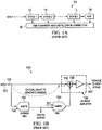
- a typical pipeline ADC 10 includes a plurality of stages 12, 14, ..., L.
- the input Vin is converted using a flash ADC (not shown) and is combined with results from the subsequent stages 14, 16,..., L to form an output.
- the error in each stage is determined by converting the output of that stage using a digital-to-analog converter.
- the difference between the input to the stage and the error is the "residue.”
- the residue for each stage is amplified and fed to the next stage and converted in the same fashion in the next stage.
- the output of the last stage L is provided to a backend ADC 16 which resolves the last bits. All outputs may be provided for time alignment and digital error correction 20.
- a typical stage 100 in a pipeline ADC includes an input signal sampling network 108, an N-bit coarse ADC 102 with its own sampling network, an N-bit digital-to-analog converter 104 (DAC) and an amplifier 106.
- the sampling network 108 and flash ADC 102 sample the input signal 101 at the same time.
- the DAC 104 converts the quantized signal back into analog form and this signal is subtracted 110 from the main input signal 101.
- the residue 105 resulting from this operation is amplified using amplifier 106 in order to occupy, typically and in the absence of errors, a portion of the range of the following stage, for example, half. Ideally, the residue then consists only of quantization noise.
- FIG. 2 illustrates pipeline stage using a prior technique for addressing DAC 104 errors.
- the stage 200 includes an input signal sampling network 208, an N-bit coarse ADC 202 with its own sampling network, an M-bit digital-to-analog converter 204 (DAC) (where M>N) and an amplifier 206.
- Processing elements 232, 234 are added between the coarse ADC 202 and the DAC 204 and hence increase the delay in that path. This delay is critical in high speed operation, namely operation at rates of 250 MSPS and higher.
- An application of the technique of FIG. 2 has been proposed by others to address the problem of element mismatches in flash ADCs, by permuting reference thresholds presented to the comparators to improve the linearity of an ADC.
- DAC and amplifier errors as described above are sometimes estimated and canceled or corrected using Dynamic Element Matching (DEM) and Harmonic Distortion Correction (HDC) techniques.
- DEM Dynamic Element Matching
- HDC Harmonic Distortion Correction
- the pipeline stage includes a DEM block 232 between the coarse ADC 202 and the DAC 204 and the proper placement relative to the stage digital outputs.
- the DEM block 232 can be implemented efficiently through the use of transmission gates. However, it introduces a finite delay which is non-negligible at high clock rates.
- DEM DAC noise cancellation
- a signal ⁇ t is added 234 to the output of the coarse ADC 202.
- This signal consists of the sum of several random, independent sequences that are used in the estimation of the amplifier 206 errors, for example, gain and nonlinearity.
- the number of sequences depends on the order of nonlinearity that needs to be estimated: one sequence for linear gain error, three sequences for harmonic error, and so on.
- backend ADC 212 whose output is provided to amplifier 220 and HDC module 222, whose output is summed 230 with the output of DNC module 226.
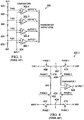
- Four comparators 302.n compare the input voltage on line 304 to four threshold voltages (THR1, THR2, THR3, THR4) respectively. In some implementations, the threshold voltages may be associated with a resistor ladder 306. Other voltage divider techniques may be used as well. If the input voltage is greater than THR1, then comparator 302.1 outputs a logical 1, otherwise it outputs a logical zero. Similarly, comparator 302.2 compares the input voltage with THR2 and so on.
- the output of the coarse ADC 206 is a digital word formed from the outputs of all the comparators. This word is often denominated a "thermometer code.” The number of logical ones contained in the thermometer code is the digital representation of the analog input voltage on line 304.
- the circuit 302.1 includes eight switches 408, 410, 412, 414, 416, 418, 420, 422, two capacitors 402, 404, and a comparator 406.
- the switches are driven by periodic clocks denoted phase 1, phase 2.
- phase 1 is true
- phase 2 is false and vice versa.
- phase 1 is true
- the upper capacitor 402 is charged to the voltage THR1
- the lower capacitor 404 is charged to the input voltage.
- the capacitors are connected to comparator 406.
- the signal output 406 is a logical 1 if the input voltage is greater than the threshold voltage THR1, a logical zero otherwise.
- a prior art pipeline ADC with digital harmonic distortion correction is known from "A 130 mW 100 MS/s Pipelined ADC With 69 dB SNDR Enabled by Digital Harmonic Distortion Correction", by PANIGADA A ET AL, in IEEE JOURNAL OF SOLID-STATE CIRCUITS, vol. 44, no. 12, 1 December 2009, pages 3314-3328 .
- a pipeline ADC is provided in which these problems are overcome in that a DEM function and summation of sequences occur within a flash ADC 202.
- embedding the processing functions needed for DAC and amplifier error correction with the circuitry of a coarse ADC and rearranging the digital calibration blocks HDC and DNC ensures accurate estimation of the errors.
- a circuit in an analog-to-digital converter includes an amplifier configured to receive an output of a backend DAC; a harmonic distortion correction circuit (HDC) coupled to the amplifier and configured to correct distortion components due to the residue amplifier present in a digital signal from the backend ADC, the HDC circuit providing an output to an adder, the adder receiving a coarse digital output from a coarse ADC; and a DAC noise cancellation circuit (DNC) configured to provide an output to the adder, wherein the DNC circuit is configured to correct distortion components due to the DAC present in the digital signal from the backend ADC; wherein the output of the adder is an ADC digital output and wherein the ADC digital output forms an input to the HDC and the DNC.
- HDC harmonic distortion correction circuit
- DNC DAC noise cancellation circuit
- a circuit in a pipeline analog-to-digital converter includes a harmonic distortion correction (HDC) circuit configured to provide an output to an adder, the adder receiving as an input an output of a coarse ADC; and a feedback loop including a DAC noise cancellation (DNC) circuit configured to provide an output to the adder; wherein an output of the adder is an ADC digital output and is an input to the DNC circuit.
- HDC harmonic distortion correction
- DNC DAC noise cancellation
- a method in a pipeline analog-to-digital converter (ADC) for converting an input signal includes performing a harmonic distortion correction as an output to an adder, the adder receiving as another input an output of the coarse ADC; and implementing a feedback loop including a DAC noise cancellation (DNC) circuit providing an output to the adder; wherein an output of the adder is an ADC digital output and is an input to the DNC circuit.
- ADC pipeline analog-to-digital converter
- a pipeline ADC embeds the processing functions needed for the DAC and amplifier error correction with the circuitry of a coarse ADC and also provides a new configuration for digital calibration blocks HDC and DNC, thus ensuring accurate estimation of the errors.
- the calibration of the signal that is the correction portion of the DNC and HDC techniques, may be applied as disclosed in Galton, US Patent No. 6,734,818 and Galton et al., in US Patent No. 7,602,323 , which are incorporated by reference as if fully set forth herein. Other DNC and HDC techniques may be used.
- the estimation of the signal is in accordance with the present disclosure.
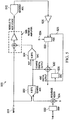
- FIG. 5 illustrates a pipeline stage in accordance with embodiments as claimed.
- the stage 500 includes an N-bit coarse ADC 502, an N-bit digital-to-analog converter 504 (DAC) and an amplifier 506.
- An input 501 is provided to the coarse ADC 502 and the residue amplifier 506.
- Residue of the second-to-last stage may be provided to the backend ADC 512, which is amplified 520 and provided to HDC 522.
- a DEM block 532 and sequences adder 524 are provided at the front end of the coarse ADC 502. This configuration may minimize the propagation time of the critical signal path from the coarse ADC 502 through the DAC 504 to the residue amplifier 506.
- the digital calibration block HDC 522 may receive the sequences ⁇ t, as well as a feedback of the corrected digital output 523.
- the HDC 522 may provide its output to be summed 530 with the output of DNC 526.
- the signal used to estimate the DAC error and the residue amplifier gain error is the ADC digital output 523. Therefore, over time, the estimator will extract and estimate of the residual error after the calibration has been applied. Such estimate may be added to the previous estimates, that is, integrated over time, to improve the accuracy of the calibration. The estimation will converge to the right values once the estimate of the residual error is zero.
- FIG. 6 shows an example 600 of an aspect of the present disclosure of a coarse ADC with DEM 532 and sequences adder 524.
- the threshold voltages THRI, THR2, THR3 and THR4 can be permuted such that each threshold may be connected to any one of the comparators 602.n.
- the signal ⁇ t (random sequences with the properties described above) on line 604 are subtracted from each threshold voltage.
- Each comparator 602.n will compare its input to the difference between one of the thresholds and the signal ⁇ t on line 604.
- FIG. 7 shows an example circuit that realizes the function just described.
- the circuit includes DEM controlled switches 708.1, 708.2, 708.3, and 708.4; HDC controlled switches 706.1, 706.2, 706.3, and 706.4, capacitors 702, 704, comparator 710, phase 1 switches 712a, 712b; and phase 2 switches 714a, 714b, 714c, 714d.
- a DEM and HDC calibration operation will dictate which of the switches is ON at each clock phase cycle.
- the way DEM controls such switches has been described in detail in the disclosures by Galton in U.S. patent 6,734,818 and the way HDC generates the signal ⁇ t has been described in detail in the disclosure by Galton et al in U.S. 7,602,323 .
- the lower capacitor 704 operates as the capacitor 404 in the example of FIG. 4 .
Landscapes
- Engineering & Computer Science (AREA)
- Theoretical Computer Science (AREA)
- Analogue/Digital Conversion (AREA)
Claims (13)
- Schaltung in einem Analog-Digital-Wandler (ADC), die aufweist:einen Grob-ADC (502; 600), der ein Eingangssignal (501) empfängt, das mit einem Digital-Analog-Wandler (DAC) (504) gekoppelt ist, der ein Ausgangssignal erzeugt, das von dem Eingangssignal (501) subtrahiert wird und in einen Restverstärker (506) eingespeist wird, wobei der Grob-ADC (502; 600) und der DAC (504) die gleiche Umwandlungsbitbreite n aufweisen, wobei n eine Ganzzahl ist;einen Verstärker (520), der konfiguriert ist, eine Ausgabe eines mit dem Restverstärker (506) gekoppelten Backend-ADC (512) zu empfangen;einen Harmonic Distortion Correction Circuit (522) (HDC), gekoppelt mit dem Verstärker (520) und konfiguriert, um Verzerrungskomponenten zu korrigieren, die auf Grund des Restverstärkers in einem digitalen Signal des Backend-ADC (512) vorhanden sind, wobei ein HDC Ausgang mit einem ersten Eingang eines Addierers (530) gekoppelt ist, ein zweiter Eingang des Addierers (530) mit einem Ausgang des Grob-ADC (502; 600) gekoppelt ist, wobei die HDC Schaltung (522) konfiguriert ist, eine oder mehrere randomisierte Spannungssequenzen (604) zur Schätzung von Verstärkerfehlern zu empfangen; undeine DAC Störsignalunterdrückungsschaltung (526) (DNC), die einen Ausgang aufweist, der mit einem dritten Eingang des Addierers (530) gekoppelt ist, wobei die DNC Schaltung (526) konfiguriert ist, auf den DAC (504) zurückzuführende Verzerrungskomponenten die in dem digitalen Signal des Backend-ADC (512) vorliegen zu korrigieren;wobei der Ausgang des Addierers (530) ein ADC Digitalausgang ist und wobei der ADC Digitalausgang einen Eingang zu dem HDC (523) und der DNC (526) ausbildet,wobei der Grob-ADC (502; 600) ein Flash-ADC ist, der eine Dynamic Element Matching (DEM) Einheit (532) zur Bereitstellung von Schwellenspannungen (THR) und eine Sequenzaddiereinheit (524) aufweist, die die Schwellenspannungen empfängt, und die eine oder die mehreren randomisierten Spannungssequenzen (604) zur Variation der Schwellenspannungen des Grob-ADC (502; 600).
- Schaltung gemäß Anspruch 1, wobei der Grob-ADC (502; 600) einen Thermometerausgangscode erzeugt, der durch eine Vielzahl von Komparatoren (602) erzeugt wurde, und wobei die Dynamic Element Matching (DEM) Einheit (532) betreibbar ist, die Schwellenspannungen derart zu permutieren, dass jede Schwellenspannung jedem der Komparatoren (602) zugeführt werden kann.
- Schaltung gemäß Anspruch 2, wobei der Grob-ADC (502; 600) weiterhin eine Vielzahl von Sequenzaddierern (524) aufweist, die die Vielzahl von Schwellenspannungen von der DEM Einheit (532) und die eine oder die mehreren randomisierten Sequenzen (604) empfangen.
- Schaltung gemäß einem der vorherigen Ansprüche, wobei die HDC Schaltung (522) konfiguriert ist, einen oder mehrere Steuerausgänge an die DEM Einheit (532) bereitzustellen.
- Schaltung gemäß Anspruch 4, wobei der Grob-ADC (502; 600) für jeden Komparator (602; 710) einen ersten Kondensator (704) und einen zweiten Kondensator (702) und ein Schaltnetzwerk (712, 714) zur Kopplung der Kondensatoren (702, 704) mit dem zugehörigen Komparator (710) aufweist.
- Schaltung gemäß Anspruch 5, wobei der Grob-ADC (502; 600) für jeden Komparator (602; 710) einen ersten Satz von gesteuerten Schaltern (708) aufweist, die durch die DEM Einheit (532) zur Kopplung einer der Schwellenspannungen mit einem Anschluss des zweiten Kondensators (702) gesteuert werden und einen zweiten Satz von gesteuerten Schaltern (706), die durch die HDC Schaltung (522) zur Erzeugung der randomisierten Spannungssequenz und Zuführen von dieser zu dem anderen Anschluss des zweiten Kondensators (702) gesteuert werden.
- Schaltung gemäß Anspruch 5 oder 6, wobei das Schaltnetzwerk (712, 714) durch erste und zweite Phasensteuersignale gesteuert wird.
- Schaltung gemäß einem der vorherigen Ansprüche, wobei die randomisierte Spannungssequenz (604) eine Vielzahl von symmetrischen vorgegebenen Spannungen (VHDC1, VHDC2, VHDC3, VHDC4) umfasst.
- Schaltung gemäß einem der vorherigen Ansprüche 2 bis 8, wobei jeder Komparator (602; 710) gemäß nachfolgender Gleichung arbeitet

- Verfahren zum Betreiben eines Analog-Digital-Wandlers (ADC) gemäß einem der vorherigen Ansprüche, das aufweist:Durchführen einer Harmonic Distortion Correction (HDC) als eine Ausgabe an den Addierer (530);undImplementieren einer Rückkopplungsschleife die umfasst, dass die DAC Störsignalunterdrückung (DNC) Schaltung eine Ausgabe an den Addierer (530) bereitstellt;wobei der Grob-ADC (502; 600) durch Permutieren von Schwellenspannungen des Grob-ADC betrieben wird, die Komparatoren (602) des Flash-ADC (502; 600) zugehörig sind.
- Verfahren gemäß Anspruch 10, wobei unter Steuerung der DEM Einheit (532) jede Schwellenspannung einem Komparator zugewiesen wird und zu jedem Schwellenwert ein Wert der randomisierten Spannungssequenz addiert wird.
- Verfahren gemäß Anspruch 11, wobei während einer ersten Phase ein erster Kondensator (704) mit dem Eingangssignal geladen wird und ein zweiter Kondensator (702) mit einer ausgewählten Schwellenspannung minus einem Wert der randomisierten Spannungssequenz geladen wird.
- Verfahren gemäß Anspruch 12, wobei während einer zweiten Phase die geladenen Kondensatoren (702, 704) mit Eingängen eines zugehörigen Komparators (710) gekoppelt werden.
Applications Claiming Priority (3)
| Application Number | Priority Date | Filing Date | Title |
|---|---|---|---|
| US201161495369P | 2011-06-09 | 2011-06-09 | |
| US13/489,865 US8791844B2 (en) | 2011-06-09 | 2012-06-06 | Modified dynamic element matching for reduced latency in a pipeline analog to digital converter |
| PCT/US2012/041269 WO2012170642A1 (en) | 2011-06-09 | 2012-06-07 | Modified dynamic element matching for reduced latency in a pipeline analog to digital converter |
Publications (2)
| Publication Number | Publication Date |
|---|---|
| EP2719081A1 EP2719081A1 (de) | 2014-04-16 |
| EP2719081B1 true EP2719081B1 (de) | 2017-08-09 |
Family
ID=46420526
Family Applications (1)
| Application Number | Title | Priority Date | Filing Date |
|---|---|---|---|
| EP12731225.4A Active EP2719081B1 (de) | 2011-06-09 | 2012-06-07 | Modifizierte dynamische elementanpassung zur verringerung der latenz bei einem analog-digital-wandler einer pipeline |
Country Status (5)
| Country | Link |
|---|---|
| US (1) | US8791844B2 (de) |
| EP (1) | EP2719081B1 (de) |
| KR (1) | KR101933575B1 (de) |
| CN (1) | CN103703687B (de) |
| WO (1) | WO2012170642A1 (de) |
Families Citing this family (13)
| Publication number | Priority date | Publication date | Assignee | Title |
|---|---|---|---|---|
| US8836558B1 (en) * | 2013-03-15 | 2014-09-16 | Analog Devices, Inc. | Method and device for improving convergence time in correlation-based algorithms |
| US9136856B1 (en) * | 2014-02-26 | 2015-09-15 | Texas Instruments Incorporated | Background DAC calibration for pipeline ADC |
| US9281831B2 (en) * | 2014-03-07 | 2016-03-08 | Integrated Device Technology, Inc. | Digital extraction and correction of the linearity of a residue amplifier in a pipeline ADC |
| CN106100638B (zh) * | 2016-06-14 | 2019-09-03 | 中国电子科技集团公司第二十四研究所 | 流水线模数转换器的误差补偿校正装置 |
| KR102597604B1 (ko) * | 2016-10-19 | 2023-11-10 | 삼성전자주식회사 | 아날로그-디지털 변환기 및 이를 포함하는 이미지 센서 |
| US9906237B1 (en) * | 2017-04-28 | 2018-02-27 | Texas Instruments Incorporated | Digital-to-analog converter and method of operating |
| US10103753B1 (en) | 2017-06-29 | 2018-10-16 | Texas Instruments Incorporated | Error correcting analog-to-digital converters |
| CN109995367B (zh) * | 2017-12-29 | 2022-12-06 | 瑞昱半导体股份有限公司 | 数模转换器装置 |
| CN110336561B (zh) * | 2019-07-05 | 2021-02-05 | 中国电子科技集团公司第二十四研究所 | 一种流水线型模数转换器及其输出校正方法 |
| US10812097B1 (en) * | 2019-09-05 | 2020-10-20 | Semiconductor Components Industries, Llc | Multi-stage analog to digital converter |
| CN111682877B (zh) * | 2020-05-29 | 2023-04-28 | 成都华微电子科技股份有限公司 | 流水线模数转换器的模数转换方法、流水线模数转换器 |
| TWI763498B (zh) * | 2021-05-24 | 2022-05-01 | 瑞昱半導體股份有限公司 | 管線式類比數位轉換器與訊號轉換方法 |
| TWI835424B (zh) * | 2022-11-24 | 2024-03-11 | 瑞昱半導體股份有限公司 | 管線式類比數位轉換器及其校正方法 |
Family Cites Families (18)
| Publication number | Priority date | Publication date | Assignee | Title |
|---|---|---|---|---|
| US6456223B1 (en) * | 1999-12-28 | 2002-09-24 | Texas Instruments Incorporated | Pipelined analog to digital converter using digital mismatch noise cancellation |
| US6396429B2 (en) * | 2000-01-07 | 2002-05-28 | Analog Devices, Inc. | Front-end sampling for analog-to-digital conversion |
| US6734818B2 (en) | 2000-02-22 | 2004-05-11 | The Regents Of The University Of California | Digital cancellation of D/A converter noise in pipelined A/D converters |
| CN1499730A (zh) * | 2002-11-08 | 2004-05-26 | 尹登庆 | 流水线结构的高速高精度模数转换器 |
| DE60310026D1 (de) * | 2003-01-24 | 2007-01-11 | St Microelectronics Srl | Pipeline Analog-Digital-Wandler mit Korrektion von Verstärkungsfehlern zwischen den Stufen |
| EP1441444B1 (de) * | 2003-01-24 | 2007-03-28 | STMicroelectronics S.r.l. | Verfahren zur Korrektion des durch einen Multibit-DA-Wandlers in einem AD-Wandler verursachten Fehlers |
| US7002504B2 (en) * | 2003-05-05 | 2006-02-21 | Maxim Integrated Products, Inc. | Dynamic element matching in high speed data converters |
| US6882292B1 (en) * | 2004-01-07 | 2005-04-19 | Analog Devices, Inc. | Analog to digital converter with bandwidth tuning circuit |
| US7221299B2 (en) * | 2004-06-12 | 2007-05-22 | Nordic Semiconductor Asa | Method and apparatus for an ADC circuit with wider input signal swing |
| US6970120B1 (en) * | 2004-06-12 | 2005-11-29 | Nordic Semiconductor Asa | Method and apparatus for start-up of analog-to-digital converters |
| US7298305B2 (en) * | 2006-03-24 | 2007-11-20 | Cirrus Logic, Inc. | Delta sigma modulator analog-to-digital converters with quantizer output prediction and comparator reduction |
| CN200997595Y (zh) * | 2006-12-07 | 2007-12-26 | 深圳艾科创新微电子有限公司 | 新型模数转换器结构 |
| US7602323B2 (en) | 2007-04-04 | 2009-10-13 | The Regents Of The University Of California | Digital background correction of nonlinear error ADC's |
| US7940198B1 (en) * | 2008-04-30 | 2011-05-10 | V Corp Technologies, Inc. | Amplifier linearizer |
| US7592938B2 (en) * | 2007-07-23 | 2009-09-22 | Mediatek Inc. | Analog-to-digital converter and method of gain error calibration thereof |
| US8106805B2 (en) | 2009-03-05 | 2012-01-31 | Realtek Semiconductor Corp. | Self-calibrating pipeline ADC and method thereof |
| JP2011050028A (ja) | 2009-07-28 | 2011-03-10 | Yokogawa Electric Corp | パイプラインad変換装置 |
| CN102006071B (zh) * | 2010-12-24 | 2012-08-01 | 复旦大学 | 用于流水线结构模数转换器的余量增益电路 |
-
2012
- 2012-06-06 US US13/489,865 patent/US8791844B2/en active Active
- 2012-06-07 EP EP12731225.4A patent/EP2719081B1/de active Active
- 2012-06-07 KR KR1020137034809A patent/KR101933575B1/ko active Active
- 2012-06-07 CN CN201280036965.5A patent/CN103703687B/zh active Active
- 2012-06-07 WO PCT/US2012/041269 patent/WO2012170642A1/en not_active Ceased
Also Published As
| Publication number | Publication date |
|---|---|
| KR101933575B1 (ko) | 2018-12-28 |
| US20130027231A1 (en) | 2013-01-31 |
| US8791844B2 (en) | 2014-07-29 |
| CN103703687B (zh) | 2017-05-03 |
| KR20140035457A (ko) | 2014-03-21 |
| CN103703687A (zh) | 2014-04-02 |
| EP2719081A1 (de) | 2014-04-16 |
| WO2012170642A1 (en) | 2012-12-13 |
Similar Documents
| Publication | Publication Date | Title |
|---|---|---|
| EP2719081B1 (de) | Modifizierte dynamische elementanpassung zur verringerung der latenz bei einem analog-digital-wandler einer pipeline | |
| EP2719082B1 (de) | Modifizierte dynamische elementanpassung zur verringerung der latenz bei einem analog-digital-wandler einer pipeline | |
| US6784814B1 (en) | Correction for pipelined analog to digital (A/D) converter | |
| CN106888018B (zh) | Dac时序失配误差的数字测量 | |
| CN106888020B (zh) | Dac开关失配误差的数字测量 | |
| KR101140349B1 (ko) | 다단 연속 근사 레지스터 아날로그 디지털 변환기 | |
| US7006028B2 (en) | Digital background cancellation of digital to analog converter mismatch noise in analog to digital converters | |
| US8269657B2 (en) | Background calibration of offsets in interleaved analog to digital converters | |
| US6963300B1 (en) | Pipeline analog-to-digital converter | |
| KR20150027582A (ko) | 연속 접근 방식 아날로그-디지털 변환기 및 아날로그-디지털 변환 방법 | |
| JP4543209B2 (ja) | デジタルディザを用いる多段変換器 | |
| US8508392B2 (en) | Pipelined analog digital converter | |
| EP1401105B1 (de) | Offsetspannungskompensationsverfahren für parallele zeitverschachtelte Analog-Digitalwandler sowie Schaltung dafür | |
| US8487792B2 (en) | Method of gain calibration of an ADC stage and an ADC stage | |
| US7728751B2 (en) | Pipelined converter | |
| US10693485B1 (en) | Adaptive background ADC calibration | |
| KR20110090669A (ko) | 축차근사 레지스터형 아날로그-디지털 변환기 |
Legal Events
| Date | Code | Title | Description |
|---|---|---|---|
| PUAI | Public reference made under article 153(3) epc to a published international application that has entered the european phase |
Free format text: ORIGINAL CODE: 0009012 |
|
| 17P | Request for examination filed |
Effective date: 20140108 |
|
| AK | Designated contracting states |
Kind code of ref document: A1 Designated state(s): AL AT BE BG CH CY CZ DE DK EE ES FI FR GB GR HR HU IE IS IT LI LT LU LV MC MK MT NL NO PL PT RO RS SE SI SK SM TR |
|
| DAX | Request for extension of the european patent (deleted) | ||
| GRAP | Despatch of communication of intention to grant a patent |
Free format text: ORIGINAL CODE: EPIDOSNIGR1 |
|
| STAA | Information on the status of an ep patent application or granted ep patent |
Free format text: STATUS: GRANT OF PATENT IS INTENDED |
|
| RIC1 | Information provided on ipc code assigned before grant |
Ipc: H03M 1/16 20060101ALI20161223BHEP Ipc: H03M 1/06 20060101AFI20161223BHEP |
|
| INTG | Intention to grant announced |
Effective date: 20170125 |
|
| GRAS | Grant fee paid |
Free format text: ORIGINAL CODE: EPIDOSNIGR3 |
|
| GRAA | (expected) grant |
Free format text: ORIGINAL CODE: 0009210 |
|
| STAA | Information on the status of an ep patent application or granted ep patent |
Free format text: STATUS: THE PATENT HAS BEEN GRANTED |
|
| AK | Designated contracting states |
Kind code of ref document: B1 Designated state(s): AL AT BE BG CH CY CZ DE DK EE ES FI FR GB GR HR HU IE IS IT LI LT LU LV MC MK MT NL NO PL PT RO RS SE SI SK SM TR |
|
| REG | Reference to a national code |
Ref country code: GB Ref legal event code: FG4D |
|
| REG | Reference to a national code |
Ref country code: CH Ref legal event code: EP Ref country code: AT Ref legal event code: REF Ref document number: 917849 Country of ref document: AT Kind code of ref document: T Effective date: 20170815 |
|
| REG | Reference to a national code |
Ref country code: IE Ref legal event code: FG4D |
|
| REG | Reference to a national code |
Ref country code: DE Ref legal event code: R096 Ref document number: 602012035638 Country of ref document: DE |
|
| REG | Reference to a national code |
Ref country code: NL Ref legal event code: MP Effective date: 20170809 |
|
| REG | Reference to a national code |
Ref country code: LT Ref legal event code: MG4D |
|
| REG | Reference to a national code |
Ref country code: AT Ref legal event code: MK05 Ref document number: 917849 Country of ref document: AT Kind code of ref document: T Effective date: 20170809 |
|
| PG25 | Lapsed in a contracting state [announced via postgrant information from national office to epo] |
Ref country code: LT Free format text: LAPSE BECAUSE OF FAILURE TO SUBMIT A TRANSLATION OF THE DESCRIPTION OR TO PAY THE FEE WITHIN THE PRESCRIBED TIME-LIMIT Effective date: 20170809 Ref country code: NL Free format text: LAPSE BECAUSE OF FAILURE TO SUBMIT A TRANSLATION OF THE DESCRIPTION OR TO PAY THE FEE WITHIN THE PRESCRIBED TIME-LIMIT Effective date: 20170809 Ref country code: SE Free format text: LAPSE BECAUSE OF FAILURE TO SUBMIT A TRANSLATION OF THE DESCRIPTION OR TO PAY THE FEE WITHIN THE PRESCRIBED TIME-LIMIT Effective date: 20170809 Ref country code: NO Free format text: LAPSE BECAUSE OF FAILURE TO SUBMIT A TRANSLATION OF THE DESCRIPTION OR TO PAY THE FEE WITHIN THE PRESCRIBED TIME-LIMIT Effective date: 20171109 Ref country code: AT Free format text: LAPSE BECAUSE OF FAILURE TO SUBMIT A TRANSLATION OF THE DESCRIPTION OR TO PAY THE FEE WITHIN THE PRESCRIBED TIME-LIMIT Effective date: 20170809 Ref country code: HR Free format text: LAPSE BECAUSE OF FAILURE TO SUBMIT A TRANSLATION OF THE DESCRIPTION OR TO PAY THE FEE WITHIN THE PRESCRIBED TIME-LIMIT Effective date: 20170809 Ref country code: FI Free format text: LAPSE BECAUSE OF FAILURE TO SUBMIT A TRANSLATION OF THE DESCRIPTION OR TO PAY THE FEE WITHIN THE PRESCRIBED TIME-LIMIT Effective date: 20170809 |
|
| PG25 | Lapsed in a contracting state [announced via postgrant information from national office to epo] |
Ref country code: RS Free format text: LAPSE BECAUSE OF FAILURE TO SUBMIT A TRANSLATION OF THE DESCRIPTION OR TO PAY THE FEE WITHIN THE PRESCRIBED TIME-LIMIT Effective date: 20170809 Ref country code: GR Free format text: LAPSE BECAUSE OF FAILURE TO SUBMIT A TRANSLATION OF THE DESCRIPTION OR TO PAY THE FEE WITHIN THE PRESCRIBED TIME-LIMIT Effective date: 20171110 Ref country code: PL Free format text: LAPSE BECAUSE OF FAILURE TO SUBMIT A TRANSLATION OF THE DESCRIPTION OR TO PAY THE FEE WITHIN THE PRESCRIBED TIME-LIMIT Effective date: 20170809 Ref country code: IS Free format text: LAPSE BECAUSE OF FAILURE TO SUBMIT A TRANSLATION OF THE DESCRIPTION OR TO PAY THE FEE WITHIN THE PRESCRIBED TIME-LIMIT Effective date: 20171209 Ref country code: LV Free format text: LAPSE BECAUSE OF FAILURE TO SUBMIT A TRANSLATION OF THE DESCRIPTION OR TO PAY THE FEE WITHIN THE PRESCRIBED TIME-LIMIT Effective date: 20170809 Ref country code: BG Free format text: LAPSE BECAUSE OF FAILURE TO SUBMIT A TRANSLATION OF THE DESCRIPTION OR TO PAY THE FEE WITHIN THE PRESCRIBED TIME-LIMIT Effective date: 20171109 Ref country code: ES Free format text: LAPSE BECAUSE OF FAILURE TO SUBMIT A TRANSLATION OF THE DESCRIPTION OR TO PAY THE FEE WITHIN THE PRESCRIBED TIME-LIMIT Effective date: 20170809 |
|
| PG25 | Lapsed in a contracting state [announced via postgrant information from national office to epo] |
Ref country code: RO Free format text: LAPSE BECAUSE OF FAILURE TO SUBMIT A TRANSLATION OF THE DESCRIPTION OR TO PAY THE FEE WITHIN THE PRESCRIBED TIME-LIMIT Effective date: 20170809 Ref country code: CZ Free format text: LAPSE BECAUSE OF FAILURE TO SUBMIT A TRANSLATION OF THE DESCRIPTION OR TO PAY THE FEE WITHIN THE PRESCRIBED TIME-LIMIT Effective date: 20170809 Ref country code: DK Free format text: LAPSE BECAUSE OF FAILURE TO SUBMIT A TRANSLATION OF THE DESCRIPTION OR TO PAY THE FEE WITHIN THE PRESCRIBED TIME-LIMIT Effective date: 20170809 |
|
| REG | Reference to a national code |
Ref country code: DE Ref legal event code: R097 Ref document number: 602012035638 Country of ref document: DE |
|
| PG25 | Lapsed in a contracting state [announced via postgrant information from national office to epo] |
Ref country code: SK Free format text: LAPSE BECAUSE OF FAILURE TO SUBMIT A TRANSLATION OF THE DESCRIPTION OR TO PAY THE FEE WITHIN THE PRESCRIBED TIME-LIMIT Effective date: 20170809 Ref country code: IT Free format text: LAPSE BECAUSE OF FAILURE TO SUBMIT A TRANSLATION OF THE DESCRIPTION OR TO PAY THE FEE WITHIN THE PRESCRIBED TIME-LIMIT Effective date: 20170809 Ref country code: SM Free format text: LAPSE BECAUSE OF FAILURE TO SUBMIT A TRANSLATION OF THE DESCRIPTION OR TO PAY THE FEE WITHIN THE PRESCRIBED TIME-LIMIT Effective date: 20170809 Ref country code: EE Free format text: LAPSE BECAUSE OF FAILURE TO SUBMIT A TRANSLATION OF THE DESCRIPTION OR TO PAY THE FEE WITHIN THE PRESCRIBED TIME-LIMIT Effective date: 20170809 |
|
| PLBE | No opposition filed within time limit |
Free format text: ORIGINAL CODE: 0009261 |
|
| STAA | Information on the status of an ep patent application or granted ep patent |
Free format text: STATUS: NO OPPOSITION FILED WITHIN TIME LIMIT |
|
| 26N | No opposition filed |
Effective date: 20180511 |
|
| PG25 | Lapsed in a contracting state [announced via postgrant information from national office to epo] |
Ref country code: SI Free format text: LAPSE BECAUSE OF FAILURE TO SUBMIT A TRANSLATION OF THE DESCRIPTION OR TO PAY THE FEE WITHIN THE PRESCRIBED TIME-LIMIT Effective date: 20170809 |
|
| REG | Reference to a national code |
Ref country code: CH Ref legal event code: PL |
|
| GBPC | Gb: european patent ceased through non-payment of renewal fee |
Effective date: 20180607 |
|
| REG | Reference to a national code |
Ref country code: BE Ref legal event code: MM Effective date: 20180630 |
|
| REG | Reference to a national code |
Ref country code: IE Ref legal event code: MM4A |
|
| PG25 | Lapsed in a contracting state [announced via postgrant information from national office to epo] |
Ref country code: MC Free format text: LAPSE BECAUSE OF FAILURE TO SUBMIT A TRANSLATION OF THE DESCRIPTION OR TO PAY THE FEE WITHIN THE PRESCRIBED TIME-LIMIT Effective date: 20170809 Ref country code: LU Free format text: LAPSE BECAUSE OF NON-PAYMENT OF DUE FEES Effective date: 20180607 |
|
| PG25 | Lapsed in a contracting state [announced via postgrant information from national office to epo] |
Ref country code: FR Free format text: LAPSE BECAUSE OF NON-PAYMENT OF DUE FEES Effective date: 20180630 Ref country code: IE Free format text: LAPSE BECAUSE OF NON-PAYMENT OF DUE FEES Effective date: 20180607 Ref country code: GB Free format text: LAPSE BECAUSE OF NON-PAYMENT OF DUE FEES Effective date: 20180607 Ref country code: LI Free format text: LAPSE BECAUSE OF NON-PAYMENT OF DUE FEES Effective date: 20180630 Ref country code: CH Free format text: LAPSE BECAUSE OF NON-PAYMENT OF DUE FEES Effective date: 20180630 |
|
| PG25 | Lapsed in a contracting state [announced via postgrant information from national office to epo] |
Ref country code: BE Free format text: LAPSE BECAUSE OF NON-PAYMENT OF DUE FEES Effective date: 20180630 |
|
| PG25 | Lapsed in a contracting state [announced via postgrant information from national office to epo] |
Ref country code: MT Free format text: LAPSE BECAUSE OF NON-PAYMENT OF DUE FEES Effective date: 20180607 |
|
| PG25 | Lapsed in a contracting state [announced via postgrant information from national office to epo] |
Ref country code: TR Free format text: LAPSE BECAUSE OF FAILURE TO SUBMIT A TRANSLATION OF THE DESCRIPTION OR TO PAY THE FEE WITHIN THE PRESCRIBED TIME-LIMIT Effective date: 20170809 |
|
| PG25 | Lapsed in a contracting state [announced via postgrant information from national office to epo] |
Ref country code: PT Free format text: LAPSE BECAUSE OF FAILURE TO SUBMIT A TRANSLATION OF THE DESCRIPTION OR TO PAY THE FEE WITHIN THE PRESCRIBED TIME-LIMIT Effective date: 20170809 Ref country code: HU Free format text: LAPSE BECAUSE OF FAILURE TO SUBMIT A TRANSLATION OF THE DESCRIPTION OR TO PAY THE FEE WITHIN THE PRESCRIBED TIME-LIMIT; INVALID AB INITIO Effective date: 20120607 |
|
| PG25 | Lapsed in a contracting state [announced via postgrant information from national office to epo] |
Ref country code: CY Free format text: LAPSE BECAUSE OF FAILURE TO SUBMIT A TRANSLATION OF THE DESCRIPTION OR TO PAY THE FEE WITHIN THE PRESCRIBED TIME-LIMIT Effective date: 20170809 Ref country code: MK Free format text: LAPSE BECAUSE OF NON-PAYMENT OF DUE FEES Effective date: 20170809 |
|
| PG25 | Lapsed in a contracting state [announced via postgrant information from national office to epo] |
Ref country code: AL Free format text: LAPSE BECAUSE OF FAILURE TO SUBMIT A TRANSLATION OF THE DESCRIPTION OR TO PAY THE FEE WITHIN THE PRESCRIBED TIME-LIMIT Effective date: 20170809 |
|
| P01 | Opt-out of the competence of the unified patent court (upc) registered |
Effective date: 20230528 |
|
| PGFP | Annual fee paid to national office [announced via postgrant information from national office to epo] |
Ref country code: DE Payment date: 20250520 Year of fee payment: 14 |