EP2693571A1 - Anordnung mit Stromsammelschienen - Google Patents
Anordnung mit Stromsammelschienen Download PDFInfo
- Publication number
- EP2693571A1 EP2693571A1 EP13002591.9A EP13002591A EP2693571A1 EP 2693571 A1 EP2693571 A1 EP 2693571A1 EP 13002591 A EP13002591 A EP 13002591A EP 2693571 A1 EP2693571 A1 EP 2693571A1
- Authority
- EP
- European Patent Office
- Prior art keywords
- circuit carrier
- busbar
- arrangement
- flexible circuit
- composite
- Prior art date
- Legal status (The legal status is an assumption and is not a legal conclusion. Google has not performed a legal analysis and makes no representation as to the accuracy of the status listed.)
- Granted
Links
Images


Classifications
-
- H—ELECTRICITY
- H01—ELECTRIC ELEMENTS
- H01R—ELECTRICALLY-CONDUCTIVE CONNECTIONS; STRUCTURAL ASSOCIATIONS OF A PLURALITY OF MUTUALLY-INSULATED ELECTRICAL CONNECTING ELEMENTS; COUPLING DEVICES; CURRENT COLLECTORS
- H01R12/00—Structural associations of a plurality of mutually-insulated electrical connecting elements, specially adapted for printed circuits, e.g. printed circuit boards [PCB], flat or ribbon cables, or like generally planar structures, e.g. terminal strips, terminal blocks; Coupling devices specially adapted for printed circuits, flat or ribbon cables, or like generally planar structures; Terminals specially adapted for contact with, or insertion into, printed circuits, flat or ribbon cables, or like generally planar structures
- H01R12/50—Fixed connections
- H01R12/59—Fixed connections for flexible printed circuits, flat or ribbon cables or like structures
- H01R12/592—Fixed connections for flexible printed circuits, flat or ribbon cables or like structures connections to contact elements
-
- H—ELECTRICITY
- H02—GENERATION; CONVERSION OR DISTRIBUTION OF ELECTRIC POWER
- H02G—INSTALLATION OF ELECTRIC CABLES OR LINES, OR OF COMBINED OPTICAL AND ELECTRIC CABLES OR LINES
- H02G5/00—Installations of bus-bars
- H02G5/02—Open installations
- H02G5/025—Supporting structures
Definitions
- the invention relates to an arrangement according to the preamble of patent claim 1.
- the invention is therefore based on the object to reduce material and process costs.
- the present invention solves the aforementioned object by an arrangement having the features of patent claim 1.
- contact points are reinforced mechanically by a film composite or supported against stresses. Due to the composite-like arrangement, which is made by ultrasonic whitening, almost any point of the circuit board can be contacted with a partner to be connected directly electrically and / or mechanically saving space. This contact parts can be saved. On crimp connections with welding crimps, which are often not usable due to space problems, is omitted. Moreover, the contact points are mechanically strengthened or reinforced by the composite. This makes the contact points more resistant to stress. As a result, additional components, in particular contact parts, saved and reduced process costs.
- the trace could be ultrasonically welded to the power bus.
- ultrasonic welding very narrow defined areas can be heated at certain points.
- the conductor is freed from the back of foil.
- the busbar could be laminated between two circuit boards. As a result, a particularly strong bond is achieved.
- the flexible circuit carrier described here is preferably designed as a flat element which has conductor tracks and / or electrical circuits on at least one film or between two films.
- a composite can carry passive electronic components, such as fuses and temperature sensors, which are contacted via solder joints with the circuit carrier.
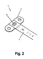
- the Fig. 1 and 2 show an arrangement 1, comprising at least one busbar 2, which forms a composite with at least one flexible circuit carrier 3, wherein the flexible circuit carrier 3 has at least one conductor track 4.
- the conductor 4 is welded to the busbar 2.
- the conductor 4 is ultrasonically welded to the busbar 2.
- the busbar 2 is made of metal.
- the conductor track 4 is made of copper and was at the back with a material-removing method, in particular by lasing, free of foil to allow access for the ultrasonic welding.
- the flexible circuit carrier 3 comprises at least one foil and conductor tracks 4.
- Fig. 3 shows an arrangement 1 'with a plurality of busbars 2 made of metal, which forms a composite with a circuit substrate 3' with a plurality of interconnects 4.
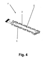
- Fig. 4 shows the arrangement 1 'according to Fig. 3 with a plurality of current busbars 2 made of metal, which forms a composite with a circuit carrier 3 'with a plurality of conductor tracks 4.
- a carrier film 5 On the flexible circuit substrate 3 'is a carrier film 5.
Landscapes
- Multi-Conductor Connections (AREA)
- Electric Connection Of Electric Components To Printed Circuits (AREA)
Abstract
Description
- Die Erfindung betrifft eine Anordnung gemäß dem Oberbegriff des Patentanspruchs 1.
- Aus der
DE 31 37 117 A1 ist eine Anordnung bekannt, bei welcher eine Stromsammelschiene mit mindestens einem Anschlußdraht einen Verbund bildet. Zur Herstellung des Verbunds ist eine Klemmschraube vorgesehen. - Die Herstellung der bisher bekannten Anordnungen ist kostenintensiv.
- Der Erfindung liegt daher die Aufgabe zugrunde, Material- und Prozesskosten zu reduzieren.
- Die vorliegende Erfindung löst die zuvor genannte Aufgabe durch eine Anordnung mit den Merkmalen des Patentanspruchs 1.
- Erfindungsgemäß ist erkannt worden, dass durch eine direkte Anbindung von Schaltungsträgern an Stromsammelschienen nahezu jeder Bereich der Schaltungsträger mit anderen Bauteilen und/ oder Baugruppen verbunden werden kann. Erfindungsgemäß werden Kontaktstellen mechanisch durch einen Folienverbund verstärkt bzw. gegen Belastungen unterstützt. Durch die verbundartige Anordnung, welche durch Ultraschallweißen gefertigt ist, kann nahezu jede Stelle der Schaltungsträger mit einem zu verbindenden Partner direkt elektrisch und/ oder mechanisch platzsparend kontaktiert werden. Hierbei können Kontaktteile eingespart werden. Auf Crimpverbindungen mit Schweißcrimps, welche aufgrund von Platzproblemen häufig nicht einsetzbar sind, wird verzichtet. Überdies werden durch den Verbund die Kontaktstellen mechanisch gefestigt bzw. verstärkt. Dies macht die Kontaktstellen widerstandsfähiger gegen Belastungen. Hierdurch werden zusätzliche Bauteile, insbesondere Kontaktteile, eingespart und Prozesskosten gesenkt.
- Folglich ist die eingangsgenannte Aufgabe gelöst.
- Die Leiterbahn könnte mit der Stromsammelschiene ultraschallverschweißt sein. Durch Ultraschallverschweißen können punktuell sehr eng definierte Bereiche erwärmt werden. Hierfür ist die Leiterbahn rückseitig von Folie befreit.
- Die Stromsammelschiene könnte zwischen zwei Schaltungsträgern einlaminiert sein. Hierdurch wird ein besonders fester Verbund erzielt.
- Auf dem flexiblen Schaltungsträger könnte eine Trägerfolie aufliegen. Durch diese konstruktive Maßnahme wird die Anordnung verstärkt.
- Der hier beschriebene flexible Schaltungsträger ist vorzugsweise als flaches Element ausgebildet, welches auf mindestens einer Folie oder zwischen zwei Folien Leiterbahnen und/ oder elektrische Schaltungen aufweist.
- Es könnte eine Bestückung mit passiven elektronischen Bauteilen vorgesehen sein, welche über Lötstellen mit dem Schaltungsträger kontaktiert sind. Ein Verbund kann passive elektronische Bauteile, wie Sicherungen und Temperatursensoren tragen, welche über Lötstellen mit dem Schaltungsträger kontaktiert werden.
- Die hier beschriebene Anordnung ist in mechatronischen Baugruppen für Batterieanwendungen verwendbar. Denkbar sind sämtliche Verwendungen in der Folientechnologie, bei welchen elektrische und/ oder mechanische Kontaktierungen von Folien mit anderen Bauteilen und/ oder Baugruppen durchgeführt werden.
- In der Zeichnung zeigen
- Fig. 1
- eine schematische Ansicht einer Anordnung, welche einen Verbund aus einer Sammelschiene und einem flexiblen Schaltungsträger umfasst,
- Fig. 2
- eine rückseitige Ansicht der Anordnung gemäß
Fig. 1 , - Fig. 3
- eine weitere Anordnung mit mehreren Sammelschienen und
- Fig. 4
- eine rückseitige Ansicht der Anordnung gemäß
Fig. 3 , bei welcher der flexible Schaltungsträger zur Verstärkung mit einer Trägerfolie versehen ist. - Die
Fig. 1 und2 zeigen eine Anordnung 1, umfassend mindestens eine Stromsammelschiene 2, welche mit mindestens einem flexiblen Schaltungsträger 3 einen Verbund bildet, wobei der flexible Schaltungsträger 3 mindestens eine Leiterbahn 4 aufweist. - Die Leiterbahn 4 ist mit der Stromsammelschiene 2 verschweißt. Die Leiterbahn 4 ist mit der Stromsammelschiene 2 ultraschallverschweißt.
- Die Stromsammelschiene 2 ist aus Metall gefertigt. Die Leiterbahn 4 ist aus Kupfer gefertigt und wurde rückseitig mit einem materialabtragenden Verfahren, insbesondere durch Lasern, von Folie befreit, um einen Zugang für das Ultraschallschweißen zu ermöglichen.
- Der flexible Schaltungsträger 3 umfasst mindestens eine Folie und Leiterbahnen 4.
-
Fig. 3 zeigt eine Anordnung 1' mit mehreren Stromsammelschienen 2 aus Metall, welche einen Verbund mit einem Schaltungsträger 3' mit mehreren Leiterbahnen 4 bildet. -
Fig. 4 zeigt die Anordnung 1' gemäßFig. 3 mit mehreren Stromsammelschienen 2 aus Metall, welche einen Verbund mit einem Schaltungsträger 3' mit mehreren Leiterbahnen 4 bildet. Auf dem flexiblen Schaltungsträger 3' liegt eine Trägerfolie 5 auf.
Claims (5)
- Anordnung (1, 1'), umfassend mindestens eine Stromsammelschiene (2), welche mit mindestens einem flexiblen Schaltungsträger (3, 3') einen Verbund bildet, wobei der flexible Schaltungsträger (3, 3') mindestens eine Leiterbahn (4) aufweist,
dadurch gekennzeichnet, dass die Leiterbahn (4) mit der Stromsammelschiene (2) verschweißt ist. - Anordnung nach Anspruch 1, dadurch gekennzeichnet, dass die Leiterbahn (4) mit der Stromsammelschiene (2) ultraschallverschweißt ist.
- Anordnung nach Anspruch 1 oder 2, dadurch gekennzeichnet, dass die Stromsammelschiene (2) zwischen zwei Schaltungsträgern (3, 3') einlaminiert ist.
- Anordnung nach einem der voranstehenden Ansprüche, dadurch gekennzeichnet, dass auf dem flexiblen Schaltungsträger (3, 3') eine Trägerfolie (5) aufliegt.
- Anordnung nach einem der voranstehenden Ansprüche, dadurch gekennzeichnet, dass eine Bestückung mit passiven elektronischen Bauteilen vorgesehen ist, welche über Lötstellen mit dem Schaltungsträger (3, 3') kontaktiert sind.
Applications Claiming Priority (1)
| Application Number | Priority Date | Filing Date | Title |
|---|---|---|---|
| DE102012015215.9A DE102012015215B3 (de) | 2012-08-03 | 2012-08-03 | Anordnung mit Stromsammelschienen |
Publications (2)
| Publication Number | Publication Date |
|---|---|
| EP2693571A1 true EP2693571A1 (de) | 2014-02-05 |
| EP2693571B1 EP2693571B1 (de) | 2017-05-10 |
Family
ID=48470686
Family Applications (1)
| Application Number | Title | Priority Date | Filing Date |
|---|---|---|---|
| EP13002591.9A Active EP2693571B1 (de) | 2012-08-03 | 2013-05-16 | Anordnung mit Stromsammelschienen |
Country Status (3)
| Country | Link |
|---|---|
| US (1) | US20140036457A1 (de) |
| EP (1) | EP2693571B1 (de) |
| DE (1) | DE102012015215B3 (de) |
Families Citing this family (1)
| Publication number | Priority date | Publication date | Assignee | Title |
|---|---|---|---|---|
| JP2016163409A (ja) * | 2015-02-27 | 2016-09-05 | 日本電産株式会社 | モータ |
Citations (4)
| Publication number | Priority date | Publication date | Assignee | Title |
|---|---|---|---|---|
| BE737653A (de) * | 1969-08-19 | 1970-02-02 | ||
| DE3137117A1 (de) | 1981-09-18 | 1983-04-14 | Brown, Boveri & Cie Ag, 6800 Mannheim | "schraubklemme" |
| US20010015347A1 (en) * | 2000-02-23 | 2001-08-23 | Ichiro Terunuma | Connection structure and method for connecting printed circuit and metal terminal, and reinforcing structure and method for reinforcing junction therebetween |
| EP1253684A2 (de) * | 2001-04-25 | 2002-10-30 | Autonetworks Technologies, Ltd. | Verdrahtungsmaterial und sein Herstellungsverfahren |
Family Cites Families (14)
| Publication number | Priority date | Publication date | Assignee | Title |
|---|---|---|---|---|
| US5805402A (en) * | 1993-06-09 | 1998-09-08 | Ut Automotive Dearborn, Inc. | Integrated interior trim and electrical assembly for an automotive vehicle |
| JP2000182682A (ja) * | 1998-12-18 | 2000-06-30 | Sumitomo Wiring Syst Ltd | 電気接続箱 |
| EP1061606A3 (de) * | 1999-06-16 | 2004-05-19 | Sumitomo Wiring Systems, Ltd. | Anordnung und Verfahren zum Verbinden eines Flachkabels mit Sammelschienen |
| DE60033425D1 (de) * | 1999-12-10 | 2007-03-29 | Thermion Systems Int | Thermoplastische mehrschicht- gewebeheizung und verfahren zu deren herstellung |
| JP2002042924A (ja) * | 2000-07-28 | 2002-02-08 | Sumitomo Wiring Syst Ltd | 電気接続構造 |
| JP4013691B2 (ja) * | 2002-07-31 | 2007-11-28 | 住友電装株式会社 | フレキシブルフラットケーブルの接続方法および超音波溶接機 |
| ATE353539T1 (de) * | 2004-04-16 | 2007-02-15 | Delphi Tech Inc | Verfahren zur kontaktierung eines elektrischen bauelements auf einem flexiblen schaltungsträger und flexibler schaltungsträger mit einem darauf kontaktierten elektrischen baulelement |
| EP2383840B1 (de) * | 2005-02-03 | 2016-04-13 | Auto-Kabel Management GmbH | Elektrischer Flachbandleiter für Kraftfahrzeuge |
| US20080010815A1 (en) * | 2006-07-17 | 2008-01-17 | W.E.T. Automotive Group Ag | Heating tape structure |
| EP2325920A3 (de) * | 2009-10-30 | 2011-12-07 | Sanyo Electric Co., Ltd. | Batteriesystem und dieses enthaltendes Elektrofahrzeug |
| JP2011210710A (ja) * | 2010-03-12 | 2011-10-20 | Autonetworks Technologies Ltd | 電池モジュール |
| DE112012002847B4 (de) * | 2011-07-04 | 2024-06-20 | Yazaki Corporation | Flachkabel-Wasserabdichtungssteckverbinder und Wasserabdichtungssteckverbinderaufbau für Flachkabel |
| JP5792011B2 (ja) * | 2011-09-26 | 2015-10-07 | 矢崎総業株式会社 | フラットケーブル防水コネクタ構造、及びその接続方法 |
| US9178203B2 (en) * | 2012-02-15 | 2015-11-03 | GM Global Technology Operations LLC | Battery module with a flexible bus |
-
2012
- 2012-08-03 DE DE102012015215.9A patent/DE102012015215B3/de active Active
-
2013
- 2013-05-16 EP EP13002591.9A patent/EP2693571B1/de active Active
- 2013-08-01 US US13/956,468 patent/US20140036457A1/en not_active Abandoned
Patent Citations (4)
| Publication number | Priority date | Publication date | Assignee | Title |
|---|---|---|---|---|
| BE737653A (de) * | 1969-08-19 | 1970-02-02 | ||
| DE3137117A1 (de) | 1981-09-18 | 1983-04-14 | Brown, Boveri & Cie Ag, 6800 Mannheim | "schraubklemme" |
| US20010015347A1 (en) * | 2000-02-23 | 2001-08-23 | Ichiro Terunuma | Connection structure and method for connecting printed circuit and metal terminal, and reinforcing structure and method for reinforcing junction therebetween |
| EP1253684A2 (de) * | 2001-04-25 | 2002-10-30 | Autonetworks Technologies, Ltd. | Verdrahtungsmaterial und sein Herstellungsverfahren |
Also Published As
| Publication number | Publication date |
|---|---|
| EP2693571B1 (de) | 2017-05-10 |
| DE102012015215B3 (de) | 2014-02-20 |
| US20140036457A1 (en) | 2014-02-06 |
Similar Documents
| Publication | Publication Date | Title |
|---|---|---|
| EP2274749B1 (de) | Elektronisches bauelement und entsprechendes herstellungsverfahren | |
| DE102008023451B4 (de) | Elektrische Verbindungsanordnung als Stromverteilungsschaltung | |
| DE69331676T2 (de) | Hochstromleiterplatte | |
| DE112015004819T5 (de) | Filmartige Leiterplatte und Verfahren zur Herstellung derselbigen | |
| DE102011004526B4 (de) | Leiterplatte mit hoher Stromtragfähigkeit und Verfahren zur Herstellung einer solchen Leiterplatte | |
| DE112016005794T5 (de) | Schaltungsanordnung und elektrischer Anschlusskasten | |
| DE102019100106A1 (de) | Einpressbares leistungsmodul und zugehörige verfahren | |
| DE102019125108A1 (de) | Leistungselektronikanordnung umfassend eine Leiterplatte und ein Leistungsmodul, Verfahren zur Herstellung einer Leistungselektronikanordnung, Kraftfahrzeug umfassend eine Leistungselektronikanordnung | |
| EP2434846B1 (de) | Verdrahtungselement, Leistungsverteiler und Fahrzeugbatterie | |
| DE102012008514A1 (de) | Leiterplatte mit hochbelastbarem Strompfad | |
| EP2693571B1 (de) | Anordnung mit Stromsammelschienen | |
| DE102013016073B4 (de) | Vorrichtung zur Signalübertragung in einem Fahrzeug | |
| DE102019204639A1 (de) | Luftspaltbildung in einer elektrischen Kontaktierung einer Leiterplatte | |
| DE102018129878A1 (de) | Verfahren und Hülse zum Verbinden leistungselektronischer Bauelemente und Leiterplatten | |
| DE102016110847B4 (de) | Leitungsintegrierter Schalter und Verfahren zum Herstellen eines leitungsintegrierten Schalters | |
| DE102009016842B4 (de) | Leitungsgitter für Elektronikgehäuse und Herstellungsverfahren | |
| DE102013021571A1 (de) | Kontaktiereinrichtung für einen Kraftwagen sowie Verfahren zum Herstellen einer solchen Kontaktiereinrichtung | |
| DE102008052925A1 (de) | Schnittstelle von Sammelschiene mit gedruckter Leiterplatte für Elektro- und Hybridelektrofahrzeuge | |
| EP2880716A1 (de) | Belastungsminimierende elektrische durchkontaktierung | |
| DE112017007766B4 (de) | Halbleitereinrichtung | |
| EP2285197A1 (de) | Verfahren zur Verbindung eines elektronischen Bauteils mit einer Leiterplatte | |
| EP4222817A1 (de) | Elektrische leitungsverbindung zur elektrischen kontaktierung einer flächenelektrode | |
| DE102012216785A1 (de) | Kontaktanordnung für einen mehrlagigen Schaltungsträger und Verfahren zum Kontaktieren eines mehrlagigen Schaltungsträgers | |
| DE102018003510B4 (de) | Elektrisches Gerät | |
| DE10228756A1 (de) | Leiterplatte, Leiterplattenanordnung und Verwendung der Leiterplatte |
Legal Events
| Date | Code | Title | Description |
|---|---|---|---|
| AK | Designated contracting states |
Kind code of ref document: A1 Designated state(s): AL AT BE BG CH CY CZ DE DK EE ES FI FR GB GR HR HU IE IS IT LI LT LU LV MC MK MT NL NO PL PT RO RS SE SI SK SM TR |
|
| AX | Request for extension of the european patent |
Extension state: BA ME |
|
| PUAI | Public reference made under article 153(3) epc to a published international application that has entered the european phase |
Free format text: ORIGINAL CODE: 0009012 |
|
| 17P | Request for examination filed |
Effective date: 20140523 |
|
| RBV | Designated contracting states (corrected) |
Designated state(s): AL AT BE BG CH CY CZ DE DK EE ES FI FR GB GR HR HU IE IS IT LI LT LU LV MC MK MT NL NO PL PT RO RS SE SI SK SM TR |
|
| RAP1 | Party data changed (applicant data changed or rights of an application transferred) |
Owner name: MEKTEC EUROPE GMBH |
|
| GRAP | Despatch of communication of intention to grant a patent |
Free format text: ORIGINAL CODE: EPIDOSNIGR1 |
|
| STAA | Information on the status of an ep patent application or granted ep patent |
Free format text: STATUS: GRANT OF PATENT IS INTENDED |
|
| INTG | Intention to grant announced |
Effective date: 20170220 |
|
| GRAS | Grant fee paid |
Free format text: ORIGINAL CODE: EPIDOSNIGR3 |
|
| GRAA | (expected) grant |
Free format text: ORIGINAL CODE: 0009210 |
|
| STAA | Information on the status of an ep patent application or granted ep patent |
Free format text: STATUS: THE PATENT HAS BEEN GRANTED |
|
| AK | Designated contracting states |
Kind code of ref document: B1 Designated state(s): AL AT BE BG CH CY CZ DE DK EE ES FI FR GB GR HR HU IE IS IT LI LT LU LV MC MK MT NL NO PL PT RO RS SE SI SK SM TR |
|
| REG | Reference to a national code |
Ref country code: GB Ref legal event code: FG4D Free format text: NOT ENGLISH |
|
| REG | Reference to a national code |
Ref country code: AT Ref legal event code: REF Ref document number: 893220 Country of ref document: AT Kind code of ref document: T Effective date: 20170515 Ref country code: CH Ref legal event code: EP |
|
| REG | Reference to a national code |
Ref country code: IE Ref legal event code: FG4D Free format text: LANGUAGE OF EP DOCUMENT: GERMAN |
|
| REG | Reference to a national code |
Ref country code: DE Ref legal event code: R096 Ref document number: 502013007184 Country of ref document: DE |
|
| REG | Reference to a national code |
Ref country code: NL Ref legal event code: MP Effective date: 20170510 |
|
| REG | Reference to a national code |
Ref country code: LT Ref legal event code: MG4D |
|
| PG25 | Lapsed in a contracting state [announced via postgrant information from national office to epo] |
Ref country code: NO Free format text: LAPSE BECAUSE OF FAILURE TO SUBMIT A TRANSLATION OF THE DESCRIPTION OR TO PAY THE FEE WITHIN THE PRESCRIBED TIME-LIMIT Effective date: 20170810 Ref country code: LT Free format text: LAPSE BECAUSE OF FAILURE TO SUBMIT A TRANSLATION OF THE DESCRIPTION OR TO PAY THE FEE WITHIN THE PRESCRIBED TIME-LIMIT Effective date: 20170510 Ref country code: FI Free format text: LAPSE BECAUSE OF FAILURE TO SUBMIT A TRANSLATION OF THE DESCRIPTION OR TO PAY THE FEE WITHIN THE PRESCRIBED TIME-LIMIT Effective date: 20170510 Ref country code: GR Free format text: LAPSE BECAUSE OF FAILURE TO SUBMIT A TRANSLATION OF THE DESCRIPTION OR TO PAY THE FEE WITHIN THE PRESCRIBED TIME-LIMIT Effective date: 20170811 Ref country code: HR Free format text: LAPSE BECAUSE OF FAILURE TO SUBMIT A TRANSLATION OF THE DESCRIPTION OR TO PAY THE FEE WITHIN THE PRESCRIBED TIME-LIMIT Effective date: 20170510 Ref country code: ES Free format text: LAPSE BECAUSE OF FAILURE TO SUBMIT A TRANSLATION OF THE DESCRIPTION OR TO PAY THE FEE WITHIN THE PRESCRIBED TIME-LIMIT Effective date: 20170510 |
|
| PG25 | Lapsed in a contracting state [announced via postgrant information from national office to epo] |
Ref country code: LV Free format text: LAPSE BECAUSE OF FAILURE TO SUBMIT A TRANSLATION OF THE DESCRIPTION OR TO PAY THE FEE WITHIN THE PRESCRIBED TIME-LIMIT Effective date: 20170510 Ref country code: NL Free format text: LAPSE BECAUSE OF FAILURE TO SUBMIT A TRANSLATION OF THE DESCRIPTION OR TO PAY THE FEE WITHIN THE PRESCRIBED TIME-LIMIT Effective date: 20170510 Ref country code: PL Free format text: LAPSE BECAUSE OF FAILURE TO SUBMIT A TRANSLATION OF THE DESCRIPTION OR TO PAY THE FEE WITHIN THE PRESCRIBED TIME-LIMIT Effective date: 20170510 Ref country code: RS Free format text: LAPSE BECAUSE OF FAILURE TO SUBMIT A TRANSLATION OF THE DESCRIPTION OR TO PAY THE FEE WITHIN THE PRESCRIBED TIME-LIMIT Effective date: 20170510 Ref country code: SE Free format text: LAPSE BECAUSE OF FAILURE TO SUBMIT A TRANSLATION OF THE DESCRIPTION OR TO PAY THE FEE WITHIN THE PRESCRIBED TIME-LIMIT Effective date: 20170510 Ref country code: BG Free format text: LAPSE BECAUSE OF FAILURE TO SUBMIT A TRANSLATION OF THE DESCRIPTION OR TO PAY THE FEE WITHIN THE PRESCRIBED TIME-LIMIT Effective date: 20170810 Ref country code: IS Free format text: LAPSE BECAUSE OF FAILURE TO SUBMIT A TRANSLATION OF THE DESCRIPTION OR TO PAY THE FEE WITHIN THE PRESCRIBED TIME-LIMIT Effective date: 20170910 |
|
| REG | Reference to a national code |
Ref country code: CH Ref legal event code: PL |
|
| PG25 | Lapsed in a contracting state [announced via postgrant information from national office to epo] |
Ref country code: EE Free format text: LAPSE BECAUSE OF FAILURE TO SUBMIT A TRANSLATION OF THE DESCRIPTION OR TO PAY THE FEE WITHIN THE PRESCRIBED TIME-LIMIT Effective date: 20170510 Ref country code: CZ Free format text: LAPSE BECAUSE OF FAILURE TO SUBMIT A TRANSLATION OF THE DESCRIPTION OR TO PAY THE FEE WITHIN THE PRESCRIBED TIME-LIMIT Effective date: 20170510 Ref country code: SK Free format text: LAPSE BECAUSE OF FAILURE TO SUBMIT A TRANSLATION OF THE DESCRIPTION OR TO PAY THE FEE WITHIN THE PRESCRIBED TIME-LIMIT Effective date: 20170510 Ref country code: DK Free format text: LAPSE BECAUSE OF FAILURE TO SUBMIT A TRANSLATION OF THE DESCRIPTION OR TO PAY THE FEE WITHIN THE PRESCRIBED TIME-LIMIT Effective date: 20170510 Ref country code: RO Free format text: LAPSE BECAUSE OF FAILURE TO SUBMIT A TRANSLATION OF THE DESCRIPTION OR TO PAY THE FEE WITHIN THE PRESCRIBED TIME-LIMIT Effective date: 20170510 |
|
| REG | Reference to a national code |
Ref country code: DE Ref legal event code: R097 Ref document number: 502013007184 Country of ref document: DE |
|
| REG | Reference to a national code |
Ref country code: IE Ref legal event code: MM4A |
|
| PG25 | Lapsed in a contracting state [announced via postgrant information from national office to epo] |
Ref country code: IT Free format text: LAPSE BECAUSE OF FAILURE TO SUBMIT A TRANSLATION OF THE DESCRIPTION OR TO PAY THE FEE WITHIN THE PRESCRIBED TIME-LIMIT Effective date: 20170510 Ref country code: SM Free format text: LAPSE BECAUSE OF FAILURE TO SUBMIT A TRANSLATION OF THE DESCRIPTION OR TO PAY THE FEE WITHIN THE PRESCRIBED TIME-LIMIT Effective date: 20170510 Ref country code: LI Free format text: LAPSE BECAUSE OF NON-PAYMENT OF DUE FEES Effective date: 20170531 Ref country code: CH Free format text: LAPSE BECAUSE OF NON-PAYMENT OF DUE FEES Effective date: 20170531 |
|
| PLBE | No opposition filed within time limit |
Free format text: ORIGINAL CODE: 0009261 |
|
| STAA | Information on the status of an ep patent application or granted ep patent |
Free format text: STATUS: NO OPPOSITION FILED WITHIN TIME LIMIT |
|
| PG25 | Lapsed in a contracting state [announced via postgrant information from national office to epo] |
Ref country code: LU Free format text: LAPSE BECAUSE OF NON-PAYMENT OF DUE FEES Effective date: 20170516 |
|
| 26N | No opposition filed |
Effective date: 20180213 |
|
| GBPC | Gb: european patent ceased through non-payment of renewal fee |
Effective date: 20170810 |
|
| REG | Reference to a national code |
Ref country code: BE Ref legal event code: MM Effective date: 20170531 |
|
| PG25 | Lapsed in a contracting state [announced via postgrant information from national office to epo] |
Ref country code: IE Free format text: LAPSE BECAUSE OF NON-PAYMENT OF DUE FEES Effective date: 20170516 |
|
| REG | Reference to a national code |
Ref country code: FR Ref legal event code: ST Effective date: 20180406 |
|
| PG25 | Lapsed in a contracting state [announced via postgrant information from national office to epo] |
Ref country code: SI Free format text: LAPSE BECAUSE OF FAILURE TO SUBMIT A TRANSLATION OF THE DESCRIPTION OR TO PAY THE FEE WITHIN THE PRESCRIBED TIME-LIMIT Effective date: 20170510 |
|
| PG25 | Lapsed in a contracting state [announced via postgrant information from national office to epo] |
Ref country code: GB Free format text: LAPSE BECAUSE OF NON-PAYMENT OF DUE FEES Effective date: 20170810 |
|
| PG25 | Lapsed in a contracting state [announced via postgrant information from national office to epo] |
Ref country code: FR Free format text: LAPSE BECAUSE OF NON-PAYMENT OF DUE FEES Effective date: 20170710 Ref country code: BE Free format text: LAPSE BECAUSE OF NON-PAYMENT OF DUE FEES Effective date: 20170531 |
|
| PG25 | Lapsed in a contracting state [announced via postgrant information from national office to epo] |
Ref country code: MT Free format text: LAPSE BECAUSE OF FAILURE TO SUBMIT A TRANSLATION OF THE DESCRIPTION OR TO PAY THE FEE WITHIN THE PRESCRIBED TIME-LIMIT Effective date: 20170510 |
|
| PG25 | Lapsed in a contracting state [announced via postgrant information from national office to epo] |
Ref country code: HU Free format text: LAPSE BECAUSE OF FAILURE TO SUBMIT A TRANSLATION OF THE DESCRIPTION OR TO PAY THE FEE WITHIN THE PRESCRIBED TIME-LIMIT; INVALID AB INITIO Effective date: 20130516 Ref country code: MC Free format text: LAPSE BECAUSE OF FAILURE TO SUBMIT A TRANSLATION OF THE DESCRIPTION OR TO PAY THE FEE WITHIN THE PRESCRIBED TIME-LIMIT Effective date: 20170510 |
|
| REG | Reference to a national code |
Ref country code: AT Ref legal event code: MM01 Ref document number: 893220 Country of ref document: AT Kind code of ref document: T Effective date: 20180516 |
|
| PG25 | Lapsed in a contracting state [announced via postgrant information from national office to epo] |
Ref country code: AT Free format text: LAPSE BECAUSE OF NON-PAYMENT OF DUE FEES Effective date: 20180516 Ref country code: CY Free format text: LAPSE BECAUSE OF NON-PAYMENT OF DUE FEES Effective date: 20170510 |
|
| PG25 | Lapsed in a contracting state [announced via postgrant information from national office to epo] |
Ref country code: MK Free format text: LAPSE BECAUSE OF FAILURE TO SUBMIT A TRANSLATION OF THE DESCRIPTION OR TO PAY THE FEE WITHIN THE PRESCRIBED TIME-LIMIT Effective date: 20170510 |
|
| PG25 | Lapsed in a contracting state [announced via postgrant information from national office to epo] |
Ref country code: TR Free format text: LAPSE BECAUSE OF FAILURE TO SUBMIT A TRANSLATION OF THE DESCRIPTION OR TO PAY THE FEE WITHIN THE PRESCRIBED TIME-LIMIT Effective date: 20170510 |
|
| PG25 | Lapsed in a contracting state [announced via postgrant information from national office to epo] |
Ref country code: PT Free format text: LAPSE BECAUSE OF FAILURE TO SUBMIT A TRANSLATION OF THE DESCRIPTION OR TO PAY THE FEE WITHIN THE PRESCRIBED TIME-LIMIT Effective date: 20170510 |
|
| PG25 | Lapsed in a contracting state [announced via postgrant information from national office to epo] |
Ref country code: AL Free format text: LAPSE BECAUSE OF FAILURE TO SUBMIT A TRANSLATION OF THE DESCRIPTION OR TO PAY THE FEE WITHIN THE PRESCRIBED TIME-LIMIT Effective date: 20170510 |
|
| PGFP | Annual fee paid to national office [announced via postgrant information from national office to epo] |
Ref country code: DE Payment date: 20250519 Year of fee payment: 13 |
|
| REG | Reference to a national code |
Ref country code: DE Ref legal event code: R082 Ref document number: 502013007184 Country of ref document: DE Representative=s name: WESCH, ARNO, DR. RER. NAT., DE |