EP2688074A1 - Magnetic module for power inductor, power inductor, and manufacturing method thereof - Google Patents
Magnetic module for power inductor, power inductor, and manufacturing method thereof Download PDFInfo
- Publication number
- EP2688074A1 EP2688074A1 EP13275063.9A EP13275063A EP2688074A1 EP 2688074 A1 EP2688074 A1 EP 2688074A1 EP 13275063 A EP13275063 A EP 13275063A EP 2688074 A1 EP2688074 A1 EP 2688074A1
- Authority
- EP
- European Patent Office
- Prior art keywords
- support layer
- coil support
- coil
- substrate
- recess
- Prior art date
- Legal status (The legal status is an assumption and is not a legal conclusion. Google has not performed a legal analysis and makes no representation as to the accuracy of the status listed.)
- Granted
Links
- 238000004519 manufacturing process Methods 0.000 title claims description 9
- 239000000758 substrate Substances 0.000 claims description 45
- 239000000696 magnetic material Substances 0.000 claims description 10
- 238000000034 method Methods 0.000 claims description 9
- 239000011810 insulating material Substances 0.000 claims description 8
- 230000035699 permeability Effects 0.000 claims description 5
- 238000010030 laminating Methods 0.000 claims description 4
- 239000011159 matrix material Substances 0.000 claims description 3
- PXHVJJICTQNCMI-UHFFFAOYSA-N Nickel Chemical compound [Ni] PXHVJJICTQNCMI-UHFFFAOYSA-N 0.000 description 12
- KDLHZDBZIXYQEI-UHFFFAOYSA-N Palladium Chemical compound [Pd] KDLHZDBZIXYQEI-UHFFFAOYSA-N 0.000 description 12
- 229910052751 metal Inorganic materials 0.000 description 12
- 239000002184 metal Substances 0.000 description 12
- BASFCYQUMIYNBI-UHFFFAOYSA-N platinum Chemical compound [Pt] BASFCYQUMIYNBI-UHFFFAOYSA-N 0.000 description 12
- 239000000463 material Substances 0.000 description 10
- 229910000859 α-Fe Inorganic materials 0.000 description 9
- 239000010949 copper Substances 0.000 description 8
- 239000010931 gold Substances 0.000 description 8
- 239000010409 thin film Substances 0.000 description 7
- 230000004907 flux Effects 0.000 description 6
- 229920000642 polymer Polymers 0.000 description 6
- 238000004804 winding Methods 0.000 description 5
- RYGMFSIKBFXOCR-UHFFFAOYSA-N Copper Chemical compound [Cu] RYGMFSIKBFXOCR-UHFFFAOYSA-N 0.000 description 4
- BQCADISMDOOEFD-UHFFFAOYSA-N Silver Chemical compound [Ag] BQCADISMDOOEFD-UHFFFAOYSA-N 0.000 description 4
- 229910045601 alloy Inorganic materials 0.000 description 4
- 239000000956 alloy Substances 0.000 description 4
- 230000015556 catabolic process Effects 0.000 description 4
- 229910052802 copper Inorganic materials 0.000 description 4
- 238000006731 degradation reaction Methods 0.000 description 4
- PCHJSUWPFVWCPO-UHFFFAOYSA-N gold Chemical compound [Au] PCHJSUWPFVWCPO-UHFFFAOYSA-N 0.000 description 4
- 229910052737 gold Inorganic materials 0.000 description 4
- 229910052759 nickel Inorganic materials 0.000 description 4
- 229910052763 palladium Inorganic materials 0.000 description 4
- 229910052697 platinum Inorganic materials 0.000 description 4
- 229910052709 silver Inorganic materials 0.000 description 4
- 239000004332 silver Substances 0.000 description 4
- 230000008859 change Effects 0.000 description 3
- 239000002131 composite material Substances 0.000 description 3
- 238000005520 cutting process Methods 0.000 description 3
- 230000004048 modification Effects 0.000 description 3
- 238000012986 modification Methods 0.000 description 3
- 239000004020 conductor Substances 0.000 description 2
- 230000003247 decreasing effect Effects 0.000 description 2
- 238000003475 lamination Methods 0.000 description 2
- 239000006247 magnetic powder Substances 0.000 description 2
- 230000005415 magnetization Effects 0.000 description 2
- 230000000149 penetrating effect Effects 0.000 description 2
- KOMIMHZRQFFCOR-UHFFFAOYSA-N [Ni].[Cu].[Zn] Chemical compound [Ni].[Cu].[Zn] KOMIMHZRQFFCOR-UHFFFAOYSA-N 0.000 description 1
- 239000003990 capacitor Substances 0.000 description 1
- 238000005266 casting Methods 0.000 description 1
- 238000004891 communication Methods 0.000 description 1
- 238000000151 deposition Methods 0.000 description 1
- 239000012777 electrically insulating material Substances 0.000 description 1
- 230000001788 irregular Effects 0.000 description 1
- 150000002739 metals Chemical class 0.000 description 1
- 238000007639 printing Methods 0.000 description 1
- 238000004080 punching Methods 0.000 description 1
- 230000009467 reduction Effects 0.000 description 1
- 238000004544 sputter deposition Methods 0.000 description 1
Images



Classifications
-
- H—ELECTRICITY
- H01—ELECTRIC ELEMENTS
- H01F—MAGNETS; INDUCTANCES; TRANSFORMERS; SELECTION OF MATERIALS FOR THEIR MAGNETIC PROPERTIES
- H01F5/00—Coils
-
- H—ELECTRICITY
- H01—ELECTRIC ELEMENTS
- H01F—MAGNETS; INDUCTANCES; TRANSFORMERS; SELECTION OF MATERIALS FOR THEIR MAGNETIC PROPERTIES
- H01F10/00—Thin magnetic films, e.g. of one-domain structure
- H01F10/08—Thin magnetic films, e.g. of one-domain structure characterised by magnetic layers
-
- H—ELECTRICITY
- H01—ELECTRIC ELEMENTS
- H01F—MAGNETS; INDUCTANCES; TRANSFORMERS; SELECTION OF MATERIALS FOR THEIR MAGNETIC PROPERTIES
- H01F17/00—Fixed inductances of the signal type
-
- H—ELECTRICITY
- H01—ELECTRIC ELEMENTS
- H01F—MAGNETS; INDUCTANCES; TRANSFORMERS; SELECTION OF MATERIALS FOR THEIR MAGNETIC PROPERTIES
- H01F17/00—Fixed inductances of the signal type
- H01F17/0006—Printed inductances
- H01F17/0013—Printed inductances with stacked layers
-
- H—ELECTRICITY
- H01—ELECTRIC ELEMENTS
- H01F—MAGNETS; INDUCTANCES; TRANSFORMERS; SELECTION OF MATERIALS FOR THEIR MAGNETIC PROPERTIES
- H01F41/00—Apparatus or processes specially adapted for manufacturing or assembling magnets, inductances or transformers; Apparatus or processes specially adapted for manufacturing materials characterised by their magnetic properties
- H01F41/02—Apparatus or processes specially adapted for manufacturing or assembling magnets, inductances or transformers; Apparatus or processes specially adapted for manufacturing materials characterised by their magnetic properties for manufacturing cores, coils, or magnets
- H01F41/04—Apparatus or processes specially adapted for manufacturing or assembling magnets, inductances or transformers; Apparatus or processes specially adapted for manufacturing materials characterised by their magnetic properties for manufacturing cores, coils, or magnets for manufacturing coils
-
- H—ELECTRICITY
- H01—ELECTRIC ELEMENTS
- H01F—MAGNETS; INDUCTANCES; TRANSFORMERS; SELECTION OF MATERIALS FOR THEIR MAGNETIC PROPERTIES
- H01F41/00—Apparatus or processes specially adapted for manufacturing or assembling magnets, inductances or transformers; Apparatus or processes specially adapted for manufacturing materials characterised by their magnetic properties
- H01F41/02—Apparatus or processes specially adapted for manufacturing or assembling magnets, inductances or transformers; Apparatus or processes specially adapted for manufacturing materials characterised by their magnetic properties for manufacturing cores, coils, or magnets
- H01F41/04—Apparatus or processes specially adapted for manufacturing or assembling magnets, inductances or transformers; Apparatus or processes specially adapted for manufacturing materials characterised by their magnetic properties for manufacturing cores, coils, or magnets for manufacturing coils
- H01F41/041—Printed circuit coils
- H01F41/046—Printed circuit coils structurally combined with ferromagnetic material
-
- H—ELECTRICITY
- H01—ELECTRIC ELEMENTS
- H01F—MAGNETS; INDUCTANCES; TRANSFORMERS; SELECTION OF MATERIALS FOR THEIR MAGNETIC PROPERTIES
- H01F17/00—Fixed inductances of the signal type
- H01F17/04—Fixed inductances of the signal type with magnetic core
-
- H—ELECTRICITY
- H01—ELECTRIC ELEMENTS
- H01F—MAGNETS; INDUCTANCES; TRANSFORMERS; SELECTION OF MATERIALS FOR THEIR MAGNETIC PROPERTIES
- H01F27/00—Details of transformers or inductances, in general
- H01F27/28—Coils; Windings; Conductive connections
- H01F27/29—Terminals; Tapping arrangements for signal inductances
- H01F27/292—Surface mounted devices
-
- Y—GENERAL TAGGING OF NEW TECHNOLOGICAL DEVELOPMENTS; GENERAL TAGGING OF CROSS-SECTIONAL TECHNOLOGIES SPANNING OVER SEVERAL SECTIONS OF THE IPC; TECHNICAL SUBJECTS COVERED BY FORMER USPC CROSS-REFERENCE ART COLLECTIONS [XRACs] AND DIGESTS
- Y10—TECHNICAL SUBJECTS COVERED BY FORMER USPC
- Y10T—TECHNICAL SUBJECTS COVERED BY FORMER US CLASSIFICATION
- Y10T29/00—Metal working
- Y10T29/49—Method of mechanical manufacture
- Y10T29/49002—Electrical device making
- Y10T29/4902—Electromagnet, transformer or inductor
Definitions
- the present invention relates to a magnetic module for a power inductor, a power inductor, and a manufacturing method thereof.
- An inductor is a key passive element constituting an electronic circuit, together with a resistor and a capacitor.
- An inductor is used in a component or the like, to cancel noise or form an LC resonance circuit.
- Inductors may be classified as winding type inductors, laminated type inductors, thin film type inductors, and the like.
- the winding type inductor may be formed by winding a coil around a ferrite core, or the like.
- the winding type inductor may have stray capacitance between coils, and accordingly, in the case of increasing the number of turns of a coil to obtain higher inductance, degradation in high frequency characteristics may be caused.
- a laminated type inductor may be formed by laminating a plurality of ferrite sheets.
- coil-like metal patterns are formed on respective ferrite sheets, and the coil-like metal patterns may be sequentially connected by a plurality of conductive vias provided in the ferrite sheets.
- the laminated type inductor is appropriate for mass-production and has excellent high frequency characteristics compared with a winding type inductor.
- metal patterns are formed of a material having a low saturation magnetization value, and when the laminated type inductor is manufactured to have a small size, the number of laminations of the metal patterns is limited, resulting in lowered DC superposition characteristics and a failure to obtain a sufficient current.
- a thin film type inductor may use a material having a high saturation magnetization value and even in the case that a thin film type inductor is manufactured to have a small size, an internal circuit pattern thereof may be easily formed in comparison to a laminated type inductor. Thus, recently, research into the thin film type inductor has been actively undertaken.
- a coil When a thin film type inductor is manufactured to be large, a coil may have a large thickness, thereby eliminating degradation in product characteristics due to an increase in series resistance.
- Patent Document 1 Korean Patent Laid Open Publication No. 2006-0061709
- An aspect of the present invention provides a power inductor capable of lowering series resistance while maintaining a certain level of inductance even in the case that the power inductor is small.
- a power inductor including: a main body; and first and second external electrodes formed on both end portions of the main body, wherein the main body includes: upper and lower cover layers; at least one coil support layer having a through hole formed in a center thereof, at least one first recess portion formed in both lateral surfaces thereof and a plurality of second recess portions formed in respective corners thereof, and disposed between the upper and lower cover layers; and first and second coil layers formed on both surfaces of the coil support layer and having respective one ends thereof connected to the first and second external electrodes.
- the coil support layer may have magnetic permeability of 80% or below.
- An area ratio of the through hole to all of the second recess portions may be 0.60 or greater.
- the first recess portion of the coil support layer may be formed as an elongated recess in a length direction of the coil support layer.
- the first recess portion of the coil support layer may include a plurality of recess portions spaced apart from each other in a length direction of the coil support layer.
- the first recess portion of the coil support layer may be formed to communicate with the second recess portions of the coil support layer.
- the coil support layer may be a substrate formed of an insulating material or a magnetic material.
- An insulating layer may be formed on a circumference of the first and second coil layers.
- a magnetic module for a power inductor including main bodies connected in a matrix form, wherein each of the main bodies includes: upper and lower cover layers; at least one coil support layer having a central through hole provided therein, at least one first recess portion formed in both lateral surfaces thereof and a plurality of second recess portions formed in respective corners thereof, and disposed between the upper and lower cover layers; and first and second coil layers formed on both surfaces of the coil support layer and having respective one ends exposed to the outside.
- a method of manufacturing a power inductor including: preparing a substrate formed of an insulating material or a magnetic material and having a through hole in a center thereof, at least one first recess portion formed in both lateral surfaces thereof, and a plurality of second recess portions formed in respective corners thereof; forming first and second coil layers on both surfaces of the substrate; disposing the substrate having the first and second coil layers formed thereon, on a lower cover layer; forming a main body by forming an upper cover layer on the substrate; and forming first and second external electrodes on both end portions of the main body such that the first and second external electrodes are connected to portions of the first and second coil layers led thereto.
- the substrate Before the disposing of the substrate, covering a circumference of the substrate having the first and second coil layers formed thereon, with an insulating material, may be performed.
- the disposing of the substrate may include laminating a plurality of substrates on the lower cover layer.
- the first recess portion may be formed as an elongated recess in a length direction of the coil support layer.
- both lateral surfaces of the substrate may be removed to leave only portions thereof to form a plurality of first recess portions spaced apart from each other.
- the first recess portion may be formed to communicate with the second recess portions.
- an inductor 1 includes a main body 10 and first and second external electrodes 21 and 22 formed on both end portions of the main body 10.
- an "L direction” is a “length direction”
- a "W direction” is a “width direction”
- a “T direction” is a “thickness direction” following directions of FIG. 1 .
- the main body 10 may have a rectangular parallelepiped shape and include upper and lower cover layers 11 and 12 formed of a magnetic material, a coil support layer 30 disposed between the upper and lower cover layers 11 and 12, and first and second coil layers 41 and 42 formed on both surfaces of the coil support layer 30 and having respective one ends electrically connected to the first and second external electrodes 21 and 22.
- the upper and lower cover layers 11 and 12 may formed as substrates formed of a paste including a composite of a ferrite or metallic magnetic powder and a polymer, or including a magnetic material such as a nickel-zinc-copper ferrite.
- the upper and lower cover layers 11 and 12 may serve to prevent basic electrical characteristics of the first and second coil layers 41 and 42 from being degraded.
- the first and second external electrodes 21 and 22 may include a metal capable of providing electrical conductivity.
- the first and second external electrodes 21 and 22 may include at least one metal selected from the group consisting of gold (Au), silver (Ag), platinum (Pt), copper (Cu), nickel (Ni), palladium (Pd), and alloys thereof.
- a nickel-plated layer (not shown) or a tin-plated layer (not shown) may be further formed on a surface of the first and second external electrodes 21 and 22 as necessary.
- the coil support layer 30 may be fabricated as a substrate formed of, for example, an electrically insulating material such as a photosensitive polymer, or a magnetic material such as ferrite, or the like.
- a photosensitive insulating material may be interposed between the first and second coil layers 41 and 42 adjacent to each other, and the first and second coil layers 41 and 42 may be electrically connected by a conductive via (not shown).
- the conductive via may be formed by forming a through hole (not shown) penetrating the coil support layer 30 in a thickness direction, and filling the through hole with a conductive paste, or the like.
- the number of turns of the first and second coil layers 41 and 42 should be increased or a length of the first and second coil layers 41 and 42 should be increased.
- resistance may be increased.
- resistance may be increased in proportion thereto.
- a structure of decreasing the length of the first and second coil layers 41 and 42 to reduce resistance, while maintaining inductance at a certain level may be suggested as follows.
- the through hole 63 may be formed in the center of the coil support layer 30, first recess portions 61 may be formed in both lateral surfaces thereof in the length direction, and a plurality of second recess portions 62 may be formed in respective corners thereof.
- the coil support layer 30 has magnetic permeability lower than that of a magnetic material of the main body 10, and thus, magnetic flux may not be circulate smoothly to thereby lower inductance.
- magnetic flux can be circulate smoothly through the through hole 63 and the first and second recess portions 61 and 62, whereby an increase in series resistance can be effectively restrained while preventing a degradation of inductance.
- Table 1 below shows inductance changes over area ratios of the through hole 63 to the second recess portions 62.
- an inductance change rate (%) denotes a ratio by which inductance values of sample 2 to sample 7 are decreased with respect to an inductance value of sample 1.
- inductance may be changed according to an area ratio of the through hole 63 to the second recess portions 62.
- inductance is rapidly lowered from 0.88 in sample 5 to 0.62 and from 0.62 in sample 6 to 0.41. Also, the inductance change rate is sharply reduced from 16% in sample 5 to 41% and from 41% in sample 6 to 61%, and thus, it can be confirmed that the ratio of the through hole 63 to the second recess portions 62 needs to be 60% (0.60) or greater in order to maintain a certain inductance value.
- the first and second coil layers 41 and 42 of the coil support layer 30 have a substantially helical structure and may have a polygonal shape such as a quadrangular shape, a pentagonal shape, a hexagonal shape, a circular shape, an oval shape, or the like. Also, the first and second coil layers 41 and 42 of the coil support layer 30 may have an irregular shape as necessary.
- the first and second coil layers 41 and 42 may have a quadrangular shape to allow for the area of the first and second coil layers 41 and 42 to be significantly increased, such that a strength of an induced magnetic field may be significantly increased.
- Respective one ends of the first and second coil layers 41 and 42 are led out to end portions of the coil support layer 30 so as to be electrically connected to the first and second external electrodes 21 and 22.
- first and second coil layers 41 and 42 may be positioned in the vicinity of the center of the coil support layer 30 so as to be electrically connected through a via conductor (not shown).
- the first and second coil layers 41 and 42 may have magnetic permeability of 80% or below and may include at least one metal selected from the group consisting of gold (Au), silver (Ag), platinum (Pt), copper (Cu), nickel (Ni), palladium (Pd), and alloys thereof.
- the first and second coil layers 41 and 42 may be formed of any material, as long as the material may provide conductivity. Thus, the material of the first and second coil layers 41 and 42 is not limited to the listed metals.
- an insulating layer 50 may be formed on the circumference of the first and second coil layers 41 and 42 so as to cover surfaces of the first and second coil layers 41 and 42.
- the insulating layer 50 is formed of a material having insulating characteristics.
- the insulating layer 50 may be formed of a polymer, or the like, but the present invention is not particularly limited thereto.
- first and second recess portions 61 and 62 formed in the coil support layer 30 may be variably modified as necessary.
- FIGS. 4A through 4F illustrate portions of modifications of the first and second recess portions 61 and 62.
- the through hole 63 of the coil support layer 30 is not illustrated for the purpose of description.
- first recess portions 601 and second recess portions 602 may be space apart from each other by two pairs of first extending portions 302 led out to both surfaces of the coil support layer 300 and second extending portions 301 led out to both end portions of the coil support layer 300.
- each of the first recess portions 601 may be formed as a single elongated recess formed in the length direction of the coil support layer 300 by two first extending portions 302.
- An inner corner surface 304 of the first recess portion 601 may be formed as a right angle surface, but the present invention is not limited thereto.
- the second recess portions 602 may be formed in a chamfered manner on four corners of the coil support layer 300, and inner surfaces 303 thereof may be formed as curved surfaces, but the present invention is not limited thereto and the inner surfaces 303 of the second recess portions 602 may be formed as flat surfaces when necessary.
- first recess portions 611 and second recess portions 612 may be space apart from each other by two pairs of first extending portions 312 led out to both lateral surfaces of a coil support layer 310 and second extending portions 311 led out to both end portions of the coil support layer 310.
- each of the first recess portions 611 may be formed as a single elongated recess formed in the length direction of the coil support layer 310 by the two first extending portions 312.
- An inner corner surface 314 of the first recess portion 611 may be formed as a curved surface, but the present invention is not limited thereto.
- the second recess portions 612 may be formed in a chamfered manner on four corners of the coil support layer 310, and inner surfaces 313 thereof may be formed as curved surfaces, but the present invention is not limited thereto and the inner surfaces 313 of the second recess portions 612 may be formed as flat surfaces when necessary.
- first recess portions 621 and second recess portions 622 may be space apart from each other by a pair of first extending portions 322 led out to both lateral surfaces of a coil support layer 320 and second extending portions 321 led out to both end portions of the coil support layer 320.
- first recess portions 621 may be two recesses spaced apart from each other in the length direction of the coil support layer 320 by the first extending portion 322.
- the first recess portion 621 and the second reception portion 622, adjacent to each other and divided by the second extending portion 321 may be formed to communicate with each other, but the present invention is not limited thereto.
- inner surfaces 323 of the second recess portions 622 may be formed as curved surfaces, but the present invention is not limited thereto and the inner surfaces 323 of the second recess portions 622 may be formed as flat surfaces when necessary.
- first recess portions 631 and second recess portions 632 may be spaced apart from each other by a plurality of first extending portions 332 led out to both lateral surfaces of a coil support layer 330 and second extending portions 331 led out to both end portions of the coil support layer 330.
- first recess portions 631 may be a plurality of recesses spaced apart from each other in the length direction of the coil support layer 330 by the plurality of first extending portions 332.
- An inner corner surface 334 of the first recess portion 631 may be formed as a right angle surface, but the present invention is not limited thereto.
- the second recess portions 632 may be formed in a chamfered manner on four corners of the coil support layer 330, and inner surfaces 333 thereof may be formed as curved surfaces, but the present invention is not limited thereto and the inner surfaces 333 of the second recess portions 632 may be formed as flat surfaces when necessary.
- first recess portions 641 and second recess portions 642 may be spaced apart from each other by two pairs of first extending portions 342a led out to both lateral surfaces of a coil support layer 340 and second extending portions 341 led out to both end portions of the coil support layer 340.
- an inner corner surface 344 of the first recess portion 641 may be formed as a curved surface, but the present invention is not limited thereto.
- the second recess portions 642 may be formed in a chamfered manner on four corners of the coil support layer 340, and inner surfaces 343 thereof may be formed as curved surfaces, but the present invention is not limited thereto and the inner surfaces 343 of the second recess portions 642 may be formed as flat surfaces when necessary.
- first recess portions 651 and second recess portions 652 may be spaced apart from each other by a plurality of first extending portions 352 led out to both lateral surfaces of a coil support layer 350 and second extending portions 351 led out to both end portions of the coil support layer 350.
- first recess portions 651 may be a plurality of recesses spaced apart from each other in the length direction of the coil support layer 350 by the plurality of first extending portions 352, and an inner surface 354 of the first recess portion 651 may be formed as a curved surface, but the present invention is not limited thereto.
- the second recess portions 652 may be formed on four corners of the coil support layer 350 in a chamfered manner, and inner surfaces 353 thereof may be formed as curved surfaces, but the present invention is not limited thereto and the inner surfaces 353 of the second recess portions 652 may be formed as flat surfaces when necessary.
- FIGS. 5 and 6 illustrate a magnetic module 100 for a power inductor in which a plurality of main bodies 10 are connected with each other in a matrix form before the first and second external electrodes 21 and 22 are formed on both end portions of each main body 10 in the power inductor 1 configured as described above.
- reference numeral 70 denotes a cutting line for cutting the magnetic module 100 into magnetic body units for manufacturing respective power inductors.
- FIG. 7 is a graph showing a comparison of inductance and series resistance between the inductor according to the embodiment of the present invention and an inductor according to the related art.
- an inductor according to the embodiment of the present invention which includes a recess for a magnetic flux circulation has inductance of 0.95 uH while an inductor according to the related art (hereinafter referred to as an related art example), without a recess for a magnetic flux circulation has inductance of 0.94 uH, and accordingly inductance of the inventive example is smaller than that of the related art example by about 1 %.
- series resistance of the inventive example is 231.1m ⁇ and that of the related art example is 198.8 m ⁇ , so it can be seen that series resistance of the inventive example of the present invention is greater than that of the related art example by about 14%.
- inductance is increased in proportion to the number of turns of a coil and a length of the coil
- series resistance is also increased in proportion to the number of turns of a coil and a length of the coil.
- a substrate formed of an insulating material or a magnetic material is prepared.
- the substrate refers to the coil support layer, and thus, it will be denoted by the same reference numeral 30.
- the substrate 30 includes the through hole 63 in the center thereof, and at least one first recess portion 61 formed in both lateral surfaces thereof, and a plurality of second recess portions 62 formed in respective corners thereof to allow magnetic flux to circulate smoothly.
- the first recess portion 61 may be formed as an elongated recess in the length direction of the substrate 30 or may be formed as a plurality of separated recesses by cutting some portions of both lateral surfaces of the substrate 30 while leaving other portions thereof. Also, the first recess portion 61 and the second recess portion 62 may be in communication with each other as necessary.
- the first and second coil layers 41 and 42 are formed on both surfaces of the substrate 30.
- the first and second coil layers 41 and 42 may be formed in the following order. That is, a conductive paste may be applied to one surface of the substrate 30 to form the first coil layer 41, a conductive via penetrating the substrate 30 is formed, and a conductive paste is applied to a surface opposite to the surface on which the first coil layer 41 is formed, to form the second coil layer 42.
- the first and second coil layers 41 and 42 may be electrically connected through the conductive via.
- the conductive via may be formed by forming a through hole in the thickness direction of the substrate 30 by using a laser, a punching machine, or the like, and filling the through hole with a conductive paste, or the like.
- the conductive paste may include a metal able to provide electrical conductivity.
- the conductive paste may include at least one metal selected from the group consisting of gold (Au), silver (Ag), platinum (Pt), copper (Cu), nickel (Ni), palladium (Pd), and alloys thereof.
- first and second coil layers 41 and 42 and the conductive via may be formed of the same material in order to obtain stable electrical characteristics.
- the substrate 30 having the first and second coil layers 41 and 42 formed thereon is disposed on the lower cover layer 12 formed of a magnetic material.
- a plurality of substrates 30 may be laminated in the thickness direction of the main body 10, and one end portions of the first or second coil layer 41 or 42 of the substrates 30, adjacent in the lamination direction, may be in contact with each other through a via conductor (not shown) so as to be electrically connected.
- an insulating layer may be formed of a material such as a polymer having insulating characteristics, or the like, to cover surfaces of the first and second coil layers 41 and 42 along the circumference thereof.
- the upper cover layer 11 formed of a composite of ferrite or a metallic magnetic power and a polymer is formed on the substrate 30 having the first coil layer 41 formed thereon to manufacture the main body 10.
- the upper cover layer 11 may be formed on the substrate 30 by further laminating a cover sheet formed of a material including a composite of ferrite or metallic magnetic powder and a polymer, or by casting a paste formed of the same material.
- first and second external electrodes 21 and 22 are formed on both end portions of the main body 10 such that they are electrically connected to the portions of the first and second coil layers 41 and 42 led thereto.
- the first and second external electrodes 21 and 22 may be formed by using a method of immersing the main body 10 in a conductive paste, a method of printing, depositing, or sputtering a conductive paste onto both end portions of the main body 10, or the like.
- the conductive paste may be formed of a metal that may be able to provide electrical conductivity to the first and second external electrodes 21 and 22.
- the conductive paste may include at least one metal selected from the group consisting of gold (Au), silver (Ag), platinum (Pt), copper (Cu), nickel (Ni), palladium (Pd), and alloys thereof.
- a nickel-plated layer or a tin-plated layer may further be formed on the surfaces of the first and second external electrodes 21 and 22 as necessary.
- recesses for a magnetic flux circulation are formed in the center, both lateral surfaces, and respective corners of the coil support layers, whereby the power inductor having a low series resistance, while implementing high inductance characteristics, can be realized even in the case that the power inductor is small, and a manufacturing method thereof can also be realized.
Landscapes
- Engineering & Computer Science (AREA)
- Power Engineering (AREA)
- Manufacturing & Machinery (AREA)
- Microelectronics & Electronic Packaging (AREA)
- Coils Or Transformers For Communication (AREA)
- Manufacturing Cores, Coils, And Magnets (AREA)
Abstract
Description
- This application claims the priority of Korean Patent Application No.
10-2012-0078421 filed on July 18, 2012 - The present invention relates to a magnetic module for a power inductor, a power inductor, and a manufacturing method thereof.
- An inductor is a key passive element constituting an electronic circuit, together with a resistor and a capacitor. An inductor is used in a component or the like, to cancel noise or form an LC resonance circuit. Inductors may be classified as winding type inductors, laminated type inductors, thin film type inductors, and the like.
- The winding type inductor may be formed by winding a coil around a ferrite core, or the like.
- The winding type inductor may have stray capacitance between coils, and accordingly, in the case of increasing the number of turns of a coil to obtain higher inductance, degradation in high frequency characteristics may be caused.
- A laminated type inductor may be formed by laminating a plurality of ferrite sheets.
- In the laminated type inductor, coil-like metal patterns are formed on respective ferrite sheets, and the coil-like metal patterns may be sequentially connected by a plurality of conductive vias provided in the ferrite sheets.
- The laminated type inductor is appropriate for mass-production and has excellent high frequency characteristics compared with a winding type inductor.
- However, in the laminated type inductor, metal patterns are formed of a material having a low saturation magnetization value, and when the laminated type inductor is manufactured to have a small size, the number of laminations of the metal patterns is limited, resulting in lowered DC superposition characteristics and a failure to obtain a sufficient current.
- A thin film type inductor may use a material having a high saturation magnetization value and even in the case that a thin film type inductor is manufactured to have a small size, an internal circuit pattern thereof may be easily formed in comparison to a laminated type inductor. Thus, recently, research into the thin film type inductor has been actively undertaken.
- When a thin film type inductor is manufactured to be large, a coil may have a large thickness, thereby eliminating degradation in product characteristics due to an increase in series resistance.
- However, when a thin film type inductor is manufactured to have a small size, an increase in the line width or thickness of a coil is limited, such that series resistance increases to degrade product characteristics.
-
Related Art Document 1 does not disclose a configuration in which recesses are formed in both surfaces of a substrate to lower series resistance while maintaining a certain inductance value.
[Related Art Document]
(Patent Document 1) Korean Patent Laid Open Publication No.2006-0061709 - An aspect of the present invention provides a power inductor capable of lowering series resistance while maintaining a certain level of inductance even in the case that the power inductor is small.
- According to an aspect of the present invention, there is provided a power inductor including: a main body; and first and second external electrodes formed on both end portions of the main body, wherein the main body includes: upper and lower cover layers; at least one coil support layer having a through hole formed in a center thereof, at least one first recess portion formed in both lateral surfaces thereof and a plurality of second recess portions formed in respective corners thereof, and disposed between the upper and lower cover layers; and first and second coil layers formed on both surfaces of the coil support layer and having respective one ends thereof connected to the first and second external electrodes.
- The coil support layer may have magnetic permeability of 80% or below.
- An area ratio of the through hole to all of the second recess portions may be 0.60 or greater.
- The first recess portion of the coil support layer may be formed as an elongated recess in a length direction of the coil support layer.
- The first recess portion of the coil support layer may include a plurality of recess portions spaced apart from each other in a length direction of the coil support layer.
- The first recess portion of the coil support layer may be formed to communicate with the second recess portions of the coil support layer.
- The coil support layer may be a substrate formed of an insulating material or a magnetic material.
- An insulating layer may be formed on a circumference of the first and second coil layers.
- According to another aspect of the present invention, there is provided a magnetic module for a power inductor, including main bodies connected in a matrix form, wherein each of the main bodies includes: upper and lower cover layers; at least one coil support layer having a central through hole provided therein, at least one first recess portion formed in both lateral surfaces thereof and a plurality of second recess portions formed in respective corners thereof, and disposed between the upper and lower cover layers; and first and second coil layers formed on both surfaces of the coil support layer and having respective one ends exposed to the outside.
- According to another aspect of the present invention, there is provided method of manufacturing a power inductor, the method including: preparing a substrate formed of an insulating material or a magnetic material and having a through hole in a center thereof, at least one first recess portion formed in both lateral surfaces thereof, and a plurality of second recess portions formed in respective corners thereof; forming first and second coil layers on both surfaces of the substrate; disposing the substrate having the first and second coil layers formed thereon, on a lower cover layer; forming a main body by forming an upper cover layer on the substrate; and forming first and second external electrodes on both end portions of the main body such that the first and second external electrodes are connected to portions of the first and second coil layers led thereto.
- Before the disposing of the substrate, covering a circumference of the substrate having the first and second coil layers formed thereon, with an insulating material, may be performed.
- The disposing of the substrate may include laminating a plurality of substrates on the lower cover layer.
- In the preparing of the substrate, the first recess portion may be formed as an elongated recess in a length direction of the coil support layer.
- In the preparing of the substrate, both lateral surfaces of the substrate may be removed to leave only portions thereof to form a plurality of first recess portions spaced apart from each other.
- In the preparing of the substrate, the first recess portion may be formed to communicate with the second recess portions.
- The above and other aspects, features and other advantages of the present invention will be more clearly understood from the following detailed description taken in conjunction with the accompanying drawings, in which:
-
FIG. 1 is a perspective view of an inductor according to an embodiment of the present invention; -
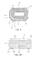
FIG. 2 is a cross-sectional view taken along line A-A' inFIG. 1 ; -
FIG. 3 is a cross-sectional view taken along line B-B' inFIG. 1 ; -
FIGS. 4A through 4F are plan views illustrating substrates of the inductor according to various modification embodiments of the present invention; -
FIG. 5 is a plan cross-sectional view illustrating a structure of a magnetic module for a power inductor according to another embodiment of the present invention; -
FIG. 6 is a plan cross-sectional view illustrating only a substrate in the structure ofFIG. 5 ; and -
FIG. 7 is a graph showing a comparison of inductance and series resistance between the inductor according to the embodiment of the present invention and an inductor according to the related art. - Hereinafter, embodiments of the present invention will be described in detail with reference to the accompanying drawings. The invention may, however, be embodied in many different forms and should not be construed as being limited to the embodiments set forth herein. Rather, these embodiments are provided so that this disclosure will be thorough and complete, and will fully convey the scope of the invention to those skilled in the art. In the drawings, the shapes and dimensions of elements may be exaggerated for clarity, and the same reference numerals will be used throughout to designate the same or like elements.
- Referring to
FIGS. 1 through 3 , aninductor 1 according to an embodiment of the present invention includes amain body 10 and first and secondexternal electrodes main body 10. - In the following description, it will be defined that an "L direction" is a "length direction", a "W direction" is a "width direction", and a "T direction" is a "thickness direction" following directions of
FIG. 1 . - The
main body 10 may have a rectangular parallelepiped shape and include upper andlower cover layers coil support layer 30 disposed between the upper andlower cover layers second coil layers coil support layer 30 and having respective one ends electrically connected to the first and secondexternal electrodes - The upper and
lower cover layers - The upper and
lower cover layers second coil layers - The first and second
external electrodes external electrodes - Here, a nickel-plated layer (not shown) or a tin-plated layer (not shown) may be further formed on a surface of the first and second
external electrodes - The
coil support layer 30 may be fabricated as a substrate formed of, for example, an electrically insulating material such as a photosensitive polymer, or a magnetic material such as ferrite, or the like. - Also, a photosensitive insulating material may be interposed between the first and
second coil layers second coil layers - The conductive via may be formed by forming a through hole (not shown) penetrating the
coil support layer 30 in a thickness direction, and filling the through hole with a conductive paste, or the like. - In order to increase inductance, the number of turns of the first and
second coil layers second coil layers - However, in order to increase inductance by an amount equal to the increased number of turns of the first and second coil layers 41 and 42, a certain size of the through
hole 63 of the coil support layers 30 should be secured, so that there is a limitation in increasing the number of turns of the first and second coil layers 41 and 42. - Also, in the case in which a thickness of the first and second coil layers 41 and 42 is reduced to increase the number of turns of the first and second coil layers 41 and 42, resistance may be increased.
- Meanwhile, in the case in which the length of the first and second coil layers 41 and 42 is increased, resistance may be increased in proportion thereto.
- Thus, in the present embodiment, a structure of decreasing the length of the first and second coil layers 41 and 42 to reduce resistance, while maintaining inductance at a certain level, may be suggested as follows.
- In the
coil support layer 30, the throughhole 63 may be formed in the center of thecoil support layer 30,first recess portions 61 may be formed in both lateral surfaces thereof in the length direction, and a plurality ofsecond recess portions 62 may be formed in respective corners thereof. - The
coil support layer 30 has magnetic permeability lower than that of a magnetic material of themain body 10, and thus, magnetic flux may not be circulate smoothly to thereby lower inductance. - However, in the present embodiment, magnetic flux can be circulate smoothly through the through
hole 63 and the first andsecond recess portions - Table 1 below shows inductance changes over area ratios of the through
hole 63 to thesecond recess portions 62. Here, an inductance change rate (%) denotes a ratio by which inductance values of sample 2 to sample 7 are decreased with respect to an inductance value ofsample 1.[Table 1] Area of through hole Area of second recess portions Area ratio of through hole/second recess portions Inductance (uH) Inductance change rate (%) Sample 10.902655 0.899 0.99 1.05 0 Sample 2 0.902655 0.811 0.90 1.02 3 Sample 3 0.902655 0.724 0.80 0.98 6 Sample 4 0.902655 0.636 0.70 0.92 12 Sample 5 0.902655 0.541 0.60 0.88 16 Sample 6 0.902655 0.454 0.50 0.62 41 Sample 7 0.902655 0.363 0.40 0.41 61 - Referring to Table 1, it can be seen that when an area of the through hole is fixed to 0.902655, inductance may be changed according to an area ratio of the through
hole 63 to thesecond recess portions 62. - In particular, in the case of sample 6 and sample 7 in which the area ratio of the through
hole 63 to thesecond recess portions 62 is reduced to 50% or below, inductance is rapidly lowered from 0.88 in sample 5 to 0.62 and from 0.62 in sample 6 to 0.41. Also, the inductance change rate is sharply reduced from 16% in sample 5 to 41% and from 41% in sample 6 to 61%, and thus, it can be confirmed that the ratio of the throughhole 63 to thesecond recess portions 62 needs to be 60% (0.60) or greater in order to maintain a certain inductance value. - The first and second coil layers 41 and 42 of the
coil support layer 30 have a substantially helical structure and may have a polygonal shape such as a quadrangular shape, a pentagonal shape, a hexagonal shape, a circular shape, an oval shape, or the like. Also, the first and second coil layers 41 and 42 of thecoil support layer 30 may have an irregular shape as necessary. - As illustrated in
FIGS. 1 through 3 , when themain body 10 is a rectangular parallelepiped, the first and second coil layers 41 and 42 may have a quadrangular shape to allow for the area of the first and second coil layers 41 and 42 to be significantly increased, such that a strength of an induced magnetic field may be significantly increased. - Respective one ends of the first and second coil layers 41 and 42 are led out to end portions of the
coil support layer 30 so as to be electrically connected to the first and secondexternal electrodes - Also, the respective other ends of the first and second coil layers 41 and 42 may be positioned in the vicinity of the center of the
coil support layer 30 so as to be electrically connected through a via conductor (not shown). - The first and second coil layers 41 and 42 may have magnetic permeability of 80% or below and may include at least one metal selected from the group consisting of gold (Au), silver (Ag), platinum (Pt), copper (Cu), nickel (Ni), palladium (Pd), and alloys thereof. The first and second coil layers 41 and 42 may be formed of any material, as long as the material may provide conductivity. Thus, the material of the first and second coil layers 41 and 42 is not limited to the listed metals.
- Meanwhile, in order to insulate the first and second coil layers 41 and 42 and the
main body 10, an insulatinglayer 50 may be formed on the circumference of the first and second coil layers 41 and 42 so as to cover surfaces of the first and second coil layers 41 and 42. - The insulating
layer 50 is formed of a material having insulating characteristics. For example, the insulatinglayer 50 may be formed of a polymer, or the like, but the present invention is not particularly limited thereto. - Meanwhile, the first and
second recess portions coil support layer 30 may be variably modified as necessary. -
FIGS. 4A through 4F illustrate portions of modifications of the first andsecond recess portions hole 63 of thecoil support layer 30 is not illustrated for the purpose of description. - Referring to
FIG. 4A ,first recess portions 601 andsecond recess portions 602 may be space apart from each other by two pairs of first extendingportions 302 led out to both surfaces of thecoil support layer 300 and second extendingportions 301 led out to both end portions of thecoil support layer 300. - Here, each of the
first recess portions 601 may be formed as a single elongated recess formed in the length direction of thecoil support layer 300 by two first extendingportions 302. Aninner corner surface 304 of thefirst recess portion 601 may be formed as a right angle surface, but the present invention is not limited thereto. - Also, the
second recess portions 602 may be formed in a chamfered manner on four corners of thecoil support layer 300, andinner surfaces 303 thereof may be formed as curved surfaces, but the present invention is not limited thereto and theinner surfaces 303 of thesecond recess portions 602 may be formed as flat surfaces when necessary. - Referring to
FIG. 4B ,first recess portions 611 andsecond recess portions 612 may be space apart from each other by two pairs of first extendingportions 312 led out to both lateral surfaces of acoil support layer 310 and second extendingportions 311 led out to both end portions of thecoil support layer 310. - Here, each of the
first recess portions 611 may be formed as a single elongated recess formed in the length direction of thecoil support layer 310 by the two first extendingportions 312. Aninner corner surface 314 of thefirst recess portion 611 may be formed as a curved surface, but the present invention is not limited thereto. - Also, the
second recess portions 612 may be formed in a chamfered manner on four corners of thecoil support layer 310, andinner surfaces 313 thereof may be formed as curved surfaces, but the present invention is not limited thereto and theinner surfaces 313 of thesecond recess portions 612 may be formed as flat surfaces when necessary. - Referring to
FIG. 4C ,first recess portions 621 andsecond recess portions 622 may be space apart from each other by a pair of first extendingportions 322 led out to both lateral surfaces of acoil support layer 320 and second extendingportions 321 led out to both end portions of thecoil support layer 320. - Here, the
first recess portions 621 may be two recesses spaced apart from each other in the length direction of thecoil support layer 320 by the first extendingportion 322. Thefirst recess portion 621 and thesecond reception portion 622, adjacent to each other and divided by the second extendingportion 321 may be formed to communicate with each other, but the present invention is not limited thereto. - Also,
inner surfaces 323 of thesecond recess portions 622 may be formed as curved surfaces, but the present invention is not limited thereto and theinner surfaces 323 of thesecond recess portions 622 may be formed as flat surfaces when necessary. - Referring to
FIG. 4D ,first recess portions 631 andsecond recess portions 632 may be spaced apart from each other by a plurality of first extendingportions 332 led out to both lateral surfaces of acoil support layer 330 and second extendingportions 331 led out to both end portions of thecoil support layer 330. - Here, the
first recess portions 631 may be a plurality of recesses spaced apart from each other in the length direction of thecoil support layer 330 by the plurality of first extendingportions 332. Aninner corner surface 334 of thefirst recess portion 631 may be formed as a right angle surface, but the present invention is not limited thereto. - Also, the
second recess portions 632 may be formed in a chamfered manner on four corners of thecoil support layer 330, andinner surfaces 333 thereof may be formed as curved surfaces, but the present invention is not limited thereto and theinner surfaces 333 of thesecond recess portions 632 may be formed as flat surfaces when necessary. - Referring to
FIG. 4E ,first recess portions 641 andsecond recess portions 642 may be spaced apart from each other by two pairs of first extendingportions 342a led out to both lateral surfaces of acoil support layer 340 and second extendingportions 341 led out to both end portions of thecoil support layer 340. - Here, an
inner corner surface 344 of thefirst recess portion 641 may be formed as a curved surface, but the present invention is not limited thereto. - Also, the
second recess portions 642 may be formed in a chamfered manner on four corners of thecoil support layer 340, andinner surfaces 343 thereof may be formed as curved surfaces, but the present invention is not limited thereto and theinner surfaces 343 of thesecond recess portions 642 may be formed as flat surfaces when necessary. - Referring to
FIG. 4F ,first recess portions 651 andsecond recess portions 652 may be spaced apart from each other by a plurality of first extendingportions 352 led out to both lateral surfaces of acoil support layer 350 and second extendingportions 351 led out to both end portions of thecoil support layer 350. - Here, the
first recess portions 651 may be a plurality of recesses spaced apart from each other in the length direction of thecoil support layer 350 by the plurality of first extendingportions 352, and aninner surface 354 of thefirst recess portion 651 may be formed as a curved surface, but the present invention is not limited thereto. - Also, the
second recess portions 652 may be formed on four corners of thecoil support layer 350 in a chamfered manner, andinner surfaces 353 thereof may be formed as curved surfaces, but the present invention is not limited thereto and theinner surfaces 353 of thesecond recess portions 652 may be formed as flat surfaces when necessary. -
FIGS. 5 and6 illustrate amagnetic module 100 for a power inductor in which a plurality ofmain bodies 10 are connected with each other in a matrix form before the first and secondexternal electrodes main body 10 in thepower inductor 1 configured as described above. - Here,
reference numeral 70 denotes a cutting line for cutting themagnetic module 100 into magnetic body units for manufacturing respective power inductors. -
FIG. 7 is a graph showing a comparison of inductance and series resistance between the inductor according to the embodiment of the present invention and an inductor according to the related art. - Referring to
FIG. 7 , an inductor according to the embodiment of the present invention (hereinafter referred to as an inventive example) which includes a recess for a magnetic flux circulation has inductance of 0.95 uH while an inductor according to the related art (hereinafter referred to as an related art example), without a recess for a magnetic flux circulation has inductance of 0.94 uH, and accordingly inductance of the inventive example is smaller than that of the related art example by about 1 %. - Also, series resistance of the inventive example is 231.1mΩ and that of the related art example is 198.8 mΩ, so it can be seen that series resistance of the inventive example of the present invention is greater than that of the related art example by about 14%.
- In general, inductance is increased in proportion to the number of turns of a coil and a length of the coil, and series resistance is also increased in proportion to the number of turns of a coil and a length of the coil.
- In case of the power inductor, it is necessary to maintain series resistance at as low a level as possible while satisfying a required inductance value, but in case of a large inductor, a coil may have a large thickness, eliminating degradation in product characteristics due to an increase in series resistance.
- However, when the size of an inductor is reduced according to the tendency toward a reduction in size of products, there is limitations in increasing a thickness of a coil, and thus, series resistance is increased to degrade product characteristics.
- In the embodiment, it can be seen that series resistance can be significantly lowered while a similar level of inductance is maintained owing to the through
hole 63 and the first andsecond recess portions coil support layer 30, in comparison to a thin film type power inductor according to the related art. - Thus, in the present embodiment, a product in which a size of a coil layer is increased to meet the requirements of inductance while reducing series resistance, even in the case that a size of the product is small.
- Hereinafter, a method of manufacturing a power inductor according to an embodiment of the present invention will be described.
- First, a substrate formed of an insulating material or a magnetic material is prepared. Here, the substrate refers to the coil support layer, and thus, it will be denoted by the
same reference numeral 30. - The
substrate 30 includes the throughhole 63 in the center thereof, and at least onefirst recess portion 61 formed in both lateral surfaces thereof, and a plurality ofsecond recess portions 62 formed in respective corners thereof to allow magnetic flux to circulate smoothly. - Here, the
first recess portion 61 may be formed as an elongated recess in the length direction of thesubstrate 30 or may be formed as a plurality of separated recesses by cutting some portions of both lateral surfaces of thesubstrate 30 while leaving other portions thereof. Also, thefirst recess portion 61 and thesecond recess portion 62 may be in communication with each other as necessary. - Next, the first and second coil layers 41 and 42 are formed on both surfaces of the
substrate 30. - The first and second coil layers 41 and 42 may be formed in the following order. That is, a conductive paste may be applied to one surface of the
substrate 30 to form thefirst coil layer 41, a conductive via penetrating thesubstrate 30 is formed, and a conductive paste is applied to a surface opposite to the surface on which thefirst coil layer 41 is formed, to form thesecond coil layer 42. The first and second coil layers 41 and 42 may be electrically connected through the conductive via. - The conductive via may be formed by forming a through hole in the thickness direction of the
substrate 30 by using a laser, a punching machine, or the like, and filling the through hole with a conductive paste, or the like. - Here, the conductive paste may include a metal able to provide electrical conductivity. For example, the conductive paste may include at least one metal selected from the group consisting of gold (Au), silver (Ag), platinum (Pt), copper (Cu), nickel (Ni), palladium (Pd), and alloys thereof.
- Also, the first and second coil layers 41 and 42 and the conductive via may be formed of the same material in order to obtain stable electrical characteristics.
- Thereafter, the
substrate 30 having the first and second coil layers 41 and 42 formed thereon is disposed on thelower cover layer 12 formed of a magnetic material. - Here, a plurality of
substrates 30 may be laminated in the thickness direction of themain body 10, and one end portions of the first orsecond coil layer substrates 30, adjacent in the lamination direction, may be in contact with each other through a via conductor (not shown) so as to be electrically connected. - Also, an insulating layer may be formed of a material such as a polymer having insulating characteristics, or the like, to cover surfaces of the first and second coil layers 41 and 42 along the circumference thereof.
- Thereafter, the
upper cover layer 11 formed of a composite of ferrite or a metallic magnetic power and a polymer is formed on thesubstrate 30 having thefirst coil layer 41 formed thereon to manufacture themain body 10. - The
upper cover layer 11 may be formed on thesubstrate 30 by further laminating a cover sheet formed of a material including a composite of ferrite or metallic magnetic powder and a polymer, or by casting a paste formed of the same material. - Thereafter, the first and second
external electrodes main body 10 such that they are electrically connected to the portions of the first and second coil layers 41 and 42 led thereto. - Here, the first and second
external electrodes main body 10 in a conductive paste, a method of printing, depositing, or sputtering a conductive paste onto both end portions of themain body 10, or the like. - The conductive paste may be formed of a metal that may be able to provide electrical conductivity to the first and second
external electrodes - A nickel-plated layer or a tin-plated layer may further be formed on the surfaces of the first and second
external electrodes - As set forth above, according to embodiments of the invention, recesses for a magnetic flux circulation are formed in the center, both lateral surfaces, and respective corners of the coil support layers, whereby the power inductor having a low series resistance, while implementing high inductance characteristics, can be realized even in the case that the power inductor is small, and a manufacturing method thereof can also be realized.
- While the present invention has been shown and described in connection with the embodiments, it will be apparent to those skilled in the art that modifications and variations can be made without departing from the spirit and scope of the invention as defined by the appended claims.
Claims (17)
- A power inductor comprising:a main body; andfirst and second external electrodes formed on both end portions of the main body,wherein the main body includes: upper and lower cover layers; at least one coil support layer having a through hole formed in a center thereof, at least one first recess portion formed in both lateral surfaces thereof and a plurality of second recess portions formed in respective corners thereof, and disposed between the upper and lower cover layers; and first and second coil layers formed on both surfaces of the coil support layer and having respective one ends thereof connected to the first and second external electrodes.
- The power inductor of claim 1, wherein the coil support layer has magnetic permeability of 80% or below.
- The power inductor of claim 1, wherein an area ratio of the through hole to all of the second recess portions in the coil support layer is 0.60 or greater.
- The power inductor of claim 1, wherein the first recess portion of the coil support layer is formed as an elongated recess in a length direction of the coil support layer.
- The power inductor of claim 1, wherein the first recess portion of the coil support layer includes a plurality of recess portions spaced apart from each other in a length direction of the coil support layer.
- The power inductor of claim 1, wherein the first recess portion of the coil support layer is formed to communicate with the second recess portions of the coil support layer.
- The power inductor of claim 1, wherein the coil support layer is a substrate formed of an insulating material or a magnetic material.
- The power inductor of claim 1, wherein an insulating layer is formed on a circumference of the first and second coil layers.
- A magnetic module for a power inductor, including main bodies connected in a matrix form,
wherein each of the main bodies includes:upper and lower cover layers;at least one coil support layer having a central through hole provided therein, at least one first recess portion formed in both lateral surfaces thereof and a plurality of second recess portions formed in respective corners thereof, and disposed between the upper and lower cover layers; andfirst and second coil layers formed on both surfaces of the coil support layer and having respective one ends exposed to the outside. - The magnetic module for a power inductor of claim 9, wherein the coil support layer has magnetic permeability of 80% or below.
- The magnetic module for a power inductor of claim 9, wherein an area ratio of the through hole to all of the second recess portions in the coil support layer is 0.60 or greater.
- A method of manufacturing a power inductor, the method comprising:preparing a substrate formed of an insulating material or a magnetic material and having a through hole in a center thereof, at least one first recess portion formed in both lateral surfaces thereof, and a plurality of second recess portions formed in respective corners thereof;forming first and second coil layers on both surfaces of the substrate;disposing the substrate having the first and second coil layers formed thereon, on a lower cover layer;forming a main body by forming an upper cover layer on the substrate; andforming first and second external electrodes on both end portions of the main body such that the first and second external electrodes are connected to portions of the first and second coil layers led thereto.
- The method of claim 12, wherein before the disposing of the substrate, covering a circumference of the substrate having the first and second coil layers formed thereon, with an insulating material, is performed.
- The method of claim 12, wherein the disposing of the substrate includes laminating a plurality of substrates on the lower cover layer.
- The method of claim 12, wherein in the preparing of the substrate, the first recess portion is formed as an elongated recess in a length direction of the coil support layer.
- The method of claim 12, wherein in the preparing of the substrate, both lateral surfaces of the substrate are removed to leave only portions thereof to form a plurality of first recess portions spaced apart from each other.
- The method of claim 12, wherein in the preparing of the substrate, the first recess portion is formed to communicate with the second recess portions.
Applications Claiming Priority (1)
| Application Number | Priority Date | Filing Date | Title |
|---|---|---|---|
| KR1020120078421A KR20140011693A (en) | 2012-07-18 | 2012-07-18 | Magnetic substance module for power inductor, power inductor and manufacturing method for the same |
Publications (2)
| Publication Number | Publication Date |
|---|---|
| EP2688074A1 true EP2688074A1 (en) | 2014-01-22 |
| EP2688074B1 EP2688074B1 (en) | 2018-08-01 |
Family
ID=48013888
Family Applications (1)
| Application Number | Title | Priority Date | Filing Date |
|---|---|---|---|
| EP13275063.9A Not-in-force EP2688074B1 (en) | 2012-07-18 | 2013-03-14 | Magnetic module for power inductor, power inductor, and manufacturing method thereof |
Country Status (5)
| Country | Link |
|---|---|
| US (1) | US9478334B2 (en) |
| EP (1) | EP2688074B1 (en) |
| JP (1) | JP6455959B2 (en) |
| KR (1) | KR20140011693A (en) |
| CN (1) | CN103578708B (en) |
Cited By (1)
| Publication number | Priority date | Publication date | Assignee | Title |
|---|---|---|---|---|
| CN105931813A (en) * | 2016-06-28 | 2016-09-07 | 浙江科升电力设备有限公司 | Energy-saving exciting diversion iron-core reactor |
Families Citing this family (46)
| Publication number | Priority date | Publication date | Assignee | Title |
|---|---|---|---|---|
| US9001527B2 (en) * | 2008-02-18 | 2015-04-07 | Cyntec Co., Ltd. | Electronic package structure |
| JP5965148B2 (en) * | 2012-01-05 | 2016-08-03 | 日東電工株式会社 | Power receiving module for mobile terminal using wireless power transmission and rechargeable battery for mobile terminal equipped with power receiving module for mobile terminal |
| KR102004783B1 (en) * | 2014-02-04 | 2019-07-29 | 삼성전기주식회사 | Composite electronic component and board for mounting the same |
| KR101823191B1 (en) * | 2014-05-07 | 2018-01-29 | 삼성전기주식회사 | Chip electronic component and manufacturing method thereof |
| KR102186153B1 (en) * | 2014-05-23 | 2020-12-03 | 삼성전기주식회사 | Chip electronic component and manufacturing method thereof |
| KR101532171B1 (en) * | 2014-06-02 | 2015-07-06 | 삼성전기주식회사 | Inductor and Manufacturing Method for the Same |
| KR101686989B1 (en) * | 2014-08-07 | 2016-12-19 | 주식회사 모다이노칩 | Power inductor |
| KR101662206B1 (en) | 2014-08-07 | 2016-10-06 | 주식회사 모다이노칩 | Power inductor |
| KR101681201B1 (en) | 2014-09-11 | 2016-12-01 | 주식회사 모다이노칩 | Power inductor |
| JP6331953B2 (en) | 2014-10-15 | 2018-05-30 | 株式会社村田製作所 | Electronic components |
| KR101832547B1 (en) | 2014-12-12 | 2018-02-26 | 삼성전기주식회사 | Chip electronic component and manufacturing method thereof |
| KR102105394B1 (en) * | 2015-03-09 | 2020-04-28 | 삼성전기주식회사 | Coil component and and board for mounting the same |
| US10951123B2 (en) | 2015-04-23 | 2021-03-16 | Chicony Power Technology Co.. Ltd. | Power conversion system |
| US9559609B2 (en) | 2015-04-23 | 2017-01-31 | Chicony Power Technology Co., Ltd. | Integrated power-converting module |
| US10395810B2 (en) | 2015-05-19 | 2019-08-27 | Shinko Electric Industries Co., Ltd. | Inductor |
| KR102171676B1 (en) * | 2015-05-26 | 2020-10-29 | 삼성전기주식회사 | Chip electronic component |
| KR101832560B1 (en) | 2015-08-07 | 2018-02-26 | 삼성전기주식회사 | Coil electronic component and method for manufacturing same |
| KR101762023B1 (en) * | 2015-11-19 | 2017-08-04 | 삼성전기주식회사 | Coil component and and board for mounting the same |
| WO2017090950A1 (en) * | 2015-11-24 | 2017-06-01 | 주식회사 모다이노칩 | Power inductor |
| KR101900880B1 (en) * | 2015-11-24 | 2018-09-21 | 주식회사 모다이노칩 | Power Inductor |
| KR101762039B1 (en) | 2015-12-18 | 2017-07-26 | 삼성전기주식회사 | Coil component |
| CN105551780A (en) * | 2016-01-28 | 2016-05-04 | 深圳市麦捷微电子科技股份有限公司 | High-performance side-welding winding power inductor |
| KR102419961B1 (en) * | 2016-02-18 | 2022-07-13 | 삼성전기주식회사 | Inductor |
| KR101862465B1 (en) * | 2016-08-09 | 2018-05-29 | 삼성전기주식회사 | Coil component |
| KR101981466B1 (en) | 2016-09-08 | 2019-05-24 | 주식회사 모다이노칩 | Power Inductor |
| WO2018048135A1 (en) * | 2016-09-08 | 2018-03-15 | 주식회사 모다이노칩 | Power inductor |
| JP6400803B2 (en) * | 2016-10-28 | 2018-10-03 | サムソン エレクトロ−メカニックス カンパニーリミテッド. | Coil parts |
| KR101942730B1 (en) * | 2017-02-20 | 2019-01-28 | 삼성전기 주식회사 | Coil electronic component |
| KR102369430B1 (en) | 2017-03-15 | 2022-03-03 | 삼성전기주식회사 | Coil electronic component and board having the same |
| JP7073650B2 (en) * | 2017-08-25 | 2022-05-24 | Tdk株式会社 | Coil parts |
| KR102016494B1 (en) * | 2017-10-23 | 2019-09-02 | 삼성전기주식회사 | Coil component |
| KR20190087829A (en) * | 2018-01-17 | 2019-07-25 | 삼성전기주식회사 | Coil component and manufacturing method for the same |
| JP6962284B2 (en) * | 2018-07-17 | 2021-11-05 | 株式会社村田製作所 | Inductor parts |
| JP7070188B2 (en) * | 2018-07-17 | 2022-05-18 | 株式会社村田製作所 | Inductor parts |
| KR102080650B1 (en) | 2018-09-21 | 2020-02-24 | 삼성전기주식회사 | Coil component and manufacturing method for the same |
| KR102148832B1 (en) | 2018-10-12 | 2020-08-27 | 삼성전기주식회사 | Coil component |
| KR102430635B1 (en) | 2018-10-12 | 2022-08-09 | 삼성전기주식회사 | Coil component |
| KR102678629B1 (en) * | 2018-10-31 | 2024-06-27 | 삼성전기주식회사 | Coil component and manufacturing method of coil component |
| KR102145308B1 (en) * | 2019-03-06 | 2020-08-18 | 삼성전기주식회사 | Coil component and manufacturing method for the same |
| JP7143817B2 (en) * | 2019-05-24 | 2022-09-29 | 株式会社村田製作所 | Laminated coil parts |
| KR102198533B1 (en) | 2019-05-27 | 2021-01-06 | 삼성전기주식회사 | Coil component |
| KR102679990B1 (en) * | 2019-07-17 | 2024-07-02 | 삼성전기주식회사 | Coil component |
| CN114586117B (en) * | 2019-11-26 | 2025-10-28 | 华为技术有限公司 | Inductor and manufacturing method thereof, voltage conversion circuit and electronic equipment |
| KR102827665B1 (en) * | 2020-05-18 | 2025-07-02 | 삼성전기주식회사 | Coil component |
| KR102747222B1 (en) * | 2020-05-21 | 2024-12-31 | 삼성전기주식회사 | Coil component |
| KR102899088B1 (en) * | 2020-11-26 | 2025-12-11 | 삼성전기주식회사 | Coil component |
Citations (7)
| Publication number | Priority date | Publication date | Assignee | Title |
|---|---|---|---|---|
| WO1998054733A2 (en) * | 1997-05-29 | 1998-12-03 | Tdk Corporation Of America | Low profile pin-less planar magnetic devices and method of making same |
| EP1103993A1 (en) * | 1999-11-26 | 2001-05-30 | Taiyo Yuden Co., Ltd. | Surface-mount coil and method for manufacturing same |
| US20040263309A1 (en) * | 2003-02-26 | 2004-12-30 | Tdk Corporation | Thin-film type common-mode choke coil and manufacturing method thereof |
| US20060068602A1 (en) * | 2004-09-30 | 2006-03-30 | Tdk Corporation | Electronic device having organic material based insulating layer and method for fabricating the same |
| US20060077029A1 (en) * | 2004-10-07 | 2006-04-13 | Freescale Semiconductor, Inc. | Apparatus and method for constructions of stacked inductive components |
| EP1965396A1 (en) * | 2005-12-07 | 2008-09-03 | Sumida Corporation | Flexible coil |
| US20100231344A1 (en) * | 2009-03-11 | 2010-09-16 | Shinko Electric Industries Co., Ltd. | Inductor device, and method of manufacturing the same |
Family Cites Families (17)
| Publication number | Priority date | Publication date | Assignee | Title |
|---|---|---|---|---|
| JPH1154327A (en) * | 1997-08-04 | 1999-02-26 | Murata Mfg Co Ltd | Coil parts |
| KR100249211B1 (en) | 1997-11-26 | 2000-03-15 | 구자홍 | Method of manufacturing thin film inductor |
| JP3827311B2 (en) | 2003-02-26 | 2006-09-27 | Tdk株式会社 | Manufacturing method of common mode choke coil |
| CN1817070A (en) | 2003-07-03 | 2006-08-09 | 皇家飞利浦电子股份有限公司 | Soft magnetic materials for the manufacture of printed circuit boards |
| JPWO2005122192A1 (en) * | 2004-06-07 | 2008-04-10 | 株式会社村田製作所 | Laminated coil |
| KR100770249B1 (en) * | 2004-06-07 | 2007-10-25 | 가부시키가이샤 무라타 세이사쿠쇼 | Laminated coil |
| KR100631893B1 (en) | 2004-12-02 | 2006-10-09 | 삼성전기주식회사 | Planar magnetic inductor and manufacturing method thereof |
| JP4638322B2 (en) * | 2005-10-25 | 2011-02-23 | Tdk株式会社 | Common mode filter |
| US7791445B2 (en) | 2006-09-12 | 2010-09-07 | Cooper Technologies Company | Low profile layered coil and cores for magnetic components |
| KR101174541B1 (en) | 2007-02-02 | 2012-08-16 | 가부시키가이샤 무라타 세이사쿠쇼 | laminated coil component |
| JP5054445B2 (en) * | 2007-06-26 | 2012-10-24 | スミダコーポレーション株式会社 | Coil parts |
| TWM357691U (en) * | 2008-11-07 | 2009-05-21 | Delta Electronics Inc | Transformer |
| US7843303B2 (en) * | 2008-12-08 | 2010-11-30 | Alpha And Omega Semiconductor Incorporated | Multilayer inductor |
| US8232855B2 (en) * | 2008-12-15 | 2012-07-31 | General Electric Company | High energy density inductor |
| JP2010205905A (en) * | 2009-03-03 | 2010-09-16 | Fuji Electric Systems Co Ltd | Magnetic component, and method of manufacturing the magnetic component |
| KR101434351B1 (en) * | 2010-10-21 | 2014-08-26 | 티디케이가부시기가이샤 | Coil component and method for producing same |
| US9009951B2 (en) * | 2012-04-24 | 2015-04-21 | Cyntec Co., Ltd. | Method of fabricating an electromagnetic component |
-
2012
- 2012-07-18 KR KR1020120078421A patent/KR20140011693A/en not_active Ceased
-
2013
- 2013-03-14 EP EP13275063.9A patent/EP2688074B1/en not_active Not-in-force
- 2013-03-14 JP JP2013051347A patent/JP6455959B2/en active Active
- 2013-03-15 US US13/839,607 patent/US9478334B2/en active Active
- 2013-03-28 CN CN201310104695.3A patent/CN103578708B/en active Active
Patent Citations (7)
| Publication number | Priority date | Publication date | Assignee | Title |
|---|---|---|---|---|
| WO1998054733A2 (en) * | 1997-05-29 | 1998-12-03 | Tdk Corporation Of America | Low profile pin-less planar magnetic devices and method of making same |
| EP1103993A1 (en) * | 1999-11-26 | 2001-05-30 | Taiyo Yuden Co., Ltd. | Surface-mount coil and method for manufacturing same |
| US20040263309A1 (en) * | 2003-02-26 | 2004-12-30 | Tdk Corporation | Thin-film type common-mode choke coil and manufacturing method thereof |
| US20060068602A1 (en) * | 2004-09-30 | 2006-03-30 | Tdk Corporation | Electronic device having organic material based insulating layer and method for fabricating the same |
| US20060077029A1 (en) * | 2004-10-07 | 2006-04-13 | Freescale Semiconductor, Inc. | Apparatus and method for constructions of stacked inductive components |
| EP1965396A1 (en) * | 2005-12-07 | 2008-09-03 | Sumida Corporation | Flexible coil |
| US20100231344A1 (en) * | 2009-03-11 | 2010-09-16 | Shinko Electric Industries Co., Ltd. | Inductor device, and method of manufacturing the same |
Cited By (1)
| Publication number | Priority date | Publication date | Assignee | Title |
|---|---|---|---|---|
| CN105931813A (en) * | 2016-06-28 | 2016-09-07 | 浙江科升电力设备有限公司 | Energy-saving exciting diversion iron-core reactor |
Also Published As
| Publication number | Publication date |
|---|---|
| EP2688074B1 (en) | 2018-08-01 |
| US9478334B2 (en) | 2016-10-25 |
| JP2014022724A (en) | 2014-02-03 |
| US20140022041A1 (en) | 2014-01-23 |
| CN103578708A (en) | 2014-02-12 |
| CN103578708B (en) | 2018-03-13 |
| JP6455959B2 (en) | 2019-01-23 |
| KR20140011693A (en) | 2014-01-29 |
Similar Documents
| Publication | Publication Date | Title |
|---|---|---|
| EP2688074B1 (en) | Magnetic module for power inductor, power inductor, and manufacturing method thereof | |
| US9343228B2 (en) | Laminated inductor and manufacturing method thereof | |
| KR101792281B1 (en) | Power Inductor and Manufacturing Method for the Same | |
| KR101670184B1 (en) | Multilayered electronic component and manufacturing method thereof | |
| US9251943B2 (en) | Multilayer type inductor and method of manufacturing the same | |
| KR20170032057A (en) | Multilayered electronic component | |
| KR20170045629A (en) | Multilayered electronic component and manufacturing method thereof | |
| KR20140003056A (en) | Power inductor and manufacturing method of the same | |
| KR20150058869A (en) | Multi-layered inductor | |
| KR20140011694A (en) | Chip device, multi-layered chip device and method of producing the same | |
| US9287031B2 (en) | Multilayer inductor and method of manufacturing the same | |
| US20130321115A1 (en) | Multilayered-type inductor and method of manufacturing the same | |
| KR20150114799A (en) | Multilayered array electronic component and manufacturing method thereof | |
| KR101153496B1 (en) | A layered inductor and a manufacturing method thereof | |
| KR20150089211A (en) | Chip-type Coil Component | |
| KR102004815B1 (en) | Magnetic Substance Module for Power Inductor, Power Inductor and Manufacturing Method for the Same | |
| KR101963267B1 (en) | Multi-layered inductor and board for mounting the same | |
| KR20160100017A (en) | Method for manufacturing inductor device | |
| KR101994724B1 (en) | Laminated Inductor and Manufacturing Method Thereof | |
| KR20120045949A (en) | A layered inductor and a manufacturing method thereof | |
| KR20170032017A (en) | Multilayered inductor | |
| KR20140015074A (en) | Power inductor | |
| KR20150018206A (en) | Laminated Inductor | |
| KR101946260B1 (en) | Multilayered electronic component array and manufacturing method thereof | |
| KR20140141170A (en) | Multi-layered inductor |
Legal Events
| Date | Code | Title | Description |
|---|---|---|---|
| PUAI | Public reference made under article 153(3) epc to a published international application that has entered the european phase |
Free format text: ORIGINAL CODE: 0009012 |
|
| AK | Designated contracting states |
Kind code of ref document: A1 Designated state(s): AL AT BE BG CH CY CZ DE DK EE ES FI FR GB GR HR HU IE IS IT LI LT LU LV MC MK MT NL NO PL PT RO RS SE SI SK SM TR |
|
| AX | Request for extension of the european patent |
Extension state: BA ME |
|
| 17P | Request for examination filed |
Effective date: 20140715 |
|
| RAP1 | Party data changed (applicant data changed or rights of an application transferred) |
Owner name: SAMSUNG ELECTRO-MECHANICS CO., LTD. |
|
| GRAP | Despatch of communication of intention to grant a patent |
Free format text: ORIGINAL CODE: EPIDOSNIGR1 |
|
| STAA | Information on the status of an ep patent application or granted ep patent |
Free format text: STATUS: GRANT OF PATENT IS INTENDED |
|
| INTG | Intention to grant announced |
Effective date: 20180301 |
|
| GRAS | Grant fee paid |
Free format text: ORIGINAL CODE: EPIDOSNIGR3 |
|
| GRAA | (expected) grant |
Free format text: ORIGINAL CODE: 0009210 |
|
| STAA | Information on the status of an ep patent application or granted ep patent |
Free format text: STATUS: THE PATENT HAS BEEN GRANTED |
|
| AK | Designated contracting states |
Kind code of ref document: B1 Designated state(s): AL AT BE BG CH CY CZ DE DK EE ES FI FR GB GR HR HU IE IS IT LI LT LU LV MC MK MT NL NO PL PT RO RS SE SI SK SM TR |
|
| REG | Reference to a national code |
Ref country code: GB Ref legal event code: FG4D |
|
| REG | Reference to a national code |
Ref country code: CH Ref legal event code: EP Ref country code: AT Ref legal event code: REF Ref document number: 1025288 Country of ref document: AT Kind code of ref document: T Effective date: 20180815 |
|
| REG | Reference to a national code |
Ref country code: IE Ref legal event code: FG4D |
|
| REG | Reference to a national code |
Ref country code: DE Ref legal event code: R096 Ref document number: 602013041105 Country of ref document: DE |
|
| REG | Reference to a national code |
Ref country code: NL Ref legal event code: MP Effective date: 20180801 |
|
| REG | Reference to a national code |
Ref country code: LT Ref legal event code: MG4D |
|
| REG | Reference to a national code |
Ref country code: AT Ref legal event code: MK05 Ref document number: 1025288 Country of ref document: AT Kind code of ref document: T Effective date: 20180801 |
|
| PG25 | Lapsed in a contracting state [announced via postgrant information from national office to epo] |
Ref country code: NO Free format text: LAPSE BECAUSE OF FAILURE TO SUBMIT A TRANSLATION OF THE DESCRIPTION OR TO PAY THE FEE WITHIN THE PRESCRIBED TIME-LIMIT Effective date: 20181101 Ref country code: FI Free format text: LAPSE BECAUSE OF FAILURE TO SUBMIT A TRANSLATION OF THE DESCRIPTION OR TO PAY THE FEE WITHIN THE PRESCRIBED TIME-LIMIT Effective date: 20180801 Ref country code: GR Free format text: LAPSE BECAUSE OF FAILURE TO SUBMIT A TRANSLATION OF THE DESCRIPTION OR TO PAY THE FEE WITHIN THE PRESCRIBED TIME-LIMIT Effective date: 20181102 Ref country code: SE Free format text: LAPSE BECAUSE OF FAILURE TO SUBMIT A TRANSLATION OF THE DESCRIPTION OR TO PAY THE FEE WITHIN THE PRESCRIBED TIME-LIMIT Effective date: 20180801 Ref country code: PL Free format text: LAPSE BECAUSE OF FAILURE TO SUBMIT A TRANSLATION OF THE DESCRIPTION OR TO PAY THE FEE WITHIN THE PRESCRIBED TIME-LIMIT Effective date: 20180801 Ref country code: LT Free format text: LAPSE BECAUSE OF FAILURE TO SUBMIT A TRANSLATION OF THE DESCRIPTION OR TO PAY THE FEE WITHIN THE PRESCRIBED TIME-LIMIT Effective date: 20180801 Ref country code: RS Free format text: LAPSE BECAUSE OF FAILURE TO SUBMIT A TRANSLATION OF THE DESCRIPTION OR TO PAY THE FEE WITHIN THE PRESCRIBED TIME-LIMIT Effective date: 20180801 Ref country code: AT Free format text: LAPSE BECAUSE OF FAILURE TO SUBMIT A TRANSLATION OF THE DESCRIPTION OR TO PAY THE FEE WITHIN THE PRESCRIBED TIME-LIMIT Effective date: 20180801 Ref country code: IS Free format text: LAPSE BECAUSE OF FAILURE TO SUBMIT A TRANSLATION OF THE DESCRIPTION OR TO PAY THE FEE WITHIN THE PRESCRIBED TIME-LIMIT Effective date: 20181201 Ref country code: NL Free format text: LAPSE BECAUSE OF FAILURE TO SUBMIT A TRANSLATION OF THE DESCRIPTION OR TO PAY THE FEE WITHIN THE PRESCRIBED TIME-LIMIT Effective date: 20180801 Ref country code: BG Free format text: LAPSE BECAUSE OF FAILURE TO SUBMIT A TRANSLATION OF THE DESCRIPTION OR TO PAY THE FEE WITHIN THE PRESCRIBED TIME-LIMIT Effective date: 20181101 |
|
| PG25 | Lapsed in a contracting state [announced via postgrant information from national office to epo] |
Ref country code: AL Free format text: LAPSE BECAUSE OF FAILURE TO SUBMIT A TRANSLATION OF THE DESCRIPTION OR TO PAY THE FEE WITHIN THE PRESCRIBED TIME-LIMIT Effective date: 20180801 Ref country code: LV Free format text: LAPSE BECAUSE OF FAILURE TO SUBMIT A TRANSLATION OF THE DESCRIPTION OR TO PAY THE FEE WITHIN THE PRESCRIBED TIME-LIMIT Effective date: 20180801 Ref country code: HR Free format text: LAPSE BECAUSE OF FAILURE TO SUBMIT A TRANSLATION OF THE DESCRIPTION OR TO PAY THE FEE WITHIN THE PRESCRIBED TIME-LIMIT Effective date: 20180801 |
|
| PG25 | Lapsed in a contracting state [announced via postgrant information from national office to epo] |
Ref country code: EE Free format text: LAPSE BECAUSE OF FAILURE TO SUBMIT A TRANSLATION OF THE DESCRIPTION OR TO PAY THE FEE WITHIN THE PRESCRIBED TIME-LIMIT Effective date: 20180801 Ref country code: ES Free format text: LAPSE BECAUSE OF FAILURE TO SUBMIT A TRANSLATION OF THE DESCRIPTION OR TO PAY THE FEE WITHIN THE PRESCRIBED TIME-LIMIT Effective date: 20180801 Ref country code: CZ Free format text: LAPSE BECAUSE OF FAILURE TO SUBMIT A TRANSLATION OF THE DESCRIPTION OR TO PAY THE FEE WITHIN THE PRESCRIBED TIME-LIMIT Effective date: 20180801 Ref country code: RO Free format text: LAPSE BECAUSE OF FAILURE TO SUBMIT A TRANSLATION OF THE DESCRIPTION OR TO PAY THE FEE WITHIN THE PRESCRIBED TIME-LIMIT Effective date: 20180801 Ref country code: IT Free format text: LAPSE BECAUSE OF FAILURE TO SUBMIT A TRANSLATION OF THE DESCRIPTION OR TO PAY THE FEE WITHIN THE PRESCRIBED TIME-LIMIT Effective date: 20180801 |
|
| REG | Reference to a national code |
Ref country code: DE Ref legal event code: R097 Ref document number: 602013041105 Country of ref document: DE |
|
| PG25 | Lapsed in a contracting state [announced via postgrant information from national office to epo] |
Ref country code: SM Free format text: LAPSE BECAUSE OF FAILURE TO SUBMIT A TRANSLATION OF THE DESCRIPTION OR TO PAY THE FEE WITHIN THE PRESCRIBED TIME-LIMIT Effective date: 20180801 Ref country code: DK Free format text: LAPSE BECAUSE OF FAILURE TO SUBMIT A TRANSLATION OF THE DESCRIPTION OR TO PAY THE FEE WITHIN THE PRESCRIBED TIME-LIMIT Effective date: 20180801 Ref country code: SK Free format text: LAPSE BECAUSE OF FAILURE TO SUBMIT A TRANSLATION OF THE DESCRIPTION OR TO PAY THE FEE WITHIN THE PRESCRIBED TIME-LIMIT Effective date: 20180801 |
|
| PLBE | No opposition filed within time limit |
Free format text: ORIGINAL CODE: 0009261 |
|
| STAA | Information on the status of an ep patent application or granted ep patent |
Free format text: STATUS: NO OPPOSITION FILED WITHIN TIME LIMIT |
|
| 26N | No opposition filed |
Effective date: 20190503 |
|
| PG25 | Lapsed in a contracting state [announced via postgrant information from national office to epo] |
Ref country code: SI Free format text: LAPSE BECAUSE OF FAILURE TO SUBMIT A TRANSLATION OF THE DESCRIPTION OR TO PAY THE FEE WITHIN THE PRESCRIBED TIME-LIMIT Effective date: 20180801 |
|
| PG25 | Lapsed in a contracting state [announced via postgrant information from national office to epo] |
Ref country code: MC Free format text: LAPSE BECAUSE OF FAILURE TO SUBMIT A TRANSLATION OF THE DESCRIPTION OR TO PAY THE FEE WITHIN THE PRESCRIBED TIME-LIMIT Effective date: 20180801 |
|
| REG | Reference to a national code |
Ref country code: CH Ref legal event code: PL |
|
| GBPC | Gb: european patent ceased through non-payment of renewal fee |
Effective date: 20190314 |
|
| PG25 | Lapsed in a contracting state [announced via postgrant information from national office to epo] |
Ref country code: LU Free format text: LAPSE BECAUSE OF NON-PAYMENT OF DUE FEES Effective date: 20190314 |
|
| REG | Reference to a national code |
Ref country code: BE Ref legal event code: MM Effective date: 20190331 |
|
| PG25 | Lapsed in a contracting state [announced via postgrant information from national office to epo] |
Ref country code: LI Free format text: LAPSE BECAUSE OF NON-PAYMENT OF DUE FEES Effective date: 20190331 Ref country code: CH Free format text: LAPSE BECAUSE OF NON-PAYMENT OF DUE FEES Effective date: 20190331 Ref country code: IE Free format text: LAPSE BECAUSE OF NON-PAYMENT OF DUE FEES Effective date: 20190314 Ref country code: GB Free format text: LAPSE BECAUSE OF NON-PAYMENT OF DUE FEES Effective date: 20190314 |
|
| PG25 | Lapsed in a contracting state [announced via postgrant information from national office to epo] |
Ref country code: BE Free format text: LAPSE BECAUSE OF NON-PAYMENT OF DUE FEES Effective date: 20190331 Ref country code: FR Free format text: LAPSE BECAUSE OF NON-PAYMENT OF DUE FEES Effective date: 20190331 |
|
| PG25 | Lapsed in a contracting state [announced via postgrant information from national office to epo] |
Ref country code: TR Free format text: LAPSE BECAUSE OF FAILURE TO SUBMIT A TRANSLATION OF THE DESCRIPTION OR TO PAY THE FEE WITHIN THE PRESCRIBED TIME-LIMIT Effective date: 20180801 |
|
| PG25 | Lapsed in a contracting state [announced via postgrant information from national office to epo] |
Ref country code: PT Free format text: LAPSE BECAUSE OF FAILURE TO SUBMIT A TRANSLATION OF THE DESCRIPTION OR TO PAY THE FEE WITHIN THE PRESCRIBED TIME-LIMIT Effective date: 20181201 Ref country code: MT Free format text: LAPSE BECAUSE OF NON-PAYMENT OF DUE FEES Effective date: 20190314 |
|
| PG25 | Lapsed in a contracting state [announced via postgrant information from national office to epo] |
Ref country code: CY Free format text: LAPSE BECAUSE OF FAILURE TO SUBMIT A TRANSLATION OF THE DESCRIPTION OR TO PAY THE FEE WITHIN THE PRESCRIBED TIME-LIMIT Effective date: 20180801 |
|
| PG25 | Lapsed in a contracting state [announced via postgrant information from national office to epo] |
Ref country code: HU Free format text: LAPSE BECAUSE OF FAILURE TO SUBMIT A TRANSLATION OF THE DESCRIPTION OR TO PAY THE FEE WITHIN THE PRESCRIBED TIME-LIMIT; INVALID AB INITIO Effective date: 20130314 |
|
| PGFP | Annual fee paid to national office [announced via postgrant information from national office to epo] |
Ref country code: DE Payment date: 20211206 Year of fee payment: 10 |
|
| PG25 | Lapsed in a contracting state [announced via postgrant information from national office to epo] |
Ref country code: MK Free format text: LAPSE BECAUSE OF FAILURE TO SUBMIT A TRANSLATION OF THE DESCRIPTION OR TO PAY THE FEE WITHIN THE PRESCRIBED TIME-LIMIT Effective date: 20180801 |
|
| REG | Reference to a national code |
Ref country code: DE Ref legal event code: R119 Ref document number: 602013041105 Country of ref document: DE |
|
| PG25 | Lapsed in a contracting state [announced via postgrant information from national office to epo] |
Ref country code: DE Free format text: LAPSE BECAUSE OF NON-PAYMENT OF DUE FEES Effective date: 20231003 |