EP2668721B1 - Conductive element - Google Patents
Conductive element Download PDFInfo
- Publication number
- EP2668721B1 EP2668721B1 EP12703145.8A EP12703145A EP2668721B1 EP 2668721 B1 EP2668721 B1 EP 2668721B1 EP 12703145 A EP12703145 A EP 12703145A EP 2668721 B1 EP2668721 B1 EP 2668721B1
- Authority
- EP
- European Patent Office
- Prior art keywords
- conductive
- printed article
- article according
- mesh
- tracks
- Prior art date
- Legal status (The legal status is an assumption and is not a legal conclusion. Google has not performed a legal analysis and makes no representation as to the accuracy of the status listed.)
- Active
Links
- 239000000758 substrate Substances 0.000 claims description 17
- 239000000463 material Substances 0.000 claims description 14
- OKTJSMMVPCPJKN-UHFFFAOYSA-N Carbon Chemical compound [C] OKTJSMMVPCPJKN-UHFFFAOYSA-N 0.000 claims description 7
- 229910052799 carbon Inorganic materials 0.000 claims description 7
- BQCADISMDOOEFD-UHFFFAOYSA-N Silver Chemical compound [Ag] BQCADISMDOOEFD-UHFFFAOYSA-N 0.000 claims description 6
- 229910052751 metal Inorganic materials 0.000 claims description 6
- 239000002184 metal Substances 0.000 claims description 6
- 239000004332 silver Substances 0.000 claims description 6
- 229910052709 silver Inorganic materials 0.000 claims description 6
- 239000002131 composite material Substances 0.000 claims description 4
- 239000011888 foil Substances 0.000 claims description 4
- 239000007787 solid Substances 0.000 claims description 3
- 229920000642 polymer Polymers 0.000 claims 1
- 239000000976 ink Substances 0.000 description 30
- 230000002452 interceptive effect Effects 0.000 description 10
- 238000007639 printing Methods 0.000 description 9
- 239000004020 conductor Substances 0.000 description 4
- 239000004033 plastic Substances 0.000 description 4
- 229920003023 plastic Polymers 0.000 description 4
- 239000011241 protective layer Substances 0.000 description 4
- 239000000243 solution Substances 0.000 description 4
- 230000007547 defect Effects 0.000 description 3
- 238000004519 manufacturing process Methods 0.000 description 3
- 238000000034 method Methods 0.000 description 3
- 239000000123 paper Substances 0.000 description 3
- 230000008569 process Effects 0.000 description 3
- 230000008878 coupling Effects 0.000 description 2
- 238000010168 coupling process Methods 0.000 description 2
- 238000005859 coupling reaction Methods 0.000 description 2
- 230000000694 effects Effects 0.000 description 2
- 239000010410 layer Substances 0.000 description 2
- 239000000203 mixture Substances 0.000 description 2
- 229920000139 polyethylene terephthalate Polymers 0.000 description 2
- 239000005020 polyethylene terephthalate Substances 0.000 description 2
- 239000004411 aluminium Substances 0.000 description 1
- 229910052782 aluminium Inorganic materials 0.000 description 1
- XAGFODPZIPBFFR-UHFFFAOYSA-N aluminium Chemical compound [Al] XAGFODPZIPBFFR-UHFFFAOYSA-N 0.000 description 1
- 239000011111 cardboard Substances 0.000 description 1
- 238000004132 cross linking Methods 0.000 description 1
- 230000001419 dependent effect Effects 0.000 description 1
- 238000007599 discharging Methods 0.000 description 1
- 239000012777 electrically insulating material Substances 0.000 description 1
- 239000000835 fiber Substances 0.000 description 1
- 238000007647 flexography Methods 0.000 description 1
- 238000009472 formulation Methods 0.000 description 1
- 238000001746 injection moulding Methods 0.000 description 1
- 238000007641 inkjet printing Methods 0.000 description 1
- 230000004048 modification Effects 0.000 description 1
- 238000012986 modification Methods 0.000 description 1
- 238000007645 offset printing Methods 0.000 description 1
- 230000008520 organization Effects 0.000 description 1
- 238000004806 packaging method and process Methods 0.000 description 1
- 239000011087 paperboard Substances 0.000 description 1
- 239000002245 particle Substances 0.000 description 1
- 230000000737 periodic effect Effects 0.000 description 1
- -1 polyethylene terephthalate Polymers 0.000 description 1
- 230000004044 response Effects 0.000 description 1
- 230000002441 reversible effect Effects 0.000 description 1
- 238000007650 screen-printing Methods 0.000 description 1
- 239000000126 substance Substances 0.000 description 1
- 230000000007 visual effect Effects 0.000 description 1
Images
Classifications
-
- H—ELECTRICITY
- H03—ELECTRONIC CIRCUITRY
- H03K—PULSE TECHNIQUE
- H03K17/00—Electronic switching or gating, i.e. not by contact-making and –breaking
- H03K17/94—Electronic switching or gating, i.e. not by contact-making and –breaking characterised by the way in which the control signals are generated
- H03K17/96—Touch switches
- H03K17/962—Capacitive touch switches
- H03K17/9622—Capacitive touch switches using a plurality of detectors, e.g. keyboard
-
- H—ELECTRICITY
- H03—ELECTRONIC CIRCUITRY
- H03K—PULSE TECHNIQUE
- H03K17/00—Electronic switching or gating, i.e. not by contact-making and –breaking
- H03K17/94—Electronic switching or gating, i.e. not by contact-making and –breaking characterised by the way in which the control signals are generated
- H03K17/96—Touch switches
- H03K17/962—Capacitive touch switches
-
- H—ELECTRICITY
- H03—ELECTRONIC CIRCUITRY
- H03K—PULSE TECHNIQUE
- H03K17/00—Electronic switching or gating, i.e. not by contact-making and –breaking
- H03K17/94—Electronic switching or gating, i.e. not by contact-making and –breaking characterised by the way in which the control signals are generated
- H03K17/945—Proximity switches
- H03K17/955—Proximity switches using a capacitive detector
-
- H—ELECTRICITY
- H03—ELECTRONIC CIRCUITRY
- H03K—PULSE TECHNIQUE
- H03K17/00—Electronic switching or gating, i.e. not by contact-making and –breaking
- H03K17/94—Electronic switching or gating, i.e. not by contact-making and –breaking characterised by the way in which the control signals are generated
- H03K17/96—Touch switches
- H03K2017/9602—Touch switches characterised by the type or shape of the sensing electrodes
-
- H—ELECTRICITY
- H03—ELECTRONIC CIRCUITRY
- H03K—PULSE TECHNIQUE
- H03K2217/00—Indexing scheme related to electronic switching or gating, i.e. not by contact-making or -breaking covered by H03K17/00
- H03K2217/94—Indexing scheme related to electronic switching or gating, i.e. not by contact-making or -breaking covered by H03K17/00 characterised by the way in which the control signal is generated
- H03K2217/96—Touch switches
- H03K2217/96015—Constructional details for touch switches
- H03K2217/96019—Constructional details for touch switches using conductive paint
-
- H—ELECTRICITY
- H03—ELECTRONIC CIRCUITRY
- H03K—PULSE TECHNIQUE
- H03K2217/00—Indexing scheme related to electronic switching or gating, i.e. not by contact-making or -breaking covered by H03K17/00
- H03K2217/94—Indexing scheme related to electronic switching or gating, i.e. not by contact-making or -breaking covered by H03K17/00 characterised by the way in which the control signal is generated
- H03K2217/96—Touch switches
- H03K2217/96058—Fail-safe touch switches, where switching takes place only after repeated touch
-
- H—ELECTRICITY
- H03—ELECTRONIC CIRCUITRY
- H03K—PULSE TECHNIQUE
- H03K2217/00—Indexing scheme related to electronic switching or gating, i.e. not by contact-making or -breaking covered by H03K17/00
- H03K2217/94—Indexing scheme related to electronic switching or gating, i.e. not by contact-making or -breaking covered by H03K17/00 characterised by the way in which the control signal is generated
- H03K2217/96—Touch switches
- H03K2217/9607—Capacitive touch switches
- H03K2217/960755—Constructional details of capacitive touch and proximity switches
Definitions
- the present invention relates to an interactive printed article, such as a poster, book or greeting card.
- Conductive elements such as capacitive sensing elements and conductive tracks
- printed articles such as books, posters and greeting cards
- Examples of interactive printed articles are described in GB 2 464 537 A , WO 2004 077286 A , WO 2007 035115 A and DE 1993 4312672 A .
- Such interactive printed articles can suffer one or more drawbacks.
- Capacitive sensing elements can be formed using conductive inks containing particles or flakes of carbon or a metal, such as silver.
- Metal-based inks tend to have better electrical properties than carbon-based inks.
- metal-based inks are generally more expensive and can be more damaging to the environment than carbon-based inks.
- Conductive tracks are used to connect the capacitive sensing elements to terminals. If a wide track is used, then the track may have a sufficiently large capacitance to serve as a capacitive sensing element. Thus, proximity of a user's finger to the track may unintentionally trigger a response.
- One solution is to reduce the width of the track and, thus, its capacitance. However, this has the effect of increasing the resistance of the track thereby reducing the maximum frequency of operation. Normally, if the width of the track is reduced, then a shorter track is used. The use of a narrower track also increases the chances that a broken track is formed during manufacture due to a defect, for example, a print defect, or that a working track is broken when handled or processed.
- an interactive printed article comprising a substrate and at least one capacitive touch switch supported on the substrate, wherein each capacitive touch switch comprises a conductive element comprising a conductive pad comprising carbon-based conductive ink having a relatively low conductivity and a conductive mesh comprising relatively high conductivity material, the mesh underlying or overlying the pad to form a composite conductive element.
- the conductive element can be formed using less high conductivity material without significantly reducing conductivity of the conductive element. This means that the conductive element can be quickly charged and discharged.
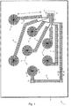
- FIG. 1 a user interface sheet 1 for capacitive sensing in accordance with the present invention is shown.
- the sheet 1 comprises a substrate 2 which supports a plurality of conductive elements 3 of a first type distributed across the substrate 2, a set of terminals 4 and a plurality of conductive elements 5 of a second type. As shown in Figure 1 , the terminals 4 are grouped in an area 6 to which a device or connector can be attached and make contact with the terminals 4.
- the first type of conductive elements 3 are for capacitive sensing and are hereinafter referred to as “capacitive sensing elements” or “capacitive sensors”.
- the second type of conductive elements 5 are for connecting the capacitive sensing elements 3 to single tracks 7 which in turn are connected to the terminals 4.
- the second type of conductive elements 5 are hereinafter referred to as “connecting elements” or “connectors”.
- the connecting elements 5 may include one or more turns 8.
- two or more capacitive sensing elements 3 may be connected by one or more connecting elements 5, i.e. forming a series of linked capacitive sensing elements 3.
- Each capacitive sensing element 3 serves as a single key capacitive touch or proximity switch.
- the substrate 2 comprises an electrically insulating material and is flexible.
- the substrate 2 comprises a sheet of thick paper or card having a weight, for example, of about 100 to about 200 g/m2.
- the substrate 2 may have a weight of up to 350 g/m 2 or more.
- plastics materials such as polyethylene terephthalate (PET)
- PET polyethylene terephthalate
- the substrate 2 may be rigid or stiff.
- the substrate 2 may comprise paperboard, cardboard, hardboard or thick plastic.
- the substrate 2 and/or the conductive elements 3, 5 may be opaque, i.e. non-transparent.
- the substrate 2 may support printed indicia (not shown), such as text and/or graphics.
- the printed indicia (not shown) may cover the conductive elements 3, 5.
- a protective layer may cover the conductive elements 3, 5.
- the protective layer (not shown) may be transparent or opaque and may support printed indicia (not shown), such as text and/or graphics.
- the protective layer (not shown) may comprise paper or card or plastic.
- the protective layer (not shown) may be glued to the sheet 2 or be laminated.
- the substrate material has a relative dielectric constant, ⁇ r .
- the relative dielectric constant may be between about 2 and 4 or more.
- the sheet 1 has dimensions of 297 ⁇ 420 mm, i.e. A3 as defined by International Standards Organization (ISO) 216.
- the sheet 1 can be larger, for example A0, A1 or A2, or smaller, for instance, A4 or A5.
- the capacitive sensing elements 3 take the form of circular conductive pads, i.e. conductive discs.
- the capacitive sensing elements 3 each have a radius, r, of about 30 mm.
- the capacitive sensing elements 3 can be larger or smaller. Furthermore, all of the capacitive sensing elements 3 need not be the same size.
- each capacitive sensing element 3 comprises a pad 9 comprising relatively low conductivity material, in this case carbon-based conductive ink, and a conductive skeleton or mesh 10 comprising relatively high conductivity material, in this case silver-based conductive ink, overlying the pad 9 so as to form a composite structure.
- the sheet resistance of the pad 9 may be at least 1 k ⁇ sq -1 and may typically lie in a range of 10 to 50 k ⁇ sq -1 .
- the sheet resistance of (a solid block of) the mesh 10 may be no more than 10 ⁇ sq -1 and may typically lie in a range of 1 to 5 ⁇ sq -1 .
- the pad 9 and mesh 10 have approximately the same thickness lying in a range of about 0.5 to 10 ⁇ m, typically in a range of about 1 to 5 ⁇ m. n this example, no further overlying or underlying layers of conductive material are included in the composite structure.
- the pad 9 comprises a single solid block of conductive material.
- the pad 9 can include voids or slots, and/or be broken up into discrete blocks of material.
- the conductive mesh 10 comprises a circular array of m concentric rings 11 and n spokes 12 and has a dart board-like appearance in plan view.
- the rings 11 are radially equally spaced from neighbouring rings 11 by a distance, ⁇ r, and the spokes 12 are angularly equally spaced from neighbouring spokes by an angle, ⁇ .
- the rings 11 have a first line width, w 1
- the spokes 12 have a second line width, w 2 .
- the rings 11 and spokes 12 may have different line widths from each other and/or may be thicker or thinner, e.g. about 500 ⁇ m.
- the capacitive sensing elements 3 need not be circular and the conductive mesh 10 can have other, non-circular shapes.
- a capacitive sensing element 3 can be oval, rectangular (for example square) or polygonal, or be a non-regular or non-uniform shape.
- the conductive mesh 10 need not be a circular array, but can be a rectangular array or take any shape, which may be non-regular or non-uniform and/or which may include non periodic features or members.
- the members 11, 12 of the mesh 10 need not cross at right angles. Furthermore, the members 11, 12 of the mesh need not define identically shaped and/or identically sized open regions.
- the mesh 10 may comprise only one node, for example a set of spokes 12 joined in the middle.
- the mesh 10 may take the form of a fibrous line which comprises an elongate line with shorter lines crossing the line along its length.
- the elongate line can provide a highly conductive backbone or trunk and the shorter lines can provide highly conductive branches.
- Multiple fibrous lines can be connected to form a fibrous mesh or network.
- a mesh comprising, for example, an array of lines, may additionally be provided with shorter lines to form, for example, a fibrous array.
- the conductive mesh 10 need not comprise conductive ink.
- the conductive mesh 10 may comprise a metal foil, for example formed by hot or cold foil stamping.
- the conductive mesh 10 need not overlie the conductive pad 9.
- the conductive mesh 10 can lie under the conductive pad 9.
- two or more conductive pads 9 and/or conductive meshes 10 can be provided in a stacked structure or sandwich arrangement.
- the conductive pad 9 may take the form of discrete blocks of conductive material with open regions of the mesh 10 filled with the discrete blocks of the conductive material, i.e. most of the pad 9 and most of the mesh 10 are co-planar. As will be explained in more detail hereinafter, this arrangement can be achieved using a so-called "reversing out" process.
- the capacitive sensing element 3 has a lower sheet resistance than a capacitive sensing element which only uses the relatively low conductivity material.
- each connecting element 5 comprises a set of elongate conductive tracks 13 and a set of conductive members 14 crossing the tracks (hereinafter referred to as “crossing members” or “linking members”).
- the connecting element 5 comprises silver-based conductive ink, that is, the same material used to form the conductive meshes 10 ( Figure 1a ).
- a connecting element 5 can have a length, L, of between about 10 mm and about 500 mm. However, the length of a connecting element 5 can exceed 500 mm.
- the elongate conductive tracks 13 form a band having a width, w.
- the connecting element 5 comprises p tracks 13 and q crossing members 14 per centimetre.
- the cross-linking members 14 run across the tracks 13 perpendicularly.
- the crossing members 14 extend between outer tracks of the connecting element 5 linking the tracks. However, a crossing member 14 need not cross all the tracks 13.
- the tracks 13 have a third line width, w 3
- the crossing members 14 have a fourth line width, w 4 .
- the tracks 13 and crossing members 14 may have different line widths from each other and may be thicker or thinner, e.g. about 500 ⁇ m.
- the connecting element 5 can be thought of as a single track which has been divided into separate narrow tracks which have been spaced apart. If the user places their finger over the connecting element 5, then there is less capacitive coupling. If the width of the conducting element 5 is greater than the width of a finger, then capacitive coupling will greatly reduced.
- Each connecting element 5 preferably has a capacitance C c (between a conductive element 3 and a terminal 4) such that C c ⁇ 0.2 ⁇ C p or C c ⁇ 0.1 ⁇ C p , where C p is the capacitance of the conducting element 5.
- Each connecting element 5 preferably has a resistance R c (between a conductive element 3 and terminal 4) such that R c ⁇ 10k ⁇ or R c ⁇ 5kQ.
- the use of the crossing members 14 can help to link tracks 13 and so minimise the effect of defects and/or breaks.
- the conductive elements 3, terminals 4 and tracks 5 can be formed using a printing process, such as screen printing, ink jet printing, flexography or offset printing.
- a first printer 15 e.g. an inkjet, offset or screen printer, is used to apply a first ink 16 on to the substrate 2.
- the first ink 16 comprises a carbon-based conductive ink and is used to form conductive pads 9.
- the ink 16 is left sufficiently long to dry or is cured to allow a further layer of ink to be printed.
- a second printer 17 e.g. an inkjet, offset or screen printer, is used to apply a second ink 18 on to the sheet 2.
- the second ink 18 comprises a silver-based conductive ink is used to form the terminals 4 ( Figure 1 ), the connecting element 5 and the conductive mesh 10.
- Suitable conductive inks are available from Sun Chemical Corporation, Parsippany, New Jersey, USA.
- the relatively high conductivity ink can be replaced by a metal foil, for example, comprising aluminium or silver.
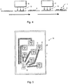
- the interactive printed article 19 takes the form of an interactive poster.
- a sheet 1 is placed behind a poster 20 having indicia 21 printed thereon and so provide a user interface.
- a single sheet may be used, in other words, one side of the sheet supports the user interface and the reverse supports printed indicia.
- the capacitive sensing elements 3 can be aligned with some of the indicia 21 in places which guide, invite or instruct a user to touch the poster in those places.
- a device 22 is mounted to the sheet 1 which alone or in conjunction with other circuitry can provide audio and/or visual output.
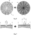
- a printing line is used to form the capacitive sensing element 3, then it may be printed "wet-on-wet", i.e. the conductive mesh 10 is printed on the conductive pad 9 while the ink forming the conductive pad 9 is still wet.
- this may result in intermixing of the inks, which can reduce the conductivity of the conductive mesh 10.
- One solution is to wait sufficiently long, for example a few hours, between printing the conductive pad 9 and printing the conductive mesh 10 for the ink of the conductive pad 9 to dry.
- a modified form of conductive pad 9' can be printed.
- the conductive pad 9' is made up of regions 22 of ink with a reversed-out image 23 of, in this example, the conductive mesh 10.
- the gaps making up the image 23 have a width, w5, for example of about 0.5 mm.
- a conductive mesh which can be the same as the conductive mesh 10 ( Figure 1a ) described earlier, is then printed on top having a line width, w 6 , where w 6 > w 5 , for example, 1 mm.
- intermixed mesh 24 comprising a first, central region 25 comprising material which has a high conductivity and a second, interface region 26 which comprises a mixture of the inks which has a lower conductivity than the ink in the first region 25.
- pattern of the pad and mesh can differ, as hereinbefore described. It will also be appreciated that the order of printing may be reversed, i.e. the conductive mesh is printed first and then the conductive pad 9' is printed.
- the interactive printed article need not be a poster, but can be a book, calendar, greeting card, product packaging or point of sale display.
- the substrate can be any form of fibre-based material, such as paper or card.
- a sheet 1 which supports capacitive sensing elements 3 and connecting elements 5 may be applied to another article.
- the sheet 1 may line an injection moulding die (not shown) and material such as plastic (not shown) may be injected into the die to form an article (not shown) which includes the sheet 1, for example covering it surface. Therefore, capacitive sensing elements 3 can be easily incorporated into an article which, for example, has a complex shape.
Landscapes
- Laminated Bodies (AREA)
- Inks, Pencil-Leads, Or Crayons (AREA)
- Switches That Are Operated By Magnetic Or Electric Fields (AREA)
- Shielding Devices Or Components To Electric Or Magnetic Fields (AREA)
- Parts Printed On Printed Circuit Boards (AREA)
- Position Input By Displaying (AREA)
- Manufacture Of Switches (AREA)
- Investigating Or Analyzing Materials By The Use Of Electric Means (AREA)
- Non-Adjustable Resistors (AREA)
Priority Applications (1)
| Application Number | Priority Date | Filing Date | Title |
|---|---|---|---|
| EP18196507.0A EP3468040B1 (en) | 2011-01-28 | 2012-01-27 | Conductive element |
Applications Claiming Priority (2)
| Application Number | Priority Date | Filing Date | Title |
|---|---|---|---|
| GB1101510.4A GB2487579B (en) | 2011-01-28 | 2011-01-28 | Printed article with at least one capacitive touch switch |
| PCT/GB2012/050171 WO2012101448A2 (en) | 2011-01-28 | 2012-01-27 | Conductive element |
Related Child Applications (1)
| Application Number | Title | Priority Date | Filing Date |
|---|---|---|---|
| EP18196507.0A Division EP3468040B1 (en) | 2011-01-28 | 2012-01-27 | Conductive element |
Publications (2)
| Publication Number | Publication Date |
|---|---|
| EP2668721A2 EP2668721A2 (en) | 2013-12-04 |
| EP2668721B1 true EP2668721B1 (en) | 2018-09-26 |
Family
ID=43824753
Family Applications (2)
| Application Number | Title | Priority Date | Filing Date |
|---|---|---|---|
| EP12703145.8A Active EP2668721B1 (en) | 2011-01-28 | 2012-01-27 | Conductive element |
| EP18196507.0A Active EP3468040B1 (en) | 2011-01-28 | 2012-01-27 | Conductive element |
Family Applications After (1)
| Application Number | Title | Priority Date | Filing Date |
|---|---|---|---|
| EP18196507.0A Active EP3468040B1 (en) | 2011-01-28 | 2012-01-27 | Conductive element |
Country Status (8)
Families Citing this family (16)
| Publication number | Priority date | Publication date | Assignee | Title |
|---|---|---|---|---|
| US9916045B2 (en) | 2009-10-26 | 2018-03-13 | Amtel Corporation | Sense electrode design |
| DE102012002193B4 (de) * | 2012-02-07 | 2021-07-29 | Polyic Gmbh & Co. Kg | Kapazitives Sensorelement |
| WO2013176825A1 (en) | 2012-05-23 | 2013-11-28 | SmartBound Technologies, LLC | Interactive printed article with touch-activated presentation |
| GB2501570B (en) | 2012-12-18 | 2014-04-16 | Novalia Ltd | Capacitive touch device |
| JP5958872B2 (ja) * | 2014-06-13 | 2016-08-02 | 学校法人明治大学 | 入力装置、情報処理装置及びヘッドマウントディスプレイ |
| GB2523216B (en) * | 2014-10-17 | 2016-01-27 | Novalia Ltd | Capacitive touch device |
| GB2531339B (en) * | 2014-10-17 | 2018-03-21 | Novalia Ltd | Capacitive touch device |
| DE102016221412B4 (de) * | 2015-11-04 | 2024-03-21 | Gentherm Inc. | Quetschverbindung für geflechtartiges Abschirmmaterial zur Verwendung in mit kapazitiven Sensoren ausgestatteten Lenkrädern |
| JP2018040776A (ja) * | 2016-09-09 | 2018-03-15 | 株式会社NejiLaw | センサ構造、センサ構造付部材 |
| US10480962B2 (en) * | 2017-04-21 | 2019-11-19 | Capsule Technologies, Inc. | Electronic device including a capacitive sensor in a housing |
| KR20230093362A (ko) * | 2017-06-30 | 2023-06-27 | 스노우슈푸드 인크. | 내장형 트레이스 용량성 시그넷 스탬프 |
| KR102259995B1 (ko) * | 2017-10-30 | 2021-06-02 | 니뽄 도쿠슈 도교 가부시키가이샤 | 전극 매설 부재 |
| JP6901420B2 (ja) * | 2018-03-02 | 2021-07-14 | ヤフー株式会社 | 情報制御プログラム、情報制御方法および情報制御装置 |
| US10754480B2 (en) | 2018-04-26 | 2020-08-25 | Hewlett-Packard Development Company, L.P. | Frames for interactive posters |
| DE102021003493A1 (de) | 2021-07-06 | 2023-01-12 | Giesecke+Devrient Currency Technology Gmbh | Sicherheitsdokument und Verfahren zur Herstellung eines Sicherheitsdokuments |
| GB202205271D0 (en) | 2022-04-11 | 2022-05-25 | Novalia Ltd | Image processing |
Family Cites Families (38)
| Publication number | Priority date | Publication date | Assignee | Title |
|---|---|---|---|---|
| US4920342A (en) * | 1988-10-25 | 1990-04-24 | W. H. Brady Co. | Membrane switchcores with high resisitivity ink circuits |
| US7911456B2 (en) * | 1992-06-08 | 2011-03-22 | Synaptics Incorporated | Object position detector with edge motion feature and gesture recognition |
| GB9406702D0 (en) | 1994-04-05 | 1994-05-25 | Binstead Ronald P | Multiple input proximity detector and touchpad system |
| JPH09153667A (ja) * | 1995-11-29 | 1997-06-10 | Mitsumi Electric Co Ltd | 回路基盤 |
| JPH10294022A (ja) * | 1997-04-18 | 1998-11-04 | Kanto Bussan Kk | 導電フィルム |
| SE526367C2 (sv) * | 2003-02-28 | 2005-08-30 | Sca Packaging Sweden Ab | Affisch med tryckta zoner för inmatning till en elektronisk krets |
| US7138170B2 (en) * | 2003-04-28 | 2006-11-21 | Eastman Kodak Company | Terminated conductive patterned sheet utilizing conductive conduits |
| US20050030048A1 (en) * | 2003-08-05 | 2005-02-10 | Bolender Robert J. | Capacitive sensing device for use in a keypad assembly |
| JP4610416B2 (ja) * | 2005-06-10 | 2011-01-12 | 日本写真印刷株式会社 | 静電容量型タッチパネル |
| EP1897017A1 (de) * | 2005-06-30 | 2008-03-12 | Siemens Aktiengesellschaft | Hardwareschutz in form von zu halbschalen tiefgezogenen leiterplatten |
| US20070158621A1 (en) * | 2005-07-19 | 2007-07-12 | Kyocera Corporation | Conductive Paste, Solar Cell Manufactured Using Conductive Paste, Screen Printing Method and Solar Cell Formed Using Screen Printing Method |
| GB2429111A (en) * | 2005-08-10 | 2007-02-14 | Nicholas Jim Stone | Electronic tag |
| CN101268501B (zh) * | 2005-09-20 | 2011-04-13 | 大卫·诺里斯·肯莱特 | 接近响应显示材料的装置和方法 |
| JP4733184B2 (ja) * | 2006-06-12 | 2011-07-27 | シャープ株式会社 | タッチパネル、表示装置及びタッチパネルの製造方法 |
| CN101410779A (zh) * | 2006-06-12 | 2009-04-15 | 夏普株式会社 | 触摸面板、显示装置和触摸面板的制造方法 |
| WO2008038764A1 (fr) | 2006-09-28 | 2008-04-03 | Fujifilm Corporation | Écran à émission spontanée, procédé de fabrication d'un écran à émission spontanée, film conducteur transparent, dispositif électroluminescent, électrode transparente de cellule solaire et électrode transparente de papier électronique |
| JP2008130449A (ja) | 2006-11-22 | 2008-06-05 | Alps Electric Co Ltd | 発光装置およびその製造方法 |
| US8373664B2 (en) * | 2006-12-18 | 2013-02-12 | Cypress Semiconductor Corporation | Two circuit board touch-sensor device |
| CN101553776B (zh) * | 2007-02-08 | 2011-11-23 | 夏普株式会社 | 触摸面板装置及其制造方法 |
| US7528337B2 (en) * | 2007-05-15 | 2009-05-05 | Panasonic Corporation | Pressure sensitive conductive sheet and panel switch using same |
| JP2008311208A (ja) * | 2007-05-15 | 2008-12-25 | Panasonic Corp | 感圧導電シート及びこれを用いたパネルスイッチ |
| CN101464757A (zh) * | 2007-12-21 | 2009-06-24 | 清华大学 | 触摸屏及显示装置 |
| TWI438906B (zh) * | 2007-12-20 | 2014-05-21 | Cima Nanotech Israel Ltd | 具有利用奈米粒子形成的透明電極之光伏打裝置 |
| DE102008004423B4 (de) * | 2008-01-14 | 2011-01-20 | Fela Holding Gmbh | Anordnung zur Erfassung von Berührungen auf einer Trägerplatte und Verfahren zur Herstellung eines Sensors |
| WO2009108771A2 (en) | 2008-02-28 | 2009-09-03 | 3M Innovative Properties Company | Methods of patterning a conductor on a substrate |
| US9823784B2 (en) * | 2008-04-10 | 2017-11-21 | Atmel Corporation | Capacitive touch screen with noise suppression |
| KR101329638B1 (ko) * | 2008-07-31 | 2013-11-14 | 군제 가부시키가이샤 | 평면체 및 터치 스위치 |
| US8269744B2 (en) * | 2008-09-05 | 2012-09-18 | Mitsubishi Electric Corporation | Touch screen, touch panel and display device |
| JP4985717B2 (ja) * | 2008-12-04 | 2012-07-25 | 大日本印刷株式会社 | 有機薄膜太陽電池およびその製造方法 |
| US8749496B2 (en) * | 2008-12-05 | 2014-06-10 | Apple Inc. | Integrated touch panel for a TFT display |
| JP5045733B2 (ja) * | 2008-12-24 | 2012-10-10 | 株式会社デンソー | 半導体装置 |
| CN101783395A (zh) * | 2009-01-20 | 2010-07-21 | 京东方科技集团股份有限公司 | 有机电致发光器件及其制造方法 |
| EP2405328A4 (en) * | 2009-03-04 | 2013-10-02 | Dong Sik Nam | TOUCH SCREEN SENSOR |
| KR100944519B1 (ko) | 2009-03-04 | 2010-03-03 | 남동식 | 터치패널센서 |
| JP5174745B2 (ja) * | 2009-06-09 | 2013-04-03 | グンゼ株式会社 | タッチスイッチ |
| US20110012845A1 (en) * | 2009-07-20 | 2011-01-20 | Rothkopf Fletcher R | Touch sensor structures for displays |
| BR112012018856A2 (pt) * | 2010-01-28 | 2017-12-12 | Fujifilm Corp | folha condutora, método para usar a mesma e painel sensível ao toque |
| JP5248653B2 (ja) * | 2010-05-27 | 2013-07-31 | 富士フイルム株式会社 | 導電シート及び静電容量方式タッチパネル |
-
2011
- 2011-01-28 GB GB1101510.4A patent/GB2487579B/en active Active
- 2011-01-28 GB GB1311340.2A patent/GB2505291B/en active Active
- 2011-01-28 GB GB1311341.0A patent/GB2505292B/en not_active Expired - Fee Related
-
2012
- 2012-01-27 CN CN201280015720.4A patent/CN103460601B/zh active Active
- 2012-01-27 WO PCT/GB2012/050171 patent/WO2012101448A2/en active Application Filing
- 2012-01-27 CN CN201710667080.XA patent/CN107483042B/zh active Active
- 2012-01-27 US US13/982,078 patent/US9425790B2/en active Active
- 2012-01-27 JP JP2013550953A patent/JP5986109B2/ja active Active
- 2012-01-27 EP EP12703145.8A patent/EP2668721B1/en active Active
- 2012-01-27 CA CA2825853A patent/CA2825853A1/en not_active Abandoned
- 2012-01-27 BR BR112013019254A patent/BR112013019254A2/pt not_active IP Right Cessation
- 2012-01-27 EP EP18196507.0A patent/EP3468040B1/en active Active
Also Published As
| Publication number | Publication date |
|---|---|
| GB2487579A (en) | 2012-08-01 |
| GB2505292B (en) | 2015-06-10 |
| CN107483042A (zh) | 2017-12-15 |
| CN103460601A (zh) | 2013-12-18 |
| EP3468040A1 (en) | 2019-04-10 |
| WO2012101448A3 (en) | 2012-11-08 |
| BR112013019254A2 (pt) | 2016-11-22 |
| CA2825853A1 (en) | 2012-08-02 |
| WO2012101448A2 (en) | 2012-08-02 |
| JP2014506694A (ja) | 2014-03-17 |
| GB2505291A (en) | 2014-02-26 |
| US20140021027A1 (en) | 2014-01-23 |
| JP5986109B2 (ja) | 2016-09-06 |
| US9425790B2 (en) | 2016-08-23 |
| GB2487579B (en) | 2015-07-22 |
| GB2505291B (en) | 2015-08-12 |
| GB201311340D0 (en) | 2013-08-14 |
| GB201101510D0 (en) | 2011-03-16 |
| EP3468040B1 (en) | 2020-09-09 |
| CN107483042B (zh) | 2021-03-30 |
| GB2505292A (en) | 2014-02-26 |
| EP2668721A2 (en) | 2013-12-04 |
| GB201311341D0 (en) | 2013-08-14 |
| CN103460601B (zh) | 2017-09-22 |
Similar Documents
| Publication | Publication Date | Title |
|---|---|---|
| EP2668721B1 (en) | Conductive element | |
| US9762235B2 (en) | Touch-sensitive input device | |
| EP3207441B1 (en) | Capacitive touch device | |
| KR20180117768A (ko) | 터치 센서, 이를 포함하는 표시 장치, 및 터치 센서의 제조 방법 | |
| EP3206883B1 (en) | Capacitive touch device | |
| CA2895446C (en) | Capacitive coupling | |
| JP5520776B2 (ja) | センサーシートおよびその製造方法 | |
| WO2013128205A1 (en) | Circuit board assembly | |
| EP3206882A1 (en) | Printed article | |
| GB2487580A (en) | Sheet for user interface with capacitive sensing elements | |
| WO2017037414A1 (en) | Fabricating a touch-sensitive input device | |
| CN203386173U (zh) | 单层多点式触控导电膜及单层多点式触控屏 |
Legal Events
| Date | Code | Title | Description |
|---|---|---|---|
| PUAI | Public reference made under article 153(3) epc to a published international application that has entered the european phase |
Free format text: ORIGINAL CODE: 0009012 |
|
| 17P | Request for examination filed |
Effective date: 20130731 |
|
| AK | Designated contracting states |
Kind code of ref document: A2 Designated state(s): AL AT BE BG CH CY CZ DE DK EE ES FI FR GB GR HR HU IE IS IT LI LT LU LV MC MK MT NL NO PL PT RO RS SE SI SK SM TR |
|
| DAX | Request for extension of the european patent (deleted) | ||
| GRAP | Despatch of communication of intention to grant a patent |
Free format text: ORIGINAL CODE: EPIDOSNIGR1 |
|
| STAA | Information on the status of an ep patent application or granted ep patent |
Free format text: STATUS: GRANT OF PATENT IS INTENDED |
|
| INTG | Intention to grant announced |
Effective date: 20180409 |
|
| GRAS | Grant fee paid |
Free format text: ORIGINAL CODE: EPIDOSNIGR3 |
|
| GRAA | (expected) grant |
Free format text: ORIGINAL CODE: 0009210 |
|
| STAA | Information on the status of an ep patent application or granted ep patent |
Free format text: STATUS: THE PATENT HAS BEEN GRANTED |
|
| AK | Designated contracting states |
Kind code of ref document: B1 Designated state(s): AL AT BE BG CH CY CZ DE DK EE ES FI FR GB GR HR HU IE IS IT LI LT LU LV MC MK MT NL NO PL PT RO RS SE SI SK SM TR |
|
| REG | Reference to a national code |
Ref country code: GB Ref legal event code: FG4D |
|
| REG | Reference to a national code |
Ref country code: CH Ref legal event code: EP |
|
| REG | Reference to a national code |
Ref country code: AT Ref legal event code: REF Ref document number: 1047229 Country of ref document: AT Kind code of ref document: T Effective date: 20181015 |
|
| REG | Reference to a national code |
Ref country code: IE Ref legal event code: FG4D |
|
| REG | Reference to a national code |
Ref country code: DE Ref legal event code: R096 Ref document number: 602012051479 Country of ref document: DE |
|
| REG | Reference to a national code |
Ref country code: NL Ref legal event code: MP Effective date: 20180926 |
|
| PG25 | Lapsed in a contracting state [announced via postgrant information from national office to epo] |
Ref country code: SE Free format text: LAPSE BECAUSE OF FAILURE TO SUBMIT A TRANSLATION OF THE DESCRIPTION OR TO PAY THE FEE WITHIN THE PRESCRIBED TIME-LIMIT Effective date: 20180926 Ref country code: GR Free format text: LAPSE BECAUSE OF FAILURE TO SUBMIT A TRANSLATION OF THE DESCRIPTION OR TO PAY THE FEE WITHIN THE PRESCRIBED TIME-LIMIT Effective date: 20181227 Ref country code: RS Free format text: LAPSE BECAUSE OF FAILURE TO SUBMIT A TRANSLATION OF THE DESCRIPTION OR TO PAY THE FEE WITHIN THE PRESCRIBED TIME-LIMIT Effective date: 20180926 Ref country code: NO Free format text: LAPSE BECAUSE OF FAILURE TO SUBMIT A TRANSLATION OF THE DESCRIPTION OR TO PAY THE FEE WITHIN THE PRESCRIBED TIME-LIMIT Effective date: 20181226 Ref country code: LT Free format text: LAPSE BECAUSE OF FAILURE TO SUBMIT A TRANSLATION OF THE DESCRIPTION OR TO PAY THE FEE WITHIN THE PRESCRIBED TIME-LIMIT Effective date: 20180926 Ref country code: BG Free format text: LAPSE BECAUSE OF FAILURE TO SUBMIT A TRANSLATION OF THE DESCRIPTION OR TO PAY THE FEE WITHIN THE PRESCRIBED TIME-LIMIT Effective date: 20181226 Ref country code: FI Free format text: LAPSE BECAUSE OF FAILURE TO SUBMIT A TRANSLATION OF THE DESCRIPTION OR TO PAY THE FEE WITHIN THE PRESCRIBED TIME-LIMIT Effective date: 20180926 |
|
| REG | Reference to a national code |
Ref country code: LT Ref legal event code: MG4D |
|
| PG25 | Lapsed in a contracting state [announced via postgrant information from national office to epo] |
Ref country code: LV Free format text: LAPSE BECAUSE OF FAILURE TO SUBMIT A TRANSLATION OF THE DESCRIPTION OR TO PAY THE FEE WITHIN THE PRESCRIBED TIME-LIMIT Effective date: 20180926 Ref country code: AL Free format text: LAPSE BECAUSE OF FAILURE TO SUBMIT A TRANSLATION OF THE DESCRIPTION OR TO PAY THE FEE WITHIN THE PRESCRIBED TIME-LIMIT Effective date: 20180926 Ref country code: HR Free format text: LAPSE BECAUSE OF FAILURE TO SUBMIT A TRANSLATION OF THE DESCRIPTION OR TO PAY THE FEE WITHIN THE PRESCRIBED TIME-LIMIT Effective date: 20180926 |
|
| REG | Reference to a national code |
Ref country code: AT Ref legal event code: MK05 Ref document number: 1047229 Country of ref document: AT Kind code of ref document: T Effective date: 20180926 |
|
| PG25 | Lapsed in a contracting state [announced via postgrant information from national office to epo] |
Ref country code: IT Free format text: LAPSE BECAUSE OF FAILURE TO SUBMIT A TRANSLATION OF THE DESCRIPTION OR TO PAY THE FEE WITHIN THE PRESCRIBED TIME-LIMIT Effective date: 20180926 Ref country code: EE Free format text: LAPSE BECAUSE OF FAILURE TO SUBMIT A TRANSLATION OF THE DESCRIPTION OR TO PAY THE FEE WITHIN THE PRESCRIBED TIME-LIMIT Effective date: 20180926 Ref country code: ES Free format text: LAPSE BECAUSE OF FAILURE TO SUBMIT A TRANSLATION OF THE DESCRIPTION OR TO PAY THE FEE WITHIN THE PRESCRIBED TIME-LIMIT Effective date: 20180926 Ref country code: AT Free format text: LAPSE BECAUSE OF FAILURE TO SUBMIT A TRANSLATION OF THE DESCRIPTION OR TO PAY THE FEE WITHIN THE PRESCRIBED TIME-LIMIT Effective date: 20180926 Ref country code: IS Free format text: LAPSE BECAUSE OF FAILURE TO SUBMIT A TRANSLATION OF THE DESCRIPTION OR TO PAY THE FEE WITHIN THE PRESCRIBED TIME-LIMIT Effective date: 20190126 Ref country code: PL Free format text: LAPSE BECAUSE OF FAILURE TO SUBMIT A TRANSLATION OF THE DESCRIPTION OR TO PAY THE FEE WITHIN THE PRESCRIBED TIME-LIMIT Effective date: 20180926 Ref country code: RO Free format text: LAPSE BECAUSE OF FAILURE TO SUBMIT A TRANSLATION OF THE DESCRIPTION OR TO PAY THE FEE WITHIN THE PRESCRIBED TIME-LIMIT Effective date: 20180926 Ref country code: CZ Free format text: LAPSE BECAUSE OF FAILURE TO SUBMIT A TRANSLATION OF THE DESCRIPTION OR TO PAY THE FEE WITHIN THE PRESCRIBED TIME-LIMIT Effective date: 20180926 Ref country code: NL Free format text: LAPSE BECAUSE OF FAILURE TO SUBMIT A TRANSLATION OF THE DESCRIPTION OR TO PAY THE FEE WITHIN THE PRESCRIBED TIME-LIMIT Effective date: 20180926 |
|
| PG25 | Lapsed in a contracting state [announced via postgrant information from national office to epo] |
Ref country code: SM Free format text: LAPSE BECAUSE OF FAILURE TO SUBMIT A TRANSLATION OF THE DESCRIPTION OR TO PAY THE FEE WITHIN THE PRESCRIBED TIME-LIMIT Effective date: 20180926 Ref country code: PT Free format text: LAPSE BECAUSE OF FAILURE TO SUBMIT A TRANSLATION OF THE DESCRIPTION OR TO PAY THE FEE WITHIN THE PRESCRIBED TIME-LIMIT Effective date: 20190126 Ref country code: SK Free format text: LAPSE BECAUSE OF FAILURE TO SUBMIT A TRANSLATION OF THE DESCRIPTION OR TO PAY THE FEE WITHIN THE PRESCRIBED TIME-LIMIT Effective date: 20180926 |
|
| REG | Reference to a national code |
Ref country code: DE Ref legal event code: R097 Ref document number: 602012051479 Country of ref document: DE |
|
| PG25 | Lapsed in a contracting state [announced via postgrant information from national office to epo] |
Ref country code: DK Free format text: LAPSE BECAUSE OF FAILURE TO SUBMIT A TRANSLATION OF THE DESCRIPTION OR TO PAY THE FEE WITHIN THE PRESCRIBED TIME-LIMIT Effective date: 20180926 |
|
| PLBE | No opposition filed within time limit |
Free format text: ORIGINAL CODE: 0009261 |
|
| STAA | Information on the status of an ep patent application or granted ep patent |
Free format text: STATUS: NO OPPOSITION FILED WITHIN TIME LIMIT |
|
| PG25 | Lapsed in a contracting state [announced via postgrant information from national office to epo] |
Ref country code: MC Free format text: LAPSE BECAUSE OF FAILURE TO SUBMIT A TRANSLATION OF THE DESCRIPTION OR TO PAY THE FEE WITHIN THE PRESCRIBED TIME-LIMIT Effective date: 20180926 |
|
| REG | Reference to a national code |
Ref country code: CH Ref legal event code: PL |
|
| 26N | No opposition filed |
Effective date: 20190627 |
|
| PG25 | Lapsed in a contracting state [announced via postgrant information from national office to epo] |
Ref country code: LU Free format text: LAPSE BECAUSE OF NON-PAYMENT OF DUE FEES Effective date: 20190127 |
|
| REG | Reference to a national code |
Ref country code: BE Ref legal event code: MM Effective date: 20190131 |
|
| REG | Reference to a national code |
Ref country code: IE Ref legal event code: MM4A |
|
| PG25 | Lapsed in a contracting state [announced via postgrant information from national office to epo] |
Ref country code: SI Free format text: LAPSE BECAUSE OF FAILURE TO SUBMIT A TRANSLATION OF THE DESCRIPTION OR TO PAY THE FEE WITHIN THE PRESCRIBED TIME-LIMIT Effective date: 20180926 |
|
| PG25 | Lapsed in a contracting state [announced via postgrant information from national office to epo] |
Ref country code: BE Free format text: LAPSE BECAUSE OF NON-PAYMENT OF DUE FEES Effective date: 20190131 |
|
| PG25 | Lapsed in a contracting state [announced via postgrant information from national office to epo] |
Ref country code: LI Free format text: LAPSE BECAUSE OF NON-PAYMENT OF DUE FEES Effective date: 20190131 Ref country code: CH Free format text: LAPSE BECAUSE OF NON-PAYMENT OF DUE FEES Effective date: 20190131 |
|
| PG25 | Lapsed in a contracting state [announced via postgrant information from national office to epo] |
Ref country code: IE Free format text: LAPSE BECAUSE OF NON-PAYMENT OF DUE FEES Effective date: 20190127 |
|
| REG | Reference to a national code |
Ref country code: GB Ref legal event code: 746 Effective date: 20200303 |
|
| PG25 | Lapsed in a contracting state [announced via postgrant information from national office to epo] |
Ref country code: TR Free format text: LAPSE BECAUSE OF FAILURE TO SUBMIT A TRANSLATION OF THE DESCRIPTION OR TO PAY THE FEE WITHIN THE PRESCRIBED TIME-LIMIT Effective date: 20180926 |
|
| PG25 | Lapsed in a contracting state [announced via postgrant information from national office to epo] |
Ref country code: MT Free format text: LAPSE BECAUSE OF NON-PAYMENT OF DUE FEES Effective date: 20190127 |
|
| REG | Reference to a national code |
Ref country code: DE Ref legal event code: R082 Ref document number: 602012051479 Country of ref document: DE Representative=s name: VENNER SHIPLEY GERMANY LLP, DE Ref country code: DE Ref legal event code: R082 Ref document number: 602012051479 Country of ref document: DE Representative=s name: VENNER SHIPLEY LLP, DE |
|
| PG25 | Lapsed in a contracting state [announced via postgrant information from national office to epo] |
Ref country code: CY Free format text: LAPSE BECAUSE OF FAILURE TO SUBMIT A TRANSLATION OF THE DESCRIPTION OR TO PAY THE FEE WITHIN THE PRESCRIBED TIME-LIMIT Effective date: 20180926 |
|
| PG25 | Lapsed in a contracting state [announced via postgrant information from national office to epo] |
Ref country code: HU Free format text: LAPSE BECAUSE OF FAILURE TO SUBMIT A TRANSLATION OF THE DESCRIPTION OR TO PAY THE FEE WITHIN THE PRESCRIBED TIME-LIMIT; INVALID AB INITIO Effective date: 20120127 |
|
| REG | Reference to a national code |
Ref country code: DE Ref legal event code: R084 Ref document number: 602012051479 Country of ref document: DE |
|
| PG25 | Lapsed in a contracting state [announced via postgrant information from national office to epo] |
Ref country code: MK Free format text: LAPSE BECAUSE OF FAILURE TO SUBMIT A TRANSLATION OF THE DESCRIPTION OR TO PAY THE FEE WITHIN THE PRESCRIBED TIME-LIMIT Effective date: 20180926 |
|
| PGFP | Annual fee paid to national office [announced via postgrant information from national office to epo] |
Ref country code: DE Payment date: 20240119 Year of fee payment: 13 Ref country code: GB Payment date: 20240117 Year of fee payment: 13 |
|
| PGFP | Annual fee paid to national office [announced via postgrant information from national office to epo] |
Ref country code: FR Payment date: 20240124 Year of fee payment: 13 |