EP2668526B1 - Lasermarkierte vorrichtung - Google Patents
Lasermarkierte vorrichtung Download PDFInfo
- Publication number
- EP2668526B1 EP2668526B1 EP12715241.1A EP12715241A EP2668526B1 EP 2668526 B1 EP2668526 B1 EP 2668526B1 EP 12715241 A EP12715241 A EP 12715241A EP 2668526 B1 EP2668526 B1 EP 2668526B1
- Authority
- EP
- European Patent Office
- Prior art keywords
- laser
- layers
- markable
- film material
- optical film
- Prior art date
- Legal status (The legal status is an assumption and is not a legal conclusion. Google has not performed a legal analysis and makes no representation as to the accuracy of the status listed.)
- Active
Links
- 239000000463 material Substances 0.000 claims description 178
- 239000012788 optical film Substances 0.000 claims description 115
- 230000003287 optical effect Effects 0.000 claims description 67
- 125000006850 spacer group Chemical group 0.000 claims description 59
- 238000010330 laser marking Methods 0.000 claims description 28
- -1 polyethylene terephthalate Polymers 0.000 claims description 26
- 238000000034 method Methods 0.000 claims description 21
- 229920006289 polycarbonate film Polymers 0.000 claims description 21
- 229920000515 polycarbonate Polymers 0.000 claims description 17
- 239000004417 polycarbonate Substances 0.000 claims description 17
- 239000000853 adhesive Substances 0.000 claims description 16
- 230000001070 adhesive effect Effects 0.000 claims description 16
- 229920000139 polyethylene terephthalate Polymers 0.000 claims description 13
- 229920000642 polymer Polymers 0.000 claims description 13
- 230000003068 static effect Effects 0.000 claims description 13
- 239000012815 thermoplastic material Substances 0.000 claims description 13
- 229920006352 transparent thermoplastic Polymers 0.000 claims description 11
- 239000000654 additive Substances 0.000 claims description 10
- 239000005020 polyethylene terephthalate Substances 0.000 claims description 10
- 239000004698 Polyethylene Substances 0.000 claims description 9
- 229920000573 polyethylene Polymers 0.000 claims description 9
- 229920001169 thermoplastic Polymers 0.000 claims description 9
- 229920002492 poly(sulfone) Polymers 0.000 claims description 7
- 239000004793 Polystyrene Substances 0.000 claims description 6
- 238000010521 absorption reaction Methods 0.000 claims description 5
- XECAHXYUAAWDEL-UHFFFAOYSA-N acrylonitrile butadiene styrene Chemical compound C=CC=C.C=CC#N.C=CC1=CC=CC=C1 XECAHXYUAAWDEL-UHFFFAOYSA-N 0.000 claims description 5
- 229920000122 acrylonitrile butadiene styrene Polymers 0.000 claims description 5
- 229920002223 polystyrene Polymers 0.000 claims description 5
- 239000004734 Polyphenylene sulfide Substances 0.000 claims description 4
- 230000004075 alteration Effects 0.000 claims description 4
- 238000001514 detection method Methods 0.000 claims description 4
- 238000000465 moulding Methods 0.000 claims description 4
- 229920001707 polybutylene terephthalate Polymers 0.000 claims description 4
- 229920000069 polyphenylene sulfide Polymers 0.000 claims description 4
- 239000005083 Zinc sulfide Substances 0.000 claims description 3
- 239000004676 acrylonitrile butadiene styrene Substances 0.000 claims description 3
- 239000006229 carbon black Substances 0.000 claims description 3
- 239000000499 gel Substances 0.000 claims description 3
- 239000007788 liquid Substances 0.000 claims description 3
- 239000007769 metal material Substances 0.000 claims description 3
- 239000006185 dispersion Substances 0.000 claims description 2
- 239000003292 glue Substances 0.000 claims description 2
- AMGQUBHHOARCQH-UHFFFAOYSA-N indium;oxotin Chemical compound [In].[Sn]=O AMGQUBHHOARCQH-UHFFFAOYSA-N 0.000 claims description 2
- 239000004922 lacquer Substances 0.000 claims description 2
- 230000008569 process Effects 0.000 claims description 2
- 238000012795 verification Methods 0.000 claims description 2
- DRDVZXDWVBGGMH-UHFFFAOYSA-N zinc;sulfide Chemical compound [S-2].[Zn+2] DRDVZXDWVBGGMH-UHFFFAOYSA-N 0.000 claims description 2
- 239000004695 Polyether sulfone Substances 0.000 claims 2
- 229920006393 polyether sulfone Polymers 0.000 claims 2
- SCUZVMOVTVSBLE-UHFFFAOYSA-N prop-2-enenitrile;styrene Chemical compound C=CC#N.C=CC1=CC=CC=C1 SCUZVMOVTVSBLE-UHFFFAOYSA-N 0.000 claims 2
- 229920000638 styrene acrylonitrile Polymers 0.000 claims 2
- 239000010410 layer Substances 0.000 description 145
- 239000010408 film Substances 0.000 description 31
- 239000000047 product Substances 0.000 description 20
- 229920004142 LEXAN™ Polymers 0.000 description 14
- 239000004418 Lexan Substances 0.000 description 14
- 239000002131 composite material Substances 0.000 description 10
- 230000032798 delamination Effects 0.000 description 6
- 229920006397 acrylic thermoplastic Polymers 0.000 description 5
- 238000010276 construction Methods 0.000 description 5
- 229920003229 poly(methyl methacrylate) Polymers 0.000 description 5
- 229920000728 polyester Polymers 0.000 description 5
- 230000005855 radiation Effects 0.000 description 5
- 230000008961 swelling Effects 0.000 description 5
- 239000004743 Polypropylene Substances 0.000 description 4
- 230000005587 bubbling Effects 0.000 description 4
- 239000011248 coating agent Substances 0.000 description 4
- 238000000576 coating method Methods 0.000 description 4
- 229920001155 polypropylene Polymers 0.000 description 4
- 238000000926 separation method Methods 0.000 description 4
- 238000003466 welding Methods 0.000 description 4
- 239000004593 Epoxy Substances 0.000 description 3
- 239000004952 Polyamide Substances 0.000 description 3
- 229920001328 Polyvinylidene chloride Polymers 0.000 description 3
- 238000003763 carbonization Methods 0.000 description 3
- 230000000694 effects Effects 0.000 description 3
- HDERJYVLTPVNRI-UHFFFAOYSA-N ethene;ethenyl acetate Chemical class C=C.CC(=O)OC=C HDERJYVLTPVNRI-UHFFFAOYSA-N 0.000 description 3
- 238000004519 manufacturing process Methods 0.000 description 3
- 239000000203 mixture Substances 0.000 description 3
- 229920001200 poly(ethylene-vinyl acetate) Polymers 0.000 description 3
- 229920000058 polyacrylate Polymers 0.000 description 3
- 229920002647 polyamide Polymers 0.000 description 3
- 229920002635 polyurethane Polymers 0.000 description 3
- 239000004814 polyurethane Substances 0.000 description 3
- 229920002689 polyvinyl acetate Polymers 0.000 description 3
- 239000000758 substrate Substances 0.000 description 3
- 229920001187 thermosetting polymer Polymers 0.000 description 3
- XEEYBQQBJWHFJM-UHFFFAOYSA-N Iron Chemical compound [Fe] XEEYBQQBJWHFJM-UHFFFAOYSA-N 0.000 description 2
- 239000012790 adhesive layer Substances 0.000 description 2
- 229910052787 antimony Inorganic materials 0.000 description 2
- WATWJIUSRGPENY-UHFFFAOYSA-N antimony atom Chemical compound [Sb] WATWJIUSRGPENY-UHFFFAOYSA-N 0.000 description 2
- 230000005540 biological transmission Effects 0.000 description 2
- 238000005266 casting Methods 0.000 description 2
- 230000008859 change Effects 0.000 description 2
- 238000006243 chemical reaction Methods 0.000 description 2
- 238000005229 chemical vapour deposition Methods 0.000 description 2
- 238000001723 curing Methods 0.000 description 2
- 238000002845 discoloration Methods 0.000 description 2
- 238000004049 embossing Methods 0.000 description 2
- 238000001125 extrusion Methods 0.000 description 2
- 238000010030 laminating Methods 0.000 description 2
- 230000007246 mechanism Effects 0.000 description 2
- 238000005240 physical vapour deposition Methods 0.000 description 2
- 229920003023 plastic Polymers 0.000 description 2
- 239000004033 plastic Substances 0.000 description 2
- 239000002904 solvent Substances 0.000 description 2
- ISXSCDLOGDJUNJ-UHFFFAOYSA-N tert-butyl prop-2-enoate Chemical compound CC(C)(C)OC(=O)C=C ISXSCDLOGDJUNJ-UHFFFAOYSA-N 0.000 description 2
- 150000003673 urethanes Chemical class 0.000 description 2
- RYGMFSIKBFXOCR-UHFFFAOYSA-N Copper Chemical compound [Cu] RYGMFSIKBFXOCR-UHFFFAOYSA-N 0.000 description 1
- JOYRKODLDBILNP-UHFFFAOYSA-N Ethyl urethane Chemical compound CCOC(N)=O JOYRKODLDBILNP-UHFFFAOYSA-N 0.000 description 1
- 239000004831 Hot glue Substances 0.000 description 1
- BPQQTUXANYXVAA-UHFFFAOYSA-N Orthosilicate Chemical compound [O-][Si]([O-])([O-])[O-] BPQQTUXANYXVAA-UHFFFAOYSA-N 0.000 description 1
- 229920012266 Poly(ether sulfone) PES Polymers 0.000 description 1
- 239000004820 Pressure-sensitive adhesive Substances 0.000 description 1
- 235000002595 Solanum tuberosum Nutrition 0.000 description 1
- 244000061456 Solanum tuberosum Species 0.000 description 1
- ATJFFYVFTNAWJD-UHFFFAOYSA-N Tin Chemical compound [Sn] ATJFFYVFTNAWJD-UHFFFAOYSA-N 0.000 description 1
- 238000002679 ablation Methods 0.000 description 1
- NIXOWILDQLNWCW-UHFFFAOYSA-N acrylic acid group Chemical group C(C=C)(=O)O NIXOWILDQLNWCW-UHFFFAOYSA-N 0.000 description 1
- 239000003522 acrylic cement Substances 0.000 description 1
- 239000002313 adhesive film Substances 0.000 description 1
- 238000007605 air drying Methods 0.000 description 1
- 238000007774 anilox coating Methods 0.000 description 1
- 229910000410 antimony oxide Inorganic materials 0.000 description 1
- GVFOJDIFWSDNOY-UHFFFAOYSA-N antimony tin Chemical compound [Sn].[Sb] GVFOJDIFWSDNOY-UHFFFAOYSA-N 0.000 description 1
- 238000003491 array Methods 0.000 description 1
- 238000004061 bleaching Methods 0.000 description 1
- 239000006227 byproduct Substances 0.000 description 1
- 238000010000 carbonizing Methods 0.000 description 1
- 238000007385 chemical modification Methods 0.000 description 1
- 238000000224 chemical solution deposition Methods 0.000 description 1
- 238000004040 coloring Methods 0.000 description 1
- 239000013065 commercial product Substances 0.000 description 1
- 150000001875 compounds Chemical class 0.000 description 1
- 229910052802 copper Inorganic materials 0.000 description 1
- 239000010949 copper Substances 0.000 description 1
- 238000007766 curtain coating Methods 0.000 description 1
- 239000003814 drug Substances 0.000 description 1
- 229940079593 drug Drugs 0.000 description 1
- 230000002708 enhancing effect Effects 0.000 description 1
- 125000003700 epoxy group Chemical group 0.000 description 1
- 238000001704 evaporation Methods 0.000 description 1
- 230000008020 evaporation Effects 0.000 description 1
- 239000000945 filler Substances 0.000 description 1
- BHEPBYXIRTUNPN-UHFFFAOYSA-N hydridophosphorus(.) (triplet) Chemical compound [PH] BHEPBYXIRTUNPN-UHFFFAOYSA-N 0.000 description 1
- 239000004615 ingredient Substances 0.000 description 1
- 238000001746 injection moulding Methods 0.000 description 1
- 229910052742 iron Inorganic materials 0.000 description 1
- 238000011068 loading method Methods 0.000 description 1
- 230000008018 melting Effects 0.000 description 1
- 238000002844 melting Methods 0.000 description 1
- 239000002184 metal Substances 0.000 description 1
- 229910052751 metal Inorganic materials 0.000 description 1
- 229910044991 metal oxide Inorganic materials 0.000 description 1
- 150000004706 metal oxides Chemical class 0.000 description 1
- 238000001465 metallisation Methods 0.000 description 1
- 239000010445 mica Substances 0.000 description 1
- 229910052618 mica group Inorganic materials 0.000 description 1
- 230000004048 modification Effects 0.000 description 1
- 238000012986 modification Methods 0.000 description 1
- 238000013021 overheating Methods 0.000 description 1
- VTRUBDSFZJNXHI-UHFFFAOYSA-N oxoantimony Chemical compound [Sb]=O VTRUBDSFZJNXHI-UHFFFAOYSA-N 0.000 description 1
- 238000004806 packaging method and process Methods 0.000 description 1
- 239000002245 particle Substances 0.000 description 1
- 239000000049 pigment Substances 0.000 description 1
- 229920000647 polyepoxide Polymers 0.000 description 1
- 229920006254 polymer film Polymers 0.000 description 1
- 238000003847 radiation curing Methods 0.000 description 1
- 238000010107 reaction injection moulding Methods 0.000 description 1
- 230000010076 replication Effects 0.000 description 1
- 239000011145 styrene acrylonitrile resin Substances 0.000 description 1
- 239000000126 substance Substances 0.000 description 1
- 238000010345 tape casting Methods 0.000 description 1
- 239000004416 thermosoftening plastic Substances 0.000 description 1
- 229910052718 tin Inorganic materials 0.000 description 1
- 239000011135 tin Substances 0.000 description 1
- 238000009834 vaporization Methods 0.000 description 1
- 230000008016 vaporization Effects 0.000 description 1
Images

Classifications
-
- B—PERFORMING OPERATIONS; TRANSPORTING
- B41—PRINTING; LINING MACHINES; TYPEWRITERS; STAMPS
- B41M—PRINTING, DUPLICATING, MARKING, OR COPYING PROCESSES; COLOUR PRINTING
- B41M5/00—Duplicating or marking methods; Sheet materials for use therein
- B41M5/26—Thermography ; Marking by high energetic means, e.g. laser otherwise than by burning, and characterised by the material used
- B41M5/267—Marking of plastic artifacts, e.g. with laser
-
- B—PERFORMING OPERATIONS; TRANSPORTING
- B42—BOOKBINDING; ALBUMS; FILES; SPECIAL PRINTED MATTER
- B42D—BOOKS; BOOK COVERS; LOOSE LEAVES; PRINTED MATTER CHARACTERISED BY IDENTIFICATION OR SECURITY FEATURES; PRINTED MATTER OF SPECIAL FORMAT OR STYLE NOT OTHERWISE PROVIDED FOR; DEVICES FOR USE THEREWITH AND NOT OTHERWISE PROVIDED FOR; MOVABLE-STRIP WRITING OR READING APPARATUS
- B42D25/00—Information-bearing cards or sheet-like structures characterised by identification or security features; Manufacture thereof
- B42D25/20—Information-bearing cards or sheet-like structures characterised by identification or security features; Manufacture thereof characterised by a particular use or purpose
- B42D25/29—Securities; Bank notes
-
- B—PERFORMING OPERATIONS; TRANSPORTING
- B42—BOOKBINDING; ALBUMS; FILES; SPECIAL PRINTED MATTER
- B42D—BOOKS; BOOK COVERS; LOOSE LEAVES; PRINTED MATTER CHARACTERISED BY IDENTIFICATION OR SECURITY FEATURES; PRINTED MATTER OF SPECIAL FORMAT OR STYLE NOT OTHERWISE PROVIDED FOR; DEVICES FOR USE THEREWITH AND NOT OTHERWISE PROVIDED FOR; MOVABLE-STRIP WRITING OR READING APPARATUS
- B42D25/00—Information-bearing cards or sheet-like structures characterised by identification or security features; Manufacture thereof
- B42D25/30—Identification or security features, e.g. for preventing forgery
- B42D25/324—Reliefs
-
- B—PERFORMING OPERATIONS; TRANSPORTING
- B42—BOOKBINDING; ALBUMS; FILES; SPECIAL PRINTED MATTER
- B42D—BOOKS; BOOK COVERS; LOOSE LEAVES; PRINTED MATTER CHARACTERISED BY IDENTIFICATION OR SECURITY FEATURES; PRINTED MATTER OF SPECIAL FORMAT OR STYLE NOT OTHERWISE PROVIDED FOR; DEVICES FOR USE THEREWITH AND NOT OTHERWISE PROVIDED FOR; MOVABLE-STRIP WRITING OR READING APPARATUS
- B42D25/00—Information-bearing cards or sheet-like structures characterised by identification or security features; Manufacture thereof
- B42D25/40—Manufacture
- B42D25/405—Marking
- B42D25/41—Marking using electromagnetic radiation
-
- G—PHYSICS
- G07—CHECKING-DEVICES
- G07D—HANDLING OF COINS OR VALUABLE PAPERS, e.g. TESTING, SORTING BY DENOMINATIONS, COUNTING, DISPENSING, CHANGING OR DEPOSITING
- G07D7/00—Testing specially adapted to determine the identity or genuineness of valuable papers or for segregating those which are unacceptable, e.g. banknotes that are alien to a currency
- G07D7/003—Testing specially adapted to determine the identity or genuineness of valuable papers or for segregating those which are unacceptable, e.g. banknotes that are alien to a currency using security elements
-
- G—PHYSICS
- G02—OPTICS
- G02B—OPTICAL ELEMENTS, SYSTEMS OR APPARATUS
- G02B3/00—Simple or compound lenses
- G02B3/0006—Arrays
- G02B3/0037—Arrays characterized by the distribution or form of lenses
- G02B3/0056—Arrays characterized by the distribution or form of lenses arranged along two different directions in a plane, e.g. honeycomb arrangement of lenses
Definitions
- the present invention generally relates to a laser marked device, and more particularly relates to an optical device projecting one or more synthetically magnified images that has been laser marked with one or more static two dimensional (2D) images.
- Micro-optic film materials projecting synthetic images generally comprise (a) a light-transmitting polymeric substrate, (b) an arrangement of micro-sized image icons located on or within the polymeric substrate, and (c) an arrangement of focusing elements (e.g ., microlenses).
- the image icon and focusing element arrangements are configured such that when the arrangement of image icons is viewed through the arrangement of focusing elements, one or more synthetic images are projected. These projected images may show a number of different optical effects. Material constructions capable of presenting such effects are described in U.S. Patent No. 7,333,268 to Steenblik et al ., U.S. Patent No. 7,468,842 to Steenblik et al ., U.S. Patent No.
- EP1876028 disclosed a laser marking method providing a protection against the damaging of laser sensitive layers in a data carrier which does not contain micro optics elements.
- These film materials may be used as security devices for authentication of banknotes, secure documents and products.
- these materials are typically used in the form of a strip or thread and either partially embedded within the banknote or document, or applied to a surface thereof.
- passports or other identification (ID) documents these materials could be used as a full laminate or embedded as an anti-counterfeit feature in polycarbonate passports.
- Secure documents made up of fused multilayer polymer film materials have become increasingly popular in recent years.
- Common forms of these secure documents include passport data pages and ID cards in which multiple layers of polycarbonate, polyethylene terephthalate (PET), glycol-modified polyethylene terephthalate (PETG), and other thermoplastic polymers have been fused together to form a secure, indivisible structure.
- PET polyethylene terephthalate
- PET glycol-modified polyethylene terephthalate
- thermoplastic polymers such as polycarbonate
- Such products are often formed from a number of layers of a single type of polymer, such as polycarbonate, with some of the layers containing different polycarbonate compositions.
- Some of the different layer compositions include opaque layers and clear layers. The clear layers may either contain or be free of laser markable materials.
- An object of the present invention is to increase the complexity and thus the counterfeit-resistance of these secure documents by incorporating laser markable or laser marked optical (e.g ., micro-optic) film materials.
- the static 2D images laser marked on, within, or below these film materials help determine the authenticity of the documents (e.g ., documents having financial value, identity documents, non-secure documents) and products that employ them.
- the inventive materials may also be used simply for brand enhancement purposes (e.g ., as (or as part of) a product label) with the laser marked 2D image providing, for example, a company logo or other brand identifier.
- Laser personalization is widely used as a means to add customized personalization data to secure documents at the point of issue.
- This personalization feature further protects a secure document being issued by a government or corporate entity by allowing the issuer to personalize the document with the intended recipient's personal information.
- this type of personalization feature has been incorporated onto, into, or below an optical film material suitable for use with secure documents thereby enhancing the security features of these documents.
- micro-optic systems capable of presenting synthetic images did not contain laser markable substrate materials. Also, to this point in time, laser markable products have not contained micro-optic systems capable of presenting synthetic images.
- Laser marking micro-optic film materials has in the past been deemed impracticable (i.e., not capable of being put into practice) due to the risk of causing permanent damage to these materials.
- laser writing causes overheating and swelling of these film materials, which results in bubbling, separation, or delamination at interfaces within the structure, and/or permanent damage to the microlenses and/or micro-sized image icons, thus causing permanent distortion of the synthetic images.
- the present inventors have developed a method for laser marking a device that embodies or comprises an optical film material without physically damaging the material or distorting the image(s) projected by the material.
- the present invention provides a method for laser marking one or more static 2D images on or within a device that embodies or comprises an optical film material that projects at least one synthetically magnified image, the method comprising:
- laser markable or any variant thereof, as used herein, is intended to mean capable of physical or chemical modification induced or formed by a laser including, but not limited to, carbonizing, engraving, engraving with or without color change, engraving with surface carbonization, color change or internal blackening, laser marking by coating removal, ablation, bleaching, melting, swelling, and vaporization, and the like.
- laser marked or any variant thereof, as used herein, is intended to mean carrying or displaying any mark formed by a laser or laser-like device.
- the present invention also provides a laser markable optical device, which comprises:
- the optical film material of the laser markable optical device has one or more layers located above and/or below the film material (hereinafter the inventive device in which the optical film material has layers located above and also below the film material is sometimes referred to as a "composite security structure").
- the laser markable device is made up of an optical film material that comprises an arrangement of encapsulated refractive focusing elements and an arrangement of image icons that are separated by an optical spacer layer, and one or more layers located above or above and below the optical film material, wherein one or more arrangements or layers located above the arrangement of image icons is a laser markable arrangement or layer.
- the arrangement(s) of focusing elements is an arrangement of reflective focusing elements and one or more arrangements or layers located above the arrangement of reflective focusing elements is a laser markable arrangement or layer.
- the laser markable device is made up of an optical film material, one or more underlying laser markable layers, and one or more thermal spacer layers positioned between the optical film material and the one or more underlying laser markable layers.
- laser marking takes place through the optical film material.
- the laser markable device is made up of an optical film material that comprises an arrangement of focusing elements embedded within an adhesive material, one or more underlying laser markable layers, and an adhesive layer positioned between the optical film material and the one or more underlying laser markable layers.
- laser marking takes place through the optical film material.
- the optical film material of the laser markable optical device is a stand-alone film material that is not covered or embedded.
- the laser markable device is made up of an optical film material that comprises an arrangement of refractive or reflective focusing elements and an arrangement of image icons that are separated by a laser markable layer that also functions as an optical spacer.
- the present invention further provides a laser marked optical device that basically comprises an optical film material as described above, and optionally one or more layers located above and/or below the optical film material, wherein at least one arrangement or layer of the optical film material or at least one layer above or below the optical film material is a laser markable arrangement or layer, and wherein the laser markable arrangement(s) or layer(s) has one or more laser marked static 2D images thereon.
- the present invention also provides sheet materials and base platforms that are made from or employ the inventive laser markable or laser marked optical device, as well as documents made from these materials.
- documents designates documents of any kind having financial value, such as banknotes or currency, and the like, or identity documents, such as passports, ID cards, driving licenses, and the like, or other documents, such as tags and labels.
- inventive optical system is also contemplated for use with consumer goods as well as bags or packaging used with consumer goods, such as potato chip bags.
- the complexity and thus the counterfeit-resistance of known optical (e.g ., micro-optic) film materials, as well as documents that employ these materials, are increased.
- several embodiments of the inventive device described herein offer increased resistance to tampering or alteration and wear. While embodiments described herein have one or more laser markable layers positioned above, within, or below the optical film material, the invention is not so limited.
- the present invention also contemplates a device in which laser markable layers are positioned on both sides of the optical film material, possibly in combination with clear or laser receptive windows positioned over the film material in the composite security structure.
- the laser markable device of the present invention basically comprises: an optical film material for projecting at least one synthetically magnified image that comprises one or more optionally encapsulated arrangements of focusing elements and one or more arrangements of image icons that are disposed on opposing sides of an optical spacer layer; and optionally, one or more layers located above and/or below the optical film material, wherein at least one arrangement or layer within or layer above or below the optical film material is a laser markable arrangement or layer.
- an optical film material for projecting at least one synthetically magnified image that comprises one or more optionally encapsulated arrangements of focusing elements and one or more arrangements of image icons that are disposed on opposing sides of an optical spacer layer
- one or more layers located above and/or below the optical film material wherein at least one arrangement or layer within or layer above or below the optical film material is a laser markable arrangement or layer.
- the static 2D images (e.g ., letters, numbers, symbols, pictures, digital photographs, designs or machine readable information) are laser marked on or into the laser markable layers of the laser markable device.
- the inventive device is designed to enable a laser to visibly alter the laser markable layers without damaging the focusing elements or the image icons of the optical film material, and without causing bubbling, separation, or delamination at any interface within the device.
- the location of the laser markable layer(s) will determine which layer or interface constitutes a vulnerable or sensitive layer that needs to be protected against damage caused by exposure to laser energy. Because heat and gas are generated as the laser markable layer(s) absorbs laser radiation, the layers and interfaces closest to this laser markable layer(s) are susceptible to damage ( e.g ., bubbling, separation, or delamination).
- the optical film material and interface above the optical film material are susceptible to damage that results as the laser markable layer(s) absorbs laser energy and darkens, thereby generating heat and gas due to the absorption of laser energy, while in the case where it is desirable to mark into laser markable layers located below the optical film material, the optical film material and interface below the optical film material are particularly vulnerable to damage.
- the focusing elements are reflective focusing elements; the arrangement of reflective focusing elements constitutes the vulnerable or sensitive layer due to the opacity of the reflective material.
- the relative position of the laser markable layers within the inventive device are considered, the concentration of laser energy absorbing ingredients within these layers, interfacial bond strengths, and the laser light intensity used during laser marking are selected, and in some exemplary embodiments thermal spacer layers are employed, so that enough laser energy is absorbed within the laser markable layers to mark these layers while avoiding damage to the sensitive layer or interface.
- the laser sensitive interface is modified to increase the bond strength and/or thermal resistance of the interface, or the laser sensitive layer is replaced with a layer made from a material with a higher bond strength and/or higher thermal resistance.
- the laser sensitive interface may be modified by employing at the interface an adhesive film, a solvent welding primer composition or a two part epoxy that forms a strong interfacial bond, or a thermoplastic material that will form a bond during the optional molding step of the inventive method.
- Suitable laser markable layers may be prepared using thermoplastic polymers.
- thermoplastic polymers with good absorption and carbonization may be used. These polymers are laser markable in the absence of so-called laser additives, which are compounds absorbing light at the wavelength of the laser used, and converting it to heat. Examples of these polymers, which produce extensive blackening in the area exposed to the laser, include polyethersulfone (PES), polysulfone (PSU), polycarbonate (PC), and polyphenylene sulfide (PPS).
- PES polyethersulfone
- PSU polysulfone
- PC polycarbonate
- PPS polyphenylene sulfide
- thermoplastic polymers with laser additives e.g ., pigments or special additives
- Examples of these polymers which can be marked uniformly and with good quality, include polystyrene (PS), styrene acrylonitrile (SAN), acrylonitrile butadiene styrene (ABS), PET, PETG, polybutylene terephthalate (PBT) and polyethylene.
- Examples of these laser additives include carbon black, antimony metal, antimony oxide, tin-antimony mixed oxides, phosphorous-containing mixed oxides of iron, copper, tin and/or antimony, mica (sheet silicate) coated with metal oxides.
- the laser markable layers have preferred thicknesses ranging from about 5 to about 500 microns, more preferably from about 25 to about 200 microns.
- the laser markable layers of the inventive laser markable device are laser markable transparent polycarbonate films (thickness ranging from about 5 to about 500 microns) that are available from SABIC Innovative Plastics, One Plastics Ave., Pittsfield, MA 01201 ("SABIC”) under the product designation Lexan SD8B94 film.
- the laser markable optical spacer is a clear polycarbonate sheet (thickness ranging from about 5 to about 500 microns) that is available from 3M, 3M Center, St. Paul, MN 55144-100 (“3M”) under the product designation Clear LE clear polycarbonate film.
- inventive laser markable device are marked using any suitable laser such as a pulsed Nd:YAG, Nd:YO 4 , or FAYb laser, typically having 1064, 532, or 355 nanometer (nm) laser wavelengths, galvanometer mounted mirrors, and a scan lens to enable marking over a two dimensional field. Any laser with wavelengths within this range (as well as higher and lower wavelengths) and various control mechanisms may be used for this purpose.
- suitable lasers include CO 2 , Excimer, or doubled Nd:YAG lasers.
- the inventive device is irradiated with a focused laser beam at given locations and pulse energies.
- the area irradiated by the laser absorbs the laser energy and produces heat, resulting in carbonization which causes a visible discoloration or darkening in the laser markable arrangement(s) or layer(s).
- the visible discoloration serves as a "mark", and usually appears in a color ranging from shades of gray to opaque black.
- a V-Lase 10 Watt Q-switched 1064 nanometer (nm) laser marking system is used to mark the inventive laser markable device, the laser marking system producing laser light emission at a setting of 30,000 Hertz (Hz).
- the laser marking system is set to 80% of maximum power, and a scan speed of 200 millimeters per second (mm/sec). These settings produce a high contrast mark in the desired location within the inventive laser markable device without burning or overexposure.
- the device to be laser marked is placed beneath the laser scanning head of the laser marking system by an automatic loading mechanism or by hand placement. Next, the laser is controlled by a computer using a data file containing the marking pattern.
- a low power aiming beam is optionally used before the marking step to verify the correct placement of the device.
- the focused laser will scan the areas to be marked with a pulsed laser output, with scan speeds, pulse frequencies, and output power being modulated according to the controlling data file.
- These are input variables that are adjusted according to device type, thickness, and desired aesthetics of the mark(s) being written. By making adjustments to these variables, lighter or darker marks may be made. Settings are optimized for particular materials and marks, with all setting adjustments monitored to avoid over-darkening, swelling, or burning the device.
- the optical film material of the laser markable optical device of the present invention may or may not be covered or embedded.
- the laser markable device is made up of an optical film material that comprises an arrangement of encapsulated refractive focusing elements and an arrangement of image icons that are separated by an optical spacer, and one or more layers located above and/or below the optical film material.
- one or more layers located above the arrangement of image icons are laser receptive layers, with an outermost layer being a transparent thermoplastic material layer.
- the outermost transparent thermoplastic material layer provides the inventive device with increased resistance to tampering or alteration and wear.
- optical film material in this exemplary embodiment may be prepared in accordance with the teachings of U.S. Patent No. 7,333,268 to Steenblik et al ., U.S. Patent No. 7,468,842 to Steenblik et al ., and U.S. Patent No. 7,738,175 to Steenblik et al ., all of which are fully incorporated herein by reference as if fully set forth herein.
- arrays of focusing elements and image icons can be formed from a variety of materials such as substantially transparent or clear, colored or colorless polymers such as acrylics, acrylated polyesters, acrylated urethanes, epoxies, polycarbonates, polypropylenes, polyesters, urethanes, and the like, using a multiplicity of methods that are known in the art of micro-optic and microstructure replication, including extrusion (e.g., extrusion embossing, soft embossing), radiation cured casting, and injection molding, reaction injection molding, and reaction casting.
- extrusion e.g., extrusion embossing, soft embossing
- An exemplary method of manufacture for the optical film material is to form the icons as voids in a radiation cured liquid polymer (e.g ., acrylated urethane) that is cast against a base film (i.e. , an optical spacer), such as 75 gauge adhesion-promoted polyethylene terephthalate (PET) film, then to form the focusing elements as lenses from the radiation cured polymer on the opposite face of the base film in correct alignment or skew with respect to the icons, then to fill the icon voids with a submicron particle pigmented coloring material by gravure-like doctor blading against the film surface, and solidify the fill by suitable means (e.g ., solvent removal, radiation curing, or chemical reaction).
- a radiation cured liquid polymer e.g ., acrylated urethane
- PET polyethylene terephthalate
- the refractive focusing elements of the optical film material are encapsulated using a material having a refractive index that is substantially or measurably different than the refractive index of the material used to form the focusing elements.
- the difference in these refractive indices causes the focal length of the focusing elements to converge on the arrangement(s) of image icons.
- the encapsulating material may be transparent, translucent, tinted, or pigmented and may provide additional functionality for security and authentication purposes, including support of automated currency authentication, verification, tracking, counting and detection systems, that rely on optical effects, electrical conductivity or electrical capacitance, magnetic field detection.
- Suitable materials can include adhesives, gels, glues, lacquers, liquids, molded polymers, and polymers or other materials containing organic or metallic dispersions, provided the refraction of light is not completely disrupted.
- the encapsulating material is applied to the focusing element arrangement(s) by transparent printing, molding, sol-gel (chemical solution deposition), curtain coating or blading, flood coating and open air drying/curing, coating and ultraviolet (UV)/energy curing against a smooth cylinder, laminating with adhesive backed film, anilox or metering roller, evaporation, chemical vapor deposition (CVD), physical vapor deposition (PVD), or any other means of applying a substance to a surface, including those described in U.S. Patent No. 7,333,268 to Steenblik et al ., U.S. Patent No. 7,468,842 to Steenblik et al ., and U.S. Patent No. 7,738,175 to Steenblik et al ., all of which, as noted above, are fully incorporated herein by reference as if fully set forth herein.
- the optical film material of this exemplary embodiment may further comprise additional features, such as those described in U.S. Patent No. 7,333,268 to Steenblik et al ., U.S. Patent No. 7,468,842 to Steenblik et al ., U.S. Patent No. 7,738,175 to Steenblik et al ., and U.S. Patent Application Publication No. 2007/0273143 to Crane et al.
- enhanced optically variable effects may be formed by combining or registering the synthetically magnified images generated by the optical film materials with the static 2D images, such as those effects described in U.S. Patent Application Publication No. 2007/0273143 to Crane et al.
- the arrangement(s) of focusing elements of the inventive laser markable optical device is an arrangement of reflective focusing elements and one or more layers located above the arrangement of reflective focusing elements is a laser markable layer, with the layer located immediately above the optical film material optionally being a transparent thermoplastic material layer.
- the reflective focusing elements may be made reflective by metallization or by coating with a high refractive index non-metallic material, such as zinc sulphide (ZnS) or indium tin oxide (ITO).
- the optical system of this exemplary embodiment may also be prepared using materials and fabrication techniques described in U.S. Patent No. 7,333,268 to Steenblik et al ., U.S. Patent No. 7,468,842 to Steenblik et al ., and U.S. Patent No. 7,738,175 to Steenblik et al ., and may also contain additional features as described in these references as well as in U.S. Patent Application Publication No. 2007/0273143 to Crane et al.
- the transparent thermoplastic material layer located above the optical film material in each of these embodiments is added to achieve a desired thickness of the composite device for structural or other functional reasons, and may be positioned at various locations in the composite device. If positioned as an outermost layer, it also serves the purpose of providing the inventive device with increased resistance to tampering or alteration and wear.
- This optional layer may be prepared from materials such as acrylonitrile butadiene styrenes, ethylene vinyl acetates, polyacrylates, polyamides, polycarbonates, polyesters, polyethylenes, polyethylene napthalates, polyethylene terephthalates, polymethyl methacrylates, polypropylenes, polystyrenes, polysulfones, polyurethanes, polyvinyl acetates, polyvinylidene chlorides, and the like.
- the transparent thermoplastic material layer has a thickness ranging from about 5 to about 500 microns, preferably from about 25 to about 150 microns, which includes ranges of from about 50 to about 120 microns, and from about 80 to about 100 microns.
- the transparent thermoplastic material layer is a clear polycarbonate film that is available from SABIC under the product designation Lexan SD8B14 film.
- the opaque or transparent thermoplastic or thermosetting material layer optionally located below the optical film material as a base or support layer may be prepared from materials such as acrylonitrile butadiene styrenes, ethylene vinyl acetates, polyacrylates, polyamides, polycarbonates, polyesters, polyethylenes, polyethylene napthalates, polyethylene terephthalates, polymethyl methacrylates, polypropylenes, polystyrenes, polysulfones, polyurethanes, polyvinyl acetates, polyvinylidene chlorides, and the like.
- materials such as acrylonitrile butadiene styrenes, ethylene vinyl acetates, polyacrylates, polyamides, polycarbonates, polyesters, polyethylenes, polyethylene napthalates, polyethylene terephthalates, polymethyl methacrylates, polypropylenes, polystyrenes, polysulfones, polyurethanes, polyvinyl acetates, polyvinyliden
- the opaque or transparent base layer which may contain organic or inorganic additives or fillers for opacity, has a preferred thickness ranging from about 5 to about 500 microns, more preferably from about 25 to about 150 microns.
- this optional layer is an opaque white polycarbonate film from SABIC with the product designation Lexan SD8B24 film.
- the inventive laser markable device is made up of an optical film material, one or more underlying laser markable layers, and one or more thermal spacer layers positioned between the optical film material and the underlying laser markable layer(s).
- laser marking takes place through the optical film material.
- the thermal spacer layer serves the purpose of isolating the optical film material from the heat generated during the laser marking process.
- This layer(s) may be prepared from materials such as acrylics, acrylonitrile butadiene styrenes, ethylene vinyl acetates, polyacrylates, polyamides, polycarbonates, polyesters, polyethylenes, polyethylene napthalates, polyethylene terephthalates, polymethyl methacrylates, polypropylenes, polystyrenes, polysulfones, polyurethanes, polyvinyl acetates, polyvinylidene chlorides, and the like, in the form of an adhesive (e.g ., clear acrylic thermoplastic adhesive) or sheet material (e.g ., clear thermoplastic sheet material), that are transparent to laser marking radiation and do not contain laser marking additives.
- an adhesive e.g ., clear acrylic thermoplastic adhesive
- sheet material e.g ., clear thermoplastic sheet material
- the thermal spacer layer has a thickness ranging from about 5 to about 500 microns, preferably from about 25 to about 150 microns. Thermal spacer layers having thicknesses falling outside of the broader range noted above will either be too thin to thermally isolate the optical film material, or too thick to be practical in an ID card or secure document.
- the thermal spacer layer is a clear polycarbonate film, which is available from SABIC under the product designation Lexan SD8B14.
- the layers located above and/or below the optical film material may include other features, such as windows, additional optically variable devices, RFID chips, and various other features used in polymer security devices.
- the laser markable device is made up of an optical film material that comprises an arrangement of refractive or reflective focusing elements and an arrangement of image icons that are separated by a laser markable layer that also functions as an optical spacer.
- the laser markable layer i.e ., the laser markable optical spacer
- the laser markable layer lies above the arrangement of reflective focusing elements.
- the optical film material of the inventive device may be prepared as described above with the exception that the optical spacer is now laser markable and with the further exception that when the focusing elements are refractive focusing elements, the focusing elements may either be open to the air or they may be encapsulated in a polymer.
- the optical film material of the inventive device may also contain additional features as described in the listed references.
- Images are marked in the laser receptive layer(s) of the inventive device using a laser marking system set at a power level that provides a dark, legible mark.
- the power level is specific to the maximum output power of the laser marking system and its wavelength of operation, in addition to the frequency, scan speed and focused laser spot size. Settings that are not suitable are those that leave an illegible mark that is either too light to read or too bold, causing damage in the area of the mark.
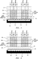
- an optical film material 10 containing refractive lenses 12 encapsulated below a layer of a thermoset polymer 14, an optical spacer 16, and image icons 18 was prepared and then embedded between a 150 micron thick base layer 20 prepared using an opaque white polycarbonate film from SABIC with the product designation Lexan SD8B24 film, and a multi-layer construction made up of three laser markable layers 22a, 22b, 22c of 150 micron thick laser markable transparent polycarbonate film from SABIC with the product designation Lexan SD8B94 film, and a 150 micron thick outerlayer 24 prepared using a clear polycarbonate film from SABIC with the product designation Lexan SD8B14 film.
- An image was then marked in the laser markable transparent polycarbonate film layers 22a, 22b, 22c using a V-Lase 10 Watt Q-switched 1064 nm laser marking system, which produced laser light emission at 30,000 Hz with a power setting of 80%, and scan speed of 200 mm/sec.
- the resulting material or device contained the laser marked image with no detectable damage to the optical film material or internal interfaces.
- an optical film material 26 containing metalized reflective lenses 28, an optical spacer 30, and image icons 32 was prepared and then embedded between a 150 micron thick Lexan SD8B24 opaque white polycarbonate film base layer 34, and a multi-layer construction made up of a 150 micron thick Lexan SD8B14 clear polycarbonate innerlayer 36, and three 150 micron thick Lexan SD8B94 laser markable transparent polycarbonate film overlayers 38a, 38b, 38c.
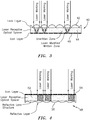
- an optical film material 40 containing refractive lenses 42, a laser markable optical spacer 44, and image icons 46 was prepared.
- the laser markable optical spacer 44 was a 50 micron thick, clear polycarbonate sheet from 3M, 3M Center, St. Paul, MN 55144-100 ("3M") under the product designation Clear LE clear polycarbonate film.
- An array of refractive lenses 42 with a 58 micron focal length were formed on an uppermost surface of the optical spacer 44, and a 3 micron thick arrangement or layer of pigmented image icons 46 was formed on the lowermost surface of the optical spacer 44.
- the prepared micro-optic film material projected synthetically magnified images with sharp focus.
- the resulting material or device contained the laser marked image with no detectable damage to the refractive lenses 42.
- the lenses were transparent enough to the 1064nm laser light to allow transmission of the laser into the laser markable optical spacer 44 without damaging the lenses 42, or introducing significant swelling or distortion of the synthetic images, yet producing indelible marking or darkening within the structure.
- an optical film material 48 containing reflective lenses 50, a laser markable optical spacer 52, and image icons 54 was prepared.
- the laser markable optical spacer 52 was a 50 micron thick, clear polycarbonate sheet from 3M, 3M Center, St. Paul, MN 55144-100 ("3M") under the product designation Clear LE clear polycarbonate film.
- An array of reflective lenses 50 with a 52 micron focal length were formed on the lowermost surface of the optical spacer 52, and a 3 micron thick arrangement or layer of pigmented image icons 54 was formed on the uppermost surface of the optical spacer 52.
- the prepared micro-optic film material projected synthetically magnified images with sharp focus.
- An image was marked in the optical spacer 52 using the same laser marking system and settings as set forth above in Example 1.
- the resulting material or device contained the laser marked image with no detectable damage to the reflective lenses 50.
- the image icons were transparent enough to the 1064nm laser light to allow transmission of the laser into the laser markable optical spacer 52 without damaging the image icons 54, or introducing significant swelling or distortion of the synthetic images, yet producing indelible marking or darkening within the structure.
- an optical film material 56 containing refractive lenses 58 encapsulated below a layer of a thermoset polymer 60, an optical spacer 62, and image icons 64 was prepared.
- a 150 micron thick laser markable transparent polycarbonate film 68 from SABIC with the product designation Lexan SD8B94 film was then applied to the underside of the thermal spacer layer 66.
- An image was marked in the laser markable film 68 using a V-Lase 10 Watt Q-switched 1064 nm laser marking system at the following settings: 30,000 Hz, 80% power, and scan speed of 200 mm/sec.
- the resulting material or device contained the laser marked image with no detectable damage to the optical film material 56, or delamination between layers of the device.
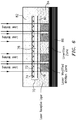
- an optical film material 70 containing refractive lenses 72 encapsulated below a layer of acrylic thermoplastic adhesive 74, an optical spacer 76, and image icons 78 was prepared.
- the optical film material 70 was backcoated with a 5 micron thick layer of acrylic adhesive 80 and then die cut into a 19 mm (0.75 inch) diameter circle.
- Above the die cut optical film material 70 was placed a layer of 150 micron thick clear polycarbonate film 82 from SABIC under the product designation Lexan SD8B14 film.
- a 150 micron thick laser markable transparent polycarbonate film 84 from SABIC with the product designation Lexan SD8B94 film was then applied to the adhesive coated underside of the optical film material 70, followed by a 150 micron thick layer of opaque white polycarbonate film 86 from SABIC with the product designation Lexan SD8B24 film.
- This construction was trimmed to a size of 89mm x 127mm, placed into a heated platen press and the layers molded together at a temperature of 177 °C (350 °F) and a pressure of 15.8 megapascals (2,286 psi) for a period of 10 minutes.
- the result was a composite card having a patch of optical film material 70 molded therein.
- An image was marked in the laser markable film 84 using a V-Lase 10 Watt Q-switched 1064 nm laser marking system at the following settings: 30,000 Hz, a scan speed of 200 mm/sec, and a power setting of 50%.
- the resulting composite card contained the laser marked image with no detectable damage to the optical film material 70, or delamination between layers of the card.
- the inventive laser markable and laser marked device may be used in the form of, for example, a sheet material for use in making, for example, banknotes, passports, and the like, or it may adopt a thicker, more robust form for use as, for example, a base platform for an ID card, high value or other security document.
- the inventive device may also be used in the form of a security strip, thread, patch, or overlay and mounted to a surface of, or at least partially embedded within a fibrous or non-fibrous sheet material (e.g ., banknote, passport, ID card, credit card, label), or commercial product ( e.g ., optical disks, CDs, DVDs, packages of medical drugs), etc., for authentication purposes.
- the base diameter of the refractive or reflective focusing elements in the optical film material is preferably less than about 50 microns, preferably from about 5 to about 30 microns, and more preferably from about 10 to about 25 microns, while the total thickness of the inventive device is preferably less than or equal to about 3 millimeters (mm) including (but not limited to) thicknesses: ranging from about 1 to about 3 mm; ranging from about 500 microns to about 1 mm; ranging from about 200 to about 500 microns, ranging from about 50 to about 199 microns, and of less than about 50 microns.
- the base diameter of the refractive or reflective focusing elements is preferably less than about 50 microns, preferably from about 5 to about 30 microns, and more preferably from about 10 to about 25 microns, while the total thickness of the inventive device is preferably less than about 50 microns (more preferably, less than about 45 microns, and most preferably, from about 10 to about 40 microns).
- the security strips, threads, patches and overlays may be partially embedded within or mounted on a surface of a document.
- portions thereof are exposed at the surface of the document at spaced intervals along the length of the strip or thread at windows or apertures in the document.
- the inventive device may be at least partially incorporated in security papers during manufacture by techniques commonly employed in the papermaking industry.
- the inventive device in the form of a strip or thread may be fed into a cylinder mold papermaking machine, cylinder vat machine, or similar machine of known type, resulting in total or partial embedment of the strip or thread within the body of the finished paper.
- the security strips, threads, patches and overlays may also be adhered or bonded to a surface of a document with or without the use of an adhesive. Bonding without the use of an adhesive may be achieved using, for example, thermal welding techniques such as heated platen press, ultrasonic welding, vibration welding, and laser fusing. Adhesives for adhering the inventive devices to a surface of a document may be one of hot melt adhesives, heat activatable adhesives, pressure sensitive adhesives, and polymeric laminating films. These adhesives are preferably crosslinkable in nature, such as UV cured acrylic or epoxy.
- the inventive device forms part of a label construction containing a transparent or translucent adhesive (i.e ., the transparent thermoplastic material layer).
- the inventive device may be placed on the inside of a package, so that the synthetic images and static 2D images remain visible.
- the base diameter of the refractive or reflective focusing elements of the optical film material is preferably less than about 50 microns, preferably from about 5 to about 30 microns, and more preferably from about 10 to about 25 microns, while the total thickness of the inventive device is preferably less than about 200 microns (more preferably, less than about 75 microns, and most preferably, from about 10 to about 50 microns).
Landscapes
- Physics & Mathematics (AREA)
- Optics & Photonics (AREA)
- Engineering & Computer Science (AREA)
- Health & Medical Sciences (AREA)
- Accounting & Taxation (AREA)
- Electromagnetism (AREA)
- General Health & Medical Sciences (AREA)
- Toxicology (AREA)
- Finance (AREA)
- Manufacturing & Machinery (AREA)
- Business, Economics & Management (AREA)
- General Physics & Mathematics (AREA)
- Computer Security & Cryptography (AREA)
- Thermal Transfer Or Thermal Recording In General (AREA)
- Credit Cards Or The Like (AREA)
- Illuminated Signs And Luminous Advertising (AREA)
- Laminated Bodies (AREA)
Claims (15)
- Verfahren zum Lasermarkieren eines oder mehrerer statischer zweidimensionaler Bilder auf oder in einer Vorrichtung, die ein optisches Filmmaterial (10, 26, 40, 48, 56, 70) verkörpert oder umfasst, wobei das Verfahren umfasst:Identifizieren einer oder mehrerer Schichten oder Grenzflächen innerhalb des optischen Filmmaterials (10, 26, 40, 48, 56, 70), die durch Laserenergie oder durch Wärme und Gas, die durch Laserabsorption innerhalb einer Laserempfangsschicht erzeugt werden, beschädigt werden können, im Folgenden als laserempfindliche Schicht oder Grenzfläche bezeichnet;entweder Positionieren einer oder mehrerer durch Laserenergie markierbarer Schichten (22a, 22b, 22c, 38a, 38b, 38c, 44, 52, 68, 84), im folgenden als lasermarkierbare Schicht (22a, 22b, 22c, 38a, 38b, 38c, 44, 52, 68, 84) bezeichnet, oberhalb der laserempfindlichen Schicht oder Grenzfläche,oder Positionieren einer oder mehrerer thermischer Abstandshalterschichten (66), die dazu dienen, das optische Filmmaterial (10, 26, 40, 48, 56, 70) von der während des Lasermarkierungsprozesses erzeugten Wärme zu isolieren, und einer oder mehrerer lasermarkierbare Schichten (68) unterhalb des optischen Filmmaterials (10, 26, 40, 48, 56, 70), wobei sich die eine oder mehreren thermischen Abstandshalterschichten (66) zwischen dem optischen Filmmaterial (10, 26, 40, 48, 56, 70) und der einen oder mehreren lasermarkierbaren Schichten (68) befinden,oder Modifizieren der laserempfindlichen Grenzfläche, um die Haftfestigkeit und/oder den thermischen Widerstand der Grenzfläche zu erhöhen,oder Ersetzen der laserempfindlichen Schicht durch eine Schicht aus einem Material mit einer höheren Bindungsstärke und/oder einer höheren Wärmebeständigkeit;Belichten der Vorrichtung mit Laserenergie, um so ein oder mehrere statisch zweidimensionale Bilder auf oder in der einen oder den mehreren lasermarkierbaren Schichten (22a, 22b, 22c, 38a, 38b, 38c, 44, 52, 68, 84) zu markieren,dadurch gekennzeichnet, dassdas optische Filmmaterial (10, 26, 40, 48, 56, 70) mindestens ein synthetisch vergrößertes Bild projiziert.
- Verfahren nach Anspruch 1, weiterhin umfassend das Ausformen der Schichten zusammen unter Verwendung von Wärme und Druck, um eine Vorrichtung auszubilden, die das optische Filmmaterial (10, 26, 40, 48, 56, 70) enthält, ausgeführt vor dem Belichten der Vorrichtung mit Laserenergie oder dem Verfahren nach Anspruch 1, wobei eine oder mehrere lasermarkierbare Schichten (22a, 22b, 22c, 38a, 38b, 38c, 44, 52, 84) über der laserempfindlichen Schicht positioniert werden;
wobei das optische Filmmaterial (10, 26, 40, 48, 56, 70) wahlweise aus einer oder mehreren wahlweise eingekapselten Anordnungen von refraktiven fokussierenden Elementen (12, 42, 58, 72) und einer oder mehreren Anordnungen von Bildsymbolen (18, 32, 46, 54, 64, 78) besteht, die auf gegenüberliegenden Seiten einer optischen Abstandshalterschicht angeordnet sind, wobei die eine oder die mehreren Anordnungen von Bildsymbolen (18, 32, 46, 54, 64, 78) die eine oder die mehreren Schichten innerhalb des optischen Filmmaterials (10, 26, 40, 48, 56, 70) bilden, die durch Laserenergie beschädigt werden können, oder das optische Filmmaterial (10, 26, 40, 48, 56, 70) aus einer oder mehreren wahlweise eingekapselten Anordnungen von reflektierenden fokussierenden Elementen (28, 50) und einer oder mehreren Anordnungen von Bildsymbolen (18, 32, 46, 54, 64, 78) besteht, die auf gegenüberliegenden Seiten einer optischen Abstandshalterschicht angeordnet sind, wobei die eine oder die mehreren wahlweise eingekapselten Anordnungen reflektierender fokussierender Elemente (28, 50) die eine oder mehreren Schichten innerhalb des optischen Filmmaterials (10, 26, 40, 48, 56, 70) bilden, die durch Laserenergie beschädigt werden können, oder die Vorrichtung mit einer Laserenergie belichtet wird, die ausreicht, um eine lesbare Markierung innerhalb einer lasermarkierbaren Schicht (22a, 22b, 22c, 38a, 38b, 38c, 44, 52, 84) zu erzeugen. - Verfahren nach Anspruch 1, bei dem die eine oder die mehreren mit Laserenergie markierbaren Schichten (22a, 22b, 22c, 38a, 38b, 38c, 44, 52, 84) unter Verwendung von thermoplastischen Polymeren vorbereitet werden, die aus der Gruppe von Polyethersulfon, Polysulfon, Polycarbonat und Polyphenylensulfid gewählt sind,
wobei wahlweise die eine oder die mehreren Schichten (22a, 22b, 22c, 38a, 38b, 38c, 44, 52, 84), die durch Laserenergie markierbar sind, lasermarkierbare transparente Polycarbonatfilme sind oder die eine oder mehreren Schichten (22a, 22b, 22c, 38a, 38b, 38c, 44, 52, 84), die durch Laserenergie markierbar sind, lasermarkierbare klare Polycarbonatblätter sind. - Verfahren nach Anspruch 1, bei dem die eine oder die mehreren Schichten (22a, 22b, 22c, 38a, 38b, 38c, 44, 52, 84), die durch Laserenergie markierbar sind, unter Verwendung von einem oder mehreren Laseradditiven und einem oder mehreren thermoplastischen Polymeren hergestellt werden, die aus der Gruppe von Polystyren, Styren-Acrylnitril, Acrylnitril-Butadien-Styren, Polyethylenterephthalat, glykolmodifiziertem Polyethylenterephthalat, Polybutylenterephthalat und Polyethylen gewählt sind, wobei gegebenenfalls der eine oder die mehreren Laseradditive Ruß enthalten.
- Verfahren nach Anspruch 1, bei dem eine oder mehrere thermische Abstandshalterschichten und eine oder mehrere lasermarkierbare Schichten (22a, 22b, 22c, 38a, 38b, 38c, 44, 52, 84) unter dem optischen Filmmaterial (10, 26, 40, 48, 56, 70) angeordnet werden, wobei die eine oder die mehreren thermischen Abstandshalterschichten zwischen dem optischen Filmmaterial (10, 26, 40, 48, 56, 70) und den einen oder mehreren lasermarkierbaren Schichten (22a, 22b, 22c, 38a, 38b, 38c, 44, 52, 84) angeordnet sind,
wobei wahlweise das optische Filmmaterial (10, 26, 40, 48, 56, 70) eine Anordnung von eingekapselten refraktiven fokussierenden Elementen (12, 42, 58, 72) und eine Anordnung von Bildsymbolen (18, 32, 46, 54, 64, 78) umfasst, die durch eine optische Abstandshalterschicht getrennt sind, oder die eine oder mehreren thermischen Abstandshalterschichten unter Verwendung eines klaren thermoplastischen Materials vorbereitet werden oder die eine oder mehreren thermischen Abstandshalterschichten eine Dicke im Bereich von etwa 5 bis etwa 500 Mikrometer haben oder die Vorrichtung einer Laserenergie ausgesetzt wird, die ausreicht, um eine lesbare Markierung innerhalb einer lasermarkierbaren Schicht (22a, 22b, 22c, 38a, 38b, 38c, 44, 52, 84) zu erzeugen. - Lasermarkierbare optische Vorrichtung, die umfasst:ein optisches Filmmaterial (10, 26, 40, 48, 56, 70), das eine oder mehrere Anordnungen von Fokussierelementen (12, 28, 42, 50, 58, 72) und eine oder mehrere Anordnungen von Bildsymbolen (18, 32, 46, 54, 64, 78) umfasst, die auf gegenüberliegenden Seiten einer optischen Abstandshalterschicht angeordnet sind, wobei wenigstens ein Abschnitt der Fokussierelemente (12, 28, 42, 50, 58, 72) wenigstens ein synthetisch vergrößertes Bild von wenigstens einem Abschnitt der Bildsymbole (18, 32, 46, 54, 64, 78) ausbildet; undwenigstens eine Anordnung oder Schicht innerhalb oder eine Schicht oberhalb oder unterhalb des optischen Filmmaterials (10, 26, 40, 48, 56, 70) durch Laserenergie markierbar ist, unddie eine oder die mehreren lasermarkierbaren Anordnungen oder Schichten (22a, 22b, 22c, 38a, 38b, 38c, 44, 52, 84) dazu eingerichtet sind, statische zweidimensionale Bilder zu haben, die auf oder in ihnen lasermarkiert sind, ohne die Fokussierelemente (12, 28, 42, 50, 58, 72) oder die Bildsymbole (18, 32, 46, 54, 64, 78) des optischen Filmmaterials (10, 26, 40, 48, 56, 70) zu beschädigen.
- Lasermarkierbare optische Vorrichtung nach Anspruch 6, bei der die eine oder mehreren Anordnungen von Fokussierelementen (12, 28, 42, 50, 58, 72) eingekapselt sind und/oder die lasermarkierbare optische Vorrichtung weiterhin eine oder mehrere Schichten oberhalb und/oder unterhalb des optischen Filmmaterials umfasst, und/oder das optische Filmmaterial (10, 26, 40, 48, 56, 70) eine wahlweise eingekapselte Anordnung von refraktiven Fokussierelementen (12, 42, 58, 72) und eine Anordnung von Bildsymbolen (18, 32, 46, 54, 64, 78) umfasst, die durch eine optische Abstandshalterschicht getrennt sind, wobei eine oder mehrere Anordnungen oder Schichten, die oberhalb der Anordnung der Bildsymbole (18, 32, 46, 54, 64, 78) angeordnet sind, eine lasermarkierbare Anordnung oder Schicht (22a, 22b, 22c, 38a, 38b, 38c, 44, 52, 84) sind.
- Lasermarkierbare optische Vorrichtung nach Anspruch 6, bei der eine oder mehrere Schichten oberhalb und/oder unterhalb des optischen Filmmaterials (10, 26, 40, 48, 56, 70) angeordnet sind und
die eine oder die mehreren Schichten oberhalb und/oder unterhalb des optischen Filmmaterials (10, 26, 40, 48, 56, 70) eine oder mehrere transparente thermoplastische Materialschichten umfassen, die dazu dienen, eine gewünschte Gesamtdicke der Vorrichtung zu erreichen, oder wenn sie als eine äußerste Schicht positioniert sind, dem Gerät einen erhöhten Widerstand gegen Manipulation oder Veränderung und Verschleiß verleihen,
oder
das optische Filmmaterial (10, 26, 40, 48, 56, 70) eine Anordnung von eingekapselten refraktiven fokussierenden Elementen (12, 42, 58, 72) und eine Anordnung von Bildsymbolen (18, 32, 46, 54, 64, 78) umfasst, die durch eine optische Abstandshalterschicht getrennt sind, wobei eine oder mehrere Anordnungen oder Schichten, die sich oberhalb der Anordnung von Bildsymbolen (18, 32, 46, 54, 64, 78) befinden, eine lasermarkierbare Anordnung oder Schicht (22a, 22b, 22c, 38a, 38b, 38c, 44, 52, 84) sind,
wobei wahlweise eine äußerste Schicht, die über dem optischen Filmmaterial (10, 26, 40, 48, 56, 70) angeordnet ist, eine transparente thermoplastische Materialschicht ist, wobei wahlweise die transparente thermoplastische Materialschicht eine Dicke im Bereich von etwa 5 bis etwa 500 Mikrometer aufweist,
oder
wahlweise die refraktiven fokussierenden Elemente (12, 42, 58, 72) unter Verwendung eines Materials mit einem Brechungsindex eingekapselt sind, der im Wesentlichen oder messbar verschieden ist von dem Brechungsindex des Materials, das zur Ausbildung der fokussierenden Elemente verwendet wird,
wobei wahlweise die Differenz der Brechungsindizes bewirkt, dass die Brennweite der Fokussierelemente auf die eine oder die mehreren Anordnungen von Bildsymbolen (18, 32, 46, 54, 64, 78) konvergiert.
oder
wahlweise das Einkapselungsmaterial transparent, transluzent, getönt oder pigmentiert ist und wahlweise zusätzliche Funktionalität für Sicherheits- und Authentifizierungszwecke bereitstellt, die Unterstützung von automatisierten Systemen zur Authentifizierung, Verifizierung, Verfolgung, Zählung und Erfassung von Währungen umfasst, die auf optische Effekte, elektrische Leitfähigkeit oder elektrische Kapazität und Magnetfelderfassung zurückgreifen, wobei das Einkapselungsmaterial wahlweise aus der Gruppe der Haftmittel, Gele, Klebstoffe, Lacke, Flüssigkeiten, ausgeformten Polymeren und Polymeren oder anderen Materialien gewählt ist, die organische oder metallische Dispersionen enthalten, vorausgesetzt, dass die Lichtbrechung nicht vollständig unterbrochen ist. - Lasermarkierbare optische Vorrichtung nach Anspruch 6, bei der das optische Filmmaterial (10, 26, 40, 48, 56, 70) eine wahlweise eingekapselte Anordnung reflektierender fokussierender Elemente (28, 50) und eine Anordnung von Bildsymbolen (18, 32, 46, 54, 64, 78) umfasst, die durch eine optische Abstandshalterschicht getrennt sind, wobei eine oder mehrere Anordnungen oder Schichten, die sich oberhalb der wahlweise eingekapselten Anordnung reflektierender Fokussierelemente (28, 50) befinden, eine lasermarkierbare Anordnung oder Schicht (22a, 22b, 22c, 38a, 38b, 38c, 44, 52, 84) sind,
wobei wahlweise die reflektierenden Fokussierelemente (28, 50) metallisiert oder mit einem nicht-metallischen Material mit hohem Brechungsindex beschichtet sind, wobei wahlweise die reflektierenden Fokussierelemente (28, 50) mit einem nicht-metallischen Material mit hohem Brechungsindex beschichtet sind, das aus der Gruppe gewählt ist, die aus Zinksulfid, Indiumzinnoxid und Kombinationen davon besteht. - Lasermarkierbare optische Vorrichtung nach Anspruch 6, die eine selbständige Vorrichtung ist, die ein optisches Filmmaterial (10, 26, 40, 48, 56, 70) umfasst, das eine wahlweise eingekapselte Anordnung von refraktiven oder reflektierenden Fokussierelementen (28, 50) und eine Anordnung von Bildsymbolen (18, 32, 46, 54, 64, 78) aufweist, die durch eine lasermarkierbare optische Abstandshalterschicht (44, 52) getrennt sind.
- Lasermarkierbare optische Vorrichtung nach Anspruch 6, bei der die eine oder die mehreren Anordnungen oder Schichten (22a, 22b, 22c, 38a, 38b, 38c, 44, 52, 84), die durch Laserenergie markierbar sind, unter Verwendung von thermoplastischen Polymeren vorbereitet werden, die aus der Gruppe aus Polyethersulfon, Polysulfon, Polycarbonat und Polyphenylensulfid gewählt sind,
wobei wahlweise die eine oder die mehreren Schichten (22a, 22b, 22c, 38a, 38b, 38c, 44, 52, 84), die durch Laserenergie markierbar sind, lasermarkierbare transparente Polycarbonatfilme sind, oder die eine oder die mehreren Schichten (22a, 22b, 22c, 38a, 38b, 38c, 44, 52, 84), die durch Laserenergie markierbar sind, lasermarkierbare klare Polycarbonatblätter sind. - Lasermarkierbare optische Vorrichtung nach Anspruch 6, bei der die eine oder mehreren Schichten (22a, 22b, 22c, 38a, 38b, 38c, 44, 52, 84), die durch Laserenergie markierbar sind, unter Verwendung eines oder mehrerer Laseradditive und eines oder mehrerer thermoplastischer Polymere hergetsellt werden, die aus der Gruppe gewählt sind, die aus Polystyren, Styrenacrylnitril, Acrylnitril-Butadien-Styren, Polyethylenterephthalat, glykolmodifiziertem Polyethylenterephthalat, Polybutylenterephthalat und Polyethylen besteht,
wobei wahlweise das eine oder die mehreren Laseradditive Ruß enthalten. - Lasermarkierbare optische Vorrichtung nach Anspruch 6, die aus dem optischen Filmmaterial (10, 26, 40, 48, 56, 70), einer oder mehreren darunterliegenden lasermarkierbaren Schichten (22a, 22b, 22c, 38a, 38b, 38c, 44, 52, 84) und einer oder mehreren thermischen Abstandshalterschichten besteht, die zwischen dem optischen Filmmaterial (10, 26, 40, 48, 56, 70) und der einen oder mehreren darunter liegenden lasermarkierbaren Schichten (22a, 22b, 22c, 38a, 38b, 38c, 44, 52, 84) besteht,
wobei wahlweise das optische Filmmaterial (10, 26, 40, 48, 56, 70) eine Anordnung von eingekapselten refraktiven fokussierenden Elementen (12, 42, 58, 72) und eine Anordnung von Bildsymbolen (18, 32, 46, 54, 64, 78) umfasst, die durch eine optische Abstandshalterschicht getrennt sind, oder die eine oder mehreren thermischen Abstandshalterschichten unter Verwendung eines klaren thermoplastischen Materials vorbereitet werden, oder die eine oder mehreren thermischen Abstandshalterschichten eine Dicke im Bereich von etwa 5 bis etwa 500 Mikrometer haben. - Lasermarkierte optische Vorrichtung, die aus der lasermarkierbaren optischen Vorrichtung nach Anspruch 6 angefertigt ist, wobei die eine oder mehreren lasermarkierbaren Anordnungen oder Schichten (22a, 22b, 22c, 38a, 38b, 38c, 44, 52, 84) ein oder mehrere lasermarkierte statische zweidimensionale Bilder darauf aufweisen.
- Blattmaterial oder Basisplattform, die aus der lasermarkierbaren optischen Vorrichtung nach Anspruch 6 oder der lasermarkierten optischen Vorrichtung nach Anspruch 14 hergestellt ist, oder Dokument, das aus dem Blattmaterial oder der Basisplattform hergestellt ist.
Applications Claiming Priority (2)
| Application Number | Priority Date | Filing Date | Title |
|---|---|---|---|
| US201161437157P | 2011-01-28 | 2011-01-28 | |
| PCT/US2012/022912 WO2012103441A1 (en) | 2011-01-28 | 2012-01-27 | A laser marked device |
Publications (2)
| Publication Number | Publication Date |
|---|---|
| EP2668526A1 EP2668526A1 (de) | 2013-12-04 |
| EP2668526B1 true EP2668526B1 (de) | 2018-07-04 |
Family
ID=45976502
Family Applications (1)
| Application Number | Title | Priority Date | Filing Date |
|---|---|---|---|
| EP12715241.1A Active EP2668526B1 (de) | 2011-01-28 | 2012-01-27 | Lasermarkierte vorrichtung |
Country Status (12)
| Country | Link |
|---|---|
| US (2) | US8755121B2 (de) |
| EP (1) | EP2668526B1 (de) |
| JP (1) | JP6042347B2 (de) |
| KR (1) | KR102012526B1 (de) |
| CN (1) | CN103477250B (de) |
| AU (1) | AU2012211170B2 (de) |
| BR (1) | BR112013018970A2 (de) |
| CA (1) | CA2825655C (de) |
| MX (1) | MX2013008593A (de) |
| MY (1) | MY159709A (de) |
| RU (1) | RU2614643C9 (de) |
| WO (1) | WO2012103441A1 (de) |
Families Citing this family (56)
| Publication number | Priority date | Publication date | Assignee | Title |
|---|---|---|---|---|
| US9542635B2 (en) | 2007-12-31 | 2017-01-10 | Composecure, Llc | Foil composite card |
| IN2014CN02023A (de) | 2011-08-19 | 2015-05-29 | Visual Physics Llc | |
| JP6053932B2 (ja) | 2012-08-17 | 2016-12-27 | ビジュアル フィジクス エルエルシー | 微細構造を最終基板に転写するプロセス |
| DK2956310T3 (da) | 2013-02-13 | 2019-10-14 | Composecure Llc | Holdbart kort |
| RU2673137C9 (ru) | 2013-03-15 | 2019-04-04 | Визуал Физикс, Ллс | Оптическое защитное устройство |
| US9873281B2 (en) | 2013-06-13 | 2018-01-23 | Visual Physics, Llc | Single layer image projection film |
| DE102013108485B4 (de) | 2013-08-06 | 2015-06-25 | Khs Gmbh | Vorrichtung und Verfahren zum Fehlertracking bei Bandmaterialien |
| RU2555500C1 (ru) * | 2014-02-28 | 2015-07-10 | Сергей Николаевич Максимовский | Способ создания цветного защитного изображения внутри листового материала, видимого в проходящем свете и отображенного на лицевой и оборотной поверхностях этого материала совокупностью соосных входных отверстий, и листовой материал для его реализации |
| CA2943987A1 (en) | 2014-03-27 | 2015-10-01 | Visual Physics, Llc | An optical device that produces flicker-like optical effects |
| US10766292B2 (en) | 2014-03-27 | 2020-09-08 | Crane & Co., Inc. | Optical device that provides flicker-like optical effects |
| DE102014004700A1 (de) * | 2014-03-31 | 2015-10-01 | Giesecke & Devrient Gmbh | Sicherheitselement mit einem Linsenrasterbild |
| JP6680767B2 (ja) | 2014-05-22 | 2020-04-15 | コンポーズキュア,リミティド ライアビリティ カンパニー | 選択された質感と色を有する取引及びidカード |
| MX2017000283A (es) * | 2014-07-08 | 2017-04-10 | Xyleco Inc | Marcado de productos a base de plastico. |
| CA3168669C (en) * | 2014-07-17 | 2024-04-09 | Visual Physics, Llc | An improved polymeric sheet material for use in making polymeric security documents such as banknotes |
| KR102497982B1 (ko) | 2014-09-16 | 2023-02-09 | 크레인 시큐리티 테크놀로지스, 인크. | 보안 렌즈 층 |
| US9922935B2 (en) * | 2014-09-17 | 2018-03-20 | Samsung Electronics Co., Ltd. | Semiconductor package and method of fabricating the same |
| DE102014013917A1 (de) * | 2014-09-18 | 2016-03-24 | Giesecke & Devrient Gmbh | Sicherheitsdokument mit Schutzschicht |
| WO2016065331A2 (en) | 2014-10-24 | 2016-04-28 | Wavefront Technology, Inc. | Optical products, masters for fabricating optical products, and methods for manufacturing masters and optical products |
| US10783422B2 (en) | 2014-11-03 | 2020-09-22 | Composecure, Llc | Ceramic-containing and ceramic composite transaction cards |
| EP3037274B1 (de) * | 2014-12-22 | 2018-11-21 | Agfa-Gevaert | Lasermarkierbare Sicherheitsartikel und Dokumente und Verfahren zur Herstellung von Bildern in solchen Sicherheitsartikeln |
| US10189292B2 (en) | 2015-02-11 | 2019-01-29 | Crane & Co., Inc. | Method for the surface application of a security device to a substrate |
| EP3795367A1 (de) | 2015-07-13 | 2021-03-24 | Wavefront Technology, Inc. | Optische produkte |
| US20170057275A1 (en) * | 2015-08-27 | 2017-03-02 | Crane Security Technologies, Inc. | Single or dual transfer process for preparing and transferring sharply defined single elements to objects to be protected |
| WO2017184581A1 (en) | 2016-04-22 | 2017-10-26 | Wavefront Technology, Inc. | Optical switch devices |
| US10864762B2 (en) | 2016-08-15 | 2020-12-15 | Visual Physics, Llc | Anti-harvestable security feature |
| CN109641317B (zh) | 2016-08-19 | 2021-08-06 | 利惠商业有限公司 | 服装的激光整理 |
| AU2017321840B2 (en) | 2016-09-05 | 2021-12-09 | Toppan Printing Co., Ltd. | Information display medium and manufacturing method relating thereto |
| DE102016012625A1 (de) * | 2016-10-21 | 2018-04-26 | Giesecke+Devrient Currency Technology Gmbh | Sicherheitselement und Verfahren zum Herstellen eines Sicherheitselements |
| RU2634571C1 (ru) * | 2016-10-24 | 2017-10-31 | Сергей Николаевич Максимовский | Способ создания оригинального цветного защитного изображения внутри листового материала |
| DE102016015015A1 (de) * | 2016-12-15 | 2018-06-21 | Giesecke+Devrient Currency Technology Gmbh | Verfahren zum Herstellen eines Sicherheitselements mit einem Linsenrasterbild |
| ES2922024T3 (es) | 2017-02-10 | 2022-09-06 | Crane & Co Inc | Dispositivo óptico de seguridad legible por máquina |
| DE102017112076A1 (de) * | 2017-06-01 | 2018-12-06 | Osram Opto Semiconductors Gmbh | Optoelektronisches bauelement und verfahren zum herstellen eines optoelektronischen bauelements |
| CA3062579A1 (en) * | 2017-06-05 | 2018-12-13 | Crane & Co., Inc. | An optical device that provides flicker-like optical effects |
| DE102017005779A1 (de) * | 2017-06-19 | 2018-12-20 | Giesecke+Devrient Mobile Security Gmbh | Mikrooptisches Element mit Farbwechsel |
| AU2017101215B4 (en) * | 2017-09-05 | 2018-03-15 | Ccl Secure Pty Ltd | Laser marking and/or ablation to create micro-imagery for micro-lens security features |
| GB2584552B (en) * | 2017-10-19 | 2021-07-21 | De La Rue Int Ltd | Security devices, security articles, security documents and methods for their manufacture |
| WO2019077419A1 (en) | 2017-10-20 | 2019-04-25 | Wavefront Technology, Inc. | OPTICAL SWITCH DEVICES |
| CN111565880B (zh) | 2017-10-31 | 2022-09-23 | 利惠商业有限公司 | 激光精加工设计工具 |
| EP3704608A4 (de) | 2017-10-31 | 2021-08-18 | Levi Strauss & Co. | Verwendung von neuronalen netzen beim entwurf von kleidung |
| CA3087414A1 (en) | 2018-01-03 | 2019-07-11 | Visual Physics, Llc | Micro-optic security device with interactive dynamic security features |
| RU2674691C1 (ru) * | 2018-02-08 | 2018-12-12 | Сергей Николаевич Максимовский | Способ создания в тонком листовом материале скрытого изображения из множества пар объёмных наноструктур для защиты от подделки ценных бумаг и идентификационных документов несколькими публичными признаками |
| US11026461B2 (en) | 2018-02-27 | 2021-06-08 | Levi Strauss & Co. | Substituting an existing collection in an apparel management system |
| US11352738B2 (en) | 2018-02-27 | 2022-06-07 | Levi Strauss & Co. | On-demand manufacturing of apparel by laser finishing fabric rolls |
| CN108510007A (zh) * | 2018-04-08 | 2018-09-07 | 北京知道创宇信息技术有限公司 | 一种网页篡改检测方法、装置、电子设备及存储介质 |
| JP2021529688A (ja) | 2018-07-03 | 2021-11-04 | クレイン アンド カンパニー、 インコーポレイテッド | 向上されたハーベスティング耐性を示すセキュリティデバイスが取り付けられたセキュリティ文書 |
| US10793998B2 (en) | 2018-08-07 | 2020-10-06 | Levi Strauss & Co. | Outdoor retail space structure |
| US11484080B2 (en) | 2018-11-30 | 2022-11-01 | Levi Strauss & Co. | Shadow neutral 3-D garment rendering |
| WO2020214239A1 (en) | 2019-04-19 | 2020-10-22 | Wavefront Technology, Inc. | Optical switch devices |
| KR102105081B1 (ko) * | 2019-05-03 | 2020-04-27 | 지제이엠 주식회사 | 초점 거리를 사용하여 다양한 두께로 제작이 가능한 패턴 라벨 |
| CN110337193A (zh) * | 2019-05-05 | 2019-10-15 | 天津光韵达光电科技有限公司 | 一种smt激光模板的mark点及其加工方法 |
| CN114423896A (zh) | 2019-07-23 | 2022-04-29 | 利惠商业有限公司 | 对激光精加工服装的三维渲染预览 |
| US11685180B2 (en) * | 2019-08-19 | 2023-06-27 | Crane & Co., Inc. | Micro-optic security device with zones of color |
| US11587469B2 (en) | 2019-09-24 | 2023-02-21 | Rockwell Automation Technologies, Inc. | Indicators for industrial devices |
| JP2023508016A (ja) * | 2019-12-18 | 2023-02-28 | クレイン アンド カンパニー、 インコーポレイテッド | 位相合わせされた画像層を有するマイクロ光学セキュリティデバイス |
| CN114518660B (zh) * | 2020-11-19 | 2024-09-06 | 京东方科技集团股份有限公司 | 一种裸眼3d器件的制备方法、裸眼3d器件 |
| JP6990760B1 (ja) | 2020-12-08 | 2022-01-12 | 住友化学株式会社 | マーク付き光学積層体、及び、マーク付き光学積層体の製造方法 |
Citations (1)
| Publication number | Priority date | Publication date | Assignee | Title |
|---|---|---|---|---|
| US20050247794A1 (en) * | 2004-03-26 | 2005-11-10 | Jones Robert L | Identification document having intrusion resistance |
Family Cites Families (244)
| Publication number | Priority date | Publication date | Assignee | Title |
|---|---|---|---|---|
| US992151A (en) | 1909-02-04 | 1911-05-16 | Rodolphe Berthon | Apparatus for color photography. |
| US1824353A (en) | 1926-12-15 | 1931-09-22 | Jensen Rasmus Olaf Jonas | Screen for showing projected images in lighted rooms and for shortexposure photography |
| US1849036A (en) | 1926-12-23 | 1932-03-08 | Victor C Ernst | Photographic process and auxiliary element therefor |
| US1942841A (en) | 1931-01-19 | 1934-01-09 | Shimizu Takeo | Daylight screen |
| US2268351A (en) | 1938-08-25 | 1941-12-30 | Tanaka Nawokich | Means for presenting pictures in apparent three dimensions |
| US2355902A (en) | 1941-04-10 | 1944-08-15 | Photoplating Company | Sign with animated effect |
| US2432896A (en) | 1945-03-12 | 1947-12-16 | Hotchner Fred | Retroreflective animation display |
| NL201432A (de) | 1955-03-29 | |||
| US2888855A (en) | 1956-08-23 | 1959-06-02 | Tanaka Nawokich | Means for presenting pictures in three dimensional effect |
| US3122853A (en) | 1961-08-10 | 1964-03-03 | John C Koonz | Fishing lure |
| US3264164A (en) | 1962-04-30 | 1966-08-02 | Toscony Inc | Color dynamic, three-dimensional flexible film and method of making it |
| US3241429A (en) | 1962-05-14 | 1966-03-22 | Pid Corp | Pictorial parallax panoramagram units |
| US3357772A (en) | 1963-02-27 | 1967-12-12 | Rowland Products Inc | Phased lenticular sheets for optical effects |
| GB1095286A (en) | 1963-07-08 | 1967-12-13 | Portals Ltd | Security device for use in security papers |
| US3312006A (en) | 1964-03-11 | 1967-04-04 | Rowland Products Inc | Motion displays |
| JPS414953Y1 (de) | 1964-07-28 | 1966-03-18 | ||
| JPS4622600Y1 (de) | 1965-07-02 | 1971-08-05 | ||
| US3463581A (en) | 1966-01-17 | 1969-08-26 | Intermountain Res & Eng | System for three-dimensional panoramic static-image motion pictures |
| US3811213A (en) | 1968-11-17 | 1974-05-21 | Photo Motion Corp | Moire motion illusion apparatus and method |
| JPS4941718B1 (de) | 1968-12-30 | 1974-11-11 | ||
| US3643361A (en) | 1969-11-17 | 1972-02-22 | Photo Motion Corp | Moire motion illusion apparatus |
| BE789941A (fr) | 1971-04-21 | 1973-02-01 | Waly Adnan | Systeme d'enregistrement et de lecture d'images miniaturisees |
| US3887742A (en) | 1972-04-13 | 1975-06-03 | Richard E Reinnagel | Copy resistant documents |
| US4025673A (en) | 1972-04-13 | 1977-05-24 | Reinnagel Richard E | Method of forming copy resistant documents by forming an orderly array of fibers extending upward from a surface, coating the fibers and printing the coated fibers and the copy resistant document resulting from said method |
| US3801183A (en) | 1973-06-01 | 1974-04-02 | Minnesota Mining & Mfg | Retro-reflective film |
| US4105318A (en) | 1974-05-30 | 1978-08-08 | Izon Corporation | Pinhole microfiche recorder and viewer |
| US4082426A (en) | 1976-11-26 | 1978-04-04 | Minnesota Mining And Manufacturing Company | Retroreflective sheeting with retroreflective markings |
| US4185191A (en) | 1978-06-05 | 1980-01-22 | Honeywell Inc. | Range determination system |
| US4498736A (en) | 1981-02-02 | 1985-02-12 | Griffin Robert B | Method and apparatus for producing visual patterns with lenticular sheets |
| US4892385A (en) | 1981-02-19 | 1990-01-09 | General Electric Company | Sheet-material authenticated item with reflective-diffractive authenticating device |
| US4417784A (en) | 1981-02-19 | 1983-11-29 | Rca Corporation | Multiple image encoding using surface relief structures as authenticating device for sheet-material authenticated item |
| US4345833A (en) | 1981-02-23 | 1982-08-24 | American Optical Corporation | Lens array |
| US4519632A (en) | 1982-03-19 | 1985-05-28 | Computer Identification Systems, Inc. | Identification card with heat reactive coating |
| DE3211102A1 (de) | 1982-03-25 | 1983-10-06 | Schwarz Klaus Billett Automat | Verfahren zur echtheitskontrolle von papierabschnitten und verwendung eines hierzu geeigneten farbreaktionssystems |
| JPS58175091A (ja) | 1982-04-06 | 1983-10-14 | 株式会社東芝 | セキユリテイ・ストレツド検出装置 |
| US4814594A (en) | 1982-11-22 | 1989-03-21 | Drexler Technology Corporation | Updatable micrographic pocket data card |
| US4645301A (en) | 1983-02-07 | 1987-02-24 | Minnesota Mining And Manufacturing Company | Transparent sheet containing authenticating image and method of making same |
| US4634220A (en) | 1983-02-07 | 1987-01-06 | Minnesota Mining And Manufacturing Company | Directionally imaged sheeting |
| US4507349A (en) | 1983-05-16 | 1985-03-26 | Howard A. Fromson | Security medium and secure articles and methods of making same |
| NL8400868A (nl) | 1984-03-19 | 1984-10-01 | Philips Nv | Gelaagde optische component. |
| US4534398A (en) | 1984-04-30 | 1985-08-13 | Crane & Co. | Security paper |
| US4688894A (en) | 1985-05-13 | 1987-08-25 | Minnesota Mining And Manufacturing Company | Transparent retroreflective sheets containing directional images and method for forming the same |
| US4662651A (en) | 1985-05-31 | 1987-05-05 | The Standard Register Company | Document protection using multicolor characters |
| ES2038119T3 (es) | 1985-10-15 | 1993-07-16 | Gao Gesellschaft Fur Automation Und Organisation Mbh | Soporte de datos con caracteristica optica de autenticidad, asi como procedimiento para la fabricacion y comprobacion de dicho soporte de datos. |
| US4935335A (en) | 1986-01-06 | 1990-06-19 | Dennison Manufacturing Company | Multiple imaging |
| US4920039A (en) | 1986-01-06 | 1990-04-24 | Dennison Manufacturing Company | Multiple imaging |
| DE3609090A1 (de) | 1986-03-18 | 1987-09-24 | Gao Ges Automation Org | Wertpapier mit darin eingelagertem sicherheitsfaden und verfahren zur herstellung derselben |
| CH670904A5 (de) | 1986-07-10 | 1989-07-14 | Landis & Gyr Ag | |
| JPS6464145A (en) * | 1987-09-03 | 1989-03-10 | Matsushita Electric Ind Co Ltd | Information carrier disk |
| DE3741179A1 (de) | 1987-12-04 | 1989-06-15 | Gao Ges Automation Org | Dokument mit faelschungssicherem oberflaechenrelief und verfahren zur herstellung desselben |
| IN173621B (de) | 1987-12-04 | 1994-06-18 | Portals Ltd | |
| ES2095872T5 (es) | 1989-01-31 | 2005-03-16 | Dai Nippon Insatsu Kabushiki Kaisha | Soporte de registro para transferencia termica. |
| JPH0355501A (ja) | 1989-07-25 | 1991-03-11 | Nippon Sheet Glass Co Ltd | レンズアレイ板 |
| US5085514A (en) | 1989-08-29 | 1992-02-04 | American Bank Note Holographics, Inc. | Technique of forming a separate information bearing printed pattern on replicas of a hologram or other surface relief diffraction pattern |
| US4988151A (en) | 1989-08-31 | 1991-01-29 | Hughes Aircraft Company | Method for making edge faded holograms |
| US5695346A (en) | 1989-12-07 | 1997-12-09 | Yoshi Sekiguchi | Process and display with moveable images |
| US5142383A (en) | 1990-01-25 | 1992-08-25 | American Banknote Holographics, Inc. | Holograms with discontinuous metallization including alpha-numeric shapes |
| US5044707A (en) | 1990-01-25 | 1991-09-03 | American Bank Note Holographics, Inc. | Holograms with discontinuous metallization including alpha-numeric shapes |
| US6724536B2 (en) | 1990-05-18 | 2004-04-20 | University Of Arkansas | Directional image lenticular window sheet |
| US6870681B1 (en) | 1992-09-21 | 2005-03-22 | University Of Arkansas, N.A. | Directional image transmission sheet and method of making same |
| US5232764A (en) | 1990-06-04 | 1993-08-03 | Meiwa Gravure Co., Ltd. | Synthetic resin pattern sheet |
| US5135262A (en) | 1990-06-20 | 1992-08-04 | Alcan International Limited | Method of making color change devices activatable by bending and product thereof |
| US5215864A (en) | 1990-09-28 | 1993-06-01 | Laser Color Marking, Incorporated | Method and apparatus for multi-color laser engraving |
| US5254390B1 (en) | 1990-11-15 | 1999-05-18 | Minnesota Mining & Mfg | Plano-convex base sheet for retroreflective articles |
| JP3120401B2 (ja) | 1991-01-08 | 2000-12-25 | 日本ビクター株式会社 | 光カード |
| GB9106128D0 (en) | 1991-03-22 | 1991-05-08 | Amblehurst Ltd | Article |
| GB9113462D0 (en) | 1991-06-21 | 1991-08-07 | Pizzanelli David J | Laser-activated bar-code holograms and bar-code recognition system |
| US5384861A (en) | 1991-06-24 | 1995-01-24 | Picker International, Inc. | Multi-parameter image display with real time interpolation |
| US5211424A (en) | 1991-08-15 | 1993-05-18 | Prc Inc. | Secure passport document and method of making the same |
| US5538753A (en) | 1991-10-14 | 1996-07-23 | Landis & Gyr Betriebs Ag | Security element |
| US5626969A (en) | 1992-02-21 | 1997-05-06 | General Binding Corporation | Method of manufacturing film for lamination |
| DK95292D0 (da) | 1992-07-23 | 1992-07-23 | Frithioff Johansen | Fremgangsmaade og visning til tilvejebringelse af et forstoerret billede af et todimensionalt periodisk billedmoenster |
| US5359454A (en) | 1992-08-18 | 1994-10-25 | Applied Physics Research, L.P. | Apparatus for providing autostereoscopic and dynamic images |
| DE4243987C2 (de) | 1992-12-23 | 2003-10-09 | Gao Ges Automation Org | Ausweiskarten mit visuell sichtbarem Echtheitsmerkmal |
| BE1006880A3 (fr) | 1993-03-01 | 1995-01-17 | Solvay | Precurseur solide d'un systeme catalytique pour la polymerisation d'olefines, procede pour sa preparation, systeme catalytique comprenant ce precurseur solide et procede de polymerisation d'olefines en presence de ce systeme catalytique. |
| GB9309673D0 (en) | 1993-05-11 | 1993-06-23 | De La Rue Holographics Ltd | Security device |
| US5393099A (en) | 1993-05-21 | 1995-02-28 | American Bank Note Holographics, Inc. | Anti-counterfeiting laminated currency and method of making the same |
| US5449200A (en) | 1993-06-08 | 1995-09-12 | Domtar, Inc. | Security paper with color mark |
| US5393590A (en) | 1993-07-07 | 1995-02-28 | Minnesota Mining And Manufacturing Company | Hot stamping foil |
| US5555476A (en) | 1993-08-30 | 1996-09-10 | Toray Industries, Inc. | Microlens array sheet for a liquid crystal display, method for attaching the same and liquid crystal display equipped with the same |
| WO1995009372A1 (fr) | 1993-09-30 | 1995-04-06 | Grapac Japan Co., Inc. | Procede de fabrication de lentilles, procede de fabrication d'un article avec lentille, article avec lentille et composition de resine formant separation |
| US6345104B1 (en) | 1994-03-17 | 2002-02-05 | Digimarc Corporation | Digital watermarks and methods for security documents |
| US5598281A (en) | 1993-11-19 | 1997-01-28 | Alliedsignal Inc. | Backlight assembly for improved illumination employing tapered optical elements |
| JPH07225303A (ja) | 1993-12-16 | 1995-08-22 | Sharp Corp | マイクロレンズ基板及びそれを用いた液晶表示素子ならびに液晶プロジェクタ装置 |
| DE4344553A1 (de) | 1993-12-24 | 1995-06-29 | Giesecke & Devrient Gmbh | Sicherheitspapier mit einem faden- oder bandförmigen Sicherheitselement sowie Verfahren zur Herstellung desselben |
| GB9400942D0 (en) | 1994-01-19 | 1994-03-16 | De La Rue Thomas & Co Ltd | Copy indicating security device |
| US5460679A (en) | 1994-02-03 | 1995-10-24 | Triad Technologies International, Inc. | Method for producing three-dimensional effect |
| US5503902A (en) | 1994-03-02 | 1996-04-02 | Applied Physics Research, L.P. | Light control material |
| US5464690A (en) | 1994-04-04 | 1995-11-07 | Novavision, Inc. | Holographic document and method for forming |
| US5933276A (en) | 1994-04-13 | 1999-08-03 | Board Of Trustees, University Of Arkansas, N.A. | Aberration-free directional image window sheet |
| US6373965B1 (en) | 1994-06-24 | 2002-04-16 | Angstrom Technologies, Inc. | Apparatus and methods for authentication using partially fluorescent graphic images and OCR characters |
| FR2722303B1 (fr) | 1994-07-07 | 1996-09-06 | Corning Inc | Procede et dispositif de fabrication de reseaux de microlentilles optiques |
| GB9415780D0 (en) | 1994-08-04 | 1994-09-28 | Portals Ltd | A security thread, a film and a method of manufacture of a security thread |
| US6036230A (en) | 1994-10-11 | 2000-03-14 | Oesterreichische National Bank | Paper, especially security paper |
| US5642226A (en) | 1995-01-18 | 1997-06-24 | Rosenthal; Bruce A. | Lenticular optical system |
| US5604635A (en) | 1995-03-08 | 1997-02-18 | Brown University Research Foundation | Microlenses and other optical elements fabricated by laser heating of semiconductor doped and other absorbing glasses |
| GB9509487D0 (en) | 1995-05-10 | 1995-07-05 | Ici Plc | Micro relief element & preparation thereof |
| US5639126A (en) | 1995-06-06 | 1997-06-17 | Crane & Co., Inc. | Machine readable and visually verifiable security threads and security papers employing same |
| WO1997005580A1 (en) | 1995-08-01 | 1997-02-13 | Boris Iliich Belousov | Tape data carrier, method and device for manufacturing the same |
| US5886798A (en) | 1995-08-21 | 1999-03-23 | Landis & Gyr Technology Innovation Ag | Information carriers with diffraction structures |
| US5995638A (en) | 1995-08-28 | 1999-11-30 | Ecole Polytechnique Federale De Lausanne | Methods and apparatus for authentication of documents by using the intensity profile of moire patterns |
| DE19541064A1 (de) | 1995-11-03 | 1997-05-07 | Giesecke & Devrient Gmbh | Datenträger mit einem optisch variablen Element |
| EP1182055B1 (de) | 1995-11-28 | 2007-03-21 | OVD Kinegram AG | Optischer Informationsträger |
| US7114750B1 (en) | 1995-11-29 | 2006-10-03 | Graphic Security Systems Corporation | Self-authenticating documents |
| CN1126970C (zh) | 1996-01-17 | 2003-11-05 | 布鲁斯·A·罗森塔尔 | 豆荚状光学系统 |
| JP2761861B2 (ja) | 1996-02-06 | 1998-06-04 | 明和グラビア株式会社 | 装飾シート |
| AU3072997A (en) | 1996-05-20 | 1997-12-09 | Minnesota Mining And Manufacturing Company | Tamper indicating multilayer sheet |
| GB2350319B (en) | 1996-06-14 | 2001-01-10 | Rue De Int Ltd | Security printed device |
| US6819775B2 (en) | 1996-07-05 | 2004-11-16 | ECOLE POLYTECHNIQUE FéDéRALE DE LAUSANNE | Authentication of documents and valuable articles by using moire intensity profiles |
| JP3338860B2 (ja) | 1996-07-17 | 2002-10-28 | ヤマックス株式会社 | 点描画模様の装飾体 |
| JPH1039108A (ja) | 1996-07-19 | 1998-02-13 | Toray Ind Inc | マイクロレンズアレイシートの製造方法 |
| RU2111125C1 (ru) | 1996-08-14 | 1998-05-20 | Молохина Лариса Аркадьевна | Декоративная подложка для личной визитной, бизнес или идентификационной карточки, сувенирной или поздравительной открытки, или иллюстрации, или денежного документа |
| AUPO260296A0 (en) | 1996-09-26 | 1996-10-24 | Reserve Bank Of Australia | Banknotes incorporating security devices |
| AUPO289296A0 (en) | 1996-10-10 | 1996-10-31 | Securency Pty Ltd | Self-verifying security documents |
| US6060143A (en) | 1996-11-14 | 2000-05-09 | Ovd Kinegram Ag | Optical information carrier |
| WO1998026373A1 (de) | 1996-12-12 | 1998-06-18 | Landis & Gyr Technology Innovation Ag | Flächenmuster |
| US6143396A (en) | 1997-05-01 | 2000-11-07 | Texas Instruments Incorporated | System and method for reinforcing a bond pad |
| FR2763330B1 (fr) | 1997-05-15 | 1999-07-30 | Atochem Elf Sa | Procede de purification de liquides organiques quasi anhydres |
| US6195150B1 (en) | 1997-07-15 | 2001-02-27 | Silverbrook Research Pty Ltd | Pseudo-3D stereoscopic images and output device |
| AUPP044197A0 (en) | 1997-11-19 | 1997-12-11 | Securency Pty Ltd | Moire security device |
| US6930606B2 (en) | 1997-12-02 | 2005-08-16 | Crane & Co., Inc. | Security device having multiple security detection features |
| JP3131771B2 (ja) | 1997-12-26 | 2001-02-05 | 明和グラビア株式会社 | 三次元効果のある装飾シート |
| DE19804858A1 (de) | 1998-01-30 | 1999-08-05 | Ralf Dr Paugstadt | Verfahren und Vorrichtungen zur Herstellung von Linsenraster-Wechselbildern |
| US6271900B1 (en) | 1998-03-31 | 2001-08-07 | Intel Corporation | Integrated microlens and color filter structure |
| CA2239671C (en) | 1998-06-04 | 2007-10-02 | H.B. Fuller Licensing & Financing, Inc. | Waterborne primer and oxygen barrier coating with improved adhesion |
| DE19825950C1 (de) | 1998-06-12 | 2000-02-17 | Armin Grasnick | Anordnung zur dreidimensionalen Darstellung |
| IL125210A (en) | 1998-07-05 | 2003-03-12 | Mvt Multi Vision Technologies | Computerized method for creating a multi-image print |
| US6404555B1 (en) | 1998-07-09 | 2002-06-11 | Seiko Epson Corporation | Micro lens array, method of fabricating the same and display |
| US6256149B1 (en) | 1998-09-28 | 2001-07-03 | Richard W. Rolfe | Lenticular lens sheet and method of making |
| US6301363B1 (en) | 1998-10-26 | 2001-10-09 | The Standard Register Company | Security document including subtle image and system and method for viewing the same |
| ES2238814T3 (es) | 1998-10-30 | 2005-09-01 | Avery Dennison Corporation | Lamina retrorreflectante que contiene una imagen de validacion y metodos de fabricacion. |
| GB2343864B (en) | 1998-11-20 | 2003-07-16 | Agra Vadeko Inc | Improved security thread and method and apparatus for applying same to a substrate |
| GB9828770D0 (en) | 1998-12-29 | 1999-02-17 | Rue De Int Ltd | Security paper |
| JP2000256994A (ja) | 1999-03-10 | 2000-09-19 | Tokushu Paper Mfg Co Ltd | 窓開きスレッド入り紙 |
| JP3505617B2 (ja) | 1999-06-09 | 2004-03-08 | ヤマックス株式会社 | 虚像現出装飾体 |
| DE19932240B4 (de) | 1999-07-10 | 2005-09-01 | Bundesdruckerei Gmbh | Optisch variabel darstellbare/versteckbare Sicherheitselemente für Wert- und Sicherheitsdokumente |
| US6751024B1 (en) | 1999-07-22 | 2004-06-15 | Bruce A. Rosenthal | Lenticular optical system |
| GB9917442D0 (en) | 1999-07-23 | 1999-09-29 | Rue De Int Ltd | Security device |
| GB9918617D0 (en) | 1999-08-07 | 1999-10-13 | Epigem Limited | An optical display composite |
| EP1141766A1 (de) | 1999-09-30 | 2001-10-10 | Koninklijke Philips Electronics N.V. | Linsenraster |
| WO2001039138A1 (en) | 1999-11-29 | 2001-05-31 | Ecole Polytechnique Federale De Lausanne (Epfl) | New methods and apparatus for authentication of documents by using the intensity profile of moire patterns |
| FR2803939B1 (fr) | 2000-01-18 | 2002-03-01 | Rexor | Fil de securite ou film de transfert pour marquage a chaud pour billets de banque, documents ou autres articles a securiser |
| AU2001211949B2 (en) | 2000-01-21 | 2005-08-18 | Viavi Solutions Inc. | Optically variable security devices |
| US20010048968A1 (en) | 2000-02-16 | 2001-12-06 | Cox W. Royall | Ink-jet printing of gradient-index microlenses |
| US7068434B2 (en) | 2000-02-22 | 2006-06-27 | 3M Innovative Properties Company | Sheeting with composite image that floats |
| US6288842B1 (en) | 2000-02-22 | 2001-09-11 | 3M Innovative Properties | Sheeting with composite image that floats |
| US7336422B2 (en) | 2000-02-22 | 2008-02-26 | 3M Innovative Properties Company | Sheeting with composite image that floats |
| WO2001071410A2 (en) | 2000-03-17 | 2001-09-27 | Zograph, Llc | High acuity lens system |
| US7254265B2 (en) | 2000-04-01 | 2007-08-07 | Newsight Corporation | Methods and systems for 2D/3D image conversion and optimization |
| GB2362493B (en) | 2000-04-04 | 2004-05-12 | Floating Images Ltd | Advertising hoarding,billboard or poster with high visual impact |
| JP4013450B2 (ja) | 2000-05-16 | 2007-11-28 | 凸版印刷株式会社 | ドットパターン表示媒体並びにこの作製方法 |
| GB0013379D0 (en) | 2000-06-01 | 2000-07-26 | Optaglio Ltd | Label and method of forming the same |
| GB0015871D0 (en) | 2000-06-28 | 2000-08-23 | Rue De Int Ltd | A security device |
| US6424467B1 (en) | 2000-09-05 | 2002-07-23 | National Graphics, Inc. | High definition lenticular lens |
| US6500526B1 (en) | 2000-09-28 | 2002-12-31 | Avery Dennison Corporation | Retroreflective sheeting containing a validation image and methods of making the same |
| EP1322480B1 (de) | 2000-10-05 | 2006-11-02 | Trüb AG | Aufzeichnungsträger |
| JP2002127600A (ja) * | 2000-10-20 | 2002-05-08 | Dainippon Printing Co Ltd | 複合感熱記録層、感熱記録体、感熱記録層転写シート、感熱記録層貼付用ラベル、および記録方法 |
| AU2002239528A1 (en) | 2000-11-02 | 2002-05-27 | Taylor Corporation | Lenticular card and processes for making |
| DE10139719A1 (de) | 2000-11-04 | 2002-05-08 | Kurz Leonhard Fa | Mehrschichtkörper, insbesondere Mehrschichtenfolie sowie Verfahren zur Erhöhung der Fälschungssicherheit eines Mehrschichtenkörpers |
| US6450540B1 (en) | 2000-11-15 | 2002-09-17 | Technology Tree Co., Ltd | Printed matter displaying various colors according to view angle |
| DE10058638A1 (de) | 2000-11-25 | 2002-06-13 | Orga Kartensysteme Gmbh | Verfahren zur Herstellung eines Datenträgers sowie ein Datenträger |
| US6795250B2 (en) | 2000-12-29 | 2004-09-21 | Lenticlear Lenticular Lens, Inc. | Lenticular lens array |
| DE10100692B4 (de) | 2001-01-09 | 2004-08-19 | Konrad Hornschuch Ag | Dekorfolie mit 3-D-Effekt und Verfahren zu ihrer Herstellung |
| US6833960B1 (en) | 2001-03-05 | 2004-12-21 | Serigraph Inc. | Lenticular imaging system |
| DE60136927D1 (de) | 2001-03-27 | 2009-01-22 | Serigraph Inc | Rfelektiver bedruckter gegenstand und sein herstellungsverfahren |
| US6726858B2 (en) | 2001-06-13 | 2004-04-27 | Ferro Corporation | Method of forming lenticular sheets |
| GB0117096D0 (en) | 2001-07-13 | 2001-09-05 | Qinetiq Ltd | Security label |
| GB0117391D0 (en) | 2001-07-17 | 2001-09-05 | Optaglio Ltd | Optical device and method of manufacture |
| JP2003039583A (ja) | 2001-07-27 | 2003-02-13 | Meiwa Gravure Co Ltd | 装飾シート |
| DE10139653A1 (de) | 2001-08-11 | 2003-02-20 | Tesa Ag | Etikett mit erhöhter Fälschungssicherheit |
| US7030997B2 (en) | 2001-09-11 | 2006-04-18 | The Regents Of The University Of California | Characterizing aberrations in an imaging lens and applications to visual testing and integrated circuit mask analysis |
| JP3909238B2 (ja) | 2001-11-30 | 2007-04-25 | 日本写真印刷株式会社 | マイクロパターンを有する印刷物 |
| ATE509326T1 (de) | 2001-12-18 | 2011-05-15 | L 1 Secure Credentialing Inc | Mehrfachbildsicherheitsmerkmale zur identifikation von dokumenten und verfahren zu ihrer herstellung |
| DE10163266A1 (de) | 2001-12-21 | 2003-07-03 | Giesecke & Devrient Gmbh | Wertdokument und Vorrichtung zur Bearbeitung von Wertdokumenten |
| BR0215271A (pt) | 2001-12-21 | 2004-10-19 | Giesecke & Devrient Gmbh | Material em folha e aparelhos e métodos para produzir e processar esse material em folha |
| DE10226114A1 (de) | 2001-12-21 | 2003-07-03 | Giesecke & Devrient Gmbh | Sicherheitselement für Sicherheitspapiere und Wertdokumente |
| US7329372B2 (en) | 2002-01-18 | 2008-02-12 | Nippon Sheet Glass Co., Ltd. | Method for producing aspherical structure, and aspherical lens array molding tool and aspherical lens array produced by the same method |
| US7221512B2 (en) | 2002-01-24 | 2007-05-22 | Nanoventions, Inc. | Light control material for displaying color information, and images |
| GB0201767D0 (en) | 2002-01-25 | 2002-03-13 | Rue De Int Ltd | Improvements in methods of manufacturing substrates |
| US6856462B1 (en) | 2002-03-05 | 2005-02-15 | Serigraph Inc. | Lenticular imaging system and method of manufacturing same |
| CZ20041001A3 (cs) | 2002-04-03 | 2005-03-16 | De La Rue International Limited | Opticky proměnlivý ochranný prvek a způsob jeho výroby |
| US6943952B2 (en) | 2002-04-08 | 2005-09-13 | Hologram Industries (Sa) | Optical security component |
| AT504463A1 (de) | 2002-04-11 | 2008-05-15 | Hueck Folien Gmbh | Beschichtetes trägersubstrat, vorzugsweise mit beidseitig unterschiedlichen optischen und/oder fluoreszierenden merkmalen |
| JP3853247B2 (ja) | 2002-04-16 | 2006-12-06 | 日東電工株式会社 | 電子部品用加熱剥離型粘着シートおよび電子部品の加工方法並びに電子部品 |
| AU2003243260A1 (en) | 2002-05-17 | 2003-12-02 | Nanoventions, Inc. | Microstructured taggant particles, applications and methods of making the same |
| US6983048B2 (en) | 2002-06-06 | 2006-01-03 | Graphic Security Systems Corporation | Multi-section decoding lens |
| US6935756B2 (en) | 2002-06-11 | 2005-08-30 | 3M Innovative Properties Company | Retroreflective articles having moire-like pattern |
| JP2004021814A (ja) | 2002-06-19 | 2004-01-22 | Konica Minolta Holdings Inc | Icカードの作成方法及びicカード |
| US7058202B2 (en) | 2002-06-28 | 2006-06-06 | Ecole polytechnique fédérale de Lausanne (EPFL) | Authentication with built-in encryption by using moire intensity profiles between random layers |
| BR0313312A (pt) | 2002-08-13 | 2005-06-14 | Giesecke & Devrient Gmbh | Portador de dados com um elemento oticamente variável |
| DE10243863A1 (de) | 2002-08-13 | 2004-02-26 | Giesecke & Devrient Gmbh | Datenträger mit einem optisch variablen Element |
| US7194105B2 (en) | 2002-10-16 | 2007-03-20 | Hersch Roger D | Authentication of documents and articles by moiré patterns |
| US7751608B2 (en) | 2004-06-30 | 2010-07-06 | Ecole Polytechnique Federale De Lausanne (Epfl) | Model-based synthesis of band moire images for authenticating security documents and valuable products |
| US6803088B2 (en) | 2002-10-24 | 2004-10-12 | Eastman Kodak Company | Reflection media for scannable information system |
| RU2245566C2 (ru) | 2002-12-26 | 2005-01-27 | Молохин Илья Валерьевич | Светоотражающий разметочный материал |
| JP4391103B2 (ja) | 2003-03-03 | 2009-12-24 | 大日本印刷株式会社 | 真偽判定体と真偽判定体用ラベル |
| US7763179B2 (en) | 2003-03-21 | 2010-07-27 | Digimarc Corporation | Color laser engraving and digital watermarking |
| WO2004087430A1 (en) | 2003-04-02 | 2004-10-14 | Ucb, S.A. | Authentication means |
| US20040209049A1 (en) * | 2003-04-17 | 2004-10-21 | Marco Bak | Laser marking in retroreflective security laminate |
| US7422781B2 (en) | 2003-04-21 | 2008-09-09 | 3M Innovative Properties Company | Tamper indicating devices and methods for securing information |
| US20080130018A1 (en) | 2003-05-19 | 2008-06-05 | Nanoventions, Inc. | Microstructured Taggant Particles, Applications and Methods of Making the Same |
| CN100470301C (zh) | 2003-09-22 | 2009-03-18 | 吉恩·多戈夫 | 全向双凸透镜和隔离栅图像显示器以及其制造方法 |
| US7389939B2 (en) | 2003-09-26 | 2008-06-24 | Digimarc Corporation | Optically variable security features having covert forensic features |
| JP2005132061A (ja) * | 2003-10-31 | 2005-05-26 | Olympus Corp | カード及びその製造方法 |
| DE10351129B4 (de) | 2003-11-03 | 2008-12-24 | Ovd Kinegram Ag | Diffraktives Sicherheitselement mit einem Halbtonbild |
| KR101225311B1 (ko) | 2003-11-21 | 2013-01-22 | 비쥬얼 피직스 엘엘씨 | 마이크로-광학 보안 및 화상 연출 시스템 |
| US8867134B2 (en) | 2003-11-21 | 2014-10-21 | Visual Physics, Llc | Optical system demonstrating improved resistance to optically degrading external effects |
| EA012512B1 (ru) | 2004-04-30 | 2009-10-30 | Де Ля Рю Интернэшнл Лимитед | Защитное устройство и способ его изготовления |
| US7576918B2 (en) | 2004-07-20 | 2009-08-18 | Pixalen, Llc | Matrical imaging method and apparatus |
| US7504147B2 (en) | 2004-07-22 | 2009-03-17 | Avery Dennison Corporation | Retroreflective sheeting with security and/or decorative image |
| EP1771758A2 (de) | 2004-07-26 | 2007-04-11 | Applied Opsec, Inc. | Optische gitterstruktur auf diffraktionsbasis und herstellungsverfahren dafür |
| US7686187B2 (en) | 2004-08-26 | 2010-03-30 | Scott V. Anderson | Apparatus and method for open thread, reusable, no-waste collapsible tube dispensers with control ribs and/or detent |
| JP4285373B2 (ja) | 2004-09-01 | 2009-06-24 | セイコーエプソン株式会社 | マイクロレンズの製造方法、マイクロレンズ及びマイクロレンズアレイ、並びに電気光学装置及び電子機器 |
| US7524617B2 (en) | 2004-11-23 | 2009-04-28 | E.I. Du Pont De Nemours And Company | Low-temperature curable photosensitive compositions |
| DE102005028162A1 (de) * | 2005-02-18 | 2006-12-28 | Giesecke & Devrient Gmbh | Sicherheitselement und Verfahren zu seiner Herstellung |
| DK1893074T3 (da) | 2005-05-18 | 2013-11-04 | Visual Physics Llc | Billedvisning og mikrooptisk sikkerhedssystem |
| US20070092680A1 (en) | 2005-10-26 | 2007-04-26 | Sterling Chaffins | Laser writable media substrate, and systems and methods of laser writing |
| DE102005062132A1 (de) | 2005-12-23 | 2007-07-05 | Giesecke & Devrient Gmbh | Sicherheitselement |
| US7812935B2 (en) | 2005-12-23 | 2010-10-12 | Ingenia Holdings Limited | Optical authentication |
| EP1993940B1 (de) | 2006-02-06 | 2011-04-06 | Rubbermaid Commercial Products LLC | Behälter mit entlüftungsöffnung |
| DE102006021961A1 (de) | 2006-05-10 | 2007-11-15 | Giesecke & Devrient Gmbh | Sicherheitselement mit Lasermarkierung |
| EP3872557A1 (de) | 2006-05-12 | 2021-09-01 | Crane & Co., Inc. | Mikrooptische folienstruktur zur mit oder ohne sicherheitsdokument oder -etikett erfolgenden projektion von mit statischen bildern oder anderen projizierten bildern räumlich koordinierten bildern |
| US7457039B2 (en) | 2006-06-07 | 2008-11-25 | Genie Lens Technologies, Llc | Lenticular display system with a lens sheet spaced apart from a paired interlaced image |
| US8488242B2 (en) | 2006-06-20 | 2013-07-16 | Opsec Security Group, Inc. | Optically variable device with diffraction-based micro-optics, method of creating the same, and article employing the same |
| CN101563640B (zh) | 2006-06-28 | 2011-12-14 | 光学物理有限责任公司 | 微光学安全系统及影像表示系统 |
| EP1876028A1 (de) * | 2006-07-07 | 2008-01-09 | Setec Oy | Verfahren zur Herstellung eines Datenträgers sowie nach diesem Verfahren hergestellter Datenträger |
| DE102006034854A1 (de) | 2006-07-25 | 2008-01-31 | Ovd Kinegram Ag | Verfahren zur Erzeugen einer Lasermarkierung in einem Sicherheitsdokument sowie derartiges Sicherheitsdokument |
| KR20080048578A (ko) * | 2006-11-29 | 2008-06-03 | 김현회 | 광고기능을 가지는 디스플레이용 보호필터 제조방법 및 그보호필터 |
| DE102007005414A1 (de) | 2007-01-30 | 2008-08-07 | Ovd Kinegram Ag | Sicherheitselement zur Sicherung von Wertdokumenten |
| DE102007007914A1 (de) | 2007-02-14 | 2008-08-21 | Giesecke & Devrient Gmbh | Prägelack für mikrooptische Sicherheitselemente |
| DE102007029204A1 (de) | 2007-06-25 | 2009-01-08 | Giesecke & Devrient Gmbh | Sicherheitselement |
| DE102007029203A1 (de) | 2007-06-25 | 2009-01-08 | Giesecke & Devrient Gmbh | Sicherheitselement |
| US20100320743A1 (en) | 2008-04-01 | 2010-12-23 | Agfa-Gevaert | Security laminate having a security feature |
| JP5304018B2 (ja) * | 2008-05-14 | 2013-10-02 | 大日本印刷株式会社 | パッチ中間転写記録媒体の製造方法 |
| CA2730831A1 (en) | 2008-07-15 | 2010-01-21 | Azuna, Llc | Method and assembly for personalized three-dimensional products |
| DE102008036482A1 (de) | 2008-08-05 | 2010-02-11 | Giesecke & Devrient Gmbh | Verfahren zum Herstellen von Mikrolinsen |
| TWI382239B (zh) | 2008-09-12 | 2013-01-11 | Eternal Chemical Co Ltd | 光學膜 |
| PE20120724A1 (es) * | 2009-03-04 | 2012-06-20 | Securency Int Pty Ltd | Mejoras en metodos para producir disposiciones de lentes |
| DE102009023715A1 (de) | 2009-06-03 | 2010-12-09 | Leonhard Kurz Stiftung & Co. Kg | Sicherheitsdokument |
| US20110017498A1 (en) | 2009-07-27 | 2011-01-27 | Endicott Interconnect Technologies, Inc. | Photosensitive dielectric film |
| KR101758940B1 (ko) | 2009-08-12 | 2017-07-17 | 비쥬얼 피직스 엘엘씨 | 탬퍼 표시 광 보안 장치 |
| EP2335937B1 (de) | 2009-12-18 | 2013-02-20 | Agfa-Gevaert | Lasermarkierbarer Sicherheitsfilm |
| DE112011102546T5 (de) | 2010-09-03 | 2013-05-02 | Securency International Pty Ltd. | Optisch variable Einrichtung |
| GB201107657D0 (en) | 2011-05-09 | 2011-06-22 | Rue De Int Ltd | Security device |
-
2012
- 2012-01-27 EP EP12715241.1A patent/EP2668526B1/de active Active
- 2012-01-27 JP JP2013551374A patent/JP6042347B2/ja not_active Expired - Fee Related
- 2012-01-27 WO PCT/US2012/022912 patent/WO2012103441A1/en active Application Filing
- 2012-01-27 US US13/360,017 patent/US8755121B2/en active Active
- 2012-01-27 CN CN201280015802.9A patent/CN103477250B/zh not_active Expired - Fee Related
- 2012-01-27 MY MYPI2013002805A patent/MY159709A/en unknown
- 2012-01-27 BR BR112013018970A patent/BR112013018970A2/pt active Search and Examination
- 2012-01-27 AU AU2012211170A patent/AU2012211170B2/en not_active Ceased
- 2012-01-27 KR KR1020137022315A patent/KR102012526B1/ko active IP Right Grant
- 2012-01-27 RU RU2013138826A patent/RU2614643C9/ru active
- 2012-01-27 CA CA2825655A patent/CA2825655C/en active Active
- 2012-01-27 MX MX2013008593A patent/MX2013008593A/es active IP Right Grant
-
2014
- 2014-05-02 US US14/268,846 patent/US9333787B2/en not_active Expired - Fee Related
Patent Citations (1)
| Publication number | Priority date | Publication date | Assignee | Title |
|---|---|---|---|---|
| US20050247794A1 (en) * | 2004-03-26 | 2005-11-10 | Jones Robert L | Identification document having intrusion resistance |
Also Published As
| Publication number | Publication date |
|---|---|
| WO2012103441A1 (en) | 2012-08-02 |
| US8755121B2 (en) | 2014-06-17 |
| KR102012526B1 (ko) | 2019-08-20 |
| AU2012211170B2 (en) | 2015-02-19 |
| CA2825655A1 (en) | 2012-08-02 |
| EP2668526A1 (de) | 2013-12-04 |
| US9333787B2 (en) | 2016-05-10 |
| MX2013008593A (es) | 2014-01-23 |
| RU2614643C2 (ru) | 2017-03-28 |
| JP2014514177A (ja) | 2014-06-19 |
| RU2614643C9 (ru) | 2017-10-09 |
| BR112013018970A2 (pt) | 2017-03-28 |
| RU2013138826A (ru) | 2015-03-10 |
| CA2825655C (en) | 2019-04-30 |
| KR20140020259A (ko) | 2014-02-18 |
| US20140232809A1 (en) | 2014-08-21 |
| JP6042347B2 (ja) | 2016-12-14 |
| MY159709A (en) | 2017-01-13 |
| US20120194916A1 (en) | 2012-08-02 |
| CN103477250A (zh) | 2013-12-25 |
| CN103477250B (zh) | 2015-09-02 |
Similar Documents
| Publication | Publication Date | Title |
|---|---|---|
| US9333787B2 (en) | Laser marked device | |
| AU2012211170A1 (en) | A laser marked device | |
| US8505979B2 (en) | Method for producing a data carrier and data carrier produced therefrom | |
| RU2267406C2 (ru) | Способ изготовления надпечатываемых с помощью лазера носителей информации, изготовленный этим способом носитель информации и заготовка для его изготовления | |
| US20110204617A1 (en) | Security article and method of manufacture | |
| ZA200503413B (en) | Identification card and method for the production thereof | |
| TWI842711B (zh) | 層合體和層壓薄膜的製造方法以及層合體和層壓薄膜 | |
| JP2023113602A (ja) | 積層体、証明証、および、積層体の製造方法 | |
| JP5581670B2 (ja) | 偽変造防止機能層を備えた非接触型情報媒体付属冊子 | |
| US20090127344A1 (en) | Identification card and the production method thereof |
Legal Events
| Date | Code | Title | Description |
|---|---|---|---|
| PUAI | Public reference made under article 153(3) epc to a published international application that has entered the european phase |
Free format text: ORIGINAL CODE: 0009012 |
|
| 17P | Request for examination filed |
Effective date: 20130828 |
|
| AK | Designated contracting states |
Kind code of ref document: A1 Designated state(s): AL AT BE BG CH CY CZ DE DK EE ES FI FR GB GR HR HU IE IS IT LI LT LU LV MC MK MT NL NO PL PT RO RS SE SI SK SM TR |
|
| DAX | Request for extension of the european patent (deleted) | ||
| 17Q | First examination report despatched |
Effective date: 20160921 |
|
| STAA | Information on the status of an ep patent application or granted ep patent |
Free format text: STATUS: EXAMINATION IS IN PROGRESS |
|
| REG | Reference to a national code |
Ref country code: DE Ref legal event code: R079 Ref document number: 602012048046 Country of ref document: DE Free format text: PREVIOUS MAIN CLASS: G02B0003000000 Ipc: B41M0005260000 |
|
| GRAP | Despatch of communication of intention to grant a patent |
Free format text: ORIGINAL CODE: EPIDOSNIGR1 |
|
| STAA | Information on the status of an ep patent application or granted ep patent |
Free format text: STATUS: GRANT OF PATENT IS INTENDED |
|
| RIC1 | Information provided on ipc code assigned before grant |
Ipc: B42D 25/41 20140101ALI20170704BHEP Ipc: B42D 25/29 20140101ALI20170704BHEP Ipc: G02B 3/00 20060101ALI20170704BHEP Ipc: G07D 7/00 20160101ALI20170704BHEP Ipc: B41M 5/26 20060101AFI20170704BHEP Ipc: B42D 25/324 20140101ALI20170704BHEP |
|
| INTG | Intention to grant announced |
Effective date: 20170718 |
|
| GRAJ | Information related to disapproval of communication of intention to grant by the applicant or resumption of examination proceedings by the epo deleted |
Free format text: ORIGINAL CODE: EPIDOSDIGR1 |
|
| STAA | Information on the status of an ep patent application or granted ep patent |
Free format text: STATUS: EXAMINATION IS IN PROGRESS |
|
| INTC | Intention to grant announced (deleted) | ||
| GRAP | Despatch of communication of intention to grant a patent |
Free format text: ORIGINAL CODE: EPIDOSNIGR1 |
|
| STAA | Information on the status of an ep patent application or granted ep patent |
Free format text: STATUS: GRANT OF PATENT IS INTENDED |
|
| INTG | Intention to grant announced |
Effective date: 20180109 |
|
| GRAS | Grant fee paid |
Free format text: ORIGINAL CODE: EPIDOSNIGR3 |
|
| GRAA | (expected) grant |
Free format text: ORIGINAL CODE: 0009210 |
|
| STAA | Information on the status of an ep patent application or granted ep patent |
Free format text: STATUS: THE PATENT HAS BEEN GRANTED |
|
| AK | Designated contracting states |
Kind code of ref document: B1 Designated state(s): AL AT BE BG CH CY CZ DE DK EE ES FI FR GB GR HR HU IE IS IT LI LT LU LV MC MK MT NL NO PL PT RO RS SE SI SK SM TR |
|
| REG | Reference to a national code |
Ref country code: GB Ref legal event code: FG4D |
|
| REG | Reference to a national code |
Ref country code: CH Ref legal event code: EP |
|
| REG | Reference to a national code |
Ref country code: AT Ref legal event code: REF Ref document number: 1014083 Country of ref document: AT Kind code of ref document: T Effective date: 20180715 |
|
| REG | Reference to a national code |
Ref country code: IE Ref legal event code: FG4D |
|
| REG | Reference to a national code |
Ref country code: DE Ref legal event code: R096 Ref document number: 602012048046 Country of ref document: DE |
|
| REG | Reference to a national code |
Ref country code: NL Ref legal event code: FP |
|
| REG | Reference to a national code |
Ref country code: SE Ref legal event code: TRGR |
|
| REG | Reference to a national code |
Ref country code: LT Ref legal event code: MG4D |
|
| REG | Reference to a national code |
Ref country code: CH Ref legal event code: NV Representative=s name: BOVARD AG PATENT- UND MARKENANWAELTE, CH |
|
| REG | Reference to a national code |
Ref country code: CH Ref legal event code: PK Free format text: BERICHTIGUNGEN |
|
| REG | Reference to a national code |
Ref country code: AT Ref legal event code: MK05 Ref document number: 1014083 Country of ref document: AT Kind code of ref document: T Effective date: 20180704 |
|
| RIC2 | Information provided on ipc code assigned after grant |
Ipc: B42D 25/324 20140101ALI20170704BHEP Ipc: G02B 3/00 20060101ALI20170704BHEP Ipc: B42D 25/41 20140101ALI20170704BHEP Ipc: B42D 25/29 20140101ALI20170704BHEP Ipc: B41M 5/26 20060101AFI20170704BHEP Ipc: G07D 7/00 20160101ALI20170704BHEP |
|
| PG25 | Lapsed in a contracting state [announced via postgrant information from national office to epo] |
Ref country code: FI Free format text: LAPSE BECAUSE OF FAILURE TO SUBMIT A TRANSLATION OF THE DESCRIPTION OR TO PAY THE FEE WITHIN THE PRESCRIBED TIME-LIMIT Effective date: 20180704 Ref country code: CZ Free format text: LAPSE BECAUSE OF FAILURE TO SUBMIT A TRANSLATION OF THE DESCRIPTION OR TO PAY THE FEE WITHIN THE PRESCRIBED TIME-LIMIT Effective date: 20180704 Ref country code: LT Free format text: LAPSE BECAUSE OF FAILURE TO SUBMIT A TRANSLATION OF THE DESCRIPTION OR TO PAY THE FEE WITHIN THE PRESCRIBED TIME-LIMIT Effective date: 20180704 Ref country code: PL Free format text: LAPSE BECAUSE OF FAILURE TO SUBMIT A TRANSLATION OF THE DESCRIPTION OR TO PAY THE FEE WITHIN THE PRESCRIBED TIME-LIMIT Effective date: 20180704 Ref country code: BG Free format text: LAPSE BECAUSE OF FAILURE TO SUBMIT A TRANSLATION OF THE DESCRIPTION OR TO PAY THE FEE WITHIN THE PRESCRIBED TIME-LIMIT Effective date: 20181004 Ref country code: NO Free format text: LAPSE BECAUSE OF FAILURE TO SUBMIT A TRANSLATION OF THE DESCRIPTION OR TO PAY THE FEE WITHIN THE PRESCRIBED TIME-LIMIT Effective date: 20181004 Ref country code: GR Free format text: LAPSE BECAUSE OF FAILURE TO SUBMIT A TRANSLATION OF THE DESCRIPTION OR TO PAY THE FEE WITHIN THE PRESCRIBED TIME-LIMIT Effective date: 20181005 Ref country code: RS Free format text: LAPSE BECAUSE OF FAILURE TO SUBMIT A TRANSLATION OF THE DESCRIPTION OR TO PAY THE FEE WITHIN THE PRESCRIBED TIME-LIMIT Effective date: 20180704 Ref country code: IS Free format text: LAPSE BECAUSE OF FAILURE TO SUBMIT A TRANSLATION OF THE DESCRIPTION OR TO PAY THE FEE WITHIN THE PRESCRIBED TIME-LIMIT Effective date: 20181104 Ref country code: AT Free format text: LAPSE BECAUSE OF FAILURE TO SUBMIT A TRANSLATION OF THE DESCRIPTION OR TO PAY THE FEE WITHIN THE PRESCRIBED TIME-LIMIT Effective date: 20180704 |
|
| REG | Reference to a national code |
Ref country code: CH Ref legal event code: PK Free format text: BERICHTIGUNGEN |
|
| RIC2 | Information provided on ipc code assigned after grant |
Ipc: B42D 25/41 20140101ALI20170704BHEP Ipc: G02B 3/00 20060101ALI20170704BHEP Ipc: B41M 5/26 20060101AFI20170704BHEP Ipc: B42D 25/324 20140101ALI20170704BHEP Ipc: B42D 25/29 20140101ALI20170704BHEP Ipc: G07D 7/00 20160101ALI20170704BHEP |
|
| PG25 | Lapsed in a contracting state [announced via postgrant information from national office to epo] |
Ref country code: HR Free format text: LAPSE BECAUSE OF FAILURE TO SUBMIT A TRANSLATION OF THE DESCRIPTION OR TO PAY THE FEE WITHIN THE PRESCRIBED TIME-LIMIT Effective date: 20180704 Ref country code: ES Free format text: LAPSE BECAUSE OF FAILURE TO SUBMIT A TRANSLATION OF THE DESCRIPTION OR TO PAY THE FEE WITHIN THE PRESCRIBED TIME-LIMIT Effective date: 20180704 Ref country code: LV Free format text: LAPSE BECAUSE OF FAILURE TO SUBMIT A TRANSLATION OF THE DESCRIPTION OR TO PAY THE FEE WITHIN THE PRESCRIBED TIME-LIMIT Effective date: 20180704 Ref country code: AL Free format text: LAPSE BECAUSE OF FAILURE TO SUBMIT A TRANSLATION OF THE DESCRIPTION OR TO PAY THE FEE WITHIN THE PRESCRIBED TIME-LIMIT Effective date: 20180704 |
|
| REG | Reference to a national code |
Ref country code: DE Ref legal event code: R097 Ref document number: 602012048046 Country of ref document: DE |
|
| PG25 | Lapsed in a contracting state [announced via postgrant information from national office to epo] |
Ref country code: IT Free format text: LAPSE BECAUSE OF FAILURE TO SUBMIT A TRANSLATION OF THE DESCRIPTION OR TO PAY THE FEE WITHIN THE PRESCRIBED TIME-LIMIT Effective date: 20180704 Ref country code: RO Free format text: LAPSE BECAUSE OF FAILURE TO SUBMIT A TRANSLATION OF THE DESCRIPTION OR TO PAY THE FEE WITHIN THE PRESCRIBED TIME-LIMIT Effective date: 20180704 Ref country code: EE Free format text: LAPSE BECAUSE OF FAILURE TO SUBMIT A TRANSLATION OF THE DESCRIPTION OR TO PAY THE FEE WITHIN THE PRESCRIBED TIME-LIMIT Effective date: 20180704 |
|
| PLBE | No opposition filed within time limit |
Free format text: ORIGINAL CODE: 0009261 |
|
| STAA | Information on the status of an ep patent application or granted ep patent |
Free format text: STATUS: NO OPPOSITION FILED WITHIN TIME LIMIT |
|
| PG25 | Lapsed in a contracting state [announced via postgrant information from national office to epo] |
Ref country code: DK Free format text: LAPSE BECAUSE OF FAILURE TO SUBMIT A TRANSLATION OF THE DESCRIPTION OR TO PAY THE FEE WITHIN THE PRESCRIBED TIME-LIMIT Effective date: 20180704 Ref country code: SK Free format text: LAPSE BECAUSE OF FAILURE TO SUBMIT A TRANSLATION OF THE DESCRIPTION OR TO PAY THE FEE WITHIN THE PRESCRIBED TIME-LIMIT Effective date: 20180704 Ref country code: SM Free format text: LAPSE BECAUSE OF FAILURE TO SUBMIT A TRANSLATION OF THE DESCRIPTION OR TO PAY THE FEE WITHIN THE PRESCRIBED TIME-LIMIT Effective date: 20180704 |
|
| 26N | No opposition filed |
Effective date: 20190405 |
|
| PG25 | Lapsed in a contracting state [announced via postgrant information from national office to epo] |
Ref country code: SI Free format text: LAPSE BECAUSE OF FAILURE TO SUBMIT A TRANSLATION OF THE DESCRIPTION OR TO PAY THE FEE WITHIN THE PRESCRIBED TIME-LIMIT Effective date: 20180704 Ref country code: MC Free format text: LAPSE BECAUSE OF FAILURE TO SUBMIT A TRANSLATION OF THE DESCRIPTION OR TO PAY THE FEE WITHIN THE PRESCRIBED TIME-LIMIT Effective date: 20180704 |
|
| PG25 | Lapsed in a contracting state [announced via postgrant information from national office to epo] |
Ref country code: LU Free format text: LAPSE BECAUSE OF NON-PAYMENT OF DUE FEES Effective date: 20190127 |
|
| REG | Reference to a national code |
Ref country code: BE Ref legal event code: MM Effective date: 20190131 |
|
| REG | Reference to a national code |
Ref country code: IE Ref legal event code: MM4A |
|
| PG25 | Lapsed in a contracting state [announced via postgrant information from national office to epo] |
Ref country code: BE Free format text: LAPSE BECAUSE OF NON-PAYMENT OF DUE FEES Effective date: 20190131 |
|
| PG25 | Lapsed in a contracting state [announced via postgrant information from national office to epo] |
Ref country code: IE Free format text: LAPSE BECAUSE OF NON-PAYMENT OF DUE FEES Effective date: 20190127 |
|
| PG25 | Lapsed in a contracting state [announced via postgrant information from national office to epo] |
Ref country code: TR Free format text: LAPSE BECAUSE OF FAILURE TO SUBMIT A TRANSLATION OF THE DESCRIPTION OR TO PAY THE FEE WITHIN THE PRESCRIBED TIME-LIMIT Effective date: 20180704 |
|
| PGFP | Annual fee paid to national office [announced via postgrant information from national office to epo] |
Ref country code: NL Payment date: 20200130 Year of fee payment: 9 |
|
| PG25 | Lapsed in a contracting state [announced via postgrant information from national office to epo] |
Ref country code: PT Free format text: LAPSE BECAUSE OF FAILURE TO SUBMIT A TRANSLATION OF THE DESCRIPTION OR TO PAY THE FEE WITHIN THE PRESCRIBED TIME-LIMIT Effective date: 20181105 |
|
| PG25 | Lapsed in a contracting state [announced via postgrant information from national office to epo] |
Ref country code: CY Free format text: LAPSE BECAUSE OF FAILURE TO SUBMIT A TRANSLATION OF THE DESCRIPTION OR TO PAY THE FEE WITHIN THE PRESCRIBED TIME-LIMIT Effective date: 20180704 |
|
| PG25 | Lapsed in a contracting state [announced via postgrant information from national office to epo] |
Ref country code: HU Free format text: LAPSE BECAUSE OF FAILURE TO SUBMIT A TRANSLATION OF THE DESCRIPTION OR TO PAY THE FEE WITHIN THE PRESCRIBED TIME-LIMIT; INVALID AB INITIO Effective date: 20120127 |
|
| REG | Reference to a national code |
Ref country code: NL Ref legal event code: MM Effective date: 20210201 |
|
| PG25 | Lapsed in a contracting state [announced via postgrant information from national office to epo] |
Ref country code: NL Free format text: LAPSE BECAUSE OF NON-PAYMENT OF DUE FEES Effective date: 20210201 |
|
| PGFP | Annual fee paid to national office [announced via postgrant information from national office to epo] |
Ref country code: FR Payment date: 20211217 Year of fee payment: 11 Ref country code: SE Payment date: 20211210 Year of fee payment: 11 Ref country code: GB Payment date: 20211209 Year of fee payment: 11 |
|
| PGFP | Annual fee paid to national office [announced via postgrant information from national office to epo] |
Ref country code: CH Payment date: 20211216 Year of fee payment: 11 |
|
| PGFP | Annual fee paid to national office [announced via postgrant information from national office to epo] |
Ref country code: DE Payment date: 20211130 Year of fee payment: 11 |
|
| PGFP | Annual fee paid to national office [announced via postgrant information from national office to epo] |
Ref country code: MT Payment date: 20220121 Year of fee payment: 11 |
|
| PG25 | Lapsed in a contracting state [announced via postgrant information from national office to epo] |
Ref country code: MK Free format text: LAPSE BECAUSE OF FAILURE TO SUBMIT A TRANSLATION OF THE DESCRIPTION OR TO PAY THE FEE WITHIN THE PRESCRIBED TIME-LIMIT Effective date: 20180704 |
|
| REG | Reference to a national code |
Ref country code: DE Ref legal event code: R119 Ref document number: 602012048046 Country of ref document: DE |
|
| REG | Reference to a national code |
Ref country code: SE Ref legal event code: EUG |
|
| REG | Reference to a national code |
Ref country code: CH Ref legal event code: PL |
|
| GBPC | Gb: european patent ceased through non-payment of renewal fee |
Effective date: 20230127 |
|
| PG25 | Lapsed in a contracting state [announced via postgrant information from national office to epo] |
Ref country code: SE Free format text: LAPSE BECAUSE OF NON-PAYMENT OF DUE FEES Effective date: 20230128 Ref country code: LI Free format text: LAPSE BECAUSE OF NON-PAYMENT OF DUE FEES Effective date: 20230131 Ref country code: GB Free format text: LAPSE BECAUSE OF NON-PAYMENT OF DUE FEES Effective date: 20230127 Ref country code: DE Free format text: LAPSE BECAUSE OF NON-PAYMENT OF DUE FEES Effective date: 20230801 Ref country code: CH Free format text: LAPSE BECAUSE OF NON-PAYMENT OF DUE FEES Effective date: 20230131 |
|
| PG25 | Lapsed in a contracting state [announced via postgrant information from national office to epo] |
Ref country code: FR Free format text: LAPSE BECAUSE OF NON-PAYMENT OF DUE FEES Effective date: 20230131 |