EP2654391A2 - Agencement refroidi par liquide avec modules semi-conducteurs de puissance pouvant être joints et au moins un dispositif de condensateur et module semi-conducteur de puissance à cet effet - Google Patents
Agencement refroidi par liquide avec modules semi-conducteurs de puissance pouvant être joints et au moins un dispositif de condensateur et module semi-conducteur de puissance à cet effet Download PDFInfo
- Publication number
- EP2654391A2 EP2654391A2 EP13154128.6A EP13154128A EP2654391A2 EP 2654391 A2 EP2654391 A2 EP 2654391A2 EP 13154128 A EP13154128 A EP 13154128A EP 2654391 A2 EP2654391 A2 EP 2654391A2
- Authority
- EP
- European Patent Office
- Prior art keywords
- power semiconductor
- cooling
- flow
- semiconductor module
- integrated
- Prior art date
- Legal status (The legal status is an assumption and is not a legal conclusion. Google has not performed a legal analysis and makes no representation as to the accuracy of the status listed.)
- Granted
Links
- 239000004065 semiconductor Substances 0.000 title claims abstract description 147
- 239000003990 capacitor Substances 0.000 title claims abstract description 69
- 238000001816 cooling Methods 0.000 claims abstract description 99
- 239000000110 cooling liquid Substances 0.000 claims description 25
- 239000000428 dust Substances 0.000 claims description 3
- 239000012809 cooling fluid Substances 0.000 claims description 2
- 239000002826 coolant Substances 0.000 claims 1
- 238000007789 sealing Methods 0.000 description 5
- 239000007788 liquid Substances 0.000 description 4
- 238000005538 encapsulation Methods 0.000 description 2
- 230000015572 biosynthetic process Effects 0.000 description 1
- 230000001419 dependent effect Effects 0.000 description 1
- 230000007613 environmental effect Effects 0.000 description 1
- 238000009499 grossing Methods 0.000 description 1
- 238000007373 indentation Methods 0.000 description 1
- 238000012544 monitoring process Methods 0.000 description 1
- 230000000149 penetrating effect Effects 0.000 description 1
- 239000000565 sealant Substances 0.000 description 1
- 230000009469 supplementation Effects 0.000 description 1
- 230000032258 transport Effects 0.000 description 1
Images


Classifications
-
- H—ELECTRICITY
- H01—ELECTRIC ELEMENTS
- H01L—SEMICONDUCTOR DEVICES NOT COVERED BY CLASS H10
- H01L23/00—Details of semiconductor or other solid state devices
- H01L23/34—Arrangements for cooling, heating, ventilating or temperature compensation ; Temperature sensing arrangements
- H01L23/46—Arrangements for cooling, heating, ventilating or temperature compensation ; Temperature sensing arrangements involving the transfer of heat by flowing fluids
- H01L23/473—Arrangements for cooling, heating, ventilating or temperature compensation ; Temperature sensing arrangements involving the transfer of heat by flowing fluids by flowing liquids
-
- H—ELECTRICITY
- H01—ELECTRIC ELEMENTS
- H01H—ELECTRIC SWITCHES; RELAYS; SELECTORS; EMERGENCY PROTECTIVE DEVICES
- H01H9/00—Details of switching devices, not covered by groups H01H1/00 - H01H7/00
- H01H9/52—Cooling of switch parts
-
- H—ELECTRICITY
- H01—ELECTRIC ELEMENTS
- H01L—SEMICONDUCTOR DEVICES NOT COVERED BY CLASS H10
- H01L23/00—Details of semiconductor or other solid state devices
- H01L23/02—Containers; Seals
- H01L23/06—Containers; Seals characterised by the material of the container or its electrical properties
-
- H—ELECTRICITY
- H01—ELECTRIC ELEMENTS
- H01L—SEMICONDUCTOR DEVICES NOT COVERED BY CLASS H10
- H01L23/00—Details of semiconductor or other solid state devices
- H01L23/34—Arrangements for cooling, heating, ventilating or temperature compensation ; Temperature sensing arrangements
- H01L23/40—Mountings or securing means for detachable cooling or heating arrangements ; fixed by friction, plugs or springs
- H01L23/4006—Mountings or securing means for detachable cooling or heating arrangements ; fixed by friction, plugs or springs with bolts or screws
- H01L23/4012—Mountings or securing means for detachable cooling or heating arrangements ; fixed by friction, plugs or springs with bolts or screws for stacked arrangements of a plurality of semiconductor devices
-
- H—ELECTRICITY
- H01—ELECTRIC ELEMENTS
- H01L—SEMICONDUCTOR DEVICES NOT COVERED BY CLASS H10
- H01L25/00—Assemblies consisting of a plurality of individual semiconductor or other solid state devices ; Multistep manufacturing processes thereof
- H01L25/03—Assemblies consisting of a plurality of individual semiconductor or other solid state devices ; Multistep manufacturing processes thereof all the devices being of a type provided for in the same subgroup of groups H01L27/00 - H01L33/00, or in a single subclass of H10K, H10N, e.g. assemblies of rectifier diodes
- H01L25/04—Assemblies consisting of a plurality of individual semiconductor or other solid state devices ; Multistep manufacturing processes thereof all the devices being of a type provided for in the same subgroup of groups H01L27/00 - H01L33/00, or in a single subclass of H10K, H10N, e.g. assemblies of rectifier diodes the devices not having separate containers
- H01L25/065—Assemblies consisting of a plurality of individual semiconductor or other solid state devices ; Multistep manufacturing processes thereof all the devices being of a type provided for in the same subgroup of groups H01L27/00 - H01L33/00, or in a single subclass of H10K, H10N, e.g. assemblies of rectifier diodes the devices not having separate containers the devices being of a type provided for in group H01L27/00
-
- H—ELECTRICITY
- H01—ELECTRIC ELEMENTS
- H01L—SEMICONDUCTOR DEVICES NOT COVERED BY CLASS H10
- H01L25/00—Assemblies consisting of a plurality of individual semiconductor or other solid state devices ; Multistep manufacturing processes thereof
- H01L25/03—Assemblies consisting of a plurality of individual semiconductor or other solid state devices ; Multistep manufacturing processes thereof all the devices being of a type provided for in the same subgroup of groups H01L27/00 - H01L33/00, or in a single subclass of H10K, H10N, e.g. assemblies of rectifier diodes
- H01L25/10—Assemblies consisting of a plurality of individual semiconductor or other solid state devices ; Multistep manufacturing processes thereof all the devices being of a type provided for in the same subgroup of groups H01L27/00 - H01L33/00, or in a single subclass of H10K, H10N, e.g. assemblies of rectifier diodes the devices having separate containers
- H01L25/11—Assemblies consisting of a plurality of individual semiconductor or other solid state devices ; Multistep manufacturing processes thereof all the devices being of a type provided for in the same subgroup of groups H01L27/00 - H01L33/00, or in a single subclass of H10K, H10N, e.g. assemblies of rectifier diodes the devices having separate containers the devices being of a type provided for in group H01L29/00
- H01L25/117—Stacked arrangements of devices
-
- H—ELECTRICITY
- H05—ELECTRIC TECHNIQUES NOT OTHERWISE PROVIDED FOR
- H05K—PRINTED CIRCUITS; CASINGS OR CONSTRUCTIONAL DETAILS OF ELECTRIC APPARATUS; MANUFACTURE OF ASSEMBLAGES OF ELECTRICAL COMPONENTS
- H05K7/00—Constructional details common to different types of electric apparatus
- H05K7/20—Modifications to facilitate cooling, ventilating, or heating
- H05K7/2089—Modifications to facilitate cooling, ventilating, or heating for power electronics, e.g. for inverters for controlling motor
- H05K7/20927—Liquid coolant without phase change
-
- H—ELECTRICITY
- H01—ELECTRIC ELEMENTS
- H01L—SEMICONDUCTOR DEVICES NOT COVERED BY CLASS H10
- H01L23/00—Details of semiconductor or other solid state devices
- H01L23/34—Arrangements for cooling, heating, ventilating or temperature compensation ; Temperature sensing arrangements
-
- H—ELECTRICITY
- H01—ELECTRIC ELEMENTS
- H01L—SEMICONDUCTOR DEVICES NOT COVERED BY CLASS H10
- H01L23/00—Details of semiconductor or other solid state devices
- H01L23/34—Arrangements for cooling, heating, ventilating or temperature compensation ; Temperature sensing arrangements
- H01L23/36—Selection of materials, or shaping, to facilitate cooling or heating, e.g. heatsinks
-
- H—ELECTRICITY
- H01—ELECTRIC ELEMENTS
- H01L—SEMICONDUCTOR DEVICES NOT COVERED BY CLASS H10
- H01L25/00—Assemblies consisting of a plurality of individual semiconductor or other solid state devices ; Multistep manufacturing processes thereof
- H01L25/03—Assemblies consisting of a plurality of individual semiconductor or other solid state devices ; Multistep manufacturing processes thereof all the devices being of a type provided for in the same subgroup of groups H01L27/00 - H01L33/00, or in a single subclass of H10K, H10N, e.g. assemblies of rectifier diodes
- H01L25/04—Assemblies consisting of a plurality of individual semiconductor or other solid state devices ; Multistep manufacturing processes thereof all the devices being of a type provided for in the same subgroup of groups H01L27/00 - H01L33/00, or in a single subclass of H10K, H10N, e.g. assemblies of rectifier diodes the devices not having separate containers
- H01L25/07—Assemblies consisting of a plurality of individual semiconductor or other solid state devices ; Multistep manufacturing processes thereof all the devices being of a type provided for in the same subgroup of groups H01L27/00 - H01L33/00, or in a single subclass of H10K, H10N, e.g. assemblies of rectifier diodes the devices not having separate containers the devices being of a type provided for in group H01L29/00
- H01L25/074—Stacked arrangements of non-apertured devices
-
- H—ELECTRICITY
- H01—ELECTRIC ELEMENTS
- H01L—SEMICONDUCTOR DEVICES NOT COVERED BY CLASS H10
- H01L2924/00—Indexing scheme for arrangements or methods for connecting or disconnecting semiconductor or solid-state bodies as covered by H01L24/00
- H01L2924/0001—Technical content checked by a classifier
- H01L2924/0002—Not covered by any one of groups H01L24/00, H01L24/00 and H01L2224/00
Definitions
- the invention describes an arrangement with arrangable power semiconductor modules and at least one capacitor device, in particular suitable for use in decentralized power supply devices.
- the arrangement is provided with a liquid cooling device and designed such that it can be used by way of example as an inverter circuit in wind turbines.
- arrayed power semiconductor modules and arrangements thereof are exemplified in DE 103 16 356 A1 known.
- the power semiconductor modules mentioned there have a housing, as well as load and auxiliary connection devices.
- the power semiconductor modules can be arranged side by side on a cooling device and connected by means of connecting means to form an overall arrangement.
- the invention has the object of developing such arrangements that they are particularly compact in combination with a liquid cooling and at the same time a flexible and particularly suitable external connection is accessible. It is likewise an object of the invention to present a particularly advantageous power semiconductor module for such an arrangement.
- the arrangement according to the invention has a cooling circuit, a plurality of arrangable power semiconductor modules and at least one capacitor device.
- the respective power semiconductor module has a cuboid basic shape, whereby two main, two longitudinal and two narrow sides, which are opposite each other in pairs, are defined.
- the main pages are further defined by the fact that based on the cuboid basic shape their area is the largest, while correspondingly that area of the narrow sides is the smallest. While retaining the cuboid basic shape, these respective sides do not necessarily form completely flat surfaces; rather, the surfaces of the respective sides can have indentations and, alternatively or additionally, recesses, for example for connecting elements.
- each power semiconductor module has a power electronic switching device and a flow-through cooling device for this purpose.
- the cooling device has four connection devices for the cooling liquid and a cooling volume with at least one cooling surface.
- cooling volume is to be understood as meaning, in particular, a single through-flow chamber or a plurality of chambers which can be flowed through in parallel or in series. These chambers form cavities of the cooling device, wherein at least one of these cavities adjacent at least one cooling surface.
- the at least one cooling surface is preferably arranged parallel to the main sides.
- connection means of the cooling means for the cooling liquid are arranged in pairs on the main sides of the power semiconductor module.
- the connection means for the cooling liquid are formed as a respective one Advance and outflow, as well as return and return outflows.
- flow is understood as meaning, in particular, that liquid flow which transports the cooling liquid to an object to be cooled, while the return is, in particular, that liquid flow which, after the heat transfer from the object to be cooled, carries the cooling liquid away.
- the power semiconductor module preferably has a power electronic switching device with a power electronic circuit, control, load input and Lastausgangsan gleich announceden. Furthermore, it is preferred if the power semiconductor module has a housing with recesses for these connection devices, and in this case the housing covers the electronic power circuit for the cooling device.
- the power semiconductor modules forming the arrangement are lined up with their main sides by connecting directly or indirectly to one another corresponding connecting devices of successive power semiconductor modules. Furthermore, a capacitor device is arranged between at least two successive power semiconductor modules, which in turn is cooled directly or indirectly by means of the cooling circuit of the arrangement.
- Direct cooling is to be understood as meaning that the capacitor device has its own connection to the cooling circuit, while indirect cooling does not have this connection.
- the capacitor device is in thermally conductive contact with a cooling surface of one or both adjacent power semiconductor modules and the corresponding connection devices for cooling fluid of adjacent power semiconductor modules are connected directly to one another.
- a direct connection means a connection in which the corresponding connection devices are connected directly under exclusive supplementation by necessary sealing means.
- An indirect connection here means a connection in which the corresponding connection devices are not directly connected to one another. This is the case, for example, when the condenser device is independent and has its own second connection devices, which are designed in each case as a flow inlet and a flow outlet and as a return flow and a return flow.
- the corresponding connection devices of adjacent power semiconductor modules can be indirectly connected to one another by the capacitor device being interposed with respect to the cooling circuit.
- the condenser device is designed to be flow-through for the cooling liquid and for this purpose has a second cooling volume and to the flow through which there are second branches assigned to the forward or return flow.
- this capacitor device has load connection devices, these being connected in a circuit-compatible manner with assigned load input or load output connection devices of at least one power semiconductor module. If the arrangement is used to form an inverter circuit, the load input terminal devices of the power semiconductor module are connected to the load terminal devices of the capacitor device with respect to the circuit as such, which thus forms a smoothing capacitor and simultaneously or alternatively an intermediate circuit capacitor. If the arrangement is used to form a rectifier circuit, the load output connection devices of the power semiconductor module are connected to the load connection devices of the capacitor device, with reference to the circuit as such in a customary manner.
- the integrated power semiconductor module according to the invention is particularly advantageous because it has the capacitor device in a common housing with the power semiconductor submodule, which substantially corresponds to the above-mentioned power semiconductor modules.
- This integrated power semiconductor module also has a power electronic Switching device and a flow-through cooling device for this purpose, which has a cooling volume with at least one cooling surface, for cooling the power electronic circuit and the capacitor device.
- the integrated power semiconductor module has four connection means for the cooling liquid, which are arranged in pairs on main sides of the integrated power semiconductor module.
- the integrated power semiconductor modules according to the invention can be directly aligned with their main sides by connecting corresponding connecting devices of successive power semiconductor modules directly to one another, using the necessary sealing devices.
- the integrated power semiconductor module is encapsulated together with its capacitor device dust and moisture-proof.
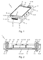
- FIG. 1 shows a three-dimensional view of a power semiconductor module 1 of an inventive arrangement 100 (see. Fig. 6 ), in which the cuboid basic shape of the power semiconductor module 1 is clearly visible.
- the power semiconductor module 1 thus has two main sides 2 a / b, on each of which closely adjacent to the longitudinal 3 a / b and narrow sides 4 a / b in opposite corners, the connection means 110, 120, 130, 140 are arranged for the cooling liquid. These connection devices 110, 120, 130, 140 are part of the cooling device 10 of the power semiconductor module 1.
- a flow outlet 120 and a return flow 140 are shown here.
- the cooling device 10 between the main surfaces 2 a / b penetrating recesses 18 are provided, which serve in the juxtaposition of a plurality of power semiconductor modules 1 to the connection.
- a housing 30 of the power semiconductor module 1 which covers the recess of the U-shaped cooling device 10 and thereby forms essential parts of the first main side 2a. Covered by the housing 30 and not visible, the power electronic circuit 22 of the power electronic switching device 20 of the power semiconductor module 1 is arranged. Load connection devices 24, 26, in this case load output connection devices 26, and control connection devices 28 are visible from the power electronic switching device 20. These penetrate the housing 30 at respectively assigned recesses 34, 36, 38, the load connection devices 24, 26 at longitudinal sections 3a / b, the control connection devices 28 on a narrow side 4a of the power semiconductor module 1.
- FIG. 2 schematically shows a plan view from the direction of a longitudinal side 3a on a section through a power semiconductor module 1 of an inventive arrangement 100.
- a U-shaped cooling device 10 which forms a second main side 2b and the two narrow sides 4 a / b of the power semiconductor module 1 approximately complete .
- the cooling device 10 forms a part of the first main side 2a, as well as parts of the two longitudinal sides 3 a / b (see. Fig. 1 ).
- the remaining parts of the first main side 2 a, as well as the remaining parts of the one narrow 4a and both longitudinal sides 3 a / b are formed by the housing 30.
- the cooling volume 16 of the cooling device 10 also has a second cooling surface 162, which at the same time forms part of the second main side 2b.
- This second cooling surface 162 serves as an example for the indirect cooling of a thermally connected thereto capacitor device, see. Fig. 6 ,
- the cooling liquid of the flow 12 passes in the power semiconductor module 1 through a flow inlet 110 at the second main side 2b in the cooling device 10 and is divided there by means of a first branch 122 into two partial streams.
- the essential part of the cooling liquid leaves the cooling device 10 of the power semiconductor module 1 through the flow outlet 120 on the first main side 2a, while a smaller proportion of the cooling liquid flows through the cooling volume 16 with adjacent cooling surface 160.
- the cooling liquid of the return 14 passes through this into the cooling device 10 and combines at a second branch 142 with the cooling liquid which has flowed through the cooling volume 16.
- the return 14 then exits the cooler 10 through the return drain 140 on the second main side 2b.
- this power semiconductor module 1 also has an internal control board 240, which is conventionally connected in circuit-compatible fashion with the switching modules 220 and with power semiconductor components arranged there and provides driver functionality for the power electronic circuit 22.
- This internal control board 240 has, as part of the electronic power switching device 20 on a narrow side 4a of the power semiconductor module 1 on a control terminal device 28 which projects through a recess 38 of the housing 30.
- FIG. 3 shows a plan view from the direction of a main page 2a on a power semiconductor module 1 according to the invention without a housing or indicated by dashed lines on an analog capacitor device formed 50th
- a cooling surface 160 on the three switching modules 220 of the power electronic circuit 22 are arranged.
- the load connection devices 24, 26 extending from these submodules 220 to the longitudinal sides 3 a / b are, like the auxiliary connection device 28 extending from these submodules 220 to a narrow side 4 a / b, not shown.
- the condenser device 50 with direct cooling is designed identically to the power semiconductor module with regard to the design of the cooling device. Instead of the switching modules of the power semiconductor module, three capacitors 58, shown in dashed lines, are provided in the capacitor device. Lastan gleich hearden the capacitor device are not shown, but may be provided on the first longitudinal side 3a.
- FIG. 4 shows in the upper part of a schematic plan view from the direction of a longitudinal side 3a on a section through a power semiconductor submodule 1b and in the lower part a corresponding plan view of an integrated capacitor device 50b of the inventive arrangement.
- the power semiconductor submodule 1b and the capacitor device 50b are connected directly to one another and thus form an integrated power semiconductor module 1a, that is, one with integrated capacitor device 50b.
- this integrated power semiconductor module 1a that is to say the power semiconductor submodule 1b and the integrated capacitor device 50b, is enclosed by a dustproof and moisture-proof encapsulation, which thus forms a common housing 30. Since the power semiconductor submodule 1b and the integrated capacitor device 50b are shown spaced apart from one another for reasons of clarity, the encapsulation 30 is shown at this distance in dashed lines.
- the power semiconductor submodule 1b in turn has a cooling device 10 analogous to that of the power semiconductor module according to FIG Fig. 2 on. However, here is the Flow inlet 110, as well as the return inflow 130 arranged on the second main side 2b. Accordingly, the advance drain 120 and the return drain 140 are disposed on the first main side 2a.
- the cooling volume 16 also forms not only a first cooling surface 160 for cooling the switching modules 220 of the power electronic switching device 20, but also a second of the first opposing cooling surface 162. This second cooling surface 162 is preferably in direct thermal contact with the capacitors 58 of the integrated Capacitor device 50b.
- This integrated capacitor device 50b like the power semiconductor submodule 1b, has a cuboidal basic shape. Furthermore, the integrated capacitor device 50b has its own cooling device 500 for direct cooling, which analogously to that of the power semiconductor submodule 1b has a flow inlet 510 and a return flow 530 on the second main side 502b.
- the two cooling devices 10, 500 of the power semiconductor submodule 1b and of the integrated capacitor device 50b are formed quasi in one piece.
- the respective cooling devices 10, 500 or the common cooling device formed therefrom must intrinsically also be formed in one piece.
- the cooling liquid of the flow 12 passes through a feed flow 110 on the second main side 502b into the cooling device 10, where it is split into two partial flows by means of a second branch 522.
- the essential part of the cooling liquid continues to flow to a first branch 122 where it is again divided and leaves the cooling device 10 of the integrated power semiconductor sub-module 1 b through the feed-out flow 120 the first main side 2a, while in each case a smaller proportion of the cooling liquid flows through the cooling volumes 16, 56 with adjacent cooling surfaces 160, 162, 560.
- Three capacitors 58 are arranged on the cooling surface 560 of the cooling device 500 of the integrated capacitor device 50b and are in thermal contact with the second cooling surface 162 of the power semiconductor submodule 1b and with the cooling surface 560 of the integrated capacitor device 50b. Thus, it is ensured that the capacitors 58 have excellent thermal contact with the cooling liquid. This is particularly necessary since the thermal load capacity of the capacitors 58 is often lower than that of the power semiconductor components of the switching modules 220.
- the power electronic switching device 20 of the power semiconductor submodule 1b is basically similar to that of the power semiconductor module according to FIG Fig. 2 formed and has switching modules 220, an internal control board 240 and control 28, load input 24 and Lastausgangsan gleich learneden 26. These control, load input and Lastausgangsan gleich respondeden serve the external connection of the power semiconductor submodule 1 b.
- an integrated power semiconductor module 1a ie as a power semiconductor submodule 1b with integrated capacitor device 50b
- the integrated capacitor device 50b has no external, ie externally connectable, load connection devices.
- the capacitors 58 of the integrated capacitor device 50b are internally connected to the associated load connection devices 24, 26 of the power semiconductor submodule 1b and externally connectable thereto.
- the capacitors 58 of the integrated capacitor device 50b are internally connected to the load input terminals 24 or the load output terminal devices 26 of the power semiconductor submodule 1b.
- the main sides of the integrated power semiconductor module 1a are formed from the first main side 2a of the power semiconductor submodule 1b and the second main side 502b of the integrated capacitor device 50b.
- the second main side 2 b of the power semiconductor submodule 1 b forms quasi only the second cooling surface 162 of the power semiconductor submodule 1 b, while the first main surface 502 a of the Capacitor device is formed essentially by the surface of the capacitors 58 to be cooled.
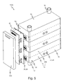
- FIG. 5 shows a three-dimensional view of a first embodiment of the inventive arrangement 100a. Shown here are three integrated power semiconductor modules 1 a, in turn, each consisting of a power semiconductor sub-module 1 b and a dashed, symbolic parting line, however, not actually separated therefrom capacitor device 50b, see. Fig. 4 ,
- the integrated power semiconductor modules 1a are directly connected to each other using suitable sealing devices. They thus lie directly against each other or have only a small distance from each other.
- the respective integrated power semiconductor modules 1a are connected to one another by means of a clamping device, not shown.
- the respective power semiconductor modules 1 a by means of screw, see. Fig. 2 to be connected.
- Each of the power semiconductor modules 1 a has load input terminal devices 24 on the same first longitudinal side 3 a visible here, which are here designed as DC voltage connection devices, which project through recesses 34 of the housing 30.
- the AC voltage terminal devices, the load output terminal devices, the inverter circuit realized with the power electronic switching devices of the power semiconductor modules 1a are arranged on the invisible second longitudinal sides.
- the auxiliary connection device 28 of all power semiconductor modules 1a of the arrangement 100a are arranged on a narrow side 4a of the respective power semiconductor modules 1a. This has the decisive advantage that the longitudinal sides 3 a / b are freely available for the formation of the external load connections. Thus, a particularly advantageous, for example, low-inductive external connection with this arrangement 100a can be realized.
- the auxiliary terminal devices 28 protrude through associated recesses 38 of the housing 30 and are here with a common external control board 40th connected, which may have different functionality. It can only serve the signal connection but also have complex control and monitoring functionality.
- the external control board 40 also has a sealing device 400 in order to be protected against environmental influences. This is particularly advantageous in combination with dust and moisture-proof encapsulated integrated power semiconductor modules 1a.
- FIG. 6 shows a three-dimensional view of a second embodiment of the inventive arrangement 100.
- a plurality of power semiconductor modules 1 are comparable to those according to Fig. 2 arranged alternately with capacitor devices 50.
- the power semiconductor modules 1 are connected directly or indirectly to each other by the flow outlet 120 of a power semiconductor module with the flow inlet 110 of the adjacent power semiconductor module and in the same way the return drain 140 of the power semiconductor module with the return flow 130 of the adjacent power semiconductor module is connected.
- connection can be formed directly or indirectly, ie with the interposition of connecting pieces.
- suitable sealing devices in both variants are provided in the usual way.
- the respective capacitor devices 50 do not have their own cooling devices and are thus exclusively indirectly cooled via cooling surfaces 162 of the power semiconductor modules 1.
- load connection devices 524 of the capacitor device 50 in the normal direction of the main surfaces 2 a / b are here shown in alignment with assigned load input connection devices 24 of the power semiconductor modules 1. This allows a particularly simple connection of external connection devices of the same polarity.
- the load output connection devices of the power semiconductor modules 1 are arranged on the second non-visible longitudinal sides. Auxiliary terminal devices are not shown here but of course providable on the narrow sides of the power semiconductor modules.
Landscapes
- Engineering & Computer Science (AREA)
- Microelectronics & Electronic Packaging (AREA)
- Physics & Mathematics (AREA)
- Power Engineering (AREA)
- Condensed Matter Physics & Semiconductors (AREA)
- General Physics & Mathematics (AREA)
- Computer Hardware Design (AREA)
- Thermal Sciences (AREA)
- Inverter Devices (AREA)
- Cooling Or The Like Of Semiconductors Or Solid State Devices (AREA)
- Cooling Or The Like Of Electrical Apparatus (AREA)
Applications Claiming Priority (1)
| Application Number | Priority Date | Filing Date | Title |
|---|---|---|---|
| DE102012206271A DE102012206271A1 (de) | 2012-04-17 | 2012-04-17 | Flüssigkeitsgekühlte Anordnung mit anreihbaren Leistungshalbleitermodulen und mindestens einer Kondensatoreinrichtung und Leistungshalbleitermodul hierzu |
Publications (3)
| Publication Number | Publication Date |
|---|---|
| EP2654391A2 true EP2654391A2 (fr) | 2013-10-23 |
| EP2654391A3 EP2654391A3 (fr) | 2017-02-15 |
| EP2654391B1 EP2654391B1 (fr) | 2018-11-28 |
Family
ID=47681758
Family Applications (1)
| Application Number | Title | Priority Date | Filing Date |
|---|---|---|---|
| EP13154128.6A Not-in-force EP2654391B1 (fr) | 2012-04-17 | 2013-02-06 | Agencement refroidi par liquide avec modules semi-conducteurs de puissance pouvant être joints et au moins un dispositif de condensateur et module semi-conducteur de puissance à cet effet |
Country Status (6)
| Country | Link |
|---|---|
| US (1) | US9165858B2 (fr) |
| EP (1) | EP2654391B1 (fr) |
| JP (1) | JP2013222974A (fr) |
| KR (1) | KR20130117671A (fr) |
| CN (2) | CN203386739U (fr) |
| DE (1) | DE102012206271A1 (fr) |
Families Citing this family (16)
| Publication number | Priority date | Publication date | Assignee | Title |
|---|---|---|---|---|
| DE102012206271A1 (de) * | 2012-04-17 | 2013-10-17 | Semikron Elektronik Gmbh & Co. Kg | Flüssigkeitsgekühlte Anordnung mit anreihbaren Leistungshalbleitermodulen und mindestens einer Kondensatoreinrichtung und Leistungshalbleitermodul hierzu |
| FR3002624B1 (fr) * | 2013-02-28 | 2015-02-27 | Bull Sas | Repartiteur hydraulique |
| JP6233257B2 (ja) * | 2014-04-15 | 2017-11-22 | トヨタ自動車株式会社 | 電力変換器 |
| US10264695B2 (en) * | 2014-09-25 | 2019-04-16 | Hitachi Automotive Systems, Ltd. | Power converter |
| CN106816803B (zh) * | 2015-11-27 | 2019-06-18 | 讯凯国际股份有限公司 | 泵浦模块及其泵浦 |
| CN108701688B (zh) | 2015-12-04 | 2021-11-09 | 罗姆股份有限公司 | 功率模块装置、冷却构造体、以及电动汽车或混合动力汽车 |
| CN109216291B (zh) * | 2017-06-29 | 2022-06-21 | 比亚迪半导体股份有限公司 | 用于功率模块的散热器和具有其的车辆 |
| DE102017212434A1 (de) * | 2017-07-20 | 2019-01-24 | Audi Ag | Elektronikeinrichtung mit wenigstens einer zu kühlenden Komponente |
| DE102018203362A1 (de) * | 2018-03-07 | 2019-09-12 | Robert Bosch Gmbh | Kühleinrichtung zur Kühlung eines Leistungsbauelements |
| JP7052447B2 (ja) * | 2018-03-16 | 2022-04-12 | 富士電機株式会社 | 電力変換装置 |
| JP7218828B2 (ja) * | 2018-03-16 | 2023-02-07 | 富士電機株式会社 | 電力変換装置 |
| CN110986651B (zh) * | 2019-12-10 | 2021-11-02 | 常州大学 | 一种翅片内具有换热腔体的翅片管换热器 |
| KR20210076689A (ko) | 2019-12-16 | 2021-06-24 | 삼성전자주식회사 | 열교환 모듈, 이를 포함하는 조립형 열교환기 및 열교환기 조립 시스템 |
| US10912231B1 (en) | 2020-01-15 | 2021-02-02 | Ford Global Technologies, Llc | Automotive integrated power module and capacitor |
| US11502349B2 (en) | 2020-08-31 | 2022-11-15 | Borgwarner, Inc. | Cooling manifold assembly |
| DE102022201329A1 (de) | 2022-02-09 | 2023-08-10 | Zf Friedrichshafen Ag | Schaltermodul für einen Inverter, Inverter mit mehreren solchen Schaltermodulen sowie Fahrzeug mit dem Inverter |
Citations (2)
| Publication number | Priority date | Publication date | Assignee | Title |
|---|---|---|---|---|
| DE10316356A1 (de) | 2003-04-10 | 2004-11-11 | Semikron Elektronik Gmbh | Modular aufgebautes Leistungshalbleitermodul |
| EP1815514B1 (fr) | 2004-11-24 | 2008-04-23 | Danfoss Silicon Power GmbH | Module de distribution de flux et pile de modules de distribution de flux |
Family Cites Families (21)
| Publication number | Priority date | Publication date | Assignee | Title |
|---|---|---|---|---|
| US5053856A (en) * | 1990-09-04 | 1991-10-01 | Sun Microsystems, Inc. | Apparatus for providing electrical conduits in compact arrays of electronic circuitry utilizing cooling devices |
| FR2765067B1 (fr) * | 1997-06-19 | 1999-07-16 | Alsthom Cge Alcatel | Module d'electronique de puissance et un dispositif d'electronique de puissance pourvu de tels modules |
| JP4423746B2 (ja) * | 2000-05-10 | 2010-03-03 | 株式会社デンソー | 冷媒冷却型両面冷却半導体装置 |
| JP4009056B2 (ja) * | 2000-05-25 | 2007-11-14 | 三菱電機株式会社 | パワーモジュール |
| EP2216890B1 (fr) * | 2003-08-21 | 2012-01-04 | Denso Corporation | Structure d'assemblage d'un dispositif à semi-conducteur |
| JP4225310B2 (ja) * | 2004-11-11 | 2009-02-18 | 株式会社デンソー | 半導体装置 |
| US8125781B2 (en) * | 2004-11-11 | 2012-02-28 | Denso Corporation | Semiconductor device |
| JP4661645B2 (ja) * | 2005-03-23 | 2011-03-30 | トヨタ自動車株式会社 | パワー半導体モジュール |
| CN101146429A (zh) * | 2006-09-15 | 2008-03-19 | 刘胜 | 电子器件的散热器 |
| JP4293246B2 (ja) * | 2007-02-19 | 2009-07-08 | 株式会社日立製作所 | 電力変換装置 |
| JP4683003B2 (ja) * | 2007-03-30 | 2011-05-11 | 株式会社デンソー | パワーモジュール及びこれを用いた電力変換装置 |
| JP2010135697A (ja) * | 2008-12-08 | 2010-06-17 | Toyota Motor Corp | 積層モジュール構造 |
| JP5212088B2 (ja) * | 2008-12-25 | 2013-06-19 | 株式会社デンソー | 半導体モジュール冷却装置 |
| JP5658435B2 (ja) | 2009-03-31 | 2015-01-28 | リンテック株式会社 | マスクフィルム用部材、それを用いたマスクフィルムの製造方法及び感光性樹脂印刷版の製造方法 |
| JP4775475B2 (ja) * | 2009-04-14 | 2011-09-21 | 株式会社デンソー | 電力変換装置 |
| US7952875B2 (en) * | 2009-05-29 | 2011-05-31 | GM Global Technology Operations LLC | Stacked busbar assembly with integrated cooling |
| JP5327195B2 (ja) * | 2010-02-05 | 2013-10-30 | 株式会社デンソー | 電力変換装置 |
| JP5115632B2 (ja) * | 2010-06-30 | 2013-01-09 | 株式会社デンソー | 半導体装置 |
| JP5392196B2 (ja) * | 2010-06-30 | 2014-01-22 | 株式会社デンソー | 半導体装置 |
| RU2014125069A (ru) * | 2011-12-20 | 2016-02-10 | Тойота Дзидося Кабусики Кайся | Полупроводниковый модуль |
| DE102012206271A1 (de) * | 2012-04-17 | 2013-10-17 | Semikron Elektronik Gmbh & Co. Kg | Flüssigkeitsgekühlte Anordnung mit anreihbaren Leistungshalbleitermodulen und mindestens einer Kondensatoreinrichtung und Leistungshalbleitermodul hierzu |
-
2012
- 2012-04-17 DE DE102012206271A patent/DE102012206271A1/de not_active Withdrawn
-
2013
- 2013-02-06 EP EP13154128.6A patent/EP2654391B1/fr not_active Not-in-force
- 2013-04-05 KR KR1020130037368A patent/KR20130117671A/ko not_active Application Discontinuation
- 2013-04-16 CN CN201320191489.6U patent/CN203386739U/zh not_active Withdrawn - After Issue
- 2013-04-16 JP JP2013085613A patent/JP2013222974A/ja active Pending
- 2013-04-16 CN CN201310130929.1A patent/CN103378027B/zh not_active Expired - Fee Related
- 2013-04-17 US US13/865,184 patent/US9165858B2/en not_active Expired - Fee Related
Patent Citations (2)
| Publication number | Priority date | Publication date | Assignee | Title |
|---|---|---|---|---|
| DE10316356A1 (de) | 2003-04-10 | 2004-11-11 | Semikron Elektronik Gmbh | Modular aufgebautes Leistungshalbleitermodul |
| EP1815514B1 (fr) | 2004-11-24 | 2008-04-23 | Danfoss Silicon Power GmbH | Module de distribution de flux et pile de modules de distribution de flux |
Also Published As
| Publication number | Publication date |
|---|---|
| CN103378027B (zh) | 2018-11-02 |
| US9165858B2 (en) | 2015-10-20 |
| CN103378027A (zh) | 2013-10-30 |
| JP2013222974A (ja) | 2013-10-28 |
| EP2654391A3 (fr) | 2017-02-15 |
| US20130271917A1 (en) | 2013-10-17 |
| DE102012206271A1 (de) | 2013-10-17 |
| CN203386739U (zh) | 2014-01-08 |
| KR20130117671A (ko) | 2013-10-28 |
| EP2654391B1 (fr) | 2018-11-28 |
Similar Documents
| Publication | Publication Date | Title |
|---|---|---|
| EP2654391B1 (fr) | Agencement refroidi par liquide avec modules semi-conducteurs de puissance pouvant être joints et au moins un dispositif de condensateur et module semi-conducteur de puissance à cet effet | |
| EP2654392B1 (fr) | Module semi-conducteur de puissance refroidi par liquide pouvant être joint et agencement à cet effet | |
| EP2272311B1 (fr) | Dispositif de refroidissement pour une pluralité de modules de puissance | |
| EP2364581B1 (fr) | Module redresseur de courant à système de barres refroidi | |
| EP1848260B1 (fr) | Onduleur | |
| DE102014213084B4 (de) | Halbleitervorrichtung | |
| EP2458633A2 (fr) | Système semi-conducteur de puissance | |
| DE102005034998B4 (de) | Verfahren zur Herstellung einer Vorrichtung zur Kühlung von elektronischen Bauelementen sowie Vorrichtung zur Kühlung von elektronischen Bauelementen | |
| DE202012012767U1 (de) | Leistungshalbleitermodulsystem | |
| WO2012152551A1 (fr) | Système électronique de puissance muni d'un dispositif de refroidissement par liquide | |
| EP2528091A2 (fr) | Système électronique de puissance avec sous-systèmes et dispositif de refroidissement | |
| DE102016103788A1 (de) | Kunststoffkühler für Halbleitermodule | |
| DE112018000105T5 (de) | Elektronisches bauelement und leistungsumwandlungseinrichtung | |
| EP2521432A2 (fr) | Agencement de puissance électronique doté d'un refroidissement de liquide | |
| DE102012215787B4 (de) | Leistungselektronisches System mit Flüssigkeitskühleinrichtung und Fahrzeug damit | |
| EP3328678A1 (fr) | Batterie de traction pour véhicule à moteur munie d'un dispositif de refroidissement | |
| DE102017005315A1 (de) | Batteriekasten | |
| DE102005031759A1 (de) | Stromrichteranordnung mit Kühleinrichtung | |
| DE102008058032A1 (de) | Mikrostrukturkühler für ein elektrisches oder elektronisches Bauteil | |
| EP3762964A1 (fr) | Dispositif de refroidissement pour refroidir un composant de puissance | |
| EP1739804A1 (fr) | Rail de support conducteur de courant d'un ou de plusieurs appareils électriques | |
| EP1758165B1 (fr) | Module semi-conducteur de puissance à moyens de fixation contre un dissipateur | |
| DE102018209548A1 (de) | Kondensatorträgermaterialeinheit zum Öffnen/Schließen eines Moduls | |
| DE102011100524B4 (de) | Leistungselektronische Anordnung | |
| DE102017214487A1 (de) | Stapelbares Kühlkörpermodul |
Legal Events
| Date | Code | Title | Description |
|---|---|---|---|
| PUAI | Public reference made under article 153(3) epc to a published international application that has entered the european phase |
Free format text: ORIGINAL CODE: 0009012 |
|
| AK | Designated contracting states |
Kind code of ref document: A2 Designated state(s): AL AT BE BG CH CY CZ DE DK EE ES FI FR GB GR HR HU IE IS IT LI LT LU LV MC MK MT NL NO PL PT RO RS SE SI SK SM TR |
|
| AX | Request for extension of the european patent |
Extension state: BA ME |
|
| PUAL | Search report despatched |
Free format text: ORIGINAL CODE: 0009013 |
|
| AK | Designated contracting states |
Kind code of ref document: A3 Designated state(s): AL AT BE BG CH CY CZ DE DK EE ES FI FR GB GR HR HU IE IS IT LI LT LU LV MC MK MT NL NO PL PT RO RS SE SI SK SM TR |
|
| AX | Request for extension of the european patent |
Extension state: BA ME |
|
| RIC1 | Information provided on ipc code assigned before grant |
Ipc: H01L 23/473 20060101ALI20170112BHEP Ipc: H05K 7/20 20060101AFI20170112BHEP Ipc: H01L 25/07 20060101ALI20170112BHEP Ipc: H01L 25/11 20060101ALI20170112BHEP |
|
| STAA | Information on the status of an ep patent application or granted ep patent |
Free format text: STATUS: REQUEST FOR EXAMINATION WAS MADE |
|
| 17P | Request for examination filed |
Effective date: 20170816 |
|
| RBV | Designated contracting states (corrected) |
Designated state(s): AL AT BE BG CH CY CZ DE DK EE ES FI FR GB GR HR HU IE IS IT LI LT LU LV MC MK MT NL NO PL PT RO RS SE SI SK SM TR |
|
| GRAP | Despatch of communication of intention to grant a patent |
Free format text: ORIGINAL CODE: EPIDOSNIGR1 |
|
| STAA | Information on the status of an ep patent application or granted ep patent |
Free format text: STATUS: GRANT OF PATENT IS INTENDED |
|
| INTG | Intention to grant announced |
Effective date: 20180903 |
|
| GRAS | Grant fee paid |
Free format text: ORIGINAL CODE: EPIDOSNIGR3 |
|
| GRAA | (expected) grant |
Free format text: ORIGINAL CODE: 0009210 |
|
| STAA | Information on the status of an ep patent application or granted ep patent |
Free format text: STATUS: THE PATENT HAS BEEN GRANTED |
|
| AK | Designated contracting states |
Kind code of ref document: B1 Designated state(s): AL AT BE BG CH CY CZ DE DK EE ES FI FR GB GR HR HU IE IS IT LI LT LU LV MC MK MT NL NO PL PT RO RS SE SI SK SM TR |
|
| REG | Reference to a national code |
Ref country code: GB Ref legal event code: FG4D Free format text: NOT ENGLISH |
|
| REG | Reference to a national code |
Ref country code: CH Ref legal event code: EP |
|
| REG | Reference to a national code |
Ref country code: AT Ref legal event code: REF Ref document number: 1071846 Country of ref document: AT Kind code of ref document: T Effective date: 20181215 |
|
| REG | Reference to a national code |
Ref country code: DE Ref legal event code: R096 Ref document number: 502013011689 Country of ref document: DE |
|
| REG | Reference to a national code |
Ref country code: IE Ref legal event code: FG4D Free format text: LANGUAGE OF EP DOCUMENT: GERMAN |
|
| REG | Reference to a national code |
Ref country code: NL Ref legal event code: MP Effective date: 20181128 |
|
| REG | Reference to a national code |
Ref country code: LT Ref legal event code: MG4D |
|
| PG25 | Lapsed in a contracting state [announced via postgrant information from national office to epo] |
Ref country code: IS Free format text: LAPSE BECAUSE OF FAILURE TO SUBMIT A TRANSLATION OF THE DESCRIPTION OR TO PAY THE FEE WITHIN THE PRESCRIBED TIME-LIMIT Effective date: 20190328 Ref country code: FI Free format text: LAPSE BECAUSE OF FAILURE TO SUBMIT A TRANSLATION OF THE DESCRIPTION OR TO PAY THE FEE WITHIN THE PRESCRIBED TIME-LIMIT Effective date: 20181128 Ref country code: LV Free format text: LAPSE BECAUSE OF FAILURE TO SUBMIT A TRANSLATION OF THE DESCRIPTION OR TO PAY THE FEE WITHIN THE PRESCRIBED TIME-LIMIT Effective date: 20181128 Ref country code: HR Free format text: LAPSE BECAUSE OF FAILURE TO SUBMIT A TRANSLATION OF THE DESCRIPTION OR TO PAY THE FEE WITHIN THE PRESCRIBED TIME-LIMIT Effective date: 20181128 Ref country code: NO Free format text: LAPSE BECAUSE OF FAILURE TO SUBMIT A TRANSLATION OF THE DESCRIPTION OR TO PAY THE FEE WITHIN THE PRESCRIBED TIME-LIMIT Effective date: 20190228 Ref country code: BG Free format text: LAPSE BECAUSE OF FAILURE TO SUBMIT A TRANSLATION OF THE DESCRIPTION OR TO PAY THE FEE WITHIN THE PRESCRIBED TIME-LIMIT Effective date: 20190228 Ref country code: ES Free format text: LAPSE BECAUSE OF FAILURE TO SUBMIT A TRANSLATION OF THE DESCRIPTION OR TO PAY THE FEE WITHIN THE PRESCRIBED TIME-LIMIT Effective date: 20181128 Ref country code: LT Free format text: LAPSE BECAUSE OF FAILURE TO SUBMIT A TRANSLATION OF THE DESCRIPTION OR TO PAY THE FEE WITHIN THE PRESCRIBED TIME-LIMIT Effective date: 20181128 |
|
| PG25 | Lapsed in a contracting state [announced via postgrant information from national office to epo] |
Ref country code: PT Free format text: LAPSE BECAUSE OF FAILURE TO SUBMIT A TRANSLATION OF THE DESCRIPTION OR TO PAY THE FEE WITHIN THE PRESCRIBED TIME-LIMIT Effective date: 20190328 Ref country code: RS Free format text: LAPSE BECAUSE OF FAILURE TO SUBMIT A TRANSLATION OF THE DESCRIPTION OR TO PAY THE FEE WITHIN THE PRESCRIBED TIME-LIMIT Effective date: 20181128 Ref country code: SE Free format text: LAPSE BECAUSE OF FAILURE TO SUBMIT A TRANSLATION OF THE DESCRIPTION OR TO PAY THE FEE WITHIN THE PRESCRIBED TIME-LIMIT Effective date: 20181128 Ref country code: GR Free format text: LAPSE BECAUSE OF FAILURE TO SUBMIT A TRANSLATION OF THE DESCRIPTION OR TO PAY THE FEE WITHIN THE PRESCRIBED TIME-LIMIT Effective date: 20190301 Ref country code: AL Free format text: LAPSE BECAUSE OF FAILURE TO SUBMIT A TRANSLATION OF THE DESCRIPTION OR TO PAY THE FEE WITHIN THE PRESCRIBED TIME-LIMIT Effective date: 20181128 |
|
| PG25 | Lapsed in a contracting state [announced via postgrant information from national office to epo] |
Ref country code: NL Free format text: LAPSE BECAUSE OF FAILURE TO SUBMIT A TRANSLATION OF THE DESCRIPTION OR TO PAY THE FEE WITHIN THE PRESCRIBED TIME-LIMIT Effective date: 20181128 |
|
| PG25 | Lapsed in a contracting state [announced via postgrant information from national office to epo] |
Ref country code: IT Free format text: LAPSE BECAUSE OF FAILURE TO SUBMIT A TRANSLATION OF THE DESCRIPTION OR TO PAY THE FEE WITHIN THE PRESCRIBED TIME-LIMIT Effective date: 20181128 Ref country code: CZ Free format text: LAPSE BECAUSE OF FAILURE TO SUBMIT A TRANSLATION OF THE DESCRIPTION OR TO PAY THE FEE WITHIN THE PRESCRIBED TIME-LIMIT Effective date: 20181128 Ref country code: DK Free format text: LAPSE BECAUSE OF FAILURE TO SUBMIT A TRANSLATION OF THE DESCRIPTION OR TO PAY THE FEE WITHIN THE PRESCRIBED TIME-LIMIT Effective date: 20181128 Ref country code: PL Free format text: LAPSE BECAUSE OF FAILURE TO SUBMIT A TRANSLATION OF THE DESCRIPTION OR TO PAY THE FEE WITHIN THE PRESCRIBED TIME-LIMIT Effective date: 20181128 |
|
| REG | Reference to a national code |
Ref country code: DE Ref legal event code: R097 Ref document number: 502013011689 Country of ref document: DE |
|
| PG25 | Lapsed in a contracting state [announced via postgrant information from national office to epo] |
Ref country code: EE Free format text: LAPSE BECAUSE OF FAILURE TO SUBMIT A TRANSLATION OF THE DESCRIPTION OR TO PAY THE FEE WITHIN THE PRESCRIBED TIME-LIMIT Effective date: 20181128 Ref country code: SM Free format text: LAPSE BECAUSE OF FAILURE TO SUBMIT A TRANSLATION OF THE DESCRIPTION OR TO PAY THE FEE WITHIN THE PRESCRIBED TIME-LIMIT Effective date: 20181128 Ref country code: RO Free format text: LAPSE BECAUSE OF FAILURE TO SUBMIT A TRANSLATION OF THE DESCRIPTION OR TO PAY THE FEE WITHIN THE PRESCRIBED TIME-LIMIT Effective date: 20181128 Ref country code: SK Free format text: LAPSE BECAUSE OF FAILURE TO SUBMIT A TRANSLATION OF THE DESCRIPTION OR TO PAY THE FEE WITHIN THE PRESCRIBED TIME-LIMIT Effective date: 20181128 |
|
| REG | Reference to a national code |
Ref country code: CH Ref legal event code: PL |
|
| PLBE | No opposition filed within time limit |
Free format text: ORIGINAL CODE: 0009261 |
|
| STAA | Information on the status of an ep patent application or granted ep patent |
Free format text: STATUS: NO OPPOSITION FILED WITHIN TIME LIMIT |
|
| GBPC | Gb: european patent ceased through non-payment of renewal fee |
Effective date: 20190228 |
|
| PG25 | Lapsed in a contracting state [announced via postgrant information from national office to epo] |
Ref country code: LU Free format text: LAPSE BECAUSE OF NON-PAYMENT OF DUE FEES Effective date: 20190206 Ref country code: MC Free format text: LAPSE BECAUSE OF FAILURE TO SUBMIT A TRANSLATION OF THE DESCRIPTION OR TO PAY THE FEE WITHIN THE PRESCRIBED TIME-LIMIT Effective date: 20181128 Ref country code: SI Free format text: LAPSE BECAUSE OF FAILURE TO SUBMIT A TRANSLATION OF THE DESCRIPTION OR TO PAY THE FEE WITHIN THE PRESCRIBED TIME-LIMIT Effective date: 20181128 |
|
| 26N | No opposition filed |
Effective date: 20190829 |
|
| REG | Reference to a national code |
Ref country code: BE Ref legal event code: MM Effective date: 20190228 |
|
| REG | Reference to a national code |
Ref country code: IE Ref legal event code: MM4A |
|
| PG25 | Lapsed in a contracting state [announced via postgrant information from national office to epo] |
Ref country code: CH Free format text: LAPSE BECAUSE OF NON-PAYMENT OF DUE FEES Effective date: 20190228 Ref country code: LI Free format text: LAPSE BECAUSE OF NON-PAYMENT OF DUE FEES Effective date: 20190228 |
|
| PG25 | Lapsed in a contracting state [announced via postgrant information from national office to epo] |
Ref country code: GB Free format text: LAPSE BECAUSE OF NON-PAYMENT OF DUE FEES Effective date: 20190228 Ref country code: IE Free format text: LAPSE BECAUSE OF NON-PAYMENT OF DUE FEES Effective date: 20190206 |
|
| PG25 | Lapsed in a contracting state [announced via postgrant information from national office to epo] |
Ref country code: BE Free format text: LAPSE BECAUSE OF NON-PAYMENT OF DUE FEES Effective date: 20190228 Ref country code: FR Free format text: LAPSE BECAUSE OF NON-PAYMENT OF DUE FEES Effective date: 20190228 |
|
| PG25 | Lapsed in a contracting state [announced via postgrant information from national office to epo] |
Ref country code: TR Free format text: LAPSE BECAUSE OF FAILURE TO SUBMIT A TRANSLATION OF THE DESCRIPTION OR TO PAY THE FEE WITHIN THE PRESCRIBED TIME-LIMIT Effective date: 20181128 |
|
| REG | Reference to a national code |
Ref country code: AT Ref legal event code: MM01 Ref document number: 1071846 Country of ref document: AT Kind code of ref document: T Effective date: 20190206 |
|
| PG25 | Lapsed in a contracting state [announced via postgrant information from national office to epo] |
Ref country code: AT Free format text: LAPSE BECAUSE OF NON-PAYMENT OF DUE FEES Effective date: 20190206 |
|
| PGFP | Annual fee paid to national office [announced via postgrant information from national office to epo] |
Ref country code: DE Payment date: 20200229 Year of fee payment: 8 |
|
| PG25 | Lapsed in a contracting state [announced via postgrant information from national office to epo] |
Ref country code: MT Free format text: LAPSE BECAUSE OF FAILURE TO SUBMIT A TRANSLATION OF THE DESCRIPTION OR TO PAY THE FEE WITHIN THE PRESCRIBED TIME-LIMIT Effective date: 20181128 |
|
| PG25 | Lapsed in a contracting state [announced via postgrant information from national office to epo] |
Ref country code: CY Free format text: LAPSE BECAUSE OF FAILURE TO SUBMIT A TRANSLATION OF THE DESCRIPTION OR TO PAY THE FEE WITHIN THE PRESCRIBED TIME-LIMIT Effective date: 20181128 |
|
| PG25 | Lapsed in a contracting state [announced via postgrant information from national office to epo] |
Ref country code: HU Free format text: LAPSE BECAUSE OF FAILURE TO SUBMIT A TRANSLATION OF THE DESCRIPTION OR TO PAY THE FEE WITHIN THE PRESCRIBED TIME-LIMIT; INVALID AB INITIO Effective date: 20130206 |
|
| REG | Reference to a national code |
Ref country code: DE Ref legal event code: R119 Ref document number: 502013011689 Country of ref document: DE |
|
| PG25 | Lapsed in a contracting state [announced via postgrant information from national office to epo] |
Ref country code: DE Free format text: LAPSE BECAUSE OF NON-PAYMENT OF DUE FEES Effective date: 20210901 |
|
| PG25 | Lapsed in a contracting state [announced via postgrant information from national office to epo] |
Ref country code: MK Free format text: LAPSE BECAUSE OF FAILURE TO SUBMIT A TRANSLATION OF THE DESCRIPTION OR TO PAY THE FEE WITHIN THE PRESCRIBED TIME-LIMIT Effective date: 20181128 |