EP2654391A2 - Liquid-cooled assembly with in-line power semiconductor modules and at least one capacitor device and power semiconductor module therefor - Google Patents
Liquid-cooled assembly with in-line power semiconductor modules and at least one capacitor device and power semiconductor module therefor Download PDFInfo
- Publication number
- EP2654391A2 EP2654391A2 EP13154128.6A EP13154128A EP2654391A2 EP 2654391 A2 EP2654391 A2 EP 2654391A2 EP 13154128 A EP13154128 A EP 13154128A EP 2654391 A2 EP2654391 A2 EP 2654391A2
- Authority
- EP
- European Patent Office
- Prior art keywords
- power semiconductor
- cooling
- flow
- semiconductor module
- integrated
- Prior art date
- Legal status (The legal status is an assumption and is not a legal conclusion. Google has not performed a legal analysis and makes no representation as to the accuracy of the status listed.)
- Granted
Links
- 239000004065 semiconductor Substances 0.000 title claims abstract description 147
- 239000003990 capacitor Substances 0.000 title claims abstract description 69
- 238000001816 cooling Methods 0.000 claims abstract description 99
- 239000000110 cooling liquid Substances 0.000 claims description 25
- 239000000428 dust Substances 0.000 claims description 3
- 239000012809 cooling fluid Substances 0.000 claims description 2
- 239000002826 coolant Substances 0.000 claims 1
- 238000007789 sealing Methods 0.000 description 5
- 239000007788 liquid Substances 0.000 description 4
- 238000005538 encapsulation Methods 0.000 description 2
- 230000015572 biosynthetic process Effects 0.000 description 1
- 230000001419 dependent effect Effects 0.000 description 1
- 230000007613 environmental effect Effects 0.000 description 1
- 238000009499 grossing Methods 0.000 description 1
- 238000007373 indentation Methods 0.000 description 1
- 238000012544 monitoring process Methods 0.000 description 1
- 230000000149 penetrating effect Effects 0.000 description 1
- 239000000565 sealant Substances 0.000 description 1
- 230000009469 supplementation Effects 0.000 description 1
- 230000032258 transport Effects 0.000 description 1
Images


Classifications
-
- H—ELECTRICITY
- H01—ELECTRIC ELEMENTS
- H01L—SEMICONDUCTOR DEVICES NOT COVERED BY CLASS H10
- H01L23/00—Details of semiconductor or other solid state devices
- H01L23/34—Arrangements for cooling, heating, ventilating or temperature compensation ; Temperature sensing arrangements
- H01L23/46—Arrangements for cooling, heating, ventilating or temperature compensation ; Temperature sensing arrangements involving the transfer of heat by flowing fluids
- H01L23/473—Arrangements for cooling, heating, ventilating or temperature compensation ; Temperature sensing arrangements involving the transfer of heat by flowing fluids by flowing liquids
-
- H—ELECTRICITY
- H01—ELECTRIC ELEMENTS
- H01H—ELECTRIC SWITCHES; RELAYS; SELECTORS; EMERGENCY PROTECTIVE DEVICES
- H01H9/00—Details of switching devices, not covered by groups H01H1/00 - H01H7/00
- H01H9/52—Cooling of switch parts
-
- H—ELECTRICITY
- H01—ELECTRIC ELEMENTS
- H01L—SEMICONDUCTOR DEVICES NOT COVERED BY CLASS H10
- H01L23/00—Details of semiconductor or other solid state devices
- H01L23/02—Containers; Seals
- H01L23/06—Containers; Seals characterised by the material of the container or its electrical properties
-
- H—ELECTRICITY
- H01—ELECTRIC ELEMENTS
- H01L—SEMICONDUCTOR DEVICES NOT COVERED BY CLASS H10
- H01L23/00—Details of semiconductor or other solid state devices
- H01L23/34—Arrangements for cooling, heating, ventilating or temperature compensation ; Temperature sensing arrangements
- H01L23/40—Mountings or securing means for detachable cooling or heating arrangements ; fixed by friction, plugs or springs
- H01L23/4006—Mountings or securing means for detachable cooling or heating arrangements ; fixed by friction, plugs or springs with bolts or screws
- H01L23/4012—Mountings or securing means for detachable cooling or heating arrangements ; fixed by friction, plugs or springs with bolts or screws for stacked arrangements of a plurality of semiconductor devices
-
- H—ELECTRICITY
- H01—ELECTRIC ELEMENTS
- H01L—SEMICONDUCTOR DEVICES NOT COVERED BY CLASS H10
- H01L25/00—Assemblies consisting of a plurality of individual semiconductor or other solid state devices ; Multistep manufacturing processes thereof
- H01L25/03—Assemblies consisting of a plurality of individual semiconductor or other solid state devices ; Multistep manufacturing processes thereof all the devices being of a type provided for in the same subgroup of groups H01L27/00 - H01L33/00, or in a single subclass of H10K, H10N, e.g. assemblies of rectifier diodes
- H01L25/04—Assemblies consisting of a plurality of individual semiconductor or other solid state devices ; Multistep manufacturing processes thereof all the devices being of a type provided for in the same subgroup of groups H01L27/00 - H01L33/00, or in a single subclass of H10K, H10N, e.g. assemblies of rectifier diodes the devices not having separate containers
- H01L25/065—Assemblies consisting of a plurality of individual semiconductor or other solid state devices ; Multistep manufacturing processes thereof all the devices being of a type provided for in the same subgroup of groups H01L27/00 - H01L33/00, or in a single subclass of H10K, H10N, e.g. assemblies of rectifier diodes the devices not having separate containers the devices being of a type provided for in group H01L27/00
-
- H—ELECTRICITY
- H01—ELECTRIC ELEMENTS
- H01L—SEMICONDUCTOR DEVICES NOT COVERED BY CLASS H10
- H01L25/00—Assemblies consisting of a plurality of individual semiconductor or other solid state devices ; Multistep manufacturing processes thereof
- H01L25/03—Assemblies consisting of a plurality of individual semiconductor or other solid state devices ; Multistep manufacturing processes thereof all the devices being of a type provided for in the same subgroup of groups H01L27/00 - H01L33/00, or in a single subclass of H10K, H10N, e.g. assemblies of rectifier diodes
- H01L25/10—Assemblies consisting of a plurality of individual semiconductor or other solid state devices ; Multistep manufacturing processes thereof all the devices being of a type provided for in the same subgroup of groups H01L27/00 - H01L33/00, or in a single subclass of H10K, H10N, e.g. assemblies of rectifier diodes the devices having separate containers
- H01L25/11—Assemblies consisting of a plurality of individual semiconductor or other solid state devices ; Multistep manufacturing processes thereof all the devices being of a type provided for in the same subgroup of groups H01L27/00 - H01L33/00, or in a single subclass of H10K, H10N, e.g. assemblies of rectifier diodes the devices having separate containers the devices being of a type provided for in group H01L29/00
- H01L25/117—Stacked arrangements of devices
-
- H—ELECTRICITY
- H05—ELECTRIC TECHNIQUES NOT OTHERWISE PROVIDED FOR
- H05K—PRINTED CIRCUITS; CASINGS OR CONSTRUCTIONAL DETAILS OF ELECTRIC APPARATUS; MANUFACTURE OF ASSEMBLAGES OF ELECTRICAL COMPONENTS
- H05K7/00—Constructional details common to different types of electric apparatus
- H05K7/20—Modifications to facilitate cooling, ventilating, or heating
- H05K7/2089—Modifications to facilitate cooling, ventilating, or heating for power electronics, e.g. for inverters for controlling motor
- H05K7/20927—Liquid coolant without phase change
-
- H—ELECTRICITY
- H01—ELECTRIC ELEMENTS
- H01L—SEMICONDUCTOR DEVICES NOT COVERED BY CLASS H10
- H01L23/00—Details of semiconductor or other solid state devices
- H01L23/34—Arrangements for cooling, heating, ventilating or temperature compensation ; Temperature sensing arrangements
-
- H—ELECTRICITY
- H01—ELECTRIC ELEMENTS
- H01L—SEMICONDUCTOR DEVICES NOT COVERED BY CLASS H10
- H01L23/00—Details of semiconductor or other solid state devices
- H01L23/34—Arrangements for cooling, heating, ventilating or temperature compensation ; Temperature sensing arrangements
- H01L23/36—Selection of materials, or shaping, to facilitate cooling or heating, e.g. heatsinks
-
- H—ELECTRICITY
- H01—ELECTRIC ELEMENTS
- H01L—SEMICONDUCTOR DEVICES NOT COVERED BY CLASS H10
- H01L25/00—Assemblies consisting of a plurality of individual semiconductor or other solid state devices ; Multistep manufacturing processes thereof
- H01L25/03—Assemblies consisting of a plurality of individual semiconductor or other solid state devices ; Multistep manufacturing processes thereof all the devices being of a type provided for in the same subgroup of groups H01L27/00 - H01L33/00, or in a single subclass of H10K, H10N, e.g. assemblies of rectifier diodes
- H01L25/04—Assemblies consisting of a plurality of individual semiconductor or other solid state devices ; Multistep manufacturing processes thereof all the devices being of a type provided for in the same subgroup of groups H01L27/00 - H01L33/00, or in a single subclass of H10K, H10N, e.g. assemblies of rectifier diodes the devices not having separate containers
- H01L25/07—Assemblies consisting of a plurality of individual semiconductor or other solid state devices ; Multistep manufacturing processes thereof all the devices being of a type provided for in the same subgroup of groups H01L27/00 - H01L33/00, or in a single subclass of H10K, H10N, e.g. assemblies of rectifier diodes the devices not having separate containers the devices being of a type provided for in group H01L29/00
- H01L25/074—Stacked arrangements of non-apertured devices
-
- H—ELECTRICITY
- H01—ELECTRIC ELEMENTS
- H01L—SEMICONDUCTOR DEVICES NOT COVERED BY CLASS H10
- H01L2924/00—Indexing scheme for arrangements or methods for connecting or disconnecting semiconductor or solid-state bodies as covered by H01L24/00
- H01L2924/0001—Technical content checked by a classifier
- H01L2924/0002—Not covered by any one of groups H01L24/00, H01L24/00 and H01L2224/00
Landscapes
- Engineering & Computer Science (AREA)
- Microelectronics & Electronic Packaging (AREA)
- Physics & Mathematics (AREA)
- Power Engineering (AREA)
- Condensed Matter Physics & Semiconductors (AREA)
- General Physics & Mathematics (AREA)
- Computer Hardware Design (AREA)
- Thermal Sciences (AREA)
- Inverter Devices (AREA)
- Cooling Or The Like Of Semiconductors Or Solid State Devices (AREA)
- Cooling Or The Like Of Electrical Apparatus (AREA)
Abstract
Description
Die Erfindung beschreibt eine Anordnung mit anreihbaren Leistungshalbleitermodulen und mindestens einer Kondensatoreinrichtung insbesondere geeignet für den Einsatz in dezentralen Energieversorgungseinrichtungen. Hierfür ist die Anordnung mit einer Flüssigkeitskühleinrichtung vorgesehen und derart ausgebildet, dass sie beispielhaft als Wechselrichterschaltung in Windkraftanlagen einsetzbar ist.The invention describes an arrangement with arrangable power semiconductor modules and at least one capacitor device, in particular suitable for use in decentralized power supply devices. For this purpose, the arrangement is provided with a liquid cooling device and designed such that it can be used by way of example as an inverter circuit in wind turbines.
Grundsätzlich sind anreihbare Leistungshalbleitermodule und Anordnungen hieraus beispielhaft aus der
Weiterhin sind aus der
In Kenntnis dieses Standes der Technik liegt der Erfindung die Aufgabe zugrunde, derartige Anordnungen weiterzubilden, dass sie in Kombination mit einer Flüssigkeitskühlung besonders kompakt aufgebaut sind und gleichzeitig einer flexiblen und besonders geeigneten externen Verbindung zugänglich ist. Ebenso ist es Aufgabe der Erfindung ein besonders vorteilhaftes Leistungshalbleitermodul für eine derartige Anordnung vorzustellen.In view of this prior art, the invention has the object of developing such arrangements that they are particularly compact in combination with a liquid cooling and at the same time a flexible and particularly suitable external connection is accessible. It is likewise an object of the invention to present a particularly advantageous power semiconductor module for such an arrangement.
Diese Aufgabe wird erfindungsgemäß gelöst durch eine Anordnung mit den Merkmalen des Anspruchs 1 oder 14 und einem Leistungshalbleitermodul gemäß Anspruch 11 hierzu. Bevorzugte Ausführungsformen sind in den jeweiligen abhängigen Ansprüchen beschrieben.This object is achieved by an arrangement with the features of
Die erfindungsgemäße Anordnung weist einen Kühlkreislauf, einer Mehrzahl von anreihbaren Leistungshalbleitermodulen und mindestens eine Kondensatoreinrichtung auf. Hierbei weist das jeweilige Leistungshalbleitermodul eine quaderförmige Grundform auf, wodurch zwei Haupt-, zwei Längs- und zwei Schmalseiten, die sich jeweils paarweise gegenüberliegen, definiert werden. Die Hauptseiten sind weiterhin dadurch definiert, dass bezogen auf die quaderförmige Grundform ihr Flächeninhalt der größte ist, während entsprechend derjenige Flächeninhalt der Schmalseiten der kleinste ist. Diese jeweiligen Seiten bilden unter Beibehaltung der quaderförmigen Grundform nicht zwangsläufig vollständig ebenen Flächen aus, vielmehr können die Flächen der jeweiligen Seiten Einzüge und alternativ oder zusätzlich Ausnehmungen, beispielhaft für Anschlusselemente aufweisen.The arrangement according to the invention has a cooling circuit, a plurality of arrangable power semiconductor modules and at least one capacitor device. In this case, the respective power semiconductor module has a cuboid basic shape, whereby two main, two longitudinal and two narrow sides, which are opposite each other in pairs, are defined. The main pages are further defined by the fact that based on the cuboid basic shape their area is the largest, while correspondingly that area of the narrow sides is the smallest. While retaining the cuboid basic shape, these respective sides do not necessarily form completely flat surfaces; rather, the surfaces of the respective sides can have indentations and, alternatively or additionally, recesses, for example for connecting elements.
Weiterhin weist jedes Leistungshalbleitermodul eine leistungselektronische Schalteinrichtung und eine durchströmbare Kühleinrichtung hierfür auf. Hierbei weist die Kühleinrichtung vier Anschlusseinrichtungen für die Kühlflüssigkeit und ein Kühlvolumen mit mindestens einer Kühlfläche auf. Unter Kühlvolumen soll hierbei insbesondere eine einzelne durchströmbare Kammer oder eine Mehrzahl parallel oder seriell durchströmbarer Kammern verstanden werden. Diese Kammern bilden Hohlräume der Kühleinrichtung aus, wobei an mindestens einem dieser Hohlräume mindestens eine Kühlfläche angrenzt. Die mindestens eine Kühlfläche ist vorzugsweise parallel zu den Hauptseiten angeordnet.Furthermore, each power semiconductor module has a power electronic switching device and a flow-through cooling device for this purpose. In this case, the cooling device has four connection devices for the cooling liquid and a cooling volume with at least one cooling surface. In this case, cooling volume is to be understood as meaning, in particular, a single through-flow chamber or a plurality of chambers which can be flowed through in parallel or in series. These chambers form cavities of the cooling device, wherein at least one of these cavities adjacent at least one cooling surface. The at least one cooling surface is preferably arranged parallel to the main sides.
Die vier Anschlusseinrichtungen der Kühleinrichtung für die Kühlflüssigkeit sind paarweise an den Hauptseiten des Leistungshalbleitermoduls angeordnet. Die Anschlusseinrichtungen für die Kühlflüssigkeit sind ausgebildet als jeweils ein Vorlaufzu- und ein Vorlaufabfluss sowie als ein Rücklaufzu- und ein Rücklaufabfluss. Unter Vorlauf wird hierbei insbesondere derjenige Flüssigkeitsstrom verstanden, der die Kühlflüssigkeit zu einem zu kühlenden Gegenstand transportiert, während der Rücklauf insbesondere derjenige Flüssigkeitsstrom ist, der nach dem Wärmeübergang vom zu kühlenden Gegenstand die Kühlflüssigkeit wegtransportiert.The four connection means of the cooling means for the cooling liquid are arranged in pairs on the main sides of the power semiconductor module. The connection means for the cooling liquid are formed as a respective one Advance and outflow, as well as return and return outflows. In this case, flow is understood as meaning, in particular, that liquid flow which transports the cooling liquid to an object to be cooled, while the return is, in particular, that liquid flow which, after the heat transfer from the object to be cooled, carries the cooling liquid away.
Das Leistungshalbleitermodul weist bevorzugt eine leistungselektronische Schalteinrichtung mit einer leistungselektronischen Schaltung, Steuer-, Lasteingangs- und Lastausgangsanschlusseinrichtungen auf. Weiterhin ist es bevorzugt, wenn das Leistungshalbleitermodul ein Gehäuse mit Ausnehmungen für diese Anschlusseinrichtungen aufweist, und hierbei das Gehäuse die leistungselektronische Schaltung zur Kühleinrichtung hin überdeckt.The power semiconductor module preferably has a power electronic switching device with a power electronic circuit, control, load input and Lastausgangsanschlusseinrichtungen. Furthermore, it is preferred if the power semiconductor module has a housing with recesses for these connection devices, and in this case the housing covers the electronic power circuit for the cooling device.
Die die Anordnung bildenden Leistungshalbleitermodule sind mit ihren Hauptseiten aneinandergereiht, indem korrespondierende Anschlusseinrichtungen aufeinanderfolgender Leistungshalbleitermodule mittelbar oder unmittelbar miteinander verbunden sind. Weiterhin ist zwischen mindestens zwei aufeinanderfolgenden Leistungshalbleitermodulen eine Kondensatoreinrichtung angeordnet, die ihrerseits mittels des Kühlkreislaufes der Anordnung direkt oder indirekt gekühlt wird.The power semiconductor modules forming the arrangement are lined up with their main sides by connecting directly or indirectly to one another corresponding connecting devices of successive power semiconductor modules. Furthermore, a capacitor device is arranged between at least two successive power semiconductor modules, which in turn is cooled directly or indirectly by means of the cooling circuit of the arrangement.
Unter einer direkten Kühlung soll verstanden werden, dass die Kondensatoreinrichtung eine eigene Anbindung an den Kühlkreislauf aufweist, während eine indirekte Kühlung diese Anbindung nicht aufweist.Direct cooling is to be understood as meaning that the capacitor device has its own connection to the cooling circuit, while indirect cooling does not have this connection.
Es ist bei indirekter Kühlung grundsätzlich bevorzugt, wenn die Kondensatoreinrichtung in thermisch leitendem Kontakt mit einer Kühlfläche eines oder beider benachbarter Leistungshalbleitermodule steht und die korrespondierenden Anschlusseinrichtungen für Kühlflüssigkeit benachbarter Leistungshalbleitermodule unmittelbar miteinander verbunden sind.In the case of indirect cooling, it is generally preferred if the capacitor device is in thermally conductive contact with a cooling surface of one or both adjacent power semiconductor modules and the corresponding connection devices for cooling fluid of adjacent power semiconductor modules are connected directly to one another.
Es ist bei direkter Kühlung bevorzugt, wenn die Kondensatoreinrichtung in thermisch leitendem Kontakt mit einer Kühlfläche eines benachbarten Leistungshalbleitermoduls steht und die korrespondierenden Anschlusseinrichtungen für Kühlflüssigkeit benachbarter Leistungshalbleitermodul mittelbar miteinander verbunden sind.It is preferred for direct cooling, when the capacitor device is in thermally conductive contact with a cooling surface of an adjacent power semiconductor module and the corresponding connection means for cooling liquid adjacent power semiconductor module are indirectly interconnected.
Unter einer unmittelbaren Verbindung ist hierbei eine Verbindung zu verstehen bei der die korrespondierenden Anschlusseinrichtungen direkt unter ausschließlicher Ergänzung durch notwendige Dichtmittel verbunden sind. Unter einer mittelbaren Verbindung ist hierbei eine Verbindung zu verstehen, bei der die korrespondierenden Anschlusseinrichtungen nicht direkt miteinander verbunden sind. Dies ist beispielhaft der Fall, wenn die Kondensatoreinrichtung eigenständig ist und eigene zweite Anschlusseinrichtungen aufweist, die jeweils als ein Vorlaufzu- und ein Vorlaufabfluss sowie als eine Rücklaufzu- und ein Rücklaufabfluss ausgebildet sind. Dadurch können die korrespondierenden Anschlusseinrichtungen benachbarter Leistungshalbleitermodule mittelbar miteinander verbunden sein, indem die Kondensatoreinrichtung in Bezug auf den Kühlkreislauf dazwischengeschaltet ist.In this case, a direct connection means a connection in which the corresponding connection devices are connected directly under exclusive supplementation by necessary sealing means. An indirect connection here means a connection in which the corresponding connection devices are not directly connected to one another. This is the case, for example, when the condenser device is independent and has its own second connection devices, which are designed in each case as a flow inlet and a flow outlet and as a return flow and a return flow. As a result, the corresponding connection devices of adjacent power semiconductor modules can be indirectly connected to one another by the capacitor device being interposed with respect to the cooling circuit.
In diesem Fall ist es besonders vorteilhaft, wenn die Kondensatoreinrichtung durchströmbar für die Kühlflüssigkeit ausgebildet ist und hierzu ein zweites Kühlvolumen sowie zu dessen Durchströmung zweite dem Vor- bzw. Rücklauf zugeordnete Abzweige aufweist.In this case, it is particularly advantageous if the condenser device is designed to be flow-through for the cooling liquid and for this purpose has a second cooling volume and to the flow through which there are second branches assigned to the forward or return flow.
Vorzugsweise weist diese Kondensatoreinrichtung Lastanschlusseinrichtungen auf, wobei diese schaltungsgerecht mit zugeordneten Lasteingangs- oder Lastausgangsanschlusseinrichtungen mindestens eines Leistungshalbleitermoduls verbunden sind. Falls die Anordnung zur Ausbildung einer Wechselrichterschaltung dient, sind, bezogen auf die Schaltung als solche in fachüblicher Weise, die Lasteingangsanschlusseinrichtungen des Leistungshalbleitermoduls mit den Lastanschlusseinrichtungen der Kondensatoreinrichtung verbunden, die damit einen Glättungskondensator sowie gleichzeitig oder alternativ einen Zwischenkreiskondensator ausbildet. Falls die Anordnung zur Ausbildung einer Gleichrichterschaltung dient, sind, bezogen auf die Schaltung als solche in fachüblicher Weise, die Lastausgangsanschlusseinrichtungen des Leistungshalbleitermoduls mit den Lastanschlusseinrichtungen der Kondensatoreinrichtung verbunden.Preferably, this capacitor device has load connection devices, these being connected in a circuit-compatible manner with assigned load input or load output connection devices of at least one power semiconductor module. If the arrangement is used to form an inverter circuit, the load input terminal devices of the power semiconductor module are connected to the load terminal devices of the capacitor device with respect to the circuit as such, which thus forms a smoothing capacitor and simultaneously or alternatively an intermediate circuit capacitor. If the arrangement is used to form a rectifier circuit, the load output connection devices of the power semiconductor module are connected to the load connection devices of the capacitor device, with reference to the circuit as such in a customary manner.
Für derartige Anordnungen ist das erfindungsgemäße integrierte Leistungshalbleitermodul besonders vorteilhaft, da dieses die Kondensatoreinrichtung in einem gemeinsamen Gehäuse mit dem Leistungshalbleiterteilmodul, das im Wesentlichen den oben genannten Leistungshalbleitermodulen entspricht, aufweist. Dieses integrierte Leistungshalbleitermodul weist ebenso eine leistungselektronische Schalteinrichtung und eine durchströmbare Kühleinrichtung hierfür auf, wobei diese ein Kühlvolumen mit mindestens einer Kühlfläche, zur Kühlung der leistungselektronischen Schaltung und der Kondensatoreinrichtung aufweist. Ebenso weist das integrierte Leistungshalbleitermodul vier Anschlusseinrichtungen für die Kühlflüssigkeit auf, die paarweise an Hauptseiten des integrierten Leistungshalbleitermoduls angeordnet sind. Die erfindungsgemäßen integrierten Leistungshalbleitermodule sind mit ihren Hauptseiten unmittelbar anreihbar indem korrespondierende Anschlusseinrichtungen aufeinanderfolgender Leistungshalbleitermodule unmittelbar, unter Verwendung notwendiger Dichteinrichtungen, miteinander verbindbar sind.For such arrangements, the integrated power semiconductor module according to the invention is particularly advantageous because it has the capacitor device in a common housing with the power semiconductor submodule, which substantially corresponds to the above-mentioned power semiconductor modules. This integrated power semiconductor module also has a power electronic Switching device and a flow-through cooling device for this purpose, which has a cooling volume with at least one cooling surface, for cooling the power electronic circuit and the capacitor device. Likewise, the integrated power semiconductor module has four connection means for the cooling liquid, which are arranged in pairs on main sides of the integrated power semiconductor module. The integrated power semiconductor modules according to the invention can be directly aligned with their main sides by connecting corresponding connecting devices of successive power semiconductor modules directly to one another, using the necessary sealing devices.
In einer besonders vorteilhaften Ausgestaltung ist das integrierte Leistungshalbleitermodul gemeinsam mit seiner Kondensatoreinrichtung staub- und feuchtigkeitsdicht verkapselt.In a particularly advantageous embodiment, the integrated power semiconductor module is encapsulated together with its capacitor device dust and moisture-proof.
Weitere Erläuterung der Erfindung vorteilhafte Einzelheiten und Merkmale ergeben sich aus der nachfolgenden Beschreibung der in den
-
Figur 1 -
Figur 2 zeigt schematisch eine Draufsicht aus Richtung einer Längsseite auf einen Schnitt durch ein Leistungshalbleitermodul einer erfindungsgemäßen Anordnung. -
Figur 3 zeigt eine Draufsicht aus Richtung einer Hauptseite auf ein erfindungsgemäßes Leistungshalbleitermodul ohne Gehäuse bzw. auf eine entsprechende Kondensatoreinrichtung. -
Figur 4 zeigt im oberen Teil eine schematische Draufsicht aus Richtung einer Längsseite auf einen Schnitt durch ein Leistungshalbleiterteilmodul und im unteren Teil eine entsprechend Draufsicht auf eine Kondensatoreinrichtung der erfindungsgemäßen Anordnung. -
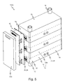
Figur 5 zeigt eine dreidimensionale Ansicht einer ersten Ausgestaltung der erfindungsgemäßen Anordnung. -
Figur 6 zeigt eine dreidimensionale Ansicht einer zweiten Ausgestaltung der erfindungsgemäßen Anordnung.
-
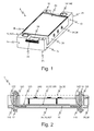
FIG. 1 shows a three-dimensional view of a power semiconductor module of an inventive arrangement. -
FIG. 2 schematically shows a plan view from the direction of a longitudinal side to a section through a power semiconductor module of an inventive arrangement. -
FIG. 3 shows a plan view from the direction of a main page on a power semiconductor module according to the invention without housing or on a corresponding capacitor device. -
FIG. 4 shows in the upper part a schematic plan view from the direction of a longitudinal side to a section through a power semiconductor sub-module and in the lower part of a corresponding plan view of a capacitor device of the arrangement according to the invention. -
FIG. 5 shows a three-dimensional view of a first embodiment of the inventive arrangement. -
FIG. 6 shows a three-dimensional view of a second embodiment of the inventive arrangement.
Ebenfalls dargestellt ist ein Gehäuse 30 des Leistungshalbleitermoduls 1, das die Ausnehmung der U-förmig ausgebildeten Kühleinrichtung 10 überdeckt und dabei wesentliche Teile der ersten Hauptseite 2a ausbildet. Durch das Gehäuse 30 überdeckt und nicht sichtbar ist die leistungselektronische Schaltung 22 der leistungselektronischen Schalteinrichtung 20 des Leistungshalbleitermoduls 1 angeordnet. Von der leistungselektronischen Schalteinrichtung 20 sichtbar sind Lastanschlusseinrichtungen 24, 26, hier Lastausgangsanschlusseinrichtungen 26, sowie Steueranschlusseinrichtungen 28. Diese durchdringen das Gehäuse 30 an jeweils zugeordneten Ausnehmungen 34, 36, 38, die Lastanschlusseinrichtungen 24, 26 an Längs- 3a /b, die Steueranschlusseinrichtungen 28 an einer Schmalseite 4a des Leistungshalbleitermoduls 1.Also shown is a
Die Kühlflüssigkeit des Vorlaufs 12 gelangt bei dem Leistungshalbleitermodul 1 durch einen Vorlaufzufluss 110 an der zweiten Hauptseite 2b in die Kühleinrichtung 10 und wird dort mittels eines ersten Abzweigs 122 in zwei Teilströme aufgeteilt. Der wesentliche Teil der Kühlflüssigkeit verlässt die Kühleinrichtung 10 des Leistungshalbleitermoduls 1 durch den Vorlaufabfluss 120 an der ersten Hauptseite 2a, während ein kleinerer Anteil der Kühlflüssigkeit das Kühlvolumen 16 mit angrenzender Kühlfläche 160 durchströmt.The cooling liquid of the
An der ersten Hauptfläche 2a ist der Rücklaufzufluss 130 angeordnet. Die Kühlflüssigkeit des Rücklaufs 14 gelangt durch diesen in die Kühleinrichtung 10 und vereinigt sich an einem zweiten Abzweig 142 mit der Kühlflüssigkeit die das Kühlvolumen 16 durchströmt hat. Der Rücklauf 14 verlässt die Kühleinrichtung 10 danach durch den Rücklaufabfluss 140 auf der zweiten Hauptseite 2b.At the first
Zusätzlich weist dieses Leistungshalbleitermodul 1 noch eine interne Steuerplatine 240 auf, die in fachüblicher Weise mit den Schaltmodulen 220 und mit dort angeordneten Leistungshalbleiterbauelementen schaltungsgerecht verbunden ist und Treiberfunktionalität für die leistungselektronische Schaltung 22 bereitstellt. Diese interne Steuerplatine 240 weist als Teil der leistungselektronischen Schalteinrichtung 20 an einer Schmalseite 4a des Leistungshalbleitermoduls 1 eine Steueranschlusseinrichtung 28 auf, die durch eine Ausnehmung 38 des Gehäuses 30 ragt.In addition, this
Dargestellt ist hier wiederum eine U-förmige Kühleinrichtung 10 mit einem Vorlaufabfluss 120 und einem Rücklaufabfluss 140 in gegenüberliegenden Ecken der ersten Hauptseite 2a. Zusätzlich sind in allen Ecken der Kühleinrichtung 10 von erster 2a zu zweiter Hauptseite 2b hindurchreichende nicht mit dem Kühlreislauf verbundene Ausnehmungen 18 vorgesehen, die der Verbindung zu weiteren Leistungshalbleitermodulen dienen, indem hierdurch Schraubverbindungen zur Verbindung der Leistungshalbleitermodule zu einer erfindungsgemäßen Anordnung anordenbar sind.Shown here is again a
Weiterhin dargestellt ist eine Kühlfläche 160 auf der drei Schaltmodule 220 der leistungselektronischen Schaltung 22 angeordnet sind. Die von diesen Submodulen 220 zu den Längsseiten 3 a/b reichenden Lastanschlusseinrichtungen 24, 26 sind ebenso wie die von diesen Submodulen 220 zu einer Schmalseite 4 a/b reichende Hilfsanschlusseinrichtung 28 nicht dargestellt.Also shown is a
Die Kondensatoreinrichtung 50 mit direkter Kühlung ist bezüglich der Ausgestaltung der Kühleinrichtung identisch zum Leistungshalbleitermodul ausgebildet. Anstelle der Schaltmodule des Leistungshalbleitermoduls sind bei der Kondensatoreinrichtung drei, gestrichelt dargestellte, Kondensatoren 58 vorgesehen. Lastanschlusseinrichtungen der Kondensatoreinrichtung sind nicht dargestellt, können allerdings an der ersten Längsseite 3a vorgesehen sein.The
Das Leistungshalbleiterteilmodul 1 b weist wiederum eine Kühleinrichtung 10 analog derjenigen des Leistungshalbleitermoduls gemäß
Diese integrierte Kondensatoreinrichtung 50b weist ebenso wie das Leistungshalbleiterteilmodul 1 b eine quaderförmige Grundform auf. Weiterhin weist die integrierte Kondensatoreinrichtung 50b eine eigene Kühleinrichtung 500 zur direkten Kühlung auf, die analog derjenigen des Leistungshalbleiterteilmoduls 1 b einen Vorlaufzufluss 510 und einen Rücklaufzufluss 530 auf der zweiten Hauptseite 502b aufweist.This
In einer weiteren bevorzugten Ausführung sind bei dem integrierten Leistungshalbleiterteilmodul 1 b mit integrierter Kondensatoreinrichtung 50b die beiden Kühleinrichtungen 10, 500 des Leistungshalbleiterteilmoduls 1 b und der integrierten Kondensatoreinrichtung 50b quasi einstückig ausgebildet. Hierunter soll verstanden werden, dass bei der Ausgestaltung gemäß dieses Ausführungsbeispiels ohne Beschränkung der Allgemeinheit der Vorlaufabfluss 520 der Kühleinrichtung 500 der integrierten Kondensatoreinrichtung 50b mit dem Vorlaufzufluss 110 der Kühleinrichtung 10 des Leistungshalbleiterteilmoduls 1 b und der Rücklaufabfluss 540 der integrierten Kondensatoreinrichtung 50b mit dem Rücklaufzufluss 130 des Leistungshalbleiterteilmoduls 1 b ohne dort vorgesehene zusätzliche Dichtmittels einstückig miteinander verbunden sind. Dies bedeutet nicht zwangsläufig, dass die jeweiligen Kühleinrichtungen10, 500 bzw. die daraus gebildete gemeinsame Kühleinrichtung intrinsisch ebenfalls einstückig ausgebildet sein müssen.In a further preferred embodiment, in the integrated
Die Kühlflüssigkeit des Vorlaufs 12 gelangt bei dem integrierten Leistungshalbleitermodul 1a durch einen Vorlaufzufluss 110 an der zweiten Hauptseite 502b in die Kühleinrichtung 10 und wird dort mittels eines zweiten Abzweigs 522 in zwei Teilströme aufgeteilt. Der wesentliche Teil der Kühlflüssigkeit fließt weiter zu einem ersten Abzweig 122 wird dort wiederum geteilt und verlässt die Kühleinrichtung 10 des integrierten Leistungshalbleiterteilmoduls 1 b durch den Vorlaufabfluss 120 an der ersten Hauptseite 2a, während jeweils ein kleinerer Anteil der Kühlflüssigkeit die Kühlvolumina 16, 56 mit angrenzenden Kühlflächen 160, 162, 560 durchströmt.In the case of the integrated
Auf der Kühlfläche 560 der Kühleinrichtung 500 der integrierte Kondensatoreinrichtung 50b sind hier drei Kondensatoren 58 angeordnet und mit der zweiten Kühlfläche 162 des Leistungshalbleiterteilmoduls 1 b und mit der Kühlfläche 560 der integrierten Kondensatoreinrichtung 50b in thermischem Kontakt. Somit ist es sichergestellt, dass die Kondensatoren 58 einen hervorragenden thermischen Kontakt zur Kühlflüssigkeit aufweisen. Dies ist insbesondere notwendig, da häufig die thermische Belastbarkeit der Kondensatoren 58 geringer ist als diejenige der Leistungshalbleiterbauelemente der Schaltmodule 220.Three
Die leistungselektronische Schalteinrichtung 20 des Leistungshalbleiterteilmoduls 1b ist grundsätzlich gleichartig derjenigen des Leistungshalbleitermoduls gemäß
Bei dieser vorteilhaften Ausgestaltung werden die Hauptseiten des integrierten Leistungshalbleitermoduls 1 a gebildet aus der ersten Hauptseite 2a des Leistungshalbleiterteilmoduls 1 b und der zweiten Hauptseite 502b der integrierten Kondensatoreinrichtung 50b. Die zweite Hauptseite 2b des Leistungshalbleiterteilmoduls 1 b bildet hierbei quasi nur die zweite Kühlfläche 162 des Leistungshalbleiterteilmoduls 1 b aus, während die erste Hauptfläche 502a der Kondensatoreinrichtung im Wesentlichen durch die Oberfläche der zu kühlenden Kondensatoren 58 gebildet wird.In this advantageous embodiment, the main sides of the integrated
Die integrierten Leistungshalbleitermodule 1a sind unmittelbar unter Verwendung von geeigneten Dichteinrichtungen miteinander verbunden. Sie liegen somit direkt aneinander an oder weisen nur einen geringen Abstand voneinander auf. Zur Ausbildung der Anordnung 100a sind die jeweiligen integrierten Leistungshalbleitermodule 1a mittels einer nicht dargestellten Klemmeinrichtung miteinander verbunden. Ebenso können die jeweiligen Leistungshalbleitermodule 1 a mittels Schraubverbindungen, vgl.
Die Anordnung weist jeweils einen gemeinsamen Vor- 12 und Rücklauf 14 für die Kühlflüssigkeit auf. Jedes der Leistungshalbleitermodule 1a weist auf der gleichen hier sichtbaren ersten Längsseite 3a Lasteingangsanschlusseinrichtungen 24, die hier als Gleichspannungsanschlusseinrichtungen ausgebildet sind, auf, die durch Ausnehmungen 34 des Gehäuses 30 hindurchragen. Die Wechselspannungsanschlusseinrichtungen, die Lastausgangsanschlusseinrichtungen, der mit den leistungselektronischen Schalteinrichtungen der Leistungshalbleitermodule 1a hier realisierten Wechselrichterschaltung sind auf den nicht sichtbaren zweiten Längsseiten angeordnet.The arrangement has in each case a
Die Hilfsanschlusseinrichtung 28 aller Leistungshalbleitermodule 1a der Anordnung 100a sind auf einer Schmalseite 4a der jeweiligen Leistungshalbleitermodule 1 a angeordnet. Dies hat den entscheidenden Vorteil, dass die Längsseiten 3 a/b für die Ausbildung der externen Lastverbindungen frei verfügbar sind. Somit ist eine besonders vorteilhafte, beispielsweise niederinduktive externe Verbindung mit dieser Anordnung 100a realisierbar.The auxiliary connection device 28 of all
Die Hilfsanschlusseinrichtungen 28 ragen durch zugeordnete Ausnehmungen 38 des Gehäuses 30 und sind hier mit einer gemeinsamen externen Steuerplatine 40 verbunden, die verschiedene Funktionalität aufweisen kann. Sie kann nur der Signalverbindung dienen aber auch komplexe Steuer- und Überwachungsfunktionalität aufweisen. In der hier gezeigten Ausfertigung weist die externe Steuerplatine 40 noch eine Dichteinrichtung 400 auf um gegen Umwelteinflüsse geschützt zu sein. Dies ist insbesondere in Kombination mit staub- und feuchtigkeitsdicht verkapselten integrierten Leistungshalbleitermodulen 1a vorteilhaft.The auxiliary terminal devices 28 protrude through associated
Diese Verbindung kann unmittelbar oder mittelbar, also unter Zwischenschaltung von Verbindungsstücken, ausgebildet sein. Jeweils sind selbstverständlich geeignete Dichteinrichtungen in beiden Varianten fachüblich vorzusehen.This connection can be formed directly or indirectly, ie with the interposition of connecting pieces. In each case, of course, suitable sealing devices in both variants are provided in the usual way.
Die jeweiligen Kondensatoreinrichtungen 50 weisen keine eigenen Kühleinrichtungen auf und sind somit über Kühlflächen 162 der Leistungshalbleitermodule 1 ausschließlich indirekt gekühlt.The
Ebenso sind hier Lastanschlusseinrichtungen 524 der Kondensatoreinrichtung 50 in Normalenrichtung der Hauptflächen 2 a/b fluchtend zu zugeordneten Lasteingangsanschlusseinrichtungen 24 der Leistungshalbleitermodule 1 dargestellt. Diese ermöglicht eine besonders einfache Verbindung von externen Anschlusseinrichtungen gleicher Polarität. An den zweiten nicht sichtbaren Längsseiten sind die Lastausgangsanschlusseinrichtungen der Leistungshalbleitermodule 1 angeordnet. Hilfsanschlusseinrichtungen sind hier nicht dargestellt aber selbstverständlich an den Schmalseiten der Leistungshalbleitermodule vorsehbar.Likewise,
Claims (14)
und wobei die Leistungshalbleitermodule (1) mit ihren Hauptseiten (2 a/b) aneinandergereiht sind, indem korrespondierende Anschlusseinrichtungen (110, 120, 130, 140) aufeinanderfolgender Leistungshalbleitermodule (1) mittelbar oder unmittelbar miteinander verbunden sind und wobei zwischen mindestens zwei aufeinanderfolgenden Leistungshalbleitermodulen (1) eine Kondensatoreinrichtung (50) angeordnet ist, die ihrerseits mittels des Kühlkreislaufes der Anordnung direkt oder indirekt gekühlt wird.Arrangement (100) with a cooling circuit, a plurality of stackable power semiconductor modules (1) and at least one capacitor device (50), wherein a power semiconductor module (1) has a power electronic switching device (20) and a flow-through cooling device (10) for cooling the switching device (20) comprising a cooling volume (16) at least one cooling surface (160, 162) and four connection means (110, 120, 130, 140) for a cooling liquid, wherein the connection means (110, 120, 130, 140) in pairs on main sides (2 a / b) of the power semiconductor module (1) are arranged,
and wherein the power semiconductor modules (1) are lined up with their main sides (2 a / b) by directly or indirectly interconnecting corresponding connection devices (110, 120, 130, 140) of successive power semiconductor modules (1) and between at least two successive power semiconductor modules ( 1) a capacitor device (50) is arranged, which in turn is cooled directly or indirectly by means of the cooling circuit of the arrangement.
das Leistungshalbleitermodul (1) eine leistungselektronische Schalteinrichtung (20) mit einer leistungselektronischen Schaltung (22), Steuer- (28), Lasteingangs- (24) und Lastausgangsanschlusseinrichtungen (26) und vorzugsweise ein Gehäuse (30) mit Ausnehmungen (34, 36, 38) für diese Anschlusseinrichtungen (110, 120, 130, 140) aufweist, und hierbei das Gehäuse (30) die leistungselektronische Schaltung (22) zur die Kühleinrichtung (10) hin überdeckt.Arrangement according to claim 1, wherein
the power semiconductor module (1) has a power electronic switching device (20) with a power electronic circuit (22), control (28), load input (24) and load output terminal devices (26) and preferably a housing (30) with recesses (34, 36, 38 ) for this connection means (110, 120, 130, 140), and in this case the housing (30) covers the power electronic circuit (22) to the cooling device (10) out.
die Kondensatoreinrichtung (50) Lastanschlusseinrichtungen (524) aufweist und diese schaltungsgerecht mit zugeordneten Lasteingangs- (24) oder Lastausgangsanschlusseinrichtungen (26) mindestens eines Leistungshalbleitermoduls (1) verbunden sind.Arrangement according to claim 2, wherein
the capacitor device (50) has load connection devices (524) and these are connected in a circuit-compatible manner to assigned load input (24) or load output connection devices (26) of at least one power semiconductor module (1).
bei den jeweiligen Leistungshalbleitermodulen (1) der Vorlaufzufluss (110) und der Rücklaufabfluss (140), sowie der Vorlaufabfluss (120) und der Rücklaufzufluss (130) jeweils auf einer Hauptseite (2 a/b) oder wobei der Vorlaufzufluss (110) und der Rücklaufzufluss (130), sowie der Vorlaufabfluss (120) und der Rücklaufabfluss (140) jeweils auf einer Hauptseite (2 a/b) angeordnet sind.Arrangement according to claim 4, wherein
in the respective power semiconductor modules (1) the flow inlet (110) and the return flow (140), and the flow discharge (120) and the return flow (130) respectively on a main side (2 a / b) or wherein the flow inlet (110) and the Return flow (130), and the flow discharge (120) and the return flow (140) are each arranged on a main side (2 a / b).
der Vorlaufabfluss (120) eines Leistungshalbleitermoduls (1) mit dem Vorlaufzufluss (110) und der Rücklaufzufluss (130) mit dem Rücklaufabfluss (140) des nachfolgenden Leistungshalbleitermoduls (1) mittelbar oder unmittelbar verbunden sind oder
wobei die Leistungshalbleitermodule (1) aneinandergereiht sind, indem der Vorlaufabfluss (120) eines Leistungshalbleitermoduls mit dem Vorlaufzufluss (110) und der Rücklaufabfluss (140) mit dem Rücklaufzufluss (130) des nachfolgenden Leistungshalbleitermoduls mittelbar oder unmittelbar verbunden sind.Arrangement according to claim 5, wherein
the flow outlet (120) of a power semiconductor module (1) with the flow inlet (110) and the return flow (130) with the return flow (140) of the subsequent power semiconductor module (1) are connected directly or indirectly;
wherein the power semiconductor modules (1) are lined up by the feed flow (120) of a power semiconductor module with the feed flow (110) and the return flow (140) with the return flow (130) of the subsequent power semiconductor module are directly or indirectly connected.
das Leistungshalbleitermodul (1) zwischen dem Vorlaufzufluss (110) und dem Vorlaufabfluss (120) ein erster Abzweig (122) sowie zwischen Rücklaufzufluss (130) und Rücklaufabfluss (140) ein zweiter Abzweig (142) angeordnet sind, wodurch das Kühlvolumen (16) der Kühleinrichtung (10) mit Kühlflüssigkeit von einem Vorlauf (12) zu einem Rücklauf (14) durchströmbar ist.Arrangement according to claim 4, wherein
the power semiconductor module (1) between the feed flow (110) and the feed outflow (120) a first branch (122) and between the return flow (130) and return flow (140) a second branch (142) are arranged, whereby the cooling volume (16) of Cooling device (10) with coolant from a flow (12) to a return (14) can be flowed through.
die Kondensatoreinrichtung (50) in thermisch leitendem Kontakt mit einer Kühlfläche (160, 162) eines oder beider benachbarter Leistungshalbleitermodule (1) steht und die korrespondierenden Anschlusseinrichtungen (110, 120, 130, 140) benachbarter Leistungshalbleitermodule unmittelbar miteinander verbunden sind.Arrangement according to claim 1, wherein
the capacitor device (50) in thermally conductive contact with a cooling surface (160, 162) of one or both adjacent power semiconductor modules (1) and the corresponding connection devices (110, 120, 130, 140) of adjacent power semiconductor modules are connected directly to each other.
die Kondensatoreinrichtung (50) eigene zweite Anschlusseinrichtungen (510, 520, 530, 540) aufweist, die jeweils als ein Vorlaufzufluss (510) und ein Vorlaufabfluss (520) sowie als eine Rücklaufzufluss (530) und ein Rücklaufabfluss (540) ausgebildet sind und die korrespondierenden Anschlusseinrichtungen (110, 120, 130, 140) benachbarter Leistungshalbleitermodule mittelbar miteinander verbunden sind indem die Kondensatoreinrichtung (50) in Bezug auf den Kühlkreislauf dazwischengeschaltet ist.Arrangement according to claim 1, wherein
the condenser device (50) has its own second connection devices (510, 520, 530, 540) which are each designed as a feed flow (510) and a feed outflow (520) and as a return flow (530) and a return flow (540) and corresponding terminal devices (110, 120, 130, 140) of adjacent power semiconductor modules are indirectly connected to each other by the capacitor device (50) is interposed with respect to the cooling circuit.
die Kondensatoreinrichtung (50) durchströmbar für die Kühlflüssigkeit ausgebildet ist und somit ein zweites Kühlvolumen (56) sowie zu dessen Durchströmung zwei dem Vor- (12) bzw. Rücklauf (14) zugeordnete Abzweige (522, 542) aufweist.Arrangement according to claim 1, wherein
the capacitor device (50) is designed to flow through for the cooling liquid and thus has a second cooling volume (56) and to the flow through two of the pre (12) and return (14) associated branches (522, 542).
und wobei die integrierten Leistungshalbleitermodule (1a) mit ihren Hauptseiten (2a, 502b) anreihbar sind indem korrespondierende Anschlusseinrichtungen (510, 120, 530, 140) aufeinanderfolgender integrierter Leistungshalbleitermodule (1 b) miteinander verbindbar sind.Integrated power semiconductor module (1a) with integrated capacitor device (50b) and a common housing (30), wherein the integrated power semiconductor module (1a) has a power semiconductor sub-module (1 b), a power electronic switching device (20) and a flow-through cooling device (10, 500) for this purpose comprising at least one cooling volume (16, 56) for cooling the power electronic circuit (22) and capacitors (58) of the integrated capacitor device (50b) and four cooling fluid connection devices (510, 120, 530, 140) in pairs Main sides (2a, 502b) of the integrated power semiconductor module (1a) are arranged,
and wherein the integrated power semiconductor modules (1a) can be arranged with their main sides (2a, 502b) by connecting corresponding connection devices (510, 120, 530, 140) of successive integrated power semiconductor modules (1b) to one another.
und wobei die integrierten Leistungshalbleitermodule (1a) mit ihren Hauptseiten (2a, 502b) aneinandergereiht sind indem korrespondierende Anschlusseinrichtungen (510, 120, 530, 140) aufeinanderfolgender integrierter Leistungshalbleitermodule (1a) unmittelbar miteinander verbunden sind.Arrangement (100a) having a cooling circuit, a plurality of stackable integrated power semiconductor modules (1a) with a power semiconductor sub-module (1b) and an integrated capacitor device (50b), wherein the integrated power semiconductor module (1a) comprises a power electronic switching device (20) and a flow-through cooling device (10 , 500), which has a cooling volume (16, 56) at least one cooling surface (160, 162, 560) and four connection devices (510, 120, 530, 140) for the cooling liquid, which are in pairs on main sides (2 a / b) the integrated power semiconductor module (1a) are arranged,
and wherein the integrated power semiconductor modules (1a) are lined up with their main sides (2a, 502b) in that corresponding connection devices (510, 120, 530, 140) of successive integrated power semiconductor modules (1a) are directly connected to one another.
Applications Claiming Priority (1)
| Application Number | Priority Date | Filing Date | Title |
|---|---|---|---|
| DE102012206271A DE102012206271A1 (en) | 2012-04-17 | 2012-04-17 | Liquid-cooled arrangement with storable power semiconductor modules and at least one capacitor device and power semiconductor module for this purpose |
Publications (3)
| Publication Number | Publication Date |
|---|---|
| EP2654391A2 true EP2654391A2 (en) | 2013-10-23 |
| EP2654391A3 EP2654391A3 (en) | 2017-02-15 |
| EP2654391B1 EP2654391B1 (en) | 2018-11-28 |
Family
ID=47681758
Family Applications (1)
| Application Number | Title | Priority Date | Filing Date |
|---|---|---|---|
| EP13154128.6A Not-in-force EP2654391B1 (en) | 2012-04-17 | 2013-02-06 | Liquid-cooled assembly with in-line power semiconductor modules and at least one capacitor device and power semiconductor module therefor |
Country Status (6)
| Country | Link |
|---|---|
| US (1) | US9165858B2 (en) |
| EP (1) | EP2654391B1 (en) |
| JP (1) | JP2013222974A (en) |
| KR (1) | KR20130117671A (en) |
| CN (2) | CN103378027B (en) |
| DE (1) | DE102012206271A1 (en) |
Families Citing this family (16)
| Publication number | Priority date | Publication date | Assignee | Title |
|---|---|---|---|---|
| DE102012206271A1 (en) * | 2012-04-17 | 2013-10-17 | Semikron Elektronik Gmbh & Co. Kg | Liquid-cooled arrangement with storable power semiconductor modules and at least one capacitor device and power semiconductor module for this purpose |
| FR3002624B1 (en) * | 2013-02-28 | 2015-02-27 | Bull Sas | HYDRAULIC DISTRIBUTOR |
| JP6233257B2 (en) * | 2014-04-15 | 2017-11-22 | トヨタ自動車株式会社 | Power converter |
| US10264695B2 (en) * | 2014-09-25 | 2019-04-16 | Hitachi Automotive Systems, Ltd. | Power converter |
| CN106816803B (en) * | 2015-11-27 | 2019-06-18 | 讯凯国际股份有限公司 | Pump module and its pumping |
| JP6929788B2 (en) | 2015-12-04 | 2021-09-01 | ローム株式会社 | Power module equipment and electric or hybrid vehicles |
| CN109216291B (en) * | 2017-06-29 | 2022-06-21 | 比亚迪半导体股份有限公司 | Radiator for power module and vehicle with radiator |
| DE102017212434A1 (en) * | 2017-07-20 | 2019-01-24 | Audi Ag | Electronic device with at least one component to be cooled |
| DE102018203362A1 (en) * | 2018-03-07 | 2019-09-12 | Robert Bosch Gmbh | Cooling device for cooling a power device |
| JP7052447B2 (en) * | 2018-03-16 | 2022-04-12 | 富士電機株式会社 | Power converter |
| JP7218828B2 (en) * | 2018-03-16 | 2023-02-07 | 富士電機株式会社 | power converter |
| CN110986651B (en) * | 2019-12-10 | 2021-11-02 | 常州大学 | Finned tube heat exchanger with heat exchange cavity in fin |
| KR20210076689A (en) | 2019-12-16 | 2021-06-24 | 삼성전자주식회사 | Heat exchanger module, assembly type heat exchanger comprising heat exchanger module and assembly system of heat exchanger |
| US10912231B1 (en) | 2020-01-15 | 2021-02-02 | Ford Global Technologies, Llc | Automotive integrated power module and capacitor |
| US11502349B2 (en) | 2020-08-31 | 2022-11-15 | Borgwarner, Inc. | Cooling manifold assembly |
| DE102022201329A1 (en) | 2022-02-09 | 2023-08-10 | Zf Friedrichshafen Ag | Switch module for an inverter, inverter with several such switch modules and vehicle with the inverter |
Citations (2)
| Publication number | Priority date | Publication date | Assignee | Title |
|---|---|---|---|---|
| DE10316356A1 (en) | 2003-04-10 | 2004-11-11 | Semikron Elektronik Gmbh | Modular power semiconductor module |
| EP1815514B1 (en) | 2004-11-24 | 2008-04-23 | Danfoss Silicon Power GmbH | A flow distribution module and a stack of flow distribution modules |
Family Cites Families (21)
| Publication number | Priority date | Publication date | Assignee | Title |
|---|---|---|---|---|
| US5053856A (en) * | 1990-09-04 | 1991-10-01 | Sun Microsystems, Inc. | Apparatus for providing electrical conduits in compact arrays of electronic circuitry utilizing cooling devices |
| FR2765067B1 (en) * | 1997-06-19 | 1999-07-16 | Alsthom Cge Alcatel | POWER ELECTRONICS MODULE AND POWER ELECTRONICS DEVICE PROVIDED WITH SUCH MODULES |
| JP4423746B2 (en) * | 2000-05-10 | 2010-03-03 | 株式会社デンソー | Refrigerant cooling type double-sided cooling semiconductor device |
| JP4009056B2 (en) * | 2000-05-25 | 2007-11-14 | 三菱電機株式会社 | Power module |
| EP2216891B1 (en) * | 2003-08-21 | 2012-01-04 | Denso Corporation | Mounting structure ofa semiconductor device |
| JP4225310B2 (en) * | 2004-11-11 | 2009-02-18 | 株式会社デンソー | Semiconductor device |
| US8125781B2 (en) * | 2004-11-11 | 2012-02-28 | Denso Corporation | Semiconductor device |
| JP4661645B2 (en) * | 2005-03-23 | 2011-03-30 | トヨタ自動車株式会社 | Power semiconductor module |
| CN101146429A (en) * | 2006-09-15 | 2008-03-19 | 刘胜 | Radiator of electronic device |
| JP4293246B2 (en) * | 2007-02-19 | 2009-07-08 | 株式会社日立製作所 | Power converter |
| JP4683003B2 (en) * | 2007-03-30 | 2011-05-11 | 株式会社デンソー | Power module and power converter using the same |
| JP2010135697A (en) * | 2008-12-08 | 2010-06-17 | Toyota Motor Corp | Lamination module structure |
| JP5212088B2 (en) * | 2008-12-25 | 2013-06-19 | 株式会社デンソー | Semiconductor module cooling device |
| JP5658435B2 (en) | 2009-03-31 | 2015-01-28 | リンテック株式会社 | Mask film member, mask film manufacturing method using the same, and photosensitive resin printing plate manufacturing method |
| JP4775475B2 (en) * | 2009-04-14 | 2011-09-21 | 株式会社デンソー | Power converter |
| US7952875B2 (en) * | 2009-05-29 | 2011-05-31 | GM Global Technology Operations LLC | Stacked busbar assembly with integrated cooling |
| JP5327195B2 (en) * | 2010-02-05 | 2013-10-30 | 株式会社デンソー | Power converter |
| JP5392196B2 (en) * | 2010-06-30 | 2014-01-22 | 株式会社デンソー | Semiconductor device |
| JP5115632B2 (en) * | 2010-06-30 | 2013-01-09 | 株式会社デンソー | Semiconductor device |
| CN103999213A (en) * | 2011-12-20 | 2014-08-20 | 丰田自动车株式会社 | Semiconductor module |
| DE102012206271A1 (en) * | 2012-04-17 | 2013-10-17 | Semikron Elektronik Gmbh & Co. Kg | Liquid-cooled arrangement with storable power semiconductor modules and at least one capacitor device and power semiconductor module for this purpose |
-
2012
- 2012-04-17 DE DE102012206271A patent/DE102012206271A1/en not_active Withdrawn
-
2013
- 2013-02-06 EP EP13154128.6A patent/EP2654391B1/en not_active Not-in-force
- 2013-04-05 KR KR1020130037368A patent/KR20130117671A/en not_active Application Discontinuation
- 2013-04-16 JP JP2013085613A patent/JP2013222974A/en active Pending
- 2013-04-16 CN CN201310130929.1A patent/CN103378027B/en not_active Expired - Fee Related
- 2013-04-16 CN CN201320191489.6U patent/CN203386739U/en not_active Withdrawn - After Issue
- 2013-04-17 US US13/865,184 patent/US9165858B2/en not_active Expired - Fee Related
Patent Citations (2)
| Publication number | Priority date | Publication date | Assignee | Title |
|---|---|---|---|---|
| DE10316356A1 (en) | 2003-04-10 | 2004-11-11 | Semikron Elektronik Gmbh | Modular power semiconductor module |
| EP1815514B1 (en) | 2004-11-24 | 2008-04-23 | Danfoss Silicon Power GmbH | A flow distribution module and a stack of flow distribution modules |
Also Published As
| Publication number | Publication date |
|---|---|
| EP2654391A3 (en) | 2017-02-15 |
| US9165858B2 (en) | 2015-10-20 |
| DE102012206271A1 (en) | 2013-10-17 |
| CN203386739U (en) | 2014-01-08 |
| JP2013222974A (en) | 2013-10-28 |
| CN103378027B (en) | 2018-11-02 |
| US20130271917A1 (en) | 2013-10-17 |
| EP2654391B1 (en) | 2018-11-28 |
| KR20130117671A (en) | 2013-10-28 |
| CN103378027A (en) | 2013-10-30 |
Similar Documents
| Publication | Publication Date | Title |
|---|---|---|
| EP2654391B1 (en) | Liquid-cooled assembly with in-line power semiconductor modules and at least one capacitor device and power semiconductor module therefor | |
| EP2654392B1 (en) | In-line liquid cooled semiconductor module and assembly with the same | |
| EP2272311B1 (en) | Cooling device for a plurality of power modules | |
| EP2364581B1 (en) | Rectifier module with cooled busbar | |
| EP1848260B1 (en) | Inverter | |
| EP2458633A2 (en) | Power semiconductor | |
| DE102005034998B4 (en) | Method for producing a device for cooling electronic components and device for cooling electronic components | |
| DE202012012767U1 (en) | Power semiconductor module system | |
| WO2012152551A1 (en) | Power electronic system having a liquid cooling device | |
| EP2528091A2 (en) | High performance electronic system with subsystem and a cooling device | |
| EP2521432A2 (en) | High performance electronics assembly with liquid cooling | |
| DE102012215787B4 (en) | Power electronic system with liquid cooling device and vehicle with it | |
| DE102016103788A1 (en) | Plastic cooler for semiconductor modules | |
| EP3328678A1 (en) | Traction battery for a motor vehicle, comprising a cooling device | |
| DE102005031759A1 (en) | Converter arrangement for use in dynamically controlled motor, has cooling device comprising metallic mold bodies, and cooling surfaces formed with cooling units, where cooling medium e.g. air, flows through cooling device | |
| DE102017005315A1 (en) | battery box | |
| DE112018000105T5 (en) | ELECTRONIC COMPONENT AND POWER CONVERSION DEVICE | |
| DE102012220280A1 (en) | Electronic housing for modular electronics housing system and modular converter system in e.g. vehicle, has first and second flanges provided with portions of first recess-projection connection and second recess-projection connection | |
| DE102008058032A1 (en) | Microstructure fluid cooler for e.g. CPU of personal computer, has base plate and intermediate levels produced by etching process, where material strength and remaining base thickness utilized by etching process amounts to specific values | |
| EP3762964A1 (en) | Cooling device for cooling a power component | |
| EP1739804A1 (en) | Rail for electrically conductive support of one or more electrical devices | |
| EP1758165B1 (en) | Power semiconductor module with means for mounting on a heatsink | |
| DE102018209548A1 (en) | Capacitor carrier unit for opening / closing a module | |
| DE102011100524B4 (en) | Power electronic arrangement | |
| DE102007003920A1 (en) | Liquid radiator for one or multiple electrical or electronic units, has lower cooling plate and upper cooling plate, where one or multiple cooling units are arranged and coolant channels are designed as slots |
Legal Events
| Date | Code | Title | Description |
|---|---|---|---|
| PUAI | Public reference made under article 153(3) epc to a published international application that has entered the european phase |
Free format text: ORIGINAL CODE: 0009012 |
|
| AK | Designated contracting states |
Kind code of ref document: A2 Designated state(s): AL AT BE BG CH CY CZ DE DK EE ES FI FR GB GR HR HU IE IS IT LI LT LU LV MC MK MT NL NO PL PT RO RS SE SI SK SM TR |
|
| AX | Request for extension of the european patent |
Extension state: BA ME |
|
| PUAL | Search report despatched |
Free format text: ORIGINAL CODE: 0009013 |
|
| AK | Designated contracting states |
Kind code of ref document: A3 Designated state(s): AL AT BE BG CH CY CZ DE DK EE ES FI FR GB GR HR HU IE IS IT LI LT LU LV MC MK MT NL NO PL PT RO RS SE SI SK SM TR |
|
| AX | Request for extension of the european patent |
Extension state: BA ME |
|
| RIC1 | Information provided on ipc code assigned before grant |
Ipc: H01L 23/473 20060101ALI20170112BHEP Ipc: H05K 7/20 20060101AFI20170112BHEP Ipc: H01L 25/07 20060101ALI20170112BHEP Ipc: H01L 25/11 20060101ALI20170112BHEP |
|
| STAA | Information on the status of an ep patent application or granted ep patent |
Free format text: STATUS: REQUEST FOR EXAMINATION WAS MADE |
|
| 17P | Request for examination filed |
Effective date: 20170816 |
|
| RBV | Designated contracting states (corrected) |
Designated state(s): AL AT BE BG CH CY CZ DE DK EE ES FI FR GB GR HR HU IE IS IT LI LT LU LV MC MK MT NL NO PL PT RO RS SE SI SK SM TR |
|
| GRAP | Despatch of communication of intention to grant a patent |
Free format text: ORIGINAL CODE: EPIDOSNIGR1 |
|
| STAA | Information on the status of an ep patent application or granted ep patent |
Free format text: STATUS: GRANT OF PATENT IS INTENDED |
|
| INTG | Intention to grant announced |
Effective date: 20180903 |
|
| GRAS | Grant fee paid |
Free format text: ORIGINAL CODE: EPIDOSNIGR3 |
|
| GRAA | (expected) grant |
Free format text: ORIGINAL CODE: 0009210 |
|
| STAA | Information on the status of an ep patent application or granted ep patent |
Free format text: STATUS: THE PATENT HAS BEEN GRANTED |
|
| AK | Designated contracting states |
Kind code of ref document: B1 Designated state(s): AL AT BE BG CH CY CZ DE DK EE ES FI FR GB GR HR HU IE IS IT LI LT LU LV MC MK MT NL NO PL PT RO RS SE SI SK SM TR |
|
| REG | Reference to a national code |
Ref country code: GB Ref legal event code: FG4D Free format text: NOT ENGLISH |
|
| REG | Reference to a national code |
Ref country code: CH Ref legal event code: EP |
|
| REG | Reference to a national code |
Ref country code: AT Ref legal event code: REF Ref document number: 1071846 Country of ref document: AT Kind code of ref document: T Effective date: 20181215 |
|
| REG | Reference to a national code |
Ref country code: DE Ref legal event code: R096 Ref document number: 502013011689 Country of ref document: DE |
|
| REG | Reference to a national code |
Ref country code: IE Ref legal event code: FG4D Free format text: LANGUAGE OF EP DOCUMENT: GERMAN |
|
| REG | Reference to a national code |
Ref country code: NL Ref legal event code: MP Effective date: 20181128 |
|
| REG | Reference to a national code |
Ref country code: LT Ref legal event code: MG4D |
|
| PG25 | Lapsed in a contracting state [announced via postgrant information from national office to epo] |
Ref country code: IS Free format text: LAPSE BECAUSE OF FAILURE TO SUBMIT A TRANSLATION OF THE DESCRIPTION OR TO PAY THE FEE WITHIN THE PRESCRIBED TIME-LIMIT Effective date: 20190328 Ref country code: FI Free format text: LAPSE BECAUSE OF FAILURE TO SUBMIT A TRANSLATION OF THE DESCRIPTION OR TO PAY THE FEE WITHIN THE PRESCRIBED TIME-LIMIT Effective date: 20181128 Ref country code: LV Free format text: LAPSE BECAUSE OF FAILURE TO SUBMIT A TRANSLATION OF THE DESCRIPTION OR TO PAY THE FEE WITHIN THE PRESCRIBED TIME-LIMIT Effective date: 20181128 Ref country code: HR Free format text: LAPSE BECAUSE OF FAILURE TO SUBMIT A TRANSLATION OF THE DESCRIPTION OR TO PAY THE FEE WITHIN THE PRESCRIBED TIME-LIMIT Effective date: 20181128 Ref country code: NO Free format text: LAPSE BECAUSE OF FAILURE TO SUBMIT A TRANSLATION OF THE DESCRIPTION OR TO PAY THE FEE WITHIN THE PRESCRIBED TIME-LIMIT Effective date: 20190228 Ref country code: BG Free format text: LAPSE BECAUSE OF FAILURE TO SUBMIT A TRANSLATION OF THE DESCRIPTION OR TO PAY THE FEE WITHIN THE PRESCRIBED TIME-LIMIT Effective date: 20190228 Ref country code: ES Free format text: LAPSE BECAUSE OF FAILURE TO SUBMIT A TRANSLATION OF THE DESCRIPTION OR TO PAY THE FEE WITHIN THE PRESCRIBED TIME-LIMIT Effective date: 20181128 Ref country code: LT Free format text: LAPSE BECAUSE OF FAILURE TO SUBMIT A TRANSLATION OF THE DESCRIPTION OR TO PAY THE FEE WITHIN THE PRESCRIBED TIME-LIMIT Effective date: 20181128 |
|
| PG25 | Lapsed in a contracting state [announced via postgrant information from national office to epo] |
Ref country code: PT Free format text: LAPSE BECAUSE OF FAILURE TO SUBMIT A TRANSLATION OF THE DESCRIPTION OR TO PAY THE FEE WITHIN THE PRESCRIBED TIME-LIMIT Effective date: 20190328 Ref country code: RS Free format text: LAPSE BECAUSE OF FAILURE TO SUBMIT A TRANSLATION OF THE DESCRIPTION OR TO PAY THE FEE WITHIN THE PRESCRIBED TIME-LIMIT Effective date: 20181128 Ref country code: SE Free format text: LAPSE BECAUSE OF FAILURE TO SUBMIT A TRANSLATION OF THE DESCRIPTION OR TO PAY THE FEE WITHIN THE PRESCRIBED TIME-LIMIT Effective date: 20181128 Ref country code: GR Free format text: LAPSE BECAUSE OF FAILURE TO SUBMIT A TRANSLATION OF THE DESCRIPTION OR TO PAY THE FEE WITHIN THE PRESCRIBED TIME-LIMIT Effective date: 20190301 Ref country code: AL Free format text: LAPSE BECAUSE OF FAILURE TO SUBMIT A TRANSLATION OF THE DESCRIPTION OR TO PAY THE FEE WITHIN THE PRESCRIBED TIME-LIMIT Effective date: 20181128 |
|
| PG25 | Lapsed in a contracting state [announced via postgrant information from national office to epo] |
Ref country code: NL Free format text: LAPSE BECAUSE OF FAILURE TO SUBMIT A TRANSLATION OF THE DESCRIPTION OR TO PAY THE FEE WITHIN THE PRESCRIBED TIME-LIMIT Effective date: 20181128 |
|
| PG25 | Lapsed in a contracting state [announced via postgrant information from national office to epo] |
Ref country code: IT Free format text: LAPSE BECAUSE OF FAILURE TO SUBMIT A TRANSLATION OF THE DESCRIPTION OR TO PAY THE FEE WITHIN THE PRESCRIBED TIME-LIMIT Effective date: 20181128 Ref country code: CZ Free format text: LAPSE BECAUSE OF FAILURE TO SUBMIT A TRANSLATION OF THE DESCRIPTION OR TO PAY THE FEE WITHIN THE PRESCRIBED TIME-LIMIT Effective date: 20181128 Ref country code: DK Free format text: LAPSE BECAUSE OF FAILURE TO SUBMIT A TRANSLATION OF THE DESCRIPTION OR TO PAY THE FEE WITHIN THE PRESCRIBED TIME-LIMIT Effective date: 20181128 Ref country code: PL Free format text: LAPSE BECAUSE OF FAILURE TO SUBMIT A TRANSLATION OF THE DESCRIPTION OR TO PAY THE FEE WITHIN THE PRESCRIBED TIME-LIMIT Effective date: 20181128 |
|
| REG | Reference to a national code |
Ref country code: DE Ref legal event code: R097 Ref document number: 502013011689 Country of ref document: DE |
|
| PG25 | Lapsed in a contracting state [announced via postgrant information from national office to epo] |
Ref country code: EE Free format text: LAPSE BECAUSE OF FAILURE TO SUBMIT A TRANSLATION OF THE DESCRIPTION OR TO PAY THE FEE WITHIN THE PRESCRIBED TIME-LIMIT Effective date: 20181128 Ref country code: SM Free format text: LAPSE BECAUSE OF FAILURE TO SUBMIT A TRANSLATION OF THE DESCRIPTION OR TO PAY THE FEE WITHIN THE PRESCRIBED TIME-LIMIT Effective date: 20181128 Ref country code: RO Free format text: LAPSE BECAUSE OF FAILURE TO SUBMIT A TRANSLATION OF THE DESCRIPTION OR TO PAY THE FEE WITHIN THE PRESCRIBED TIME-LIMIT Effective date: 20181128 Ref country code: SK Free format text: LAPSE BECAUSE OF FAILURE TO SUBMIT A TRANSLATION OF THE DESCRIPTION OR TO PAY THE FEE WITHIN THE PRESCRIBED TIME-LIMIT Effective date: 20181128 |
|
| REG | Reference to a national code |
Ref country code: CH Ref legal event code: PL |
|
| PLBE | No opposition filed within time limit |
Free format text: ORIGINAL CODE: 0009261 |
|
| STAA | Information on the status of an ep patent application or granted ep patent |
Free format text: STATUS: NO OPPOSITION FILED WITHIN TIME LIMIT |
|
| GBPC | Gb: european patent ceased through non-payment of renewal fee |
Effective date: 20190228 |
|
| PG25 | Lapsed in a contracting state [announced via postgrant information from national office to epo] |
Ref country code: LU Free format text: LAPSE BECAUSE OF NON-PAYMENT OF DUE FEES Effective date: 20190206 Ref country code: MC Free format text: LAPSE BECAUSE OF FAILURE TO SUBMIT A TRANSLATION OF THE DESCRIPTION OR TO PAY THE FEE WITHIN THE PRESCRIBED TIME-LIMIT Effective date: 20181128 Ref country code: SI Free format text: LAPSE BECAUSE OF FAILURE TO SUBMIT A TRANSLATION OF THE DESCRIPTION OR TO PAY THE FEE WITHIN THE PRESCRIBED TIME-LIMIT Effective date: 20181128 |
|
| 26N | No opposition filed |
Effective date: 20190829 |
|
| REG | Reference to a national code |
Ref country code: BE Ref legal event code: MM Effective date: 20190228 |
|
| REG | Reference to a national code |
Ref country code: IE Ref legal event code: MM4A |
|
| PG25 | Lapsed in a contracting state [announced via postgrant information from national office to epo] |
Ref country code: CH Free format text: LAPSE BECAUSE OF NON-PAYMENT OF DUE FEES Effective date: 20190228 Ref country code: LI Free format text: LAPSE BECAUSE OF NON-PAYMENT OF DUE FEES Effective date: 20190228 |
|
| PG25 | Lapsed in a contracting state [announced via postgrant information from national office to epo] |
Ref country code: GB Free format text: LAPSE BECAUSE OF NON-PAYMENT OF DUE FEES Effective date: 20190228 Ref country code: IE Free format text: LAPSE BECAUSE OF NON-PAYMENT OF DUE FEES Effective date: 20190206 |
|
| PG25 | Lapsed in a contracting state [announced via postgrant information from national office to epo] |
Ref country code: BE Free format text: LAPSE BECAUSE OF NON-PAYMENT OF DUE FEES Effective date: 20190228 Ref country code: FR Free format text: LAPSE BECAUSE OF NON-PAYMENT OF DUE FEES Effective date: 20190228 |
|
| PG25 | Lapsed in a contracting state [announced via postgrant information from national office to epo] |
Ref country code: TR Free format text: LAPSE BECAUSE OF FAILURE TO SUBMIT A TRANSLATION OF THE DESCRIPTION OR TO PAY THE FEE WITHIN THE PRESCRIBED TIME-LIMIT Effective date: 20181128 |
|
| REG | Reference to a national code |
Ref country code: AT Ref legal event code: MM01 Ref document number: 1071846 Country of ref document: AT Kind code of ref document: T Effective date: 20190206 |
|
| PG25 | Lapsed in a contracting state [announced via postgrant information from national office to epo] |
Ref country code: AT Free format text: LAPSE BECAUSE OF NON-PAYMENT OF DUE FEES Effective date: 20190206 |
|
| PGFP | Annual fee paid to national office [announced via postgrant information from national office to epo] |
Ref country code: DE Payment date: 20200229 Year of fee payment: 8 |
|
| PG25 | Lapsed in a contracting state [announced via postgrant information from national office to epo] |
Ref country code: MT Free format text: LAPSE BECAUSE OF FAILURE TO SUBMIT A TRANSLATION OF THE DESCRIPTION OR TO PAY THE FEE WITHIN THE PRESCRIBED TIME-LIMIT Effective date: 20181128 |
|
| PG25 | Lapsed in a contracting state [announced via postgrant information from national office to epo] |
Ref country code: CY Free format text: LAPSE BECAUSE OF FAILURE TO SUBMIT A TRANSLATION OF THE DESCRIPTION OR TO PAY THE FEE WITHIN THE PRESCRIBED TIME-LIMIT Effective date: 20181128 |
|
| PG25 | Lapsed in a contracting state [announced via postgrant information from national office to epo] |
Ref country code: HU Free format text: LAPSE BECAUSE OF FAILURE TO SUBMIT A TRANSLATION OF THE DESCRIPTION OR TO PAY THE FEE WITHIN THE PRESCRIBED TIME-LIMIT; INVALID AB INITIO Effective date: 20130206 |
|
| REG | Reference to a national code |
Ref country code: DE Ref legal event code: R119 Ref document number: 502013011689 Country of ref document: DE |
|
| PG25 | Lapsed in a contracting state [announced via postgrant information from national office to epo] |
Ref country code: DE Free format text: LAPSE BECAUSE OF NON-PAYMENT OF DUE FEES Effective date: 20210901 |
|
| PG25 | Lapsed in a contracting state [announced via postgrant information from national office to epo] |
Ref country code: MK Free format text: LAPSE BECAUSE OF FAILURE TO SUBMIT A TRANSLATION OF THE DESCRIPTION OR TO PAY THE FEE WITHIN THE PRESCRIBED TIME-LIMIT Effective date: 20181128 |