EP2654067A2 - Transmissionselektronenmikroskop und -verfahren zum Betrieb eines Transmissionselektronenmikroskops - Google Patents
Transmissionselektronenmikroskop und -verfahren zum Betrieb eines Transmissionselektronenmikroskops Download PDFInfo
- Publication number
- EP2654067A2 EP2654067A2 EP20130002044 EP13002044A EP2654067A2 EP 2654067 A2 EP2654067 A2 EP 2654067A2 EP 20130002044 EP20130002044 EP 20130002044 EP 13002044 A EP13002044 A EP 13002044A EP 2654067 A2 EP2654067 A2 EP 2654067A2
- Authority
- EP
- European Patent Office
- Prior art keywords
- plane
- bright field
- optical axis
- aperture
- radius
- Prior art date
- Legal status (The legal status is an assumption and is not a legal conclusion. Google has not performed a legal analysis and makes no representation as to the accuracy of the status listed.)
- Withdrawn
Links
- 238000004627 transmission electron microscopy Methods 0.000 title claims abstract description 31
- 238000000034 method Methods 0.000 title claims description 5
- 230000003287 optical effect Effects 0.000 claims abstract description 77
- 238000005286 illumination Methods 0.000 claims abstract description 19
- 238000003384 imaging method Methods 0.000 claims abstract description 13
- 238000001514 detection method Methods 0.000 claims abstract description 10
- 230000005540 biological transmission Effects 0.000 claims description 15
- 238000011144 upstream manufacturing Methods 0.000 claims description 6
- 238000010894 electron beam technology Methods 0.000 description 10
- XEEYBQQBJWHFJM-UHFFFAOYSA-N Iron Chemical compound [Fe] XEEYBQQBJWHFJM-UHFFFAOYSA-N 0.000 description 4
- 230000001419 dependent effect Effects 0.000 description 2
- 229910052742 iron Inorganic materials 0.000 description 2
- 238000000386 microscopy Methods 0.000 description 2
- 230000004048 modification Effects 0.000 description 2
- 238000012986 modification Methods 0.000 description 2
- 230000002093 peripheral effect Effects 0.000 description 2
- OKTJSMMVPCPJKN-UHFFFAOYSA-N Carbon Chemical compound [C] OKTJSMMVPCPJKN-UHFFFAOYSA-N 0.000 description 1
- 229910052799 carbon Inorganic materials 0.000 description 1
- 230000007423 decrease Effects 0.000 description 1
- 230000003247 decreasing effect Effects 0.000 description 1
- 238000004519 manufacturing process Methods 0.000 description 1
- 230000003595 spectral effect Effects 0.000 description 1
- 238000012800 visualization Methods 0.000 description 1
Images

Classifications
-
- H—ELECTRICITY
- H01—ELECTRIC ELEMENTS
- H01J—ELECTRIC DISCHARGE TUBES OR DISCHARGE LAMPS
- H01J37/00—Discharge tubes with provision for introducing objects or material to be exposed to the discharge, e.g. for the purpose of examination or processing thereof
- H01J37/02—Details
- H01J37/244—Detectors; Associated components or circuits therefor
-
- H—ELECTRICITY
- H01—ELECTRIC ELEMENTS
- H01J—ELECTRIC DISCHARGE TUBES OR DISCHARGE LAMPS
- H01J37/00—Discharge tubes with provision for introducing objects or material to be exposed to the discharge, e.g. for the purpose of examination or processing thereof
- H01J37/02—Details
- H01J37/04—Arrangements of electrodes and associated parts for generating or controlling the discharge, e.g. electron-optical arrangement or ion-optical arrangement
-
- H—ELECTRICITY
- H01—ELECTRIC ELEMENTS
- H01J—ELECTRIC DISCHARGE TUBES OR DISCHARGE LAMPS
- H01J37/00—Discharge tubes with provision for introducing objects or material to be exposed to the discharge, e.g. for the purpose of examination or processing thereof
- H01J37/26—Electron or ion microscopes; Electron or ion diffraction tubes
-
- H—ELECTRICITY
- H01—ELECTRIC ELEMENTS
- H01J—ELECTRIC DISCHARGE TUBES OR DISCHARGE LAMPS
- H01J2237/00—Discharge tubes exposing object to beam, e.g. for analysis treatment, etching, imaging
- H01J2237/04—Means for controlling the discharge
- H01J2237/049—Focusing means
- H01J2237/0492—Lens systems
Definitions
- the present invention relates to transmission electron microscopy systems and methods of operating transmission electron microscopy systems.
- an electron beam is directed onto a sample, and electrons having traversed the sample are detected in an analyzing system disposed in the beam path downstream of the sample, in order to obtain information relating to properties of the sample.
- the electrons incident on the sample traverse the sample un-scattered or are scattered within the sample by a certain angle, and/or change the kinetic energy within the sample.
- One possible way of analyzing the electrons having traversed the sample includes separating of electrons having traversed the sample substantially un-scattered from electrons scattered by a significant angle while traversing the sample. Electrons which are scattered in the sample by a significant angle are commonly referred to as dark field electrons, while electrons traversing the sample substantially un-scattered are commonly referred to as bright field electrons.
- An image, commonly referred to as a bright field image can be obtained from detected local intensities of bright field electrons, while an image commonly referred to as a dark field image can be obtained from detected local intensities of dark field electrons.
- Dark field images are typically useful for visualizing sample structures provided by heavy elements, such as elements heavier than iron.
- bright field images are typically useful for visualizing sample structures formed of light elements, such as elements lighter than iron.
- sample structures provided by very light elements, such as elements lighter than carbon are difficult to be visualized by bright field images since very light elements scatter electrons traversing the sample by only a very small amounts and impose only very small phase changes on electrons traversing the sample.
- ABSI Annular Bright Field Imaging
- a transmission electron microscopy system comprises an illumination system configured to direct electrons onto a location within a sample plane such that the electrons are incident at that location only from directions having an angle relative to an optical axis of the transmission electron microscopy system smaller than an outer cone angle.
- the outer cone angle can be, for example, within a range from 8 mrad to 15 mrad for illumination systems not comprising a corrector.
- the outer cone angle can be, for example, from within a range from 20 mrad to 50 mrad.
- the system further comprises an objective lens system disposed in the beam path downstream of the sample plane and having an object plane coinciding with the sample plane and having a diffraction plane corresponding to the object plane.
- a first projection system is disposed in the beam path downstream of the objective lens system, wherein the projection system images the diffraction plane into a first intermediate diffraction plane.
- a second projection system is disposed in the beam path downstream of the first projection system, wherein the second projection system images the first intermediate diffraction plane into a second intermediate diffraction plane.
- a geometric definition of a position of an optical plane or an optical component relative to a further optical plane or optical component can be sufficiently precise in practice when a deviation between the actual position of the optical plane or component relative to the other optical plane or component is less than, for example, 10% of an image distance of a lens providing the object plane, the image plane or the diffraction plane, respectively.
- a first aperture having a central opening is positioned in the first intermediate diffraction plane, wherein the opening is defined by a radial outer edge extending along a circle about the optical axis having a first radius.
- a magnification of the first projection system and the first radius of the opening are adjusted relative to each other such that dark field electrons leaving the object plane in directions having an angle relative to the optical axis greater than the outer cone angle may not traverse the first aperture.
- the magnification of the first projection system and the first radius can be adjusted relative to each other such that also bright field electron can not traverse the opening of the first aperture wherein the bright field electrons traverse the object plane along directions having an angle relative to the optical axis greater than a maximum angle.
- the radius of the first opening defines a maximum angle relative to the optical axis for directions of trajectories of bright field electron traversing the object plane which are detectable by a bright field detector positioned in the beam path downstream of the first aperture.
- the bright field detector is disposed in the second intermediate diffraction plane and includes a detection surface defined by an inner edge extending about the optical axis along a circle having a second radius. This second radius defines a minimum angle relative to the optical axis of directions of trajectories of bright field electrons traversing the sample plane and detectable by the bright field detector.
- the bright field detector only detects those bright field electrons traversing the sample along trajectories oriented in directions having an angle relative to the optical axis which is greater than the minimum angle and smaller than the maximum angle.
- a second aperture is disposed in the second intermediate diffraction plane upstream of the bright field detector, wherein the second aperture has an opening defined by an outer edge extending about the optical axis along the circle having a second radius such that only those bright field electrons traversing the sample along trajectories oriented in directions having a minimum angle defined by the second radius relative to the optical axis can traverse the second aperture to be incident on the bright field detector.
- this alternative exemplary embodiment allows to detect, using the bright field detector, those bright field electrons traversing the- sample along directions having an angle relative to the optical axis which is greater than the minimum angle and smaller than the maximum angle.
- the magnification of the first projection system can be changed in order to change the maximum angle.
- the magnification of the second projection system can be changed in order to change the minimum angle.
- the system is sufficiently flexible to optimize the visualization of particular structures of the sample in the bright field image by selectively adjusting the minimum angle and/or the maximum angle. It is in particular possible to visualize sample structures provided by very light elements in the bright field image.
- the changing of the magnification of the first projection system and/or the second projection system is performed such that the image distance of the respective projection system remains unchanged, such that the position of the first intermediate diffraction plane and the position of the second intermediate diffraction plane, respectively, remains unchanged when the magnification is changed.
- the first or second projection systems comprise at least three electron optical lenses, wherein each of the three lenses can be independently energized by a controller of the transmission electron microscopy system.
- a transmission electron microscopy system which comprises: an illumination system configured to direct electrons onto a location within a sample plane such that the electrons are incident at this location only from directions having an angle relative to the optical axis which is smaller than an outer cone angle; an objective lens system having an object plane located in the sample plane and a diffraction plane corresponding to the object plane; a first projection system imaging the diffraction plane into a first intermediate diffraction plane; a second projection system imaging the first intermediate diffraction plane into a second intermediate diffraction plane; a first aperture defined by an outer edge extending along a circle having a first radius about the optical axis, wherein the first aperture is located in the first intermediate diffraction plane; and either a bright field detector located in the second intermediate diffraction plane and having a detection surface defined by an outer edge extending along a circle having a second radius about the optical axis, or a bright field detector and a fourth aperture located in the second intermediate diffraction
- this transmission electron microscopy system allows to detect, using the bright field detector, those bright field electrons having traversed the sample in directions having an angle relative to the optical axis which is greater than a minimum angle and smaller than a maximum angle.
- This transmission electron microscopy system differs from the system according to the embodiment illustrated above in that the aperture located in the first intermediate diffraction plane defines the minimum angle rather than the maximum angle and in that the aperture positioned in the second intermediate diffraction plane defines the maximum angle rather than the minimum angle.
- the magnification of the first projection system can be changed in order to change the minimum angle
- the magnification of the second projection system can be changed in order to change the maximum angle
- the first radius can be changed in order to change the minimum angle. This can be achieved, for example, by using plural first apertures having openings with different first radii, wherein one of the plural apertures can be disposed in the beam path.
- an energy filter is disposed in the beam path between the first intermediate diffraction plane and the second intermediate diffraction plane. This allows energy dependent detection of bright field electrons.
- an aperture having a slit-shaped opening is disposed in the beam path between the energy filter and the bright field detector, such that only bright field electrons having kinetic energies from within a limited energy range are allowed to be incident on the bright field detector.
- the transmission electron microscopy system comprises a dark field detector positioned in the beam path upstream of the first aperture and configured to detect dark field electrons.
- the dark field detector includes the first aperture, wherein the dark field detector includes a central opening defined by an inner edge of the dark field detector, wherein the inner edge extends about the optical axis along a circle having the first radius.
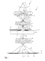
- FIG. 1 is a schematic illustration of a transmission electron microscope.
- the transmission electron microscope 1 comprises an illumination system 2 including an electron beam source 3 emitting an electron beam 5.
- the electron beam 5 is focused in a sample plane 9 by an electron lens 7 of the illumination system 2.
- electrons are incident on a location within the sample plane 9 from various directions. Trajectories of these electrons and their directions are located within a cone defined by an outer cone angle ⁇ 0 .
- the outer cone angle ⁇ 0 typically has values from within a range from 8 mrad to 15 mrad, and a diameter of the beam focus in the sample plane 9 may typically amount, in such illumination systems, to 0.2 nm to 100 nm.
- the illumination system 2 may, however, also include a corrector schematically indicated at 11 in Figure 1 .
- the outer cone angle ⁇ 0 may typically amount to 20 mrad to 50 mrad, and a diameter of the beam focus in the sample plane 9 can be from within a range from below 0.1 nm to 100 nm.
- a beam deflector (not shown in Figure 1 ) can be disposed in this beam path in order to displace the location of incidence of the electron beam in the sample plane 9 or to scan the location of incidence across a region within the sample plane 9.
- An objective lens 13 is disposed in the beam path downstream of the sample plane 9 such that an object plane of the objective lens 13 coincides with the sample plane 9.
- the objective lens 13 has a diffraction plane 15 corresponding to the object plane such that electrons traversing the object plane 9 at different angles relative to an optical axis 17 of the electron microscope 1 traverse the diffraction plane 15 at different locations. Moreover, electrons traversing the object plane at different locations but under same angles relative to the optical axis traverse the diffraction plane at a same location.
- the objective lens 13 images the object plane 9 into an intermediate image plane 19.
- a first projection system 21 is disposed in the beam path downstream of the objective lens 13.
- the first projection system 21 images the intermediate image plane 19 into a second intermediate image plane 23, and the first projection system 21 generates an image of the diffraction plane 15 in a plane 25.
- the first projection system 21 comprises three electron optical lenses which can be independently energized by a controller (not shown in Figure 1 ) of the transmission electron microscopy system 1 in order to change a magnification of the imaging of the diffraction plane 15 into the intermediate diffraction plane 25 without changing a position of the intermediate diffraction plane 25 along the optical axis 17.
- An aperture 27 is disposed in the intermediate diffraction plane 25.
- the aperture 27 comprises a circular opening defined by an outer edge 29 of the opening, which is also an inner edge of the aperture plate, wherein the outer edge 29 extends along a circle having a radius r 1 and its center on the optical axis 17.
- FIG. 1 An outer bounding surface of a beam of electrons having traversed the sample plane without scattering, i.e. of the beam of bright field electrons, is indicated with reference numeral 31 in Figure 1 . Electrons having experienced a significant amount of scattering in the sample plane are referred to as dark field electrons. These dark field electrons are shown in Figure 1 as a hollow cone having a circular ring-shaped beam cross section and having an inner bounding surface indicated at reference numeral 33 and an outer bounding surface indicated at reference numeral 35.
- the radius r 1 and the magnification of the first projection system 21 are adjusted such that at least the dark field electrons may not traverse the aperture 27 and such that at least a portion of the bright field electrons may traverse the aperture 27.
- a dark field detector 37 can be disposed in the beam path upstream of the aperture 27 in order to detect dark field electrons.
- the dark field detector 37 may comprise a ring-shaped active electron sensitive surface.
- the dark field detector 37 includes a central opening 40 which can be traversed by the bright field electrons. Due to manufacturing limitations, the active electron sensitive surface of the detector 37 does not extend, in the radially inwards direction, exactly towards the edge of the opening 40, such that the inner limiting angle 33 of detectable dark field electrons is defined by the inner edge of the active electron sensitive surface of the detector 37 rather than the diameter of the opening 40.
- magnification of the first projection system 21 and the radius r 1 of the opening of the aperture 27 are selected such that those bright field electrons which traverse the sample plane 9 at an angle ⁇ 0 relative to the optical axis may just traverse the aperture 27. It is, however, also possible to increase the magnification of the projection system 21 or to reduce the radius r 1 such that only those bright field electrons may traverse the aperture 27 which traverse the sample plane at an angle relative to the optical axis which is smaller than a maximum angle which, in turn, is smaller than the outer cone angle ⁇ 0 .
- a second projection system 41 is disposed in the beam path downstream of the intermediate diffraction plane 25.
- the second projection system 41 images the first intermediate diffraction plane 25 into a second intermediate diffraction plane 43.
- a bright field detector 45 is disposed in the second intermediate diffraction plane 43.
- the bright field detector 45 is configured such that it can only detect those bright field electrons 39 which traverse the sample plane 9 at an angle relative to the optical axis which is greater than a minimum angle, such that the bright field electrons detectable by the bright field detector 45 form a beam of a hollow cone shape and having a circular ring-shaped beam cross section, wherein an inner bounding surface of this beam upstream of the bright field detector 45 is indicated with reference numeral 47 in Figure 1 .
- the bright field detector 45 is disposed in the second intermediate diffraction plane 43, and the bright field detector 45 can be located in the beam path downstream of the second intermediate diffraction plane 43 where the aperture 51.
- the bright field detector 45 may comprise a ring-shaped active electron sensitive surface.
- the inner radius of the electron sensitive surface determines a minimum amount of scattering which the electrons must experience in the sample in order to be detected by the bright field detector 45.
- the outer radius of the ring-shaped electron sensitive surface determines a maximum amount of scattering which the electrons may experience within the sample in order to be detected by the bright field detector 45.
- a magnification of the second projection system 41 can be changed without changing a position of the second intermediate diffraction plane 43 along the optical axis 17.
- the second projection system 41 may comprise three or more electron optical lenses which can be independently energized by the controller of the transmission electron microscopy system 1.
- a minimum angle relative to the optical axis 17 at which bright field electrons detectable by the bright field detector 45 may traverse the sample plane 9 can be selected by adjusting the magnification of the second projection system 41 and the radius r 2 of the inner edge of the bright field detector 45 and of the outer edge of the aperture 51, respectively.
- plural apertures 51 having different radii r 2 can be provided, wherein one of the plural apertures is selectively disposed upstream of the bright field detector 45 in order to select a desired radius r 2 .
- the transmission electron microscopy system 1 allows to adjust the maximum angle relative to the optical axis of bright field electrons traversing the sample plane by adjusting the magnification of the first projection system 21 and/or the radius r 1 .
- an outer bounding surface 39 of the detected bright field electron beam can be adjusted by selecting the magnification of the first projection system 21 and or/the radius r 1 .
- the minimum angle relative to the optical axis of detected bright field electrons traversing the sample can be adjusted by adjusting the magnification of the second projection system 41 and/or by adjusting the radius r 2 .
- the inner bounding surface 47 of the detected bright field electron beam can be adjusted by selecting the magnification of the second projection system 41 and/or the radius r 2 .
- An energy filter 61 can be disposed in the beam path between the first intermediate diffraction plane 25 and the second intermediate diffraction plane 43 in order to provide energy resolved detection of bright field electrons.
- an aperture 65 having a slit-shaped opening is disposed in a spectral plane 63 of the energy filter 61, wherein only bright field electrons having kinetic energies from within a narrow energy range may traverse the slit-shaped opening of the aperture 65.
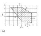
- Figure 2 is a schematic illustration of angular ranges of bright field electrons which can be detected with the transmission electron microscopy system shown in Figure 1 according to an exemplary embodiment.
- the opening 29 of the aperture 27 has a radius r 1 of 300 ⁇ m
- the magnification of the first projection system 21 is set to a value of 8
- the detector 45 has a ring-shaped detection surface having an inner radius r 2 and an outer radius such that it detects electrons traversing the sample at angles from 51 mrad (corresponding to line 47 in Figure 1 ) to 220 mrad (corresponding to line 39 in Figure 1 ).
- Figure 2 shows the angles, in mrad, in the sample plane of trajectories of detectable electrons in dependence of the magnification M(PII) of the second projection system 41, wherein the detectable electrons are indicated by a hatched region defined by lines 101, 102, 103, 104 and 105.
- the maximum angle relative to the optical axis amounts to about 22 mrad in the illustrated example.
- the minimum angle of the detectable bright field electrons is defined by the inner edge of the ring-shaped detector having the radius r 2 . While this radius is constant, the angles at which the bright field electrons traversing the sample are incident on the inner edge of the detector 45 increase with decreasing magnification M(PII) corresponding to line 101 in Figure 2 .
- the maximum angle of detectable bright field electrons is determined by the outer radius of the detector 45.
- the angle of bright field electrons traversing the sample and incident on the outer edge of the detector 45 decreases with increasing magnification of the second projection system 41 according to line 104 in Figure 2 .
- the inner angle 47 of the detectable bright field electrons changes as shown by line 102 in Figure 2 .
- the line 103 in Figure 2 represents the maximum magnification M(PII) of the illustrated exemplary transmission microscopy system.
- M(PII) which are smaller than the magnification at the intersection of lines 101 and 105, the magnification of the second projection system 41 is so small that all bright field electrons traverse the plane 43 of the detector 45 within the circle having the radius r 2 such that they are not detectable.
- angular ranges of detectable bright field electrons can be achieved, for example, by changing the radius r 1 of the opening 29 of the aperture 27, for example, the radius r 1 can be changed to have values of 200 ⁇ m or 400 ⁇ m. Also, the magnification of the first projection system 21 can be changed, for example such that the magnification is five times or sixteen times.
- FIG 3 is a schematic illustration of a further embodiment of a transmission electron microscopy system.
- the transmission electron microscopy system shown in Figure 3 has a configuration similar to the system illustrated with reference to Figure 1 .
- the system shown in Figure 3 differs from the system illustrated with reference to Figure 1 mainly in the manner how the minimum angle and the maximum angle relative to the optical axis of bright field electrons traversing the sample plane 9 and detected by a bright field detector 45 are adjusted.
- the minimum angle of these bright field electrons and, accordingly, an inner bounding surface 47 of the detected bright field electron beam is defined by an aperture 71 located in a first intermediate diffraction plane 25.
- the intermediate diffraction plane 25 is an image of a diffraction plane 15 of an objective lens 13 of the transmission electron microscopy system 1, wherein the image is generated by a first projection system 21.
- the aperture 71 has a circular shape and an outer edge 73 extending about an optical axis 17 of the microscopy system 1 along a circle having a radius r 3 .
- the aperture 71 absorbs bright field electrons traversing the sample plane 9 at angles which are smaller than a minimum angle. The minimum angle can be adjusted by changing the magnification of the first projection system 21 and or by changing the radius r 3 of the aperture 71.
- the aperture 71 disposed in the first intermediate diffraction plane 25 has a central region, centered relative to the optical axis, which does not allow electrons to traverse the aperture. Outside of the central region, the electrons may traverse the aperture, however.
- the aperture 71 may include a ring-shaped opening having a central portion, centered relative to the optical axis, which does not allow electrons to traverse, a ring-shaped portion surrounding this central portion which allows electrons to traverse, and a peripheral portion surrounding the ring-shaped portion which does not allow electrons to traverse the aperture.
- the magnification of the first projection system can be adjusted in dependence of the set outer cone angle ⁇ 0 of the illumination system and in dependence of the outer radius of the ring-shaped region allowing electrons to traverse such that dark field electrons may not traverse the aperture since they are incident on the peripheral portion which does not allow electrons to traverse.
- the maximum angle of bright field electrons traversing the sample plane 9 and detectable by the bright field detector 45 is defined by an outer edge 75 of the bright field detector 45, wherein the outer edge 75 extends about the optical axis 17 along a circle having a radius r 4 .
- the bright field detector 45 may have a greater extension in the second diffraction plane 43 if the bright field detector 45 is disposed downstream of an aperture disposed in the second diffraction plane 43 and having a circular opening extending about the optical axis 17 along a circle having the radius r 4 .
- the second intermediate diffraction plane 43 is generated by imaging the first intermediate diffraction plane 25 using a second projection system 41.
- the radius r 4 defines the maximum angle of detected bright field electrons traversing the sample plane 9. This maximum angle can be adjusted by changing the radius r 4 and/or by changing the magnification of the second projection system 41.
- the transmission electron microscopy system illustrated with reference to Figures 1 and 3 above are operated in a scanning mode of operation (scanning transmission electron microscope, STEM).
- a scanning mode of operation a focused illumination beam is scanned across the sample plane, and electrons having traversed with the sample are detected. It is not necessary that the detection itself is position dependent since position information relating to the sample can be derived from the actual scanned positions of the illumination beam.
- the illustrated transmission electron microscopes can be, however, also operated according to the normal TEM mode, in which an extended region of the object is simultaneously illuminated with electrons and wherein the extended region is imaged, using the first and second projection systems 21, 41 onto a position resolving detector, such as a CCD camera sensitive to electrons.
- the dark field detector 37 and the aperture 27 can remain in place since the openings of the dark field detector and the aperture 27 are sufficiently large such that they do not limit the image size.
- one or more of the apertures 71, the dark field detector 37 and the ring-shaped detector 45 of the system shown in Figure 3 can be mounted on manipulators in order to remove those components from the beam path.
Landscapes
- Chemical & Material Sciences (AREA)
- Analytical Chemistry (AREA)
- Analysing Materials By The Use Of Radiation (AREA)
- Electron Sources, Ion Sources (AREA)
Applications Claiming Priority (1)
| Application Number | Priority Date | Filing Date | Title |
|---|---|---|---|
| DE201210007868 DE102012007868A1 (de) | 2012-04-19 | 2012-04-19 | Transmissionselektronenmikroskopiesystem |
Publications (2)
| Publication Number | Publication Date |
|---|---|
| EP2654067A2 true EP2654067A2 (de) | 2013-10-23 |
| EP2654067A3 EP2654067A3 (de) | 2015-01-07 |
Family
ID=48141727
Family Applications (1)
| Application Number | Title | Priority Date | Filing Date |
|---|---|---|---|
| EP20130002044 Withdrawn EP2654067A3 (de) | 2012-04-19 | 2013-04-18 | Transmissionselektronenmikroskop und -verfahren zum Betrieb eines Transmissionselektronenmikroskops |
Country Status (3)
| Country | Link |
|---|---|
| US (1) | US8748819B2 (de) |
| EP (1) | EP2654067A3 (de) |
| DE (1) | DE102012007868A1 (de) |
Families Citing this family (6)
| Publication number | Priority date | Publication date | Assignee | Title |
|---|---|---|---|---|
| DE102012007868A1 (de) * | 2012-04-19 | 2013-10-24 | Carl Zeiss Microscopy Gmbh | Transmissionselektronenmikroskopiesystem |
| DE102013019855A1 (de) | 2013-11-25 | 2015-05-28 | Carl Zeiss Microscopy Gmbh | Elektronenmikroskop |
| JP6702807B2 (ja) * | 2016-06-14 | 2020-06-03 | 日本電子株式会社 | 電子顕微鏡および画像取得方法 |
| CN107796837B (zh) * | 2017-10-09 | 2019-10-29 | 南京大学 | 一种成像装置、成像方法及成像系统 |
| JP7193694B2 (ja) * | 2018-07-26 | 2022-12-21 | 国立研究開発法人理化学研究所 | 電子顕微鏡およびそれを用いた試料観察方法 |
| JP7693426B2 (ja) * | 2021-07-12 | 2025-06-17 | キオクシア株式会社 | 解析方法 |
Family Cites Families (21)
| Publication number | Priority date | Publication date | Assignee | Title |
|---|---|---|---|---|
| US3857034A (en) | 1970-08-31 | 1974-12-24 | Max Planck Gesellschaft | Scanning charged beam particle beam microscope |
| DE2043749C3 (de) * | 1970-08-31 | 1975-08-21 | Max-Planck-Gesellschaft Zur Foerderung Der Wissenschaften E.V., 3400 Goettingen | Raster-Korpuskularstrahlmikroskop |
| US5866905A (en) * | 1991-05-15 | 1999-02-02 | Hitachi, Ltd. | Electron microscope |
| JP3422045B2 (ja) * | 1993-06-21 | 2003-06-30 | 株式会社日立製作所 | 組成及び格子歪測定用電子顕微鏡及びその観察方法 |
| DE19855629A1 (de) * | 1998-12-02 | 2000-06-08 | Leo Elektronenmikroskopie Gmbh | Teilchenoptische Anordnung und Verfahren zur teilchenoptischen Erzeugung von Mikrostrukturen |
| JPH11250850A (ja) * | 1998-03-02 | 1999-09-17 | Hitachi Ltd | 走査電子顕微鏡及び顕微方法並びに対話型入力装置 |
| JP3888980B2 (ja) * | 2003-03-18 | 2007-03-07 | 株式会社日立ハイテクノロジーズ | 物質同定システム |
| JP4563733B2 (ja) | 2004-06-25 | 2010-10-13 | 株式会社日立ハイテクノロジーズ | 走査透過電子顕微鏡及びそれを用いた電子線エネルギー分光方法 |
| JP2006196236A (ja) * | 2005-01-12 | 2006-07-27 | Hitachi High-Technologies Corp | 電子顕微鏡及び観察方法 |
| JP4997013B2 (ja) * | 2007-07-31 | 2012-08-08 | 株式会社日立ハイテクノロジーズ | 電子分光器を備えた電子顕微鏡 |
| DE102009016861A1 (de) * | 2009-04-08 | 2010-10-21 | Carl Zeiss Nts Gmbh | Teilchenstrahlmikroskop |
| JP5390926B2 (ja) * | 2009-04-28 | 2014-01-15 | 日本電子株式会社 | 環状明視野像観察装置 |
| JP5405937B2 (ja) * | 2009-08-07 | 2014-02-05 | 株式会社日立製作所 | 透過型電子顕微鏡およびそれを用いた試料像の観察方法 |
| EP2534667A2 (de) * | 2010-02-10 | 2012-12-19 | Mochii, Inc. (d/b/a Voxa) | Dunkelfeld-elektronenmikroskopie mit aberrationskorrektur |
| US8598526B2 (en) * | 2010-03-01 | 2013-12-03 | Carl Zeiss Microscopy Gmbh | Transmission electron microscope |
| WO2011156421A2 (en) * | 2010-06-07 | 2011-12-15 | Christopher Su-Yan Own | Incoherent transmission electron microscopy |
| WO2012009543A2 (en) * | 2010-07-14 | 2012-01-19 | Fei Company | Improved contrast for scanning confocal electron microscope |
| EP2413345B1 (de) * | 2010-07-29 | 2013-02-20 | Carl Zeiss NTS GmbH | Strahlensystem mit geladenen Teilchen |
| JP5799653B2 (ja) * | 2011-08-17 | 2015-10-28 | 富士通株式会社 | 画像処理装置、像を生成する方法並びにシステム |
| JP5934513B2 (ja) * | 2012-02-09 | 2016-06-15 | 日本電子株式会社 | 透過電子顕微鏡 |
| DE102012007868A1 (de) * | 2012-04-19 | 2013-10-24 | Carl Zeiss Microscopy Gmbh | Transmissionselektronenmikroskopiesystem |
-
2012
- 2012-04-19 DE DE201210007868 patent/DE102012007868A1/de not_active Withdrawn
-
2013
- 2013-04-17 US US13/864,600 patent/US8748819B2/en not_active Expired - Fee Related
- 2013-04-18 EP EP20130002044 patent/EP2654067A3/de not_active Withdrawn
Non-Patent Citations (1)
| Title |
|---|
| None |
Also Published As
| Publication number | Publication date |
|---|---|
| US8748819B2 (en) | 2014-06-10 |
| US20130292566A1 (en) | 2013-11-07 |
| DE102012007868A1 (de) | 2013-10-24 |
| EP2654067A3 (de) | 2015-01-07 |
Similar Documents
| Publication | Publication Date | Title |
|---|---|---|
| US8748819B2 (en) | Transmission electron microscopy system and method of operating a transmission electron microscopy system | |
| EP2912442B1 (de) | Vorrichtung und verfahren zur inspektion einer probenoberfläche | |
| US20220246388A1 (en) | Multiple particle beam microscope and associated method with an improved focus setting taking into account an image plane tilt | |
| JP5871440B2 (ja) | 走査共焦点電子顕微鏡のコントラストの向上 | |
| EP2864997B1 (de) | Vorrichtung und verfahren zur inspektion einer probenoberfläche | |
| US8471203B2 (en) | Particle-beam microscope | |
| US8598526B2 (en) | Transmission electron microscope | |
| JP6278553B2 (ja) | 2次電子光学系及び検出デバイス | |
| WO2014188882A1 (ja) | 荷電粒子線応用装置 | |
| TWI613693B (zh) | 用於成像訊號帶電粒子束的系統、用於成像訊號帶電粒子束的方法及帶電粒子束裝置 | |
| JP7523742B2 (ja) | コントラスト補正レンズ系を備えた複数粒子ビームシステム | |
| EP2378537B1 (de) | Verfahren zum Betreiben einer Teilchenstrahlvorrichtung | |
| CN113466266B (zh) | 用于获取3d衍射数据的方法和系统 | |
| CN113125478B (zh) | 用于晶带轴自动对准的方法和系统 | |
| JP5934513B2 (ja) | 透過電子顕微鏡 | |
| EP2600379B1 (de) | Transmissions-rasterelektronenmikroskop und achseneinstellungsverfahren dafür | |
| WO2025004191A1 (ja) | 荷電粒子線装置 | |
| JP6962979B2 (ja) | 暗視野像の取得方法 | |
| JP2022155554A (ja) | 三次元電子回折データを取得するための方法およびシステム | |
| US20020074939A1 (en) | Charged particle beam apparatus | |
| JP2018106947A (ja) | 電子線検査装置 |
Legal Events
| Date | Code | Title | Description |
|---|---|---|---|
| PUAI | Public reference made under article 153(3) epc to a published international application that has entered the european phase |
Free format text: ORIGINAL CODE: 0009012 |
|
| AK | Designated contracting states |
Kind code of ref document: A2 Designated state(s): AL AT BE BG CH CY CZ DE DK EE ES FI FR GB GR HR HU IE IS IT LI LT LU LV MC MK MT NL NO PL PT RO RS SE SI SK SM TR |
|
| AX | Request for extension of the european patent |
Extension state: BA ME |
|
| PUAL | Search report despatched |
Free format text: ORIGINAL CODE: 0009013 |
|
| AK | Designated contracting states |
Kind code of ref document: A3 Designated state(s): AL AT BE BG CH CY CZ DE DK EE ES FI FR GB GR HR HU IE IS IT LI LT LU LV MC MK MT NL NO PL PT RO RS SE SI SK SM TR |
|
| AX | Request for extension of the european patent |
Extension state: BA ME |
|
| RIC1 | Information provided on ipc code assigned before grant |
Ipc: H01J 37/04 20060101AFI20141201BHEP Ipc: H01J 37/26 20060101ALI20141201BHEP |
|
| 17P | Request for examination filed |
Effective date: 20150707 |
|
| RBV | Designated contracting states (corrected) |
Designated state(s): AL AT BE BG CH CY CZ DE DK EE ES FI FR GB GR HR HU IE IS IT LI LT LU LV MC MK MT NL NO PL PT RO RS SE SI SK SM TR |
|
| 17Q | First examination report despatched |
Effective date: 20160406 |
|
| 18W | Application withdrawn |
Effective date: 20170427 |
|
| STAA | Information on the status of an ep patent application or granted ep patent |
Free format text: STATUS: THE APPLICATION HAS BEEN WITHDRAWN |