EP2652867B1 - Mehrstufiger spannungswandler - Google Patents
Mehrstufiger spannungswandler Download PDFInfo
- Publication number
- EP2652867B1 EP2652867B1 EP10860858.9A EP10860858A EP2652867B1 EP 2652867 B1 EP2652867 B1 EP 2652867B1 EP 10860858 A EP10860858 A EP 10860858A EP 2652867 B1 EP2652867 B1 EP 2652867B1
- Authority
- EP
- European Patent Office
- Prior art keywords
- power semiconductor
- power
- energy store
- output terminal
- switching
- Prior art date
- Legal status (The legal status is an assumption and is not a legal conclusion. Google has not performed a legal analysis and makes no representation as to the accuracy of the status listed.)
- Active
Links
Images




Classifications
-
- G—PHYSICS
- G05—CONTROLLING; REGULATING
- G05F—SYSTEMS FOR REGULATING ELECTRIC OR MAGNETIC VARIABLES
- G05F3/00—Non-retroactive systems for regulating electric variables by using an uncontrolled element, or an uncontrolled combination of elements, such element or such combination having self-regulating properties
- G05F3/02—Regulating voltage or current
- G05F3/08—Regulating voltage or current wherein the variable is DC
-
- H—ELECTRICITY
- H02—GENERATION; CONVERSION OR DISTRIBUTION OF ELECTRIC POWER
- H02M—APPARATUS FOR CONVERSION BETWEEN AC AND AC, BETWEEN AC AND DC, OR BETWEEN DC AND DC, AND FOR USE WITH MAINS OR SIMILAR POWER SUPPLY SYSTEMS; CONVERSION OF DC OR AC INPUT POWER INTO SURGE OUTPUT POWER; CONTROL OR REGULATION THEREOF
- H02M7/00—Conversion of AC power input into DC power output; Conversion of DC power input into AC power output
- H02M7/42—Conversion of DC power input into AC power output without possibility of reversal
- H02M7/44—Conversion of DC power input into AC power output without possibility of reversal by static converters
- H02M7/48—Conversion of DC power input into AC power output without possibility of reversal by static converters using discharge tubes with control electrode or semiconductor devices with control electrode
- H02M7/483—Converters with outputs that each can have more than two voltages levels
-
- H—ELECTRICITY
- H02—GENERATION; CONVERSION OR DISTRIBUTION OF ELECTRIC POWER
- H02M—APPARATUS FOR CONVERSION BETWEEN AC AND AC, BETWEEN AC AND DC, OR BETWEEN DC AND DC, AND FOR USE WITH MAINS OR SIMILAR POWER SUPPLY SYSTEMS; CONVERSION OF DC OR AC INPUT POWER INTO SURGE OUTPUT POWER; CONTROL OR REGULATION THEREOF
- H02M7/00—Conversion of AC power input into DC power output; Conversion of DC power input into AC power output
- H02M7/42—Conversion of DC power input into AC power output without possibility of reversal
- H02M7/44—Conversion of DC power input into AC power output without possibility of reversal by static converters
- H02M7/48—Conversion of DC power input into AC power output without possibility of reversal by static converters using discharge tubes with control electrode or semiconductor devices with control electrode
- H02M7/483—Converters with outputs that each can have more than two voltages levels
- H02M7/4837—Flying capacitor converters
-
- H—ELECTRICITY
- H02—GENERATION; CONVERSION OR DISTRIBUTION OF ELECTRIC POWER
- H02M—APPARATUS FOR CONVERSION BETWEEN AC AND AC, BETWEEN AC AND DC, OR BETWEEN DC AND DC, AND FOR USE WITH MAINS OR SIMILAR POWER SUPPLY SYSTEMS; CONVERSION OF DC OR AC INPUT POWER INTO SURGE OUTPUT POWER; CONTROL OR REGULATION THEREOF
- H02M1/00—Details of apparatus for conversion
- H02M1/0095—Hybrid converter topologies, e.g. NPC mixed with flying capacitor, thyristor converter mixed with MMC or charge pump mixed with buck
-
- H—ELECTRICITY
- H02—GENERATION; CONVERSION OR DISTRIBUTION OF ELECTRIC POWER
- H02M—APPARATUS FOR CONVERSION BETWEEN AC AND AC, BETWEEN AC AND DC, OR BETWEEN DC AND DC, AND FOR USE WITH MAINS OR SIMILAR POWER SUPPLY SYSTEMS; CONVERSION OF DC OR AC INPUT POWER INTO SURGE OUTPUT POWER; CONTROL OR REGULATION THEREOF
- H02M7/00—Conversion of AC power input into DC power output; Conversion of DC power input into AC power output
- H02M7/42—Conversion of DC power input into AC power output without possibility of reversal
- H02M7/44—Conversion of DC power input into AC power output without possibility of reversal by static converters
- H02M7/48—Conversion of DC power input into AC power output without possibility of reversal by static converters using discharge tubes with control electrode or semiconductor devices with control electrode
- H02M7/483—Converters with outputs that each can have more than two voltages levels
- H02M7/487—Neutral point clamped inverters
Definitions
- the invention relates to the field of voltage source converter, and more particularly to multi-level voltage source converter (VSC).
- VSC multi-level voltage source converter
- multi-level voltage source converter is widely used, which can equivalently decrease the switching frequency and improve the output waveform quality.
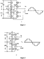
- Figure 1 illustrates a topology according to a conventional multi-level voltage converter, wherein a switching gear cell 1 includes a first energy store 100 and a second energy store 101 connected in series with power semiconductors for switching, for example, five voltage levels.
- a first, second, third and fourth power semiconductors 110, 111, 112, 113 are connected in series, a fifth and sixth power semiconductors 114, 115 are connected in series.
- the first and fourth power semiconductors 110, 114 are respectively connected with the first and second energy stores 100, 101, and the junction point A between the first and second energy stores 100, 101, the junction point B between the fifth and sixth power semiconductors 114, 115, and the junction point C between the second and third power semiconductors 111,112 are connected with each other.
- the switching gear cell further includes a seventh, eighth, ninth and tenth power semiconductors 116, 117, 118, 119 are connected in series, a eleventh and twelfth power semiconductors 120, 121 are connected in series.
- the seventh and tenth power semiconductors 116, 119 are respectively connected with the first and second energy stores 100, 101, and the junction point A between the first and second energy stores 100, 101, the junction point D between the eleventh and twelfth power semiconductors 120, 121 are connected with each other.
- the junction point between the eighth and ninth power semiconductors 117,118 is arranged for output terminal for outputting the multi-level voltage, for example, a five -level voltage as shown at the right side of figure 1 .
- Each of the first, second, third, fourth, seventh, eighth, ninth and tenth power semiconductors 110, 111, 112, 113, 116, 117, 118, 119 is a drivable unidirectional power semiconductor switch with an anti-paralleled uncontrolled unidirectional current-carrying semiconductor , such as IGCT or IGBT etc, and each of the fifth, sixth, eleventh, and twelfth power semiconductors is a uncontrolled unidirectional current-carrying direction power semiconductor, such as power diode.
- Figure 2 illustrates a topology according to another conventional multi-level voltage converter.
- a switching gear cell 2 uses cascaded H-bridges.
- the first H-bridge of the switching gear cell 2 includes a first energy store 200, a first and second power semiconductors 210, 211 connected in series, a third and fourth power semiconductors 212, 213 connected in series. And, the first energy store 200, the first power semiconductor 210 and the third power semiconductor 212 are connected with each other at junction point A, the first energy store 200, the second power semiconductor 211 and the fourth power semiconductor 213 are connected with each other at junction point B.
- the second bridge of the switching gear cell 2 has a similar topology as to the first H-bridge, which includes a second energy store 201, a fifth, sixth, seventh, and eighth power semiconductors 214, 215, 216, 217.
- the junction point between the first and second power semiconductors 210, 211 and the junction point between the fifth and sixth power semiconductors 214, 215 are connected with each other.
- the voltage is output between the junction point between the third and fourth power semiconductors and the junction point between the seventh and eighth power semiconductors.
- the output voltage waveform is shown at the right side of figure 2 .
- Each of the first, second, third, fourth, fifth, sixth, seventh, eighth power semiconductors is a drivable unidirectional power semiconductor switch with an anti-paralleled uncontrolled unidirectional current-carrying semiconductor .
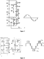
- Figure 3 illustrates a topology according to another conventional multi-level voltage converter.
- a switching gear cell 3 includes a first energy store 300 and a second energy store 301 connected in series with power semiconductors for switching, for example, five voltage levels.
- a first, second, third and fourth power semiconductors 410, 411, 412, 413 are connected in series, a fifth and sixth power semiconductors 414, 415 are connected in series.
- the first and fourth power semiconductors 410, 413 are respectively connected with the first and second energy stores 400, 401, and the junction point A between the first and second energy stores 400, 401, the junction point B between the fifth and sixth power semiconductors 414, 415 are connected with each other.
- the switching gear cell further includes a third energy store 402, a seventh and eighth power semiconductors 416, 417 connected in series, and a ninth and tenth power semiconductors 418, 419 connected in series.
- One end of the third energy store 402, the seventh and ninth power semiconductors 416, 418 are connected with each other, and the other end of the third energy store 402, the eighth and tenth power semiconductors 417, 419 are connected with each other.
- the junction point between the second and third second and third power semiconductors 411, 412 is connected with the junction point between the ninth and tenth power semiconductors 418, 419.
- the voltage is output at the junction point between the seventh and eighth power semiconductors 416, 417.
- Each of the first, second, third, fourth, seventh, eighth, ninth and tenth power semiconductors is a drivable unidirectional power semiconductor switch with an anti-paralleled uncontrolled unidirectional current-carrying semiconductor
- each of the fifth and sixth power semiconductors is a uncontrolled unidirectional current-carrying direction power semiconductor. Its output waveform is shown at the right side of figure 3 .
- a switchgear has a first energy store and a second energy store connected in series, a first, second, third and fourth power semiconductor switch connected in series.
- the first and fourth power semiconductor are respectively connected to the first energy store and the second energy store.
- a third energy store is connected to the junction between the first and the second power semiconductor and the junction between the third and the fourth semiconductor.
- it includes a switching element connected directly to the junction pint between the second and the third power semiconductor and directly to the junction point between the first energy store and the second energy store.
- US 7, 639, 515 has at least drawbacks as that: 1. Due to a lower ration between the Vout and Vdc, it requires a higher voltage class of the power semiconductors, the power capacitor, and all the components of the converter related to the DC link. Higher voltage class of power semiconductor, power capacitor and all the related components leads to higher cost of voltage converter. 2. It requires a relatively large number of power semiconductors, which increases also the cost of the multi-level voltage converter but decreases the reliability.
- WO 2007/051321 A2 discloses a voltage charge circuit having a switching group formed by semiconductor switches that are connected with each other. Another switching group and a third switching group are connected to the group.
- WO 2007/051321 A2 discloses a converter circuit for switching a plurality of switching voltage levels.
- the converter circuit has a first switching group provided for each phase, the first switching group being formed by a first and a second controllable bidirectional power semiconductor switch that are interconnected.
- EP 2 110 939 A1 discloses a multiphase inverter for providing phase voltages at a plurality of phase outputs, comprising: at least three voltage inputs for receiving three different input voltage potentials; several, each with a phase output, associated switch assemblies, wherein in at least one of the switch assemblies current paths from the voltage inputs to one of the each switch assembly associated phase output are switchable to provide more than two output voltage levels there.
- a voltage source converter comprises: a multi-level voltage source converter, being adapted to output a multiple levels of a first voltage at one of two first output terminals through a multiple of first conducting paths; a first energy store; and a first switching element, being arranged to directly connected with the first output terminal, and being adapted to switch the first energy store in or out of the first conducting path so as to combine a level of the voltage of the first energy store with the level of the first voltage as a second voltage output at a second output terminal.
- the multi-level voltage source converter comprises: a second energy store; a third energy store, being arranged to be connected with the second energy store in series.
- the multi-level voltage source converter further comprises: a first, a second, a third and a fourth power semiconductors, being arranged to be connected in series, wherein the first power semiconductor is arranged to be connected to the second energy store, the fourth power semiconductor is arranged to be connected to the third energy store, the junction point between the second and the third energy stores is connected to the junction point between the second and the third power semiconductors; a fifth power semiconductor, being arranged to be connected between the junction point between the first and second power semiconductors and one of the first output terminals and in series with the first power semiconductor; a sixth power semiconductor, being arranged to be connected between the junction point between the third and fourth power semiconductors and the other of the first output terminals and in series with the fourth power semiconductor; each of the first, second, third, fourth, fifth and sixth power semiconductors being a drivable unidirectional power semiconductor switch with an anti-paralleled uncontrolled unidirectional current-carrying semiconductor; or: a first and a second power semiconductors, being arranged to be connected in anti-serie
- the first switching element comprises a seventh and eighth semiconductors connected in series at the second output terminal, either of the seventh and eighth is a drivable unidirectional power semiconductor switch with an anti-paralleled uncontrolled unidirectional power semiconductor.
- the first energy store is arranged to be connected with the first switching element in parallel between the two first output terminals.
- the seventh and the eighth semiconductors are respectively connected to the fifth power semiconductor and the sixth power semiconductor at the two first output terminals of the multi-level voltage source converter in anti-series.
- the voltage class of each of the power semiconductors can be kept lower with the number of the power semiconductors unchanged. Besides, V DRM is lowed as compared to conventional topology. This renders the reduction of the cost and the increase of the liability.
- a voltage source converter comprises: a multi-level voltage source converter, being adapted to output a multiple levels of a first voltage at one of two first output terminals through a multiple of first conducting paths; a first energy store; and a first switching element, being arranged to directly connected with the first output terminal, and being adapted to switch the first energy store in or out of the first conducting path so as to combine a level of the voltage of the first energy store with the level of the first voltage as a second voltage output at a second output terminal.
- the multi-level voltage source converter comprises: a second energy store; a third energy store, being arranged to be connected with the second energy store in series.
- the multi-level voltage source converter further comprises either: a first, a second, a third and a fourth power semiconductors, being arranged to be connected in series, wherein the first power semiconductor is arranged to be connected to the second energy store, the fourth power semiconductor is arranged to be connected to the third energy store, the junction point between the second and the third energy stores is connected to the junction point between the second and the third power semiconductors; a fifth power semiconductor, being arranged to be connected between the junction point between the first and second power semiconductors and one of the first output terminals and in series with the first power semiconductor; a sixth power semiconductor, being arranged to be connected between the junction point between the third and fourth power semiconductors and the other of the first output terminals and in series with the fourth power semiconductor; each of the first, second, third, fourth, fifth and sixth power semiconductors being a drivable unidirectional power semiconductor switch with an anti-paralleled uncontrolled unidirectional current-carrying semiconductor; or: a first and a second power semiconductors, being arranged to be connected in anti-
- the first switching element comprises a seventh and eighth semiconductors connected in series at a first junction point, either of the seventh and eighth is a drivable unidirectional power semiconductor switch with an anti-paralleled uncontrolled unidirectional power semiconductor.
- the first switching element comprises a ninth and tenth power semiconductors, being arranged to be series-connected at a second junction point; a eleventh and twelfth power semiconductors, being arranged to be anti-series-connected at a third junction point.
- the eleventh power semiconductor is arranged to be connected with both of the first junction point and one of the first output terminals and the twelfth power semiconductor is arranged to be connected with both of the second junction point and the other of the first output terminals;
- the first energy store, the seventh and eighth power semiconductors, and the ninth and tenth power semiconductors are arranged to be connected in parallel.
- Each of the seventh, eighth, ninth, tenth, eleventh, and twelfth power semiconductors is a drivable unidirectional power semiconductor switch with an anti-paralleled uncontrolled unidirectional current-carrying semiconductor.
- a voltage source converter system comprises: a voltage source converter according to each of previous claims, being adapted to output a multiple levels of the second voltage at one of two second output terminals in a multiple of the first conducting paths; a fourth energy store; and a second switching element, being arranged to directly connected with the second output terminal, and being adapted to switch the fourth energy store in or out of the first conducting path so as to combine a level of the voltage of the fourth energy store with the level of the second voltage as a third voltage output at a third output terminal.
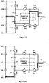
- a voltage source converter 4 comprises a multi-level voltage source converter 40, a first energy store 41, and a first switching element 42.
- the multi-level voltage source converter 40 can output a multiple levels of first voltage.
- the first voltage is arranged to be output at one of two first output terminals A and B through a multiple of first conducting paths P1. According to each switching state of the multi-level voltage source converter, one of the first conducting paths PI is selected with switching-on some of the power semiconductors used in it, which will be described in detail later.
- the first energy store 41 can store electrical energy, such as power capacitor.
- the first switching element 42 is directly connected with the first output terminals A and B, and it can switch the first energy store 41 in or out of the first conducting path PI so as to combine a level of the voltage of the first energy store with the level of the first voltage as a second voltage output at a second output terminal C.
- the voltage level of the first energy store is V dc
- the voltage level of the first voltage is V dc , 0, or - V dc
- the second voltage output is 2V dc, V dc , 0, or - V dc , or - 2V dc , which is a five-level output.
- the multi-level voltage source converter 40 comprises a second energy store 400, a third energy store 401.
- the second energy store 400 and the third energy store 401 are connected in series at junction point D. They can be of power capacitor and hold voltages with the same or different level. For example, the voltage level across either of the energy stores can be V dc .
- the multi-level voltage source converter 40 also includes a first, a second, a third and a fourth power semiconductors 402, 403, 404, 405, which are connected in series.
- the first power semiconductor 402 is connected to the second energy store 400 at a point opposite to the junction point D
- the fourth power semiconductor 405 is connected to the third energy store 401 at a point opposite to the junction point D.
- the junction point D between the second and the third energy stores 400, 401 is connected to the junction point E between the second and the third power semiconductors 403, 404.
- the multi-level voltage source converter 40 also comprises a fifth power semiconductor 406 and a sixth power semiconductor 407.
- the fifth power semiconductor 406 is connected between the junction point F between the first and second power semiconductors 402, 403 and one of the first output terminals A and in series with the first power semiconductor
- the sixth power semiconductor 407 is connected between the junction point G between the third and fourth power semiconductors 404, 405 and the other of the first output terminals B and in series with the fourth power semiconductor.
- Each of the first, second, third, fourth, fifth and sixth power semiconductors is a drivable unidirectional power semiconductor switch with an anti-paralleled uncontrolled unidirectional current-carrying semiconductor, such as IGCT or IGBT etc.
- the first conducting path PI can lead through:
- the multi-level voltage source converter 40 can output three-level voltage independent of the configuration and the switching states of the converter cascaded down with it. Besides, the number of power semiconductor is lower. Furthermore, the repetitive peak off-state voltage of each of the power semiconductors is reduced.
- Figure 5 illustrates an alternative topology to the embodiment of figure 4 .
- the difference therebetween is that the second and third power semiconductors 403, 404 are replaced by uncontrolled unidirectional current-carrying direction power semiconductors, such as power diode.
- the second power semiconductor 403 is connected with the first power semiconductor 402 in anti-series
- the third power semiconductor 404 is connected with the fourth power semiconductor 405 in anti-series.
- the first switching element 42 comprises a seventh and eighth semiconductors 420, 421 connected in series at junction point C.
- the seventh power semiconductor 420 is connected to the fifth power semiconductor 406 at junction point A in anti-series
- the eighth power semiconductor 421 is connected to the sixth power semiconductor 407 at junction point B in anti-series. Therefore, the first energy store 41 is connected with the first switching element in parallel between the two first output terminals A and B.
- Either of the seventh and eighth is a drivable unidirectional power semiconductor switch with an anti-paralleled uncontrolled unidirectional current-carrying semiconductor .
- the first conducting path can further lead through:
- Figures 5A to 5H illustrate the first conducting paths in each of the valid states according to the embodiments of figure 5 .
- the arrow in each of the figures indicates the conducting path P1.
- the first, fourth, fifth, sixth, seventh and eighth power semiconductors are referenced as V1, V2, V3, V4, V5 and V6, the second and third power semiconductors are referenced as D1, D2.
- Output voltage is the output at the second output terminal C, and for the purpose of specification, the voltage level of each of the first, second and third energy stores 41, 400, 401 is V dc with voltage polarity indicated in the figures.
- the row of "voltage" shows the voltage across each of the power semiconductors under each of the switching states.
- Table I Switching state V1 V2 V3 V4 V5 V6 Output voltage D1 D2 S1 1 0 1 0 0 1 2 ⁇ Vdc N/A N/A V DRM 0 Vdc/2 0 Vdc Vdc 0 Vdc Vdc/2
- the first conducting path PI is bidirectional. As shown in figure 5A , the first conducting path PI leads through the junction point between the second energy store and the first power semiconductor V1, the switching-on/free-wheeling first power semiconductor V1, the switching-on/free-wheeling fifth power semiconductor V3, and the first output terminal A; the first voltage level at the first output terminal A is V dc . Furthermore, from the first output terminal A, the first conducting path PI leads through the first energy store 41, the switching-on/free-wheeling eighth power semiconductor V6 and the second output terminal C. With respect to point NP, the voltage output at the second output terminal C is 2V dc .
- the first conducting path PI is unidirectional. As shown in figure 5B , the first conducting path PI leads through the junction point between the second energy store and the first power semiconductor V1, the switching-on first power semiconductor V1, the switching-on fifth power semiconductor V3, and the first output terminal A; the first voltage level at the first output terminal A is Vdc. Furthermore, from the first output terminal A, the first conducting path PI leads through the switching-on seventh power semiconductor V5 and and the second output terminal C. With respect to point NP, the voltage output at the second output terminal C is Vdc.
- Table III Switching state V1 V2 V3 V4 V5 V6 Output voltage D1 D2 S3 0 0 1 0 0 1 Vdc N/A N/A V DRM Vdc Vdc/2 0 Vdc Vdc 0 0 Vdc/2
- the first conducting path PI is unidirectional. As shown in figure 5B , the first conducting path PI leads through the junction point D between the second and third energy stores, the free-wheeling second power semiconductor, the switching-on fifth power semiconductor V3, and the first output terminal A; the first voltage level at the first output terminal A is 0. Furthermore, from the first output terminal A, the first conducting path PI leads through the first energy store 41, the switching-on eighth power semiconductor V6 and the second output terminal C. With respect to point NP, the voltage output at the second output terminal C is V dc .
- Table IV Switching state V1 V2 V3 V4 V5 V6 Output voltage D1 D2 S4 0 0 1 0 1 0 0 N/A N/A V DRM Vdc Vdc/2 0 Vdc 0 Vdc 0 Vdc/2
- the first conducting path PI is unidirectional. As shown in figure 5D , the first conducting path PI leads through the junction point D between the second and third energy stores, the free-wheeling second power semiconductor D1, the switching-on fifth power semiconductor V3, and the first output terminal A. Furthermore, from the first output terminal A, the first conducting path PI leads through the switching-on seventh power semiconductor V5 and the second output terminal C. With respect to point NP, the voltage output at the second output terminal C is 0.
- Table V Switching state V1 V2 V3 V4 V5 V6 Output voltage D1 D2 S5 0 0 0 1 0 1 0 N/A N/A V DRM Vdc/2 Vdc Vdc 0 Vdc 0 Vdc/2 0
- the first conducting path PI is unidirectional. As shown in figure 5E , the first conducting path PI leads through the junction point D between the second and third energy stores, the free-wheeling third power semiconductor D2, the switching-on sixth power semiconductor V4, and the first output terminal B; the first voltage level at the first output terminal B is the voltage level at junction point D (NP), for example 0. Furthermore, from the first output terminal B, the first conducting path PI leads through the free-wheeling eighth power semiconductor V6 and the second output terminal C. With respect to point NP, the voltage output at the second output terminal C is 0.
- the first conducting path PI is unidirectional. As shown in figure 5F , the first conducting path PI leads through the junction point D between the second and third energy stores, the free-wheeling third power semiconductor D2, the switching-on sixth power semiconductor V4, and the first output terminal B; the first voltage level at the first output terminal B is the voltage level at junction point D (NP), for example 0. Furthermore, from the first output terminal B, the first conducting path PI leads through the first energy store 41, the switching-on seventh power semiconductor V5 and the second output terminal C. With respect to point NP, the voltage output at the second output terminal C is -V dc .
- Table VII Switching state V1 V2 V3 V4 V5 V6 Output voltage D1 D2 S7 0 1 0 1 0 1 -Vdc N/A N/A V DRM Vdc/2 0 Vdc 0 Vdc 0 Vdc/2 Vdc
- the first conducting path PI is bidirectional. As shown in figure 5G , the first conducting path PI leads through the junction point between the third energy store 401 and the fourth power semiconductor V2, the switching-on/free-wheeling fourth power semiconductor V2, the switching-on/free-wheeling sixth power semiconductor V4, and the first output terminal B; the first voltage level at the first output terminal B is the voltage level at junction point D (NP), for example 0. Furthermore, from the first output terminal B, the first conducting path PI leads through the free-wheeling/switching-on eighth power semiconductor V6 and the second output terminal C. With respect to point NP, the voltage output at the second output terminal C is -V dc .
- Table VIII Switching state V1 V2 V3 V4 V5 V6 Output voltage D1 D2 S8 0 1 0 1 1 0 -2 ⁇ Vdc N/A N/A V DRM Vdc/2 0 Vdc 0 0 Vdc Vdc/2 Vdc
- the first conducting path PI is bidirectional. As shown in figure 5H , the first conducting path PI leads through the junction point between the third energy store 401 and the fourth power semiconductor V2, the switching-on/free-wheeling fourth power semiconductor V2, the switching-on/free-wheeling sixth power semiconductor V4, the first energy store, the switching-on seventh power semiconductor and the second output terminal B; the first voltage level at the first output terminal B is the voltage level at junction point D (NP), for example -V dc . Furthermore, from the first output terminal B, the first conducting path PI leads through the free-wheeling/switching-on seventh power semiconductor V5 and the second output terminal C. With respect to point NP, the voltage output at the second output terminal C is -2V dc .
- the voltage class of each of the power semiconductors can be kept lower with the number of the power semiconductors unchanged. Besides, V DRM is lowed as compared to conventional topology. This renders the reduction of the cost and the increase of the liability.
- the topology according to figure 4 is adapted to have some redundant switching states as below:
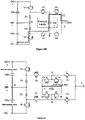
- Figure 6 illustrates a topology according to another embodiment of present invention.
- the topology differs from that of figure 4 in the switching element and the first energy store.
- the switching element 42 comprises a seventh and eighth power semiconductors 422, 423 series-connected at a first junction point, a ninth and tenth power semiconductors 424, 425 series-connected at a second junction point B, and a eleventh and twelfth power semiconductors 420, 421 anti-series-connected at a third junction point.
- the eleventh power semiconductor 420 is connected with both of the first junction point and one of the first output terminals A
- the twelfth power semiconductor 421 is connected with both of the second junction point and the other of the first output terminals B.
- the first energy store 41, the seventh and eighth power semiconductors 422, 423, and the ninth and tenth power semiconductors 424, 425 are arranged to be connected in parallel.
- Each of the seventh, eighth, ninth and eleventh, power semiconductors is a drivable unidirectional power semiconductor switch with an anti-paralleled uncontrolled unidirectional power semiconductor current-carrying semiconductor , such as IGCT or IGBT etc.
- Each of the tenth and twelfth power semiconductors is a drivable bidirectional power semiconductor switch.
- Switching states of the topology according to figure 6 is shown in Table IX.
- the first, fourth, fifth, sixth, seventh, eighth, ninth, tenth, eleventh and twelfth power semiconductors are referenced as V1, V6, V2, V7, V3, V4, V8, V9, V5, V10
- the second and third power semiconductors are referenced as D1, D2.
- Output voltage is the output at the second output terminal C, and for the purpose of specification, the voltage level of each of the first, second and third energy stores 41, 400, 401 is V dc with voltage polarity indicated in the figures.
- the row of "voltage" shows the voltage across each of the power semiconductors under each of the switching states.
- the first conducting path PI is bidirectional. As shown in figure 6 , the first conducting path P1 leads through the junction point between the second energy store and the first power semiconductor V1, the switching-on/free-wheeling first power semiconductor V1, the switching-on/free-wheeling fifth power semiconductor V2, and the first output terminal A. The voltage level at the first output terminal A is V dc . Furthermore, from the first output terminal A, the first conducting path P1 leads through the switching-on/free-wheeling eight power semiconductor V4, the first energy store, the switching-on/free-wheeling ninth and twelfth power semiconductors V8, V10, and the second output terminal. With respect to point NP, the voltage output at the second output terminal C is 2V dc .
- the first conducting path PI is bidirectional. As shown in figure 6 the first conducting path P1 leads through the junction point between the second energy store and the first power semiconductor V1, the switching-on/free-wheeling first power semiconductor V1, the switching-on/free-wheeling fifth power semiconductor V2, and the first output terminal A. The voltage level at the first output terminal A is V dc . Furthermore, from the first output terminal A, the first conducting path P1 leads through the switching-on/free-wheeling eleventh semiconductor V5 and the second output terminal C. With respect to point NP, the voltage output at the second output terminal C is V dc .
- the first conducting path PI is unidirectional. As shown in figure 6 , the first conducting path PI leads through the junction point D between the second and third energy stores, the free-wheeling second power semiconductor D1, the switching-on fifth power semiconductor V2, and the first output terminal A; the first voltage level at the first output terminal A is 0. Furthermore, from the first output terminal A, the first conducting path PI leads through the switching-on seventh power semiconductor V4, the first energy store, the switching-on/free-wheeling tenth and twelfth power semiconductors V8, V10, and the second output terminal. With respect to point NP, the voltage output at the second output terminal C is V dc .
- the first conducting path PI is unidirectional. As shown in figure 6 , the first conducting path PI leads through the junction point D between the second and third energy stores, the free-wheeling second power semiconductor D1, the switching-on fifth power semiconductor V2, and the first output terminal A; the first voltage level at the first output terminal A is 0. Furthermore, from the first output terminal A, the first conducting path PI leads through the switching-on/free-wheeling eleventh semiconductor V5 and the second output terminal C, and the second output terminal. With respect to point NP, the voltage output at the second output terminal C is 0.
- the first conducting path PI is bidirectional. As shown in figure 6 , the first conducting path PI leads through the junction point between the second energy store and the first power semiconductor V1, the switching-on/free-wheeling first power semiconductor V1, the switching-on/free-wheeling fifth power semiconductor V2, and the first output terminal A. The voltage level at the first output terminal A is V dc . Furthermore, from the first output terminal A, the first conducting path PI leads through the switching-on/free-wheeling seventh power semiconductor V3, the first energy store, the switching-on/free-wheeling tenth and twelfth power semiconductors V9, V10, and the second output terminal C. With respect to point NP, the voltage output at the second output terminal C is 0.
- the first conducting path PI is bidirectional. As shown in figure 6 , the first conducting path PI leads through the junction point between the third energy store and the fourth power semiconductor V6, the switching-on/free-wheeling fourth power semiconductor V6, the switching-on/free-wheeling sixth power semiconductor V7, the first energy store, the switching-on seventh power semiconductor and the second output terminal B; the first voltage level at the first output terminal B is the voltage level at junction point D (NP), for example -V dc . Furthermore, from the first output terminal B, the switching-on/free-wheeling seventh, eleventh, tenth power semiconductors V3, V9, V5, and the second output terminal C. With respect to point NP, the voltage output at the second output terminal C is 0.
- the first conducting path PI is unidirectional. As shown in figure 6 , the first conducting path PI leads through the junction point D between the second and third energy stores, the free-wheeling third power semiconductor D2, the switching-on sixth power semiconductor V7, and the first output terminal B; the first voltage level at the first output terminal B is the voltage level at junction point D (NP), for example 0. Furthermore, from the first output terminal B, the first conducting path PI leads through the switching-on/free-wheeling twelfth semiconductor V10 and the second output terminal C. With respect to point NP, the voltage output at the second output terminal C is 0.
- the first conducting path PI is unidirectional. As shown in figure 6 , the first conducting path PI leads through the junction point D between the second and third energy stores, the free-wheeling third power semiconductor D2, the switching-on sixth power semiconductor V7, and the first output terminal B; the first voltage level at the first output terminal B is the voltage level at junction point D (NP), for example 0. Furthermore, from the first output terminal B, the first conducting path PI leads through the switching-on/free-wheeling ninth power semiconductor V8, the first energy store, the switching-on/free-wheeling eighth and eleventh power semiconductors V4, V5, and the second output terminal C. With respect to point NP, the voltage output at the second output terminal C is -V dc .
- the first conducting path PI is bidirectional. As shown in figure 6 , the first conducting path PI leads through the junction point between the third energy store and the fourth power semiconductor V6, the switching-on/free-wheeling fourth power semiconductor V6, the switching-on/free-wheeling sixth power semiconductor V7, the first energy store, the switching-on seventh power semiconductor and the second output terminal B; the first voltage level at the first output terminal B is the voltage level at junction point D (NP), for example -V dc . Furthermore, from the first output terminal B, the first conducting path PI leads through the switching-on/free-wheeling twelfth semiconductor V10 and the second output terminal C. With respect to point NP, the voltage output at the second output terminal C is -V dc .
- the first conducting path PI is bidirectional. As shown in figure 6 , the first conducting path PI leads through the junction point between the third energy store and the fourth power semiconductor V6, the switching-on/free-wheeling fourth power semiconductor V6, the switching-on/free-wheeling sixth power semiconductor V7, the first energy store, the switching-on seventh power semiconductor and the second output terminal B; the first voltage level at the first output terminal B is the voltage level at junction point D (NP), for example -V dc . Furthermore, from the first output terminal B, the first conducting path PI leads through the switching-on/free-wheeling ninth power semiconductor V8, the first energy store, the switching-on/free-wheeling eighth and eleventh power semiconductors V4, V5, and the second output terminal C. With respect to point NP, the voltage output at the second output terminal C is -2V dc .
- the voltage class of each of the power semiconductors can be kept lower. This renders the reduction of the cost and the increase of the liability. Also, due to the bidirectional current flow to/from the first energy store during the operation, the voltage of the first energy store can be kept self-balanced.
- FIG. 7 illustrates a charging topology for the embodiment of present invention according to figure 4 . It is clear to the skilled in the art that the charging topology could be also used for the embodiment according to figure 5 .
- a charging transformer 44 is connected between the junction point D between the second and third energy stores 400, 401 and the second output terminal C.
- the charging path can lead through the free-wheeling eight power semiconductor 421, the first energy store 41, the free-wheeling fifth power semiconductor 406, the free-wheeling first power semiconductor 402, and the second energy store 400; or the third energy store 401, the free-wheeling fourth power semiconductor 405, the free-wheeling sixth power semiconductor 407, the first energy store 41, and the free-wheeling seventh power semiconductor 420.
- Figure 8 illustrates a topology according to another embodiment of present invention.
- a voltage source converter according to each of previous embodiments, including but not limited to figures 4 to 6 , can generate a multiple levels of the second voltage at one of two second output terminals in a multiple of the first conducting paths P1.
- a fourth energy store 45 stores an electrical energy, for example a power capacitor with a voltage level V dc .
- a second switching element 46 is directly connected with the second output terminal, and can switch the fourth energy store 45 in or out of the first conducting path PI so as to combine a level of the voltage of the fourth energy store 45 with the level of the second voltage as a third voltage output at a third output terminal.
- a further energy store and a further switching element can be integrated directly with the output terminal of previous stage so as to output voltage levels as 3V dc , 4V dc , ... and n+1 V dc ..
- the voltage class of each of the power semiconductors can be kept lower with the number of the power semiconductors unchanged relative to the number of output voltage level.
- the number of level of the output voltage can be raised with the incorporation of more switching element for next stage without corresponding modification of the previous stage. This renders the reduction of the cost and the increase of the liability.
Landscapes
- Engineering & Computer Science (AREA)
- Power Engineering (AREA)
- Physics & Mathematics (AREA)
- Electromagnetism (AREA)
- General Physics & Mathematics (AREA)
- Radar, Positioning & Navigation (AREA)
- Automation & Control Theory (AREA)
- Inverter Devices (AREA)
- Dc-Dc Converters (AREA)
- Charge And Discharge Circuits For Batteries Or The Like (AREA)
Claims (8)
- Spannungsquellenwandler (4), der Folgendes umfasst:einen mehrstufigen Spannungsquellenwandler (40), der so angepasst ist, dass er mehrere Stufen einer ersten Spannung an einem von zwei ersten Ausgangsanschlüssen (A, B) über mehrere erste Leiterbahnen (P1) ausgibt;einen ersten Energiespeicher (41); undein erstes Schaltelement (42), das so angeordnet ist, dass es direkt mit den beiden ersten Ausgangsanschlüssen (A, B) verbunden ist, und so angepasst ist, dass es den ersten Energiespeicher (41) in den oder aus der ersten Leiterbahn (P1) heraus schaltet, um eine Spannungsstufe des ersten Energiespeichers (41) mit der Stufe der ersten Spannung als eine zweiten Spannungsausgabe an einem zweiten Ausgangsanschluss (C) zu kombinieren;wobei der mehrstufige Spannungsquellenwandler (40) Folgendes umfasst:einen zweiten Energiespeicher (400);einen dritten Energiespeicher (401), der angeordnet ist, um mit demzweiten Energiespeicher (400) in Reihe geschaltet werden zu können;wobei der mehrstufige Spannungsquellenwandler (40) ferner entweder Folgendes umfasst:einen ersten, einen zweiten, einen dritten und einen vierten Leistungshalbleiter (402-405), die angeordnet sind, um in Reihe geschaltet zu werden, wobei der erste Leistungshalbleiter (402) angeordnet ist, um mit dem zweiten Energiespeicher (400) verbunden zu werden, der vierte Leistungshalbleiter (405) angeordnet ist, um mit dem dritten Energiespeicher (401) verbunden zu werden, wobei der Verbindungspunkt zwischen demzweiten und dem dritten Energiespeicher (400, 401) mit dem Verbindungspunkt zwischen dem zweiten und dem dritten Leistungshalbleiter (403, 404) verbunden ist;einen fünften Leistungshalbleiter (406), der angeordnet ist, um zwischen dem Verbindungspunkt zwischen dem ersten und dem zweiten Leistungshalbleiter (402, 403) und einem der ersten Ausgangsanschlüsse (A, B) und in Reihe mit dem ersten Leistungshalbleiter (402) geschaltet werden zukönnen;einen sechsten Leistungshalbleiter (407), der angeordnet ist, um zwischen dem Verbindungspunkt zwischen dem dritten und vierten Leistungshalbleiter (404, 405) und dem anderen der ersten Ausgangsanschlüsse (A, B) und in Reihe mit dem vierten Leistungshalbleiter (405) geschaltet werden zu können;wobei jeder der ersten, zweiten, dritten, vierten, fünften und sechsten Leistungshalbleiter (402-407) ein ansteuerbarer unidirektionaler Leistungshalbleiterschalter mit einem antiparallelen unkontrolliertenunidirektionalen stromführenden Halbleiter ist;oder:einen ersten und einen zweiten Leistungshalbleiter (402, 403), die angeordnet sind, um in Gegenserie geschaltet werden zu können;einen dritten und einen vierten Leistungshalbleiter (404, 405), die angeordnet sind, um in Gegenserie geschaltet werden zu können, wobei derzweite und der dritte Leistungshalbleiter (403, 404) in Reihe geschaltet sind, der erste Leistungshalbleiter (402) angeordnet ist, um mit dem zweitenEnergiespeicher (400) verbunden werden zu können, der vierteLeistungshalbleiter (405) angeordnet ist, um mit dem dritten Energiespeicher (401) verbunden werden zu können, wobei der Verbindungspunkt zwischen dem zweiten und dem dritten Energiespeicher (400, 401) mit dem Verbindungspunkt zwischen dem zweiten und dem dritten Leistungshalbleiter (403, 404) verbunden ist;einen fünften Leistungshalbleiter (406), der angeordnet ist, um zwischen dem ersten Leistungshalbleiter (402) und einem der ersten Ausgangsanschlüsse (A, B) und in Reihe mit dem ersten Leistungshalbleiter (402) geschaltet werden zu können;einen sechsten Leistungshalbleiter (407), der angeordnet ist, um zwischen dem vierten Leistungshalbleiter (405) und dem anderen der erstenAusgangsanschlüsse (A, B) und in Reihe mit dem vierten Leistungshalbleiter (405) geschaltet werden zu können;wobei jeder der ersten, vierten, fünften und sechsten Leistungshalbleiter (402, 405, 406, 407) ein ansteuerbarer unidirektionaler Leistungshalbleiterschalter mit einem antiparallelen unkontrollierten unidirektionalen stromführenden Halbleiter ist, und entweder der zweite oder der dritte Leistungshalbleiter (403, 404) ein unkontrollierter unidirektionaler stromführender Richtungshalbleiter ist;wobei:das erste Schaltelement (42) einen siebten und achten Halbleiter (420, 421) umfasst, die am zweiten Ausgangsanschluss (C) in Reihe geschaltet sind, wobei entweder der Siebte oder der Achte Halbleiter ein ansteuerbarer unidirektionaler Leistungshalbleiterschalter mit einem unkontrollierten unidirektionalen Leistungshalbleiter ist; undder erste Energiespeicher (41) angeordnet ist, um mit dem ersten Schaltelement (42) parallel zwischen den beiden ersten Ausgangsanschlüssen (A, B) geschaltet werden zu können;dadurch gekennzeichnet, dassder Siebte und der Achte Halbleiter (420, 421) mit dem fünften Leistungshalbleiter (406) und dem sechsten Leistungshalbleiter (407) an denbeiden ersten Ausgangsanschlüssen (A, B) des mehrstufigen Spannungsquellenwandlers (40) in Gegenserie verbunden sind.
- Spannungsquellenwandler (4) nach Anspruch 1, wobei:
die erste Leiterbahn (P1) angepasst ist, um zu leiten durch:den Verbindungspunkt zwischen dem zweiten Energiespeicher (400) und dem ersten Leistungshalbleiter (402), den einschaltenden/freilaufenden ersten Leistungshalbleiter (V1), den einschaltenden/freilaufenden fünften Leistungshalbleiter (V2) und den ersten Ausgangsanschlüssen (A, B);den Verbindungspunkt zwischen dem zweiten und dem dritten Energiespeicher (400, 401), den freilaufenden zweiten Leistungshalbleiter (D1), den einschaltenden fünften Leistungshalbleiter und den ersten Ausgangsanschluss (A, B);den Verbindungspunkt zwischen dem zweiten und dritten Energiespeicher (400, 401), den freilaufenden dritten Leistungshalbleiter (D2), den einschaltenden sechsten Leistungshalbleiter und den ersten Ausgangsanschluss (A, B); oderden Verbindungspunkt zwischen dem dritten Energiespeicher (401) und dem vierten Leistungshalbleiter, den einschaltenden/freilaufenden vierten Leistungshalbleiter (V6), den einschaltenden/freilaufenden sechsten Leistungshalbleiter (407) und den ersten Ausgangsanschluss. - Spannungsquellenwandler (4) nach Anspruch 1, wobei:
die erste Leiterbahn (P1) angepasst ist, um ferner zu leiten durch:den ersten Energiespeicher (41), den einschaltenden achten Leistungshalbleiter und den zweiten Ausgabeanschluss (C);den einschaltenden/freilaufenden siebten Leistungshalbleiter (V5) und den zweiten Ausgabeanschluss (C);den einschaltenden/freilaufenden achten Leistungshalbleiter (V4) und den zweiten Ausgabeanschluss (C); oderden ersten Energiespeicher (41), den einschaltenden siebte Leistungshalbleiter und den zweite Ausgabeanschluss (C); undwobei der zweite Ausgangsanschluss (C) an der Verbindung zwischen dem siebten und dem achten Leistungshalbleiter angeordnet ist und angepasst ist, die zweite Spannung auszugeben. - Spannungsquellenwandler (4), umfassend:einen mehrstufigen Spannungsquellenwandler (40), der so angepasst ist, dass er mehrere Stufen einer ersten Spannung an einem von zwei ersten Ausgangsanschlüssen (A, B) über mehrere erste Leiterbahnen (P1) erzeugt;einen ersten Energiespeicher (41); undein erstes Schaltelement (42), das so angeordnet ist, dass es direkt mit dem ersten Ausgangsanschluss (A, B) verbunden werden kann, und so angepasst ist, dass es den ersten Energiespeicher (41) in die oder aus der ersten Leiterbahn (P1) schaltet, um eine Spannungsstufe des ersten Energiespeichers (41) mit der Stufe der ersten Spannung als eine zweite Ausgangsspannung an einem zweiten Ausgangsanschluss (C) zu kombinieren;wobei der mehrstufige Spannungsquellenwandler (40) umfasst:einen zweiten Energiespeicher (400);einen dritten Energiespeicher (401), der so angeordnet ist, dass er mit dem zweiten Energiespeicher (400) in Reihe geschaltet werden kann;wobei der mehrstufige Spannungsquellenwandler (40) ferner entweder Folgendes umfasst:einen ersten, einen zweiten, einen dritten und einen vierten Leistungshalbleiter (402-405), die angeordnet sind, um in Reihe geschaltet werden zu können, wobei der erste Leistungshalbleiter (402) angeordnet ist, um mit dem zweiten Energiespeicher (400) verbunden werden zu können, der vierte Leistungshalbleiter (405) angeordnet ist, um mit dem dritten Energiespeicher (401) verbunden werden zu können, der Verbindungspunkt zwischen dem zweiten und dem dritten Energiespeicher (400, 401) mit dem Verbindungspunkt zwischen dem zweiten und dem dritten Leistungshalbleiter (403, 404) verbunden ist;einen fünften Leistungshalbleiter (406), der so angeordnet ist, dass er zwischen dem Verbindungspunkt zwischen dem ersten und dem zweiten Leistungshalbleiter (402, 403) und einem der ersten Ausgangsanschlüsse (A, B) und in Reihe mit dem ersten Leistungshalbleiter (402) geschaltet werden kann;einen sechsten Leistungshalbleiter (407), der so angeordnet ist, dass er zwischen dem Verbindungspunkt zwischen dem dritten und vierten Leistungshalbleiter (404, 405) und dem anderen der ersten Ausgangsanschlüsse (A, B) und in Reihe mit dem vierten Leistungshalbleiter (405) geschaltet werden kann;wobei jeder der ersten, zweiten, dritten, vierten, fünften und sechsten Leistungshalbleiter (402-407) ein ansteuerbarer unidirektionaler Leistungshalbleiterschalter mit einem antiparallelen unkontrollierten unidirektionalenstromführenden Halbleiter ist;oder:einen ersten und einen zweiten Leistungshalbleiter (402, 403), die so angeordnet sind, dass sie in Gegenserie geschaltet werden können;einen dritten und einen vierten Leistungshalbleiter (404, 405), die so angeordnet sind, dass sie in Gegenserie geschaltet werden können, wobei der zweite und der dritte Leistungshalbleiter (403, 404) in Reihe geschaltet sind, der erste Leistungshalbleiter (402) so angeordnet ist, dass er mit dem zweiten Energiespeicher (400) verbunden werden kann, der vierte Leistungshalbleiter (405) so angeordnet ist, dass er mit dem dritten Energiespeicher (401) verbunden werden kann, der Verbindungspunkt zwischen dem zweiten und dem dritten Energiespeicher (400, 401) mit dem Verbindungspunkt zwischen dem zweiten und dem dritten Leistungshalbleiter (403, 404) verbunden ist;einen fünften Leistungshalbleiter (406), der so angeordnet ist, dass er zwischen dem ersten Leistungshalbleiter (402) und einem der ersten Ausgangsanschlüsse (A, B) und in Reihe mit dem ersten Leistungshalbleiter (402) geschaltet werden kann;einen sechsten Leistungshalbleiter (407), der so angeordnet ist, dass er zwischen dem vierten Leistungshalbleiter (405) und dem anderen der ersten Ausgangsanschlüsse (A, B) und in Reihe mit dem vierten Leistungshalbleiter (405) geschaltet werden kann;wobei jeder der ersten, vierten, fünften und sechsten Leistungshalbleiter (402, 405, 406, 407) ein ansteuerbarer unidirektionaler Leistungshalbleiterschalter mit einem antiparallelen unkontrollierten unidirektionalen stromführenden Halbleiter ist, und jeder der zweiten und dritten Leistungshalbleiter (403, 404) ein unkontrollierterunidirektionaler stromführender Richtungshalbleiter ist;wobei:das erste Schaltelement (42) einen siebten und achten Halbleiter (V3, V4) aufweist, die an einem ersten Verbindungspunkt in Reihe geschaltet sind, wobei entweder der siebte oder der achte Halbleiter ein ansteuerbarer unidirektionaler Leistungshalbleiterschalter mit einem antiparallelen unkontrollierten unidirektionalenLeistungshalbleiter ist;dadurch gekennzeichnet, dassdas erste Schaltelement (42) umfasst:einen neunten und zehnten Leistungshalbleiter (V8, V9), die so angeordnet sind, dass sie an einem zweiten Verbindungspunkt in Reihe geschaltet werden können;einen elften und zwölften Leistungshalbleiter (V5, V10), die so angeordnet sind, dass sie an einem dritten Verbindungspunkt antiseriell geschaltet werden können; undder elfte Leistungshalbleiter so angeordnet ist, dass er sowohl mit dem ersten Verbindungspunkt als auch mit einem der ersten Ausgangsanschlüsse (A, B) verbunden ist, und der zwölfte Leistungshalbleiter so angeordnet ist, dass er sowohl mit dem zweiten Verbindungspunkt als auch mit dem anderen der ersten Ausgangsanschlüsse (A, B) verbunden werden kann; undder erste Energiespeicher (41), der siebte und achte Leistungshalbleiter und der neunte und zehnte Leistungshalbleiter so angeordnet sind, dass sie parallelgeschaltet werden können;wobei jeder der siebten, achten, neunten, zehnten, elften und zwölften Leistungshalbleiter ein ansteuerbarer unidirektionaler Leistungshalbleiterschalter mit einem antiparallelen unkontrollierten unidirektionalen stromführenden Halbleiter ist.
- Spannungsquellenwandler (4) nach Anspruch 4, ferner umfassend:
die erste Leiterbahn (P1) angepasst ist, um ferner zu leiten durch:den einschaltenden/freilaufenden achten Leistungshalbleiter, den ersten Energiespeicher (41), den einschaltenden/freilaufenden neunten und zwölften Leistungshalbleiter und den zweiten Ausgangsanschluss (C);den einschaltenden/freilaufenden elften Halbleiter und den zweiten Ausgangsanschluss (C);den einschaltenden/freilaufenden siebten Leistungshalbleiter, den ersten Energiespeicher (41), den einschaltenden/freilaufenden zehnten und zwölften Leistungshalbleiter und den zweiten Ausgangsanschluss (C);den einschaltenden/freilaufenden siebten, elften und zehnten Leistungshalbleiter und den zweiten Ausgangsanschluss (C);den einschaltenden/freilaufenden zwölften Halbleiter und den zweiten Ausgangsanschluss (C); oderden einschaltenden/freilaufenden neunten Leistungshalbleiter, den ersten Energiespeicher (41), den einschaltenden/freilaufenden achten und elften Leistungshalbleiter und den zweiten Ausgangsanschluss (C); undwobei der zweite Ausgangsanschluss (C) an dem Übergang zwischen den beiden neunten Leistungshalbleitern angeordnet ist und dazu angepasst ist, die zweite Spannung auszugeben. - Spannungsquellenwandler (4) nach Anspruch 1, ferner umfassend:
einen Ladetransformator, der angeordnet ist, dass er zwischen dem Verbindungspunkt zwischen dem zweiten und dritten Energiespeicher (400, 401) und dem zweiten Ausgangsanschluss (C) angeschlossen werden kann. - Spannungsquellenwandler (4) nach Anspruch 6, wobei:
die Lade-Bahn angepasst ist, um zu leiten durch:den freilaufenden achten Leistungshalbleiter, den ersten Energiespeicher (41), den freilaufenden fünften Leistungshalbleiter (V2), den freilaufenden ersten Leistungshalbleiter (V1) und den zweiten Energiespeicher (400); oderden dritten Energiespeicher (401), den freilaufenden vierten Leistungshalbleiter (V6), den freilaufenden sechsten Leistungshalbleiter, den ersten Energiespeicher (41) und den freilaufenden siebten Leistungshalbleiter. - Spannungsquellenwandler-System, umfassend:einen Spannungsquellenwandler (4) nach jedem der vorhergehenden Ansprüche, der angepasst ist, mehrere Stufen der zweiten Spannung an einem von zwei zweiten Ausgangsanschlüssen in mehrere der ersten Leiterbahnen (P1) auszugeben;einen vierten Energiespeicher; undein zweites Schaltelement, das so angeordnet ist, dass es direkt mit dem zweiten Ausgangsanschluss (C) verbunden ist, und das angepasst ist, den vierten Energiespeicher in die erste Leiterbahn (P1) hinein oder aus dieser heraus zu schalten, um eine Spannungsstufe des vierten Energiespeichers mit der Stufe der zweiten Spannung als eine dritte Ausgangsspannung an einem dritten Ausgangsanschluss zu kombinieren.
Applications Claiming Priority (1)
| Application Number | Priority Date | Filing Date | Title |
|---|---|---|---|
| PCT/CN2010/079713 WO2012079213A1 (en) | 2010-12-13 | 2010-12-13 | Multi-level voltage converter |
Publications (3)
| Publication Number | Publication Date |
|---|---|
| EP2652867A1 EP2652867A1 (de) | 2013-10-23 |
| EP2652867A4 EP2652867A4 (de) | 2018-01-17 |
| EP2652867B1 true EP2652867B1 (de) | 2022-03-30 |
Family
ID=46243958
Family Applications (1)
| Application Number | Title | Priority Date | Filing Date |
|---|---|---|---|
| EP10860858.9A Active EP2652867B1 (de) | 2010-12-13 | 2010-12-13 | Mehrstufiger spannungswandler |
Country Status (7)
| Country | Link |
|---|---|
| US (1) | US9042142B2 (de) |
| EP (1) | EP2652867B1 (de) |
| JP (1) | JP5745051B2 (de) |
| CN (1) | CN103250338B (de) |
| BR (1) | BR112013000702B1 (de) |
| RU (1) | RU2523332C1 (de) |
| WO (1) | WO2012079213A1 (de) |
Families Citing this family (19)
| Publication number | Priority date | Publication date | Assignee | Title |
|---|---|---|---|---|
| JP2013215043A (ja) * | 2012-04-02 | 2013-10-17 | Fuji Electric Co Ltd | マルチレベル電力変換装置 |
| JP2013223274A (ja) * | 2012-04-13 | 2013-10-28 | Fuji Electric Co Ltd | マルチレベル電力変換装置 |
| EP2733837A1 (de) * | 2012-11-16 | 2014-05-21 | ABB Technology AG | Umrichter |
| US9252670B2 (en) * | 2012-12-19 | 2016-02-02 | General Electric Company | Multilevel converter |
| CN104682736A (zh) * | 2013-12-02 | 2015-06-03 | 台达电子企业管理(上海)有限公司 | 五电平整流器 |
| CN103700473B (zh) * | 2013-12-12 | 2017-11-28 | 华为技术有限公司 | 耦合电感和功率变换器 |
| JP6219188B2 (ja) * | 2014-02-03 | 2017-10-25 | 株式会社東芝 | 電力変換装置 |
| JP6191965B2 (ja) * | 2014-05-12 | 2017-09-06 | パナソニックIpマネジメント株式会社 | 電力変換装置、およびそれを用いたパワーコンディショナ |
| JP6454936B2 (ja) * | 2014-05-12 | 2019-01-23 | パナソニックIpマネジメント株式会社 | 電力変換装置、およびそれを用いたパワーコンディショナ |
| CN103986350B (zh) * | 2014-05-23 | 2016-09-14 | 台达电子企业管理(上海)有限公司 | 五电平整流器 |
| EP3186878B1 (de) | 2014-08-26 | 2019-04-24 | ABB Schweiz AG | Laden von geteilten gleichstromzwischenkreisen eines umrichtersystems |
| DE102016106359A1 (de) | 2016-04-07 | 2017-10-12 | Dr. Ing. H.C. F. Porsche Aktiengesellschaft | Modul für einen Multilevelkonverter |
| DE102019214719A1 (de) * | 2019-09-26 | 2021-04-01 | Bombardier Transportation Gmbh | Stromrichter, elektrisches Antriebssystem und Verfahren zum Betrieb eines Stromrichters |
| CN112117921B (zh) * | 2020-08-04 | 2021-08-13 | 西安交通大学 | 一种单相19电平逆变器单元拓扑 |
| JP7622452B2 (ja) | 2021-02-01 | 2025-01-28 | オムロン株式会社 | 電力変換装置および制御方法 |
| JP7593162B2 (ja) * | 2021-02-16 | 2024-12-03 | オムロン株式会社 | 電力変換装置および制御方法 |
| CN114204838A (zh) * | 2021-12-31 | 2022-03-18 | 京清数电(北京)技术有限公司 | 双向储能变流器和储能系统 |
| WO2023123707A1 (zh) * | 2021-12-31 | 2023-07-06 | 京清数电(北京)技术有限公司 | 双向储能变流器和储能系统 |
| CN118054687A (zh) * | 2024-02-21 | 2024-05-17 | 山东大学 | 一种电压源型多电平变换器及其控制方法 |
Family Cites Families (18)
| Publication number | Priority date | Publication date | Assignee | Title |
|---|---|---|---|---|
| JPH05211776A (ja) * | 1992-01-31 | 1993-08-20 | Fuji Electric Co Ltd | インバータ |
| FR2729014A1 (fr) * | 1994-12-29 | 1996-07-05 | Gec Alsthom Transport Sa | Dispositif electronique de conversion de l'energie electrique et installation d'alimentation en faisant usage |
| FR2752343B1 (fr) * | 1996-08-09 | 1998-09-11 | Gec Alsthom Transport Sa | Dispositif electronique de conversion de l'energie electrique |
| DE10217889A1 (de) * | 2002-04-22 | 2003-11-13 | Siemens Ag | Stromversorgung mit einem Direktumrichter |
| CN101065706B (zh) * | 2004-11-22 | 2011-01-19 | 古河Sky株式会社 | 可动机构 |
| CN1625037A (zh) * | 2004-12-10 | 2005-06-08 | 华中科技大学 | 级联型多电平逆变器 |
| CN100386959C (zh) * | 2004-12-16 | 2008-05-07 | 西安交通大学 | 五电平高频直流变换装置 |
| JP2006246676A (ja) * | 2005-03-07 | 2006-09-14 | Kansai Electric Power Co Inc:The | 電力変換装置、この電力変換装置を用いた自励式無効電力補償システム及び電力供給システム |
| WO2007051321A2 (de) * | 2005-11-07 | 2007-05-10 | Abb Research Ltd | Umrichterschaltung zur schaltung einer vielzahl von schaltspannungsniveaus |
| CA2640688C (en) | 2006-02-01 | 2014-02-11 | Abb Research Ltd | Switchgear cell and converter circuit for switching a large number of voltage levels |
| DE112007003408A5 (de) * | 2007-01-17 | 2009-12-24 | Siemens Aktiengesellschaft | Ansteuerung eines Phasenmodulzweiges eines Multilevel-Stromrichters |
| CN100521506C (zh) * | 2007-02-02 | 2009-07-29 | 清华大学 | 带储能单元的多电平变频驱动装置 |
| EP1976107B1 (de) * | 2007-03-30 | 2010-06-09 | Abb Research Ltd. | Schaltzelle sowie Umrichterschaltung zur Schaltung einer Vielzahl von Spannungsniveaus mit einer solchen Schaltzelle |
| CN100581040C (zh) * | 2007-04-20 | 2010-01-13 | 哈尔滨工程大学 | 宽频带压电陶瓷驱动电源 |
| EP2110939A1 (de) * | 2008-04-18 | 2009-10-21 | ABB Research LTD | Wechselrichter und Verfahren zum Steuern eines Wechselrichters mit fliegenden Kapazitäten |
| KR100984827B1 (ko) * | 2008-09-30 | 2010-10-04 | 전남대학교산학협력단 | 최소 리액터를 이용한 다중레벨 dc/dc컨버터 |
| JP5085742B2 (ja) | 2008-10-16 | 2012-11-28 | 東芝三菱電機産業システム株式会社 | 電力変換装置 |
| JP2010213562A (ja) | 2009-02-13 | 2010-09-24 | Tokyo Univ Of Science | 電源回路 |
-
2010
- 2010-12-13 JP JP2013523465A patent/JP5745051B2/ja active Active
- 2010-12-13 EP EP10860858.9A patent/EP2652867B1/de active Active
- 2010-12-13 BR BR112013000702-8A patent/BR112013000702B1/pt active IP Right Grant
- 2010-12-13 RU RU2013110827/07A patent/RU2523332C1/ru not_active IP Right Cessation
- 2010-12-13 WO PCT/CN2010/079713 patent/WO2012079213A1/en not_active Ceased
- 2010-12-13 US US13/821,081 patent/US9042142B2/en active Active
- 2010-12-13 CN CN201080070547.9A patent/CN103250338B/zh active Active
Also Published As
| Publication number | Publication date |
|---|---|
| CN103250338A (zh) | 2013-08-14 |
| JP5745051B2 (ja) | 2015-07-08 |
| EP2652867A1 (de) | 2013-10-23 |
| US9042142B2 (en) | 2015-05-26 |
| RU2523332C1 (ru) | 2014-07-20 |
| JP2013533729A (ja) | 2013-08-22 |
| US20130176014A1 (en) | 2013-07-11 |
| CN103250338B (zh) | 2015-09-16 |
| WO2012079213A1 (en) | 2012-06-21 |
| EP2652867A4 (de) | 2018-01-17 |
| BR112013000702B1 (pt) | 2021-06-01 |
| BR112013000702A2 (pt) | 2020-09-01 |
Similar Documents
| Publication | Publication Date | Title |
|---|---|---|
| EP2652867B1 (de) | Mehrstufiger spannungswandler | |
| US10938317B2 (en) | Low loss double submodule for a modular multi-level converter and modular multi-level converter having same | |
| EP2946464B1 (de) | Mehrpegelumrichter mit hybriden vollbrückenzellen | |
| Nami et al. | Five level cross connected cell for cascaded converters | |
| US7292460B2 (en) | Converter circuit for switching a large number of switching voltage levels | |
| US10541623B1 (en) | Circuit with an input voltage divider and two half-bridges | |
| JP4995919B2 (ja) | 多数の切換え電圧レベルを切り換えるコンバータ回路 | |
| US7443698B2 (en) | Converter circuit for switching of a multiplicity of switching voltage levels | |
| US8885374B2 (en) | Multilevel converter and topology method thereof | |
| EP3046247B1 (de) | Stromwandlungsschaltung und vorrichtung damit | |
| EP2601737B1 (de) | Energiewandler zum ausgeben elektrischer energie | |
| EP2471164B1 (de) | Umrichterzelle mit spartransformator bypass, spannungszwischenkreisumrichter mit derartigen zellen und verfahren zum betrieb eines solchen umrichters | |
| EP3114763B1 (de) | Mehrpegelumrichter | |
| CN103546052A (zh) | 多电平电压转换器 | |
| CN102084586A (zh) | 电压源转换器 | |
| US20210111643A1 (en) | Power system | |
| US10284083B2 (en) | DC/DC converter with a flying capacitor | |
| US12003185B2 (en) | Modular switching cell | |
| DE102022109825B3 (de) | Generalisierte Multilevelkonverter-Schaltungstopologie mit geschalteten Kondensatoren | |
| CH703022A2 (de) | Schaltung für einen Multilevel-Umrichter mit Thyristor-Umschaltung. | |
| KR101484105B1 (ko) | 단일 입력 전압원을 갖는 멀티레벨 인버터 | |
| US20210143750A1 (en) | Modular Inverter | |
| EP2858230A1 (de) | Stromrichter | |
| EP3462594B1 (de) | Fünfstufenwandler | |
| EP3399631B1 (de) | Redundanzsteuerungsverfahren von mmc für hvdc |
Legal Events
| Date | Code | Title | Description |
|---|---|---|---|
| PUAI | Public reference made under article 153(3) epc to a published international application that has entered the european phase |
Free format text: ORIGINAL CODE: 0009012 |
|
| 17P | Request for examination filed |
Effective date: 20130313 |
|
| AK | Designated contracting states |
Kind code of ref document: A1 Designated state(s): AL AT BE BG CH CY CZ DE DK EE ES FI FR GB GR HR HU IE IS IT LI LT LU LV MC MK MT NL NO PL PT RO RS SE SI SK SM TR |
|
| DAX | Request for extension of the european patent (deleted) | ||
| RAP1 | Party data changed (applicant data changed or rights of an application transferred) |
Owner name: ABB SCHWEIZ AG |
|
| REG | Reference to a national code |
Ref country code: DE Ref legal event code: R079 Ref document number: 602010068157 Country of ref document: DE Free format text: PREVIOUS MAIN CLASS: H02M0007000000 Ipc: G05F0003080000 |
|
| RA4 | Supplementary search report drawn up and despatched (corrected) |
Effective date: 20171214 |
|
| RIC1 | Information provided on ipc code assigned before grant |
Ipc: H02M 7/483 20070101ALI20171208BHEP Ipc: G05F 3/08 20060101AFI20171208BHEP Ipc: H02M 7/487 20070101ALI20171208BHEP |
|
| STAA | Information on the status of an ep patent application or granted ep patent |
Free format text: STATUS: EXAMINATION IS IN PROGRESS |
|
| 17Q | First examination report despatched |
Effective date: 20201216 |
|
| GRAP | Despatch of communication of intention to grant a patent |
Free format text: ORIGINAL CODE: EPIDOSNIGR1 |
|
| STAA | Information on the status of an ep patent application or granted ep patent |
Free format text: STATUS: GRANT OF PATENT IS INTENDED |
|
| INTG | Intention to grant announced |
Effective date: 20210823 |
|
| GRAJ | Information related to disapproval of communication of intention to grant by the applicant or resumption of examination proceedings by the epo deleted |
Free format text: ORIGINAL CODE: EPIDOSDIGR1 |
|
| STAA | Information on the status of an ep patent application or granted ep patent |
Free format text: STATUS: EXAMINATION IS IN PROGRESS |
|
| GRAP | Despatch of communication of intention to grant a patent |
Free format text: ORIGINAL CODE: EPIDOSNIGR1 |
|
| STAA | Information on the status of an ep patent application or granted ep patent |
Free format text: STATUS: GRANT OF PATENT IS INTENDED |
|
| INTC | Intention to grant announced (deleted) | ||
| INTG | Intention to grant announced |
Effective date: 20211105 |
|
| GRAS | Grant fee paid |
Free format text: ORIGINAL CODE: EPIDOSNIGR3 |
|
| GRAA | (expected) grant |
Free format text: ORIGINAL CODE: 0009210 |
|
| STAA | Information on the status of an ep patent application or granted ep patent |
Free format text: STATUS: THE PATENT HAS BEEN GRANTED |
|
| RAP3 | Party data changed (applicant data changed or rights of an application transferred) |
Owner name: ABB SCHWEIZ AG |
|
| AK | Designated contracting states |
Kind code of ref document: B1 Designated state(s): AL AT BE BG CH CY CZ DE DK EE ES FI FR GB GR HR HU IE IS IT LI LT LU LV MC MK MT NL NO PL PT RO RS SE SI SK SM TR |
|
| REG | Reference to a national code |
Ref country code: GB Ref legal event code: FG4D |
|
| REG | Reference to a national code |
Ref country code: CH Ref legal event code: EP |
|
| REG | Reference to a national code |
Ref country code: AT Ref legal event code: REF Ref document number: 1479791 Country of ref document: AT Kind code of ref document: T Effective date: 20220415 |
|
| REG | Reference to a national code |
Ref country code: DE Ref legal event code: R096 Ref document number: 602010068157 Country of ref document: DE |
|
| REG | Reference to a national code |
Ref country code: IE Ref legal event code: FG4D |
|
| REG | Reference to a national code |
Ref country code: LT Ref legal event code: MG9D |
|
| PG25 | Lapsed in a contracting state [announced via postgrant information from national office to epo] |
Ref country code: SE Free format text: LAPSE BECAUSE OF FAILURE TO SUBMIT A TRANSLATION OF THE DESCRIPTION OR TO PAY THE FEE WITHIN THE PRESCRIBED TIME-LIMIT Effective date: 20220330 Ref country code: RS Free format text: LAPSE BECAUSE OF FAILURE TO SUBMIT A TRANSLATION OF THE DESCRIPTION OR TO PAY THE FEE WITHIN THE PRESCRIBED TIME-LIMIT Effective date: 20220330 Ref country code: NO Free format text: LAPSE BECAUSE OF FAILURE TO SUBMIT A TRANSLATION OF THE DESCRIPTION OR TO PAY THE FEE WITHIN THE PRESCRIBED TIME-LIMIT Effective date: 20220630 Ref country code: LT Free format text: LAPSE BECAUSE OF FAILURE TO SUBMIT A TRANSLATION OF THE DESCRIPTION OR TO PAY THE FEE WITHIN THE PRESCRIBED TIME-LIMIT Effective date: 20220330 Ref country code: HR Free format text: LAPSE BECAUSE OF FAILURE TO SUBMIT A TRANSLATION OF THE DESCRIPTION OR TO PAY THE FEE WITHIN THE PRESCRIBED TIME-LIMIT Effective date: 20220330 Ref country code: BG Free format text: LAPSE BECAUSE OF FAILURE TO SUBMIT A TRANSLATION OF THE DESCRIPTION OR TO PAY THE FEE WITHIN THE PRESCRIBED TIME-LIMIT Effective date: 20220630 |
|
| REG | Reference to a national code |
Ref country code: NL Ref legal event code: MP Effective date: 20220330 |
|
| REG | Reference to a national code |
Ref country code: AT Ref legal event code: MK05 Ref document number: 1479791 Country of ref document: AT Kind code of ref document: T Effective date: 20220330 |
|
| PG25 | Lapsed in a contracting state [announced via postgrant information from national office to epo] |
Ref country code: LV Free format text: LAPSE BECAUSE OF FAILURE TO SUBMIT A TRANSLATION OF THE DESCRIPTION OR TO PAY THE FEE WITHIN THE PRESCRIBED TIME-LIMIT Effective date: 20220330 Ref country code: GR Free format text: LAPSE BECAUSE OF FAILURE TO SUBMIT A TRANSLATION OF THE DESCRIPTION OR TO PAY THE FEE WITHIN THE PRESCRIBED TIME-LIMIT Effective date: 20220701 Ref country code: FI Free format text: LAPSE BECAUSE OF FAILURE TO SUBMIT A TRANSLATION OF THE DESCRIPTION OR TO PAY THE FEE WITHIN THE PRESCRIBED TIME-LIMIT Effective date: 20220330 |
|
| PG25 | Lapsed in a contracting state [announced via postgrant information from national office to epo] |
Ref country code: NL Free format text: LAPSE BECAUSE OF FAILURE TO SUBMIT A TRANSLATION OF THE DESCRIPTION OR TO PAY THE FEE WITHIN THE PRESCRIBED TIME-LIMIT Effective date: 20220330 |
|
| PG25 | Lapsed in a contracting state [announced via postgrant information from national office to epo] |
Ref country code: SM Free format text: LAPSE BECAUSE OF FAILURE TO SUBMIT A TRANSLATION OF THE DESCRIPTION OR TO PAY THE FEE WITHIN THE PRESCRIBED TIME-LIMIT Effective date: 20220330 Ref country code: RO Free format text: LAPSE BECAUSE OF FAILURE TO SUBMIT A TRANSLATION OF THE DESCRIPTION OR TO PAY THE FEE WITHIN THE PRESCRIBED TIME-LIMIT Effective date: 20220330 Ref country code: PT Free format text: LAPSE BECAUSE OF FAILURE TO SUBMIT A TRANSLATION OF THE DESCRIPTION OR TO PAY THE FEE WITHIN THE PRESCRIBED TIME-LIMIT Effective date: 20220801 Ref country code: ES Free format text: LAPSE BECAUSE OF FAILURE TO SUBMIT A TRANSLATION OF THE DESCRIPTION OR TO PAY THE FEE WITHIN THE PRESCRIBED TIME-LIMIT Effective date: 20220330 Ref country code: EE Free format text: LAPSE BECAUSE OF FAILURE TO SUBMIT A TRANSLATION OF THE DESCRIPTION OR TO PAY THE FEE WITHIN THE PRESCRIBED TIME-LIMIT Effective date: 20220330 Ref country code: CZ Free format text: LAPSE BECAUSE OF FAILURE TO SUBMIT A TRANSLATION OF THE DESCRIPTION OR TO PAY THE FEE WITHIN THE PRESCRIBED TIME-LIMIT Effective date: 20220330 Ref country code: AT Free format text: LAPSE BECAUSE OF FAILURE TO SUBMIT A TRANSLATION OF THE DESCRIPTION OR TO PAY THE FEE WITHIN THE PRESCRIBED TIME-LIMIT Effective date: 20220330 |
|
| PG25 | Lapsed in a contracting state [announced via postgrant information from national office to epo] |
Ref country code: PL Free format text: LAPSE BECAUSE OF FAILURE TO SUBMIT A TRANSLATION OF THE DESCRIPTION OR TO PAY THE FEE WITHIN THE PRESCRIBED TIME-LIMIT Effective date: 20220330 Ref country code: IS Free format text: LAPSE BECAUSE OF FAILURE TO SUBMIT A TRANSLATION OF THE DESCRIPTION OR TO PAY THE FEE WITHIN THE PRESCRIBED TIME-LIMIT Effective date: 20220730 Ref country code: AL Free format text: LAPSE BECAUSE OF FAILURE TO SUBMIT A TRANSLATION OF THE DESCRIPTION OR TO PAY THE FEE WITHIN THE PRESCRIBED TIME-LIMIT Effective date: 20220330 |
|
| REG | Reference to a national code |
Ref country code: DE Ref legal event code: R097 Ref document number: 602010068157 Country of ref document: DE |
|
| PG25 | Lapsed in a contracting state [announced via postgrant information from national office to epo] |
Ref country code: DK Free format text: LAPSE BECAUSE OF FAILURE TO SUBMIT A TRANSLATION OF THE DESCRIPTION OR TO PAY THE FEE WITHIN THE PRESCRIBED TIME-LIMIT Effective date: 20220330 |
|
| PLBE | No opposition filed within time limit |
Free format text: ORIGINAL CODE: 0009261 |
|
| STAA | Information on the status of an ep patent application or granted ep patent |
Free format text: STATUS: NO OPPOSITION FILED WITHIN TIME LIMIT |
|
| 26N | No opposition filed |
Effective date: 20230103 |
|
| PG25 | Lapsed in a contracting state [announced via postgrant information from national office to epo] |
Ref country code: SI Free format text: LAPSE BECAUSE OF FAILURE TO SUBMIT A TRANSLATION OF THE DESCRIPTION OR TO PAY THE FEE WITHIN THE PRESCRIBED TIME-LIMIT Effective date: 20220330 |
|
| PG25 | Lapsed in a contracting state [announced via postgrant information from national office to epo] |
Ref country code: IT Free format text: LAPSE BECAUSE OF FAILURE TO SUBMIT A TRANSLATION OF THE DESCRIPTION OR TO PAY THE FEE WITHIN THE PRESCRIBED TIME-LIMIT Effective date: 20220330 |
|
| REG | Reference to a national code |
Ref country code: CH Ref legal event code: PL |
|
| REG | Reference to a national code |
Ref country code: BE Ref legal event code: MM Effective date: 20221231 |
|
| PG25 | Lapsed in a contracting state [announced via postgrant information from national office to epo] |
Ref country code: LU Free format text: LAPSE BECAUSE OF NON-PAYMENT OF DUE FEES Effective date: 20221213 |
|
| PG25 | Lapsed in a contracting state [announced via postgrant information from national office to epo] |
Ref country code: LI Free format text: LAPSE BECAUSE OF NON-PAYMENT OF DUE FEES Effective date: 20221231 Ref country code: IE Free format text: LAPSE BECAUSE OF NON-PAYMENT OF DUE FEES Effective date: 20221213 Ref country code: CH Free format text: LAPSE BECAUSE OF NON-PAYMENT OF DUE FEES Effective date: 20221231 |
|
| PG25 | Lapsed in a contracting state [announced via postgrant information from national office to epo] |
Ref country code: BE Free format text: LAPSE BECAUSE OF NON-PAYMENT OF DUE FEES Effective date: 20221231 |
|
| PG25 | Lapsed in a contracting state [announced via postgrant information from national office to epo] |
Ref country code: HU Free format text: LAPSE BECAUSE OF FAILURE TO SUBMIT A TRANSLATION OF THE DESCRIPTION OR TO PAY THE FEE WITHIN THE PRESCRIBED TIME-LIMIT; INVALID AB INITIO Effective date: 20101213 |
|
| PG25 | Lapsed in a contracting state [announced via postgrant information from national office to epo] |
Ref country code: CY Free format text: LAPSE BECAUSE OF FAILURE TO SUBMIT A TRANSLATION OF THE DESCRIPTION OR TO PAY THE FEE WITHIN THE PRESCRIBED TIME-LIMIT Effective date: 20220330 |
|
| PG25 | Lapsed in a contracting state [announced via postgrant information from national office to epo] |
Ref country code: MK Free format text: LAPSE BECAUSE OF FAILURE TO SUBMIT A TRANSLATION OF THE DESCRIPTION OR TO PAY THE FEE WITHIN THE PRESCRIBED TIME-LIMIT Effective date: 20220330 |
|
| PG25 | Lapsed in a contracting state [announced via postgrant information from national office to epo] |
Ref country code: MC Free format text: LAPSE BECAUSE OF FAILURE TO SUBMIT A TRANSLATION OF THE DESCRIPTION OR TO PAY THE FEE WITHIN THE PRESCRIBED TIME-LIMIT Effective date: 20220330 |
|
| PG25 | Lapsed in a contracting state [announced via postgrant information from national office to epo] |
Ref country code: SK Free format text: LAPSE BECAUSE OF FAILURE TO SUBMIT A TRANSLATION OF THE DESCRIPTION OR TO PAY THE FEE WITHIN THE PRESCRIBED TIME-LIMIT Effective date: 20220330 |
|
| PG25 | Lapsed in a contracting state [announced via postgrant information from national office to epo] |
Ref country code: SK Free format text: LAPSE BECAUSE OF FAILURE TO SUBMIT A TRANSLATION OF THE DESCRIPTION OR TO PAY THE FEE WITHIN THE PRESCRIBED TIME-LIMIT Effective date: 20220330 Ref country code: MC Free format text: LAPSE BECAUSE OF FAILURE TO SUBMIT A TRANSLATION OF THE DESCRIPTION OR TO PAY THE FEE WITHIN THE PRESCRIBED TIME-LIMIT Effective date: 20220330 |
|
| PG25 | Lapsed in a contracting state [announced via postgrant information from national office to epo] |
Ref country code: MT Free format text: LAPSE BECAUSE OF FAILURE TO SUBMIT A TRANSLATION OF THE DESCRIPTION OR TO PAY THE FEE WITHIN THE PRESCRIBED TIME-LIMIT Effective date: 20220330 |
|
| PG25 | Lapsed in a contracting state [announced via postgrant information from national office to epo] |
Ref country code: TR Free format text: LAPSE BECAUSE OF FAILURE TO SUBMIT A TRANSLATION OF THE DESCRIPTION OR TO PAY THE FEE WITHIN THE PRESCRIBED TIME-LIMIT Effective date: 20220330 |
|
| PGFP | Annual fee paid to national office [announced via postgrant information from national office to epo] |
Ref country code: DE Payment date: 20251211 Year of fee payment: 16 |
|
| PGFP | Annual fee paid to national office [announced via postgrant information from national office to epo] |
Ref country code: GB Payment date: 20251219 Year of fee payment: 16 |
|
| PGFP | Annual fee paid to national office [announced via postgrant information from national office to epo] |
Ref country code: FR Payment date: 20251223 Year of fee payment: 16 |