EP2636766B1 - Verschleißteile mit Beschichtungsauslauf und Verfahren zur Herstellung davon - Google Patents
Verschleißteile mit Beschichtungsauslauf und Verfahren zur Herstellung davon Download PDFInfo
- Publication number
- EP2636766B1 EP2636766B1 EP13157673.8A EP13157673A EP2636766B1 EP 2636766 B1 EP2636766 B1 EP 2636766B1 EP 13157673 A EP13157673 A EP 13157673A EP 2636766 B1 EP2636766 B1 EP 2636766B1
- Authority
- EP
- European Patent Office
- Prior art keywords
- masking jig
- coating
- wear part
- wear
- overhang
- Prior art date
- Legal status (The legal status is an assumption and is not a legal conclusion. Google has not performed a legal analysis and makes no representation as to the accuracy of the status listed.)
- Active
Links
- 238000000576 coating method Methods 0.000 title claims description 134
- 239000011248 coating agent Substances 0.000 title claims description 120
- 238000000034 method Methods 0.000 title claims description 101
- 230000000873 masking effect Effects 0.000 claims description 94
- 239000000463 material Substances 0.000 claims description 58
- 238000000151 deposition Methods 0.000 claims description 33
- 230000005684 electric field Effects 0.000 claims description 26
- 238000000623 plasma-assisted chemical vapour deposition Methods 0.000 claims description 23
- 238000007747 plating Methods 0.000 claims description 23
- VYZAMTAEIAYCRO-UHFFFAOYSA-N Chromium Chemical compound [Cr] VYZAMTAEIAYCRO-UHFFFAOYSA-N 0.000 claims description 19
- 230000002829 reductive effect Effects 0.000 claims description 14
- OKTJSMMVPCPJKN-UHFFFAOYSA-N Carbon Chemical compound [C] OKTJSMMVPCPJKN-UHFFFAOYSA-N 0.000 claims description 7
- 229910052799 carbon Inorganic materials 0.000 claims description 6
- 150000004767 nitrides Chemical class 0.000 claims description 4
- 230000007704 transition Effects 0.000 description 18
- 238000005137 deposition process Methods 0.000 description 15
- 239000000758 substrate Substances 0.000 description 14
- 230000008021 deposition Effects 0.000 description 12
- 239000010410 layer Substances 0.000 description 9
- 238000005520 cutting process Methods 0.000 description 8
- PXHVJJICTQNCMI-UHFFFAOYSA-N Nickel Chemical compound [Ni] PXHVJJICTQNCMI-UHFFFAOYSA-N 0.000 description 6
- 238000005229 chemical vapour deposition Methods 0.000 description 4
- YMUZFVVKDBZHGP-UHFFFAOYSA-N dimethyl telluride Chemical compound C[Te]C YMUZFVVKDBZHGP-UHFFFAOYSA-N 0.000 description 4
- RVIXKDRPFPUUOO-UHFFFAOYSA-N dimethylselenide Chemical compound C[Se]C RVIXKDRPFPUUOO-UHFFFAOYSA-N 0.000 description 4
- 150000002500 ions Chemical class 0.000 description 4
- 229910052710 silicon Inorganic materials 0.000 description 4
- HTDIUWINAKAPER-UHFFFAOYSA-N trimethylarsine Chemical compound C[As](C)C HTDIUWINAKAPER-UHFFFAOYSA-N 0.000 description 4
- XYFCBTPGUUZFHI-UHFFFAOYSA-N Phosphine Chemical compound P XYFCBTPGUUZFHI-UHFFFAOYSA-N 0.000 description 3
- RTAQQCXQSZGOHL-UHFFFAOYSA-N Titanium Chemical compound [Ti] RTAQQCXQSZGOHL-UHFFFAOYSA-N 0.000 description 3
- 238000000429 assembly Methods 0.000 description 3
- 230000000712 assembly Effects 0.000 description 3
- 238000004140 cleaning Methods 0.000 description 3
- 239000004020 conductor Substances 0.000 description 3
- 230000003247 decreasing effect Effects 0.000 description 3
- 238000004519 manufacturing process Methods 0.000 description 3
- 229910052759 nickel Inorganic materials 0.000 description 3
- 239000010703 silicon Substances 0.000 description 3
- 229910052719 titanium Inorganic materials 0.000 description 3
- 239000010936 titanium Substances 0.000 description 3
- PFNQVRZLDWYSCW-UHFFFAOYSA-N (fluoren-9-ylideneamino) n-naphthalen-1-ylcarbamate Chemical compound C12=CC=CC=C2C2=CC=CC=C2C1=NOC(=O)NC1=CC=CC2=CC=CC=C12 PFNQVRZLDWYSCW-UHFFFAOYSA-N 0.000 description 2
- DIIIISSCIXVANO-UHFFFAOYSA-N 1,2-Dimethylhydrazine Chemical compound CNNC DIIIISSCIXVANO-UHFFFAOYSA-N 0.000 description 2
- LQIKDUWYQKLRNS-UHFFFAOYSA-N 2-propan-2-ylselanylpropane Chemical compound CC(C)[Se]C(C)C LQIKDUWYQKLRNS-UHFFFAOYSA-N 0.000 description 2
- NYOZTOCADHXMEV-UHFFFAOYSA-N 2-propan-2-yltellanylpropane Chemical compound CC(C)[Te]C(C)C NYOZTOCADHXMEV-UHFFFAOYSA-N 0.000 description 2
- QGZKDVFQNNGYKY-UHFFFAOYSA-N Ammonia Chemical compound N QGZKDVFQNNGYKY-UHFFFAOYSA-N 0.000 description 2
- IJGRMHOSHXDMSA-UHFFFAOYSA-N Atomic nitrogen Chemical compound N#N IJGRMHOSHXDMSA-UHFFFAOYSA-N 0.000 description 2
- GPXJNWSHGFTCBW-UHFFFAOYSA-N Indium phosphide Chemical compound [In]#P GPXJNWSHGFTCBW-UHFFFAOYSA-N 0.000 description 2
- ZOKXTWBITQBERF-UHFFFAOYSA-N Molybdenum Chemical compound [Mo] ZOKXTWBITQBERF-UHFFFAOYSA-N 0.000 description 2
- BLRPTPMANUNPDV-UHFFFAOYSA-N Silane Chemical compound [SiH4] BLRPTPMANUNPDV-UHFFFAOYSA-N 0.000 description 2
- VYPSYNLAJGMNEJ-UHFFFAOYSA-N Silicium dioxide Chemical compound O=[Si]=O VYPSYNLAJGMNEJ-UHFFFAOYSA-N 0.000 description 2
- XUIMIQQOPSSXEZ-UHFFFAOYSA-N Silicon Chemical compound [Si] XUIMIQQOPSSXEZ-UHFFFAOYSA-N 0.000 description 2
- 229910000831 Steel Inorganic materials 0.000 description 2
- 239000005083 Zinc sulfide Substances 0.000 description 2
- 238000010521 absorption reaction Methods 0.000 description 2
- 229910000074 antimony hydride Inorganic materials 0.000 description 2
- RBFQJDQYXXHULB-UHFFFAOYSA-N arsane Chemical compound [AsH3] RBFQJDQYXXHULB-UHFFFAOYSA-N 0.000 description 2
- VQNPSCRXHSIJTH-UHFFFAOYSA-N cadmium(2+);carbanide Chemical compound [CH3-].[CH3-].[Cd+2] VQNPSCRXHSIJTH-UHFFFAOYSA-N 0.000 description 2
- UJYLYGDHTIVYRI-UHFFFAOYSA-N cadmium(2+);ethane Chemical compound [Cd+2].[CH2-]C.[CH2-]C UJYLYGDHTIVYRI-UHFFFAOYSA-N 0.000 description 2
- 239000000969 carrier Substances 0.000 description 2
- -1 cyclic organosilanes Chemical class 0.000 description 2
- 230000007423 decrease Effects 0.000 description 2
- HQWPLXHWEZZGKY-UHFFFAOYSA-N diethylzinc Chemical compound CC[Zn]CC HQWPLXHWEZZGKY-UHFFFAOYSA-N 0.000 description 2
- 238000005553 drilling Methods 0.000 description 2
- 230000007613 environmental effect Effects 0.000 description 2
- JMMJWXHSCXIWRF-UHFFFAOYSA-N ethyl(dimethyl)indigane Chemical compound CC[In](C)C JMMJWXHSCXIWRF-UHFFFAOYSA-N 0.000 description 2
- KQTKYCXEDDECIZ-UHFFFAOYSA-N ethylarsenic Chemical compound CC[As] KQTKYCXEDDECIZ-UHFFFAOYSA-N 0.000 description 2
- ALCDAWARCQFJBA-UHFFFAOYSA-N ethylselanylethane Chemical compound CC[Se]CC ALCDAWARCQFJBA-UHFFFAOYSA-N 0.000 description 2
- ILXWFJOFKUNZJA-UHFFFAOYSA-N ethyltellanylethane Chemical compound CC[Te]CC ILXWFJOFKUNZJA-UHFFFAOYSA-N 0.000 description 2
- XCLKKWIIZMHQIV-UHFFFAOYSA-N isobutylgermane Chemical compound CC(C)C[Ge] XCLKKWIIZMHQIV-UHFFFAOYSA-N 0.000 description 2
- 230000000670 limiting effect Effects 0.000 description 2
- 229910052750 molybdenum Inorganic materials 0.000 description 2
- 239000011733 molybdenum Substances 0.000 description 2
- 229910000073 phosphorus hydride Inorganic materials 0.000 description 2
- 238000001314 profilometry Methods 0.000 description 2
- 239000011241 protective layer Substances 0.000 description 2
- 238000005086 pumping Methods 0.000 description 2
- 229910000077 silane Inorganic materials 0.000 description 2
- 239000007787 solid Substances 0.000 description 2
- 239000010959 steel Substances 0.000 description 2
- OUULRIDHGPHMNQ-UHFFFAOYSA-N stibane Chemical compound [SbH3] OUULRIDHGPHMNQ-UHFFFAOYSA-N 0.000 description 2
- YBRBMKDOPFTVDT-UHFFFAOYSA-N tert-butylamine Chemical compound CC(C)(C)N YBRBMKDOPFTVDT-UHFFFAOYSA-N 0.000 description 2
- QTQRGDBFHFYIBH-UHFFFAOYSA-N tert-butylarsenic Chemical compound CC(C)(C)[As] QTQRGDBFHFYIBH-UHFFFAOYSA-N 0.000 description 2
- ZGNPLWZYVAFUNZ-UHFFFAOYSA-N tert-butylphosphane Chemical compound CC(C)(C)P ZGNPLWZYVAFUNZ-UHFFFAOYSA-N 0.000 description 2
- QQXSEZVCKAEYQJ-UHFFFAOYSA-N tetraethylgermanium Chemical compound CC[Ge](CC)(CC)CC QQXSEZVCKAEYQJ-UHFFFAOYSA-N 0.000 description 2
- ZRLCXMPFXYVHGS-UHFFFAOYSA-N tetramethylgermane Chemical compound C[Ge](C)(C)C ZRLCXMPFXYVHGS-UHFFFAOYSA-N 0.000 description 2
- 238000001771 vacuum deposition Methods 0.000 description 2
- 229910052984 zinc sulfide Inorganic materials 0.000 description 2
- 125000003903 2-propenyl group Chemical group [H]C([*])([H])C([H])=C([H])[H] 0.000 description 1
- 229910000838 Al alloy Inorganic materials 0.000 description 1
- XMWRBQBLMFGWIX-UHFFFAOYSA-N C60 fullerene Chemical class C12=C3C(C4=C56)=C7C8=C5C5=C9C%10=C6C6=C4C1=C1C4=C6C6=C%10C%10=C9C9=C%11C5=C8C5=C8C7=C3C3=C7C2=C1C1=C2C4=C6C4=C%10C6=C9C9=C%11C5=C5C8=C3C3=C7C1=C1C2=C4C6=C2C9=C5C3=C12 XMWRBQBLMFGWIX-UHFFFAOYSA-N 0.000 description 1
- 101100208382 Danio rerio tmsb gene Proteins 0.000 description 1
- 229910001218 Gallium arsenide Inorganic materials 0.000 description 1
- 229910000530 Gallium indium arsenide Inorganic materials 0.000 description 1
- 229910000618 GeSbTe Inorganic materials 0.000 description 1
- 229910000673 Indium arsenide Inorganic materials 0.000 description 1
- 229910000661 Mercury cadmium telluride Inorganic materials 0.000 description 1
- 229910001182 Mo alloy Inorganic materials 0.000 description 1
- 229910000990 Ni alloy Inorganic materials 0.000 description 1
- 229910000577 Silicon-germanium Inorganic materials 0.000 description 1
- BOTDANWDWHJENH-UHFFFAOYSA-N Tetraethyl orthosilicate Chemical compound CCO[Si](OCC)(OCC)OCC BOTDANWDWHJENH-UHFFFAOYSA-N 0.000 description 1
- 229910001069 Ti alloy Inorganic materials 0.000 description 1
- HCHKCACWOHOZIP-UHFFFAOYSA-N Zinc Chemical compound [Zn] HCHKCACWOHOZIP-UHFFFAOYSA-N 0.000 description 1
- LEVVHYCKPQWKOP-UHFFFAOYSA-N [Si].[Ge] Chemical compound [Si].[Ge] LEVVHYCKPQWKOP-UHFFFAOYSA-N 0.000 description 1
- 229910052782 aluminium Inorganic materials 0.000 description 1
- XAGFODPZIPBFFR-UHFFFAOYSA-N aluminium Chemical compound [Al] XAGFODPZIPBFFR-UHFFFAOYSA-N 0.000 description 1
- 229910021529 ammonia Inorganic materials 0.000 description 1
- XKMRRTOUMJRJIA-UHFFFAOYSA-N ammonia nh3 Chemical compound N.N XKMRRTOUMJRJIA-UHFFFAOYSA-N 0.000 description 1
- 229910000070 arsenic hydride Inorganic materials 0.000 description 1
- 229910052793 cadmium Inorganic materials 0.000 description 1
- BDOSMKKIYDKNTQ-UHFFFAOYSA-N cadmium atom Chemical compound [Cd] BDOSMKKIYDKNTQ-UHFFFAOYSA-N 0.000 description 1
- 239000002041 carbon nanotube Substances 0.000 description 1
- 229910021393 carbon nanotube Inorganic materials 0.000 description 1
- 238000001311 chemical methods and process Methods 0.000 description 1
- 230000001419 dependent effect Effects 0.000 description 1
- 238000010586 diagram Methods 0.000 description 1
- MROCJMGDEKINLD-UHFFFAOYSA-N dichlorosilane Chemical compound Cl[SiH2]Cl MROCJMGDEKINLD-UHFFFAOYSA-N 0.000 description 1
- AXAZMDOAUQTMOW-UHFFFAOYSA-N dimethylzinc Chemical compound C[Zn]C AXAZMDOAUQTMOW-UHFFFAOYSA-N 0.000 description 1
- 230000003292 diminished effect Effects 0.000 description 1
- 238000004090 dissolution Methods 0.000 description 1
- 230000002708 enhancing effect Effects 0.000 description 1
- 238000005530 etching Methods 0.000 description 1
- 229910003472 fullerene Inorganic materials 0.000 description 1
- 239000007789 gas Substances 0.000 description 1
- 229910052732 germanium Inorganic materials 0.000 description 1
- 238000010348 incorporation Methods 0.000 description 1
- WPYVAWXEWQSOGY-UHFFFAOYSA-N indium antimonide Chemical compound [Sb]#[In] WPYVAWXEWQSOGY-UHFFFAOYSA-N 0.000 description 1
- RPQDHPTXJYYUPQ-UHFFFAOYSA-N indium arsenide Chemical compound [In]#[As] RPQDHPTXJYYUPQ-UHFFFAOYSA-N 0.000 description 1
- 238000000608 laser ablation Methods 0.000 description 1
- 239000007769 metal material Substances 0.000 description 1
- 125000002496 methyl group Chemical group [H]C([H])([H])* 0.000 description 1
- WJFZPDZHLPHPJO-UHFFFAOYSA-N methyl-di(propan-2-yl)indigane Chemical compound CC(C)[In](C)C(C)C WJFZPDZHLPHPJO-UHFFFAOYSA-N 0.000 description 1
- APOOHHZPEUGNQX-UHFFFAOYSA-N n-methyl-n-trichlorogermylmethanamine Chemical compound CN(C)[Ge](Cl)(Cl)Cl APOOHHZPEUGNQX-UHFFFAOYSA-N 0.000 description 1
- 229910052757 nitrogen Inorganic materials 0.000 description 1
- HKOOXMFOFWEVGF-UHFFFAOYSA-N phenylhydrazine Chemical compound NNC1=CC=CC=C1 HKOOXMFOFWEVGF-UHFFFAOYSA-N 0.000 description 1
- 229940067157 phenylhydrazine Drugs 0.000 description 1
- 230000003252 repetitive effect Effects 0.000 description 1
- 238000005488 sandblasting Methods 0.000 description 1
- 238000000926 separation method Methods 0.000 description 1
- HBMJWWWQQXIZIP-UHFFFAOYSA-N silicon carbide Chemical compound [Si+]#[C-] HBMJWWWQQXIZIP-UHFFFAOYSA-N 0.000 description 1
- 229910010271 silicon carbide Inorganic materials 0.000 description 1
- 235000012239 silicon dioxide Nutrition 0.000 description 1
- 239000000377 silicon dioxide Substances 0.000 description 1
- 239000010935 stainless steel Substances 0.000 description 1
- 229910001220 stainless steel Inorganic materials 0.000 description 1
- 229910052715 tantalum Inorganic materials 0.000 description 1
- GUVRBAGPIYLISA-UHFFFAOYSA-N tantalum atom Chemical compound [Ta] GUVRBAGPIYLISA-UHFFFAOYSA-N 0.000 description 1
- RXMRGBVLCSYIBO-UHFFFAOYSA-M tetramethylazanium;iodide Chemical compound [I-].C[N+](C)(C)C RXMRGBVLCSYIBO-UHFFFAOYSA-M 0.000 description 1
- 229920001169 thermoplastic Polymers 0.000 description 1
- 239000004416 thermosoftening plastic Substances 0.000 description 1
- RBEXEKTWBGMBDZ-UHFFFAOYSA-N tri(propan-2-yl)stibane Chemical compound CC(C)[Sb](C(C)C)C(C)C RBEXEKTWBGMBDZ-UHFFFAOYSA-N 0.000 description 1
- VOITXYVAKOUIBA-UHFFFAOYSA-N triethylaluminium Chemical compound CC[Al](CC)CC VOITXYVAKOUIBA-UHFFFAOYSA-N 0.000 description 1
- RGGPNXQUMRMPRA-UHFFFAOYSA-N triethylgallium Chemical compound CC[Ga](CC)CC RGGPNXQUMRMPRA-UHFFFAOYSA-N 0.000 description 1
- OTRPZROOJRIMKW-UHFFFAOYSA-N triethylindigane Chemical compound CC[In](CC)CC OTRPZROOJRIMKW-UHFFFAOYSA-N 0.000 description 1
- KKOFCVMVBJXDFP-UHFFFAOYSA-N triethylstibane Chemical compound CC[Sb](CC)CC KKOFCVMVBJXDFP-UHFFFAOYSA-N 0.000 description 1
- JLTRXTDYQLMHGR-UHFFFAOYSA-N trimethylaluminium Chemical compound C[Al](C)C JLTRXTDYQLMHGR-UHFFFAOYSA-N 0.000 description 1
- XCZXGTMEAKBVPV-UHFFFAOYSA-N trimethylgallium Chemical compound C[Ga](C)C XCZXGTMEAKBVPV-UHFFFAOYSA-N 0.000 description 1
- IBEFSUTVZWZJEL-UHFFFAOYSA-N trimethylindium Chemical compound C[In](C)C IBEFSUTVZWZJEL-UHFFFAOYSA-N 0.000 description 1
- PORFVJURJXKREL-UHFFFAOYSA-N trimethylstibine Chemical compound C[Sb](C)C PORFVJURJXKREL-UHFFFAOYSA-N 0.000 description 1
- WFKWXMTUELFFGS-UHFFFAOYSA-N tungsten Chemical compound [W] WFKWXMTUELFFGS-UHFFFAOYSA-N 0.000 description 1
- 229910052721 tungsten Inorganic materials 0.000 description 1
- 239000010937 tungsten Substances 0.000 description 1
- 229910052725 zinc Inorganic materials 0.000 description 1
- 239000011701 zinc Substances 0.000 description 1
- XLOMVQKBTHCTTD-UHFFFAOYSA-N zinc oxide Inorganic materials [Zn]=O XLOMVQKBTHCTTD-UHFFFAOYSA-N 0.000 description 1
- DRDVZXDWVBGGMH-UHFFFAOYSA-N zinc;sulfide Chemical compound [S-2].[Zn+2] DRDVZXDWVBGGMH-UHFFFAOYSA-N 0.000 description 1
Images


Classifications
-
- C—CHEMISTRY; METALLURGY
- C23—COATING METALLIC MATERIAL; COATING MATERIAL WITH METALLIC MATERIAL; CHEMICAL SURFACE TREATMENT; DIFFUSION TREATMENT OF METALLIC MATERIAL; COATING BY VACUUM EVAPORATION, BY SPUTTERING, BY ION IMPLANTATION OR BY CHEMICAL VAPOUR DEPOSITION, IN GENERAL; INHIBITING CORROSION OF METALLIC MATERIAL OR INCRUSTATION IN GENERAL
- C23C—COATING METALLIC MATERIAL; COATING MATERIAL WITH METALLIC MATERIAL; SURFACE TREATMENT OF METALLIC MATERIAL BY DIFFUSION INTO THE SURFACE, BY CHEMICAL CONVERSION OR SUBSTITUTION; COATING BY VACUUM EVAPORATION, BY SPUTTERING, BY ION IMPLANTATION OR BY CHEMICAL VAPOUR DEPOSITION, IN GENERAL
- C23C16/00—Chemical coating by decomposition of gaseous compounds, without leaving reaction products of surface material in the coating, i.e. chemical vapour deposition [CVD] processes
- C23C16/04—Coating on selected surface areas, e.g. using masks
- C23C16/042—Coating on selected surface areas, e.g. using masks using masks
-
- C—CHEMISTRY; METALLURGY
- C23—COATING METALLIC MATERIAL; COATING MATERIAL WITH METALLIC MATERIAL; CHEMICAL SURFACE TREATMENT; DIFFUSION TREATMENT OF METALLIC MATERIAL; COATING BY VACUUM EVAPORATION, BY SPUTTERING, BY ION IMPLANTATION OR BY CHEMICAL VAPOUR DEPOSITION, IN GENERAL; INHIBITING CORROSION OF METALLIC MATERIAL OR INCRUSTATION IN GENERAL
- C23C—COATING METALLIC MATERIAL; COATING MATERIAL WITH METALLIC MATERIAL; SURFACE TREATMENT OF METALLIC MATERIAL BY DIFFUSION INTO THE SURFACE, BY CHEMICAL CONVERSION OR SUBSTITUTION; COATING BY VACUUM EVAPORATION, BY SPUTTERING, BY ION IMPLANTATION OR BY CHEMICAL VAPOUR DEPOSITION, IN GENERAL
- C23C16/00—Chemical coating by decomposition of gaseous compounds, without leaving reaction products of surface material in the coating, i.e. chemical vapour deposition [CVD] processes
- C23C16/22—Chemical coating by decomposition of gaseous compounds, without leaving reaction products of surface material in the coating, i.e. chemical vapour deposition [CVD] processes characterised by the deposition of inorganic material, other than metallic material
- C23C16/26—Deposition of carbon only
-
- Y—GENERAL TAGGING OF NEW TECHNOLOGICAL DEVELOPMENTS; GENERAL TAGGING OF CROSS-SECTIONAL TECHNOLOGIES SPANNING OVER SEVERAL SECTIONS OF THE IPC; TECHNICAL SUBJECTS COVERED BY FORMER USPC CROSS-REFERENCE ART COLLECTIONS [XRACs] AND DIGESTS
- Y10—TECHNICAL SUBJECTS COVERED BY FORMER USPC
- Y10T—TECHNICAL SUBJECTS COVERED BY FORMER US CLASSIFICATION
- Y10T428/00—Stock material or miscellaneous articles
- Y10T428/24—Structurally defined web or sheet [e.g., overall dimension, etc.]
- Y10T428/24802—Discontinuous or differential coating, impregnation or bond [e.g., artwork, printing, retouched photograph, etc.]
Definitions
- wear parts refers to parts, such as of mechanical assemblies, that experience repetitive movements, repeated relative engagement with other parts, and/or otherwise generally undergo processes that require the wear parts to be replaced after a period of time.
- wear parts may include such illustrative, non-exclusive examples as fasteners, bushings, bearing carriers, sleeves, and pins.
- wear parts may include parts associated with landing gear systems, flap and actuator systems, or any other systems that include parts that typically require replacement over time. Aircraft, automobiles, spacecraft, trains, machine tools, robots, manufacturing machines, drilling equipment, pumping equipment, energy generation equipment, vibration absorption equipment, and many, many other mechanical systems also utilize wear parts that require replacement. In this disclosure, 1 mil corresponds to 25.4 ⁇ m.
- Chrome plating used on wear parts additionally or alternatively may be referred to as hard chrome, industrial chrome, and/or engineered chrome.
- Chrome plating used on wear parts typically has a thickness in the range of approximately 1-5 mils, which may be referred to as standard chrome plating.
- chrome plating with a thickness in the range of approximately 0.3-1 mil may be used, and which may be referred to as thin dense chrome plating.
- Chrome plating of wear parts generally includes a transition, or taper, between coated sections, regions, or features of the part and uncoated sections, regions, or features.
- the chrome plating may therefore be described as defining a coating profile that includes a region of uniform thickness plating and one or more regions where the plating tapers away from the region of uniform thickness to zero.
- These regions of tapered thickness may additionally or alternatively be referred to as run-out regions or run-off regions, and/or the plating may be described as having run-out or run-off.
- These regions of tapered thicknesses may be desired, so as to limit stress enhancement regions, to limit edge based wear, and to generally increase the fatigue life of the part.
- EP 2415900 describes, in its Abstract, "A DLC film (121) is formed on a surface of a first shaft (10) by generating cylindrical plasma (3a) in a vacuum deposition chamber (30), supplying material gas into the vacuum deposition chamber (30), and applying pulse voltage to a first shaft (10) as a coated body.
- a jig (41) that shields a yoke (11) is attached to the yoke (11) as an uncoated part where the DLC film (121) of the first shaft (10) is not formed with separation spacing over a spline fitting part (12) as a coated part where the DLC film (121) is to be formed for preventing decrease of the hardness of the DLC film (121) in the spline fitting part (12).”
- a fixture for mounting and masking cutting tools includes a tool holder and a mask.
- the tool holder has a cavity adapted to receive a plurality of cutting tools.
- the mask is coupled to the holder and aligned with the plurality of cutting tools where a majority of the surface area of each cutting tool is covered by the tool holder and the mask.
- the mask includes a shaped portion having a profile adapted to substantially match the profile of the shaped cutting tip for the cutting tool.
- the mask is positioned to expose a portion of the cutting tool to the surrounding atmosphere.
- a method of masking and coating a cutting tool is also presented.”
- US 2012/009798 describes, in its Abstract, "An apparatus and method are provided which allow the low cost patterned deposition of material onto a workpiece.
- a stencil mask having chamfered edges is applied to the surface of the workpiece.
- the material is then deposited onto the workpiece, such as by PECVD. Because of the chamfered edges, the material thickness is much more uniform than is possible with traditional stencil masks.
- Stencil masks having a variety of cross sectional patterns are disclosed which improve deposition uniformity.”
- a method of coating a surface of a part comprising: positioning a masking jig relative to the part, and thereby defining a volume between the masking jig and the surface; and after the positioning, depositing a deposited material to the surface utilizing plasma-enhanced chemical vapor deposition, in which the position of the masking jig relative to the surface defines a region of reduced electric field within the volume between the masking jig and the surface, wherein the deposited material defines a coating profile that includes a tapered region.
- Wear parts having run-out and methods of producing the same are disclosed.
- Systems and control structures used to produce wear parts having run-out also are disclosed.
- Some wear parts according to the present disclosure include coatings that have a desired or predetermined coating profile.
- Some wear parts according to the present disclosure are replacement parts for parts that have a desired or predetermined coating profile.
- Some wear parts according to the present disclosure include a coating that is applied with a deposition process.
- Methods according to the present disclosure include depositing a coating on a wear part surface so that the coating has a desired or predetermined coating profile.
- methods of designing custom masking jigs for use with a deposition process to produce wear parts having a desired or predetermined coating profile are disclosed.
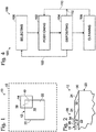
- Fig. 1 schematically illustrates a system 10 associated with methods according to the present disclosure.
- a system 10 may include one or more of a wear part 12, a control structure 14, and a deposition machine 16.
- Wear parts 12 include any suitable wear parts, for which a specific coating profile is desired or predetermined.
- wear parts 12 may include (but are not limited to) one or more of fasteners, bushings, bearing carriers, sleeves, and/or pins.
- Wear parts 12 utilized in the aerospace industry may include parts associated with landing gear systems, flap and actuator systems, or any other systems that include parts that typically require replacement over time.
- wear parts 12 according to the present disclosure are not limited to wear parts utilized in the aerospace industry, and wear parts 12 may be utilized within assemblies associated with such illustrative, non-exclusive examples as aircraft, automobiles, spacecraft, trains, machine tools, robots, manufacturing machines, drilling equipment, pumping equipment, energy generation equipment, vibration absorption equipment, and any other suitable mechanical assembly.
- Wear parts 12 may include a coating or plating 18 that is applied utilizing a deposition process.
- the coating or plating 18 may be a protective layer on the wear part 12.
- a wear part 12 may be described in terms of before and after a coating 18 is applied.
- a wear part may be described in terms of having a body 20 that includes at least one surface 22, on which the coating 18 is applied, adhered, or otherwise bonded to.
- some wear parts 12 may include a multi-layered coating, such as schematically illustrated in Fig. 2 in dash-dot-dot lines. The schematic representation in Fig.
- materials that may be used for one or more layers of a coating 18 include materials selected for adhesion properties, for stress control properties, for durability properties, and/or for ductility properties. Some coatings may be described as multi-layered films for enhancing ductility and/or durability properties. Other types of coatings and optional layers of coatings also are within the scope of the present disclosure.
- Illustrative, non-exclusive examples of materials from which a wear part body 20 may be constructed include (but are not limited to) steel, high-strength steel, stainless steel, aluminum, aluminum alloy, titanium, titanium alloy, nickel, nickel alloy, molybdenum, and molybdenum alloy, as well as non-metallic materials, such as thermoplastics.
- Illustrative, non-exclusive examples of materials of coating 18 include (but are not limited to) nitride based wear coating materials and diamond-like carbon. In addition to nitride based wear coating materials and diamond-like carbon, any materials that may be deposited onto body 20 utilizing a deposition process may be used for a coating 18.
- the deposition process is a is plasma-enhanced chemical vapor deposition (PECVD) process.
- PECVD plasma-enhanced chemical vapor deposition
- materials that may be deposited as a coating 18 include (but are not limited to) silicon dioxide (from dichlorosilane, silane, tetraethoxysilane, cyclic organosilanes), silicon nitrides (silane + ammonia or nitrogen), silicon oxy-nitrides, silicon carbide, carbon nanotubes & buckminster fullerenes, silicon-germanium, molybdenum, tantalum, titanium, nickel, tungsten, indium phosphide, trimethylaluminium (TMA or TMAI), triethylaluminium (TEA or TEAl), trimethylgallium (TMG or TMGa), triethylgallium (TEG or TEGa), trimethylindium (TMI or TMIn), triethylindium
- coating 18 may include a transition region 24, in which the thickness of the coating is different and in some embodiments varies from a region of generally uniform thickness 26.
- the transition region 24 may taper, slope, or diminish away from the region of generally uniform thickness 26.
- the transition region 24 may taper from the thickness of the region of generally uniform thickness 26 to zero.
- the region of generally uniform thickness 26 additionally or alternatively in some embodiments may be described as a region of maximum thickness of coating 18.
- Transition region 24 additionally or alternatively may be referred to as run-out, run-off, a run-out region, a run-off region, and/or as a region of reduced thickness, for example, in embodiments in which the transition region tapers away from the region of generally uniform thickness 26.
- the transition region 24 and the region of generally uniform thickness 26 may be described as defining a coating profile 28 of the wear part 12, or alternatively of the coating 18, for example, with the coating profile 28 representing specific thicknesses, contours, slopes, and/or positions of region 24 and region 26 relative to each other and relative to body 20 of the wear part. Transition region 24 may be important in some applications, so as to reduce the fatigue properties and stress concentrations associated with a portion of a wear part 12.
- the transition region 24 of coating 18 may be adjacent to an edge 30 of the body 20 of a wear part 12. Additionally or alternatively, in some embodiments, the transition region 24 may be described as being positioned on, or within, an edge region 32 of the body 20 of a wear part 12. In solid lines in Fig. 2 , transition region 24 is schematically illustrated as spanning the entirety of an edge region 32 from the region of generally uniform thickness 26 to an edge 30 of the wear part's body 20. However, as schematically illustrated in dashed lines in Fig. 2 , a transition region 24 may terminate at a point that is spaced away from an edge 30 of the wear part's body 20.
- transition region 24 still may be described as being adjacent to the edge 30, for example, because it is adjacent to the edge 30 relative to the region of generally uniform thickness 26.
- Other configurations are within the scope of the present disclosure, including embodiments of wear parts 12 in which a transition region 24 is not adjacent to an edge 30 of a wear part body relative to a region of generally uniform thickness 26.
- Illustrative, non-excusive examples of thicknesses associated with a region of generally uniform thickness 26 include thicknesses in the range of about 0.3-5 mils, including thicknesses in the range of about 0.3-1 mils and in the range of about 0.8-3 mils, and including thicknesses greater than 0.3, 0.5, 0.75, 1, 1.5, 2, 2.5, 3, 3.5, 4, 4.5, or 5 mils. Thicknesses less than, greater than, and within the various enumerated values herein are within the scope of the present disclosure.
- PECVD processes were used to deposit coatings with thicknesses less than 0.3 mil. Because coatings of such thinness typically do not create stress concentrations associated with the edges of the coatings, defining a predetermined run-out profile associated with coatings less than 0.3 mil generally has not been needed.
- the aspect ratio of the layers within the transition region 24 may be maintained, although such a limitation is not required to all embodiments.
- a deposition process may facilitate the maintaining of the aspect ratios associated with optional multi-layer coatings.
- a wear part 12 may be a replacement part, with the wear part 12 having a configuration corresponding to a desired or predetermined coating profile 28 that is associated with a part being replaced.
- a wear part 12 according to the present disclosure may be a replacement part that is specifically designed, configured, manufactured, produced, and/or coated to have a coating profile 28 that corresponds to, is identical to, and/or is nearly identical to a coating profile of the part being replaced.
- the coating of the wear part 12 may be of a different material than the coating of a part being replaced.
- Examples of a part that may be replaced by a wear part include parts that have a coating, or plating, with a specific coating, or plating, profile.
- chrome plating including hard chrome, industrial chrome, and/or engineering chrome plating having thicknesses corresponding to standard chrome plating (1-5 mil thickness) or thin dense chrome plating (0.3-1 mil thickness) may correspond to a part being replaced.
- Additional illustrative, non-exclusive examples of coatings associated with a part being replaced include (but are not limited to) coatings that have a potential for environmental impact, such as coatings that include material on an Environmental Protection Agency (EPA) watch list (e.g., nickel).
- EPA Environmental Protection Agency
- Other examples of parts that may be replaced by a wear part 12 are within the scope of the present disclosure, including parts that do not have a plating or coating and parts that have a plating or coating that include a material other than the materials identified herein.
- Control structures 14 include any suitable structure that may be utilized to create a desired or predetermined coating profile 28 of a wear part 12.
- control structure 14 is schematically illustrated as being positioned relative to wear part 12, with such representation schematically representing any suitable relative positioning between a wear part 12 and a control structure 14 during a process for applying a coating 18.
- a control structure 14 may be positioned in any suitable position, depending on the configuration of the control structure 14, depending on the configuration of the wear part 12, depending on the configuration of a desired or predetermined coating profile associated with a wear part 12, and/or depending on the process used to apply a coating 18.
- Fig. 1 control structure 14 is schematically illustrated as being positioned relative to wear part 12, with such representation schematically representing any suitable relative positioning between a wear part 12 and a control structure 14 during a process for applying a coating 18.
- a control structure 14 may be positioned in any suitable position, depending on the configuration of the control structure 14, depending on the configuration of the wear part 12, depending on the configuration of a desired or predetermined coating profile associated with a wear part 12,
- the relative position between the control structure 14 and a wear part 12 may define a region 40, for example, with such region being defined by, or defining, a volume of space between the control structure and the wear part.
- Region 40 additionally or alternatively may define a region associated with deposition of a transition region 24 of a coating 18.
- a coating 18 is applied to a wear part 12 utilizing a deposition process using a plasma-enhanced chemical vapor deposition (PECVD) machine, for example including an ion-assisted PECVD machine.
- PECVD is a process that deposits material from a gaseous, plasma state to a solid state on a substrate, by imparting an electric potential between the substrate and an inside surface of the deposition chamber, with the substrate and the inside surface of the deposition chamber serving as electrodes. Accordingly, ions and/or radicals of the material being deposited bombard the substrate and are thus deposited thereon.
- a control structure 14 may be described as being specifically configured to be positioned relative to a wear part 12, or to the body 20 of a wear part 12, or to a wear part surface 22, to define a region of reduced electric field 38 adjacent to a portion of the wear part on which a less thickness of deposited material is desired.
- Fig. 3 schematically represents illustrative, non-exclusive examples of control structure 14 in the form of a masking jig 42.
- Masking jig 42 additionally or alternatively may be referred to as a fixture 42 or as a masking fixture 42.
- the masking jig is positioned relative to a wear part 12 to define a volume 44 between the masking jig 42 and the surface 22 of the wear part 12 to be coated with a coating 18.
- masking jig 42 may be described as including an overhang 46 that is configured to extend over the edge region 32 of the wear part's body 20, with the position of the overhang 46 defining the volume 44 between the overhang 46 and the edge region 32.
- region 40 may be described as a region of reduced electric field 38 within the volume 44 defined between the masking jig and the wear part surface 22. This reduced electric field results in less material being deposited on the wear part surface within the region of the reduced electric field 38, and specifically with less material the deeper into the volume that material is deposited, thus resulting in run-out.
- the reduction in the electric field in region 40 is a result of a decreased potential gradient.
- the potential drops near the surface of the substrate (e.g., wear part 12), which serves as a cathode.
- the two equal potential surfaces i.e., the surface 22 and the overhang surface 48
- the electric field gradient is directly proportional to the potential gradient, the electric field also decreases.
- the deposition rate is dependent on the local field, because the radicals used to coat the substrate are ions, which accelerate toward the surface due to the electric field. Accordingly, the deposition rate is decreased when the electric field is decreased, resulting in less deposition on the substrate in the region of reduced electric field 38.
- Masking jigs 42 therefore may be configured, or otherwise customized or specifically designed, to result in a desired or predetermined coating profile 28 associated with a wear part 12.
- One or more of the size, shape, material of the masking jig, and/or the positioning of the masking jig 42 relative to the wear part surface 22 may be selected to manipulate, or control, the coating profile 28 produced during a deposition process.
- the shape of the volume 44 between the masking jig 42 and the wear part surface 22 may be preselected to define a desired or predetermined coating profile 28.
- the same masking jig 42 may be used to deposit each layer of the coating without removal or cleaning of the masking jig 42. As discussed, such a process may result in an aspect ratio of the layers being maintained between the transition region 24 and the region of generally uniform thickness 26.
- overhang 46 may define an overhang surface 48 that has a contour that corresponds to the edge region 32 of the wear part surface 22.
- the overhang surface 48 may be generally parallel to the wear part surface 22 when the overhang 46 is positioned in a spaced-apart position relative to the wear part surface 22 for use during deposition of a coating 18.
- Other configurations also are within the scope of the present disclosure, with two illustrative, non-exclusive examples of overhang surfaces 48 schematically illustrated in Fig. 3 in dash-dot and dash-dot-dot lines and having slopes relative to the wear part surface 22.
- the appropriate positioning of the masking jig 42 relative to the wear part surface 22 for a desired or predetermined coating profile 28 may result in a gap 52 in the range of 10-500, 10-200, 10-100, 10-50, 50-500, 50-200, 50-100, 100-500, 100-200, or 200-500 mils between the overhang 46 and the wear part surface 22.
- Any suitable gap including gaps that are less than, greater than, and within the enumerated values, are within the scope of the present disclosure and may be used to produce a desired or predetermined coating profile 28.
- the length of overhang 46 may be selected together with the gap 52 to define a desired or predetermined coating profile 28.
- suitable lengths of overhangs 46 include (but are not limited to) lengths in the range of 10-1000, 10-800, 10-600, 10-400, 10-200, 200-1000, 200-800, 200-600, 200-400, 400-1000, 400-800, 400-600, 600-1000, 600-800, and 800-1000 mils, as well as lengths greater than 10, 200, 400, 600, 800, or 1000 mils. Lengths less than, greater than, and within the various enumerated values are within the scope of the present disclosure and may be used to produce a desired or predetermined coating profile 28.
- masking jig 42 is schematically illustrated as being engaged with wear part 12, but such a configuration is not required in all methods according to the present disclosure, and in some configurations, the masking jig 42 may not engage the wear part 12 being coated during a deposition process.
- Masking jigs 42 may be constructed of any suitable material, such that use of a masking jig results in a desired or predetermined coating profile.
- a masking jig may be constructed at least partially, and in some embodiments at least predominantly or completely, of a conductive material.
- at least a portion of an outer surface of the masking jig, such as (but not limited to) corresponding to at least the overhang surface 48, may be constructed of, or include, a conductive material.
- the masking jig may serve as an electrode during the deposition process.
- the masking jig 42 and the wear part 12 may have an equal potential during the deposition process.
- the material of the coating 18 also may be deposited on the masking jig 42, as schematically and optionally indicated at 54 in Fig. 3 .
- Fig. 4 schematically provides a flowchart that represents illustrative, non-exclusive examples of methods according to the present disclosure.
- some steps are illustrated in dashed boxes indicating that such steps may be optional or may correspond to an optional version of a method according to the present disclosure. That said, not all methods according to the present disclosure are required to include the steps illustrated in solid boxes.
- the methods and steps illustrated in Fig. 4 are not limiting and other methods and steps are within the scope of the present disclosure, including methods having greater than or fewer than the number of steps illustrated, as understood from the discussions herein.
- Fig. 4 schematically illustrates a method 100 of coating a wear part surface 22 according to a desired or predetermined coating profile 28.
- Methods 100 according to the present disclosure include the positioning of a control structure 14 relative to a wear part 12, as indicated at 102, and then after the positioning, include the depositing of a material on the wear part surface 22 of the wear part 12, as indicated at 104.
- Positioning 102 includes positioning the masking jig 42 relative to the wear part 12 to define a volume 44 between the masking jig 42 and the wear part surface 22.
- the depositing 104 includes depositing the coating material utilizing a plasma-enhanced chemical vapor deposition (PECVD) process, in which the position of the masking jig 42 relative to the wear part surface defines the region of reduced electric field 38 so that a transition region 24 is deposited on the portion of the wear part surface 22 that bounds volume 44.
- PECVD plasma-enhanced chemical vapor deposition
- Some methods 100 may include utilizing ion-assisted PECVD.
- Some methods 100 additionally or alternatively may include a step of selecting an appropriate control structure or masking jig 42, as indicated at 106, to define a desired or predetermined coating profile 28 on a wear part 12.
- the masking jig 42 may need to be cleaned of deposited material, as indicated at 108. Such a step may be required because the material being deposited on the wear part surface 22 also will be deposited on the masking jig 42, and if the masking jig 42 is to be used again, the deposited material may need to be removed, so that method 100 may be repeated, as schematically indicated at 110. Additionally or alternatively, a used masking jig 42 may be disposed of, or otherwise not used again.
- a masking jig 42 may be used more than once without cleaning, as schematically indicated in Fig. 4 at 112.
- cleaning processes 108 include (but are not limited to) abrasive processes, such as sand-blasting, chemical processes, etching processes, laser ablation, and dissolution processes.
- a new masking jig may be selected that is different from the first masking jig that was used. Additionally or alternatively, the first masking jig may be altered. In such methods, the new or altered masking jig may be selected based at least in part on observing the coating profile 28 produced with the first masking jig and comparing the coating profile 28 to a desired coating profile.
- the new or altered masking jig may define a volume 44 between the second masking jig and the second wear part surface that is different than the volume 44 that was defined between the first masking jig and the first wear part surface.
- methods 120 may be performed to design a desired masking jig for manufacturing replacement wear parts that have a coating profile that corresponds to a coating profile 28 of the part being replaced by the replacement parts.
- a method of designing a custom masking jig for creating a desired coating profile on a wear part may include modeling, with a computer, one or more steps of a method according to the present disclosure, including a method 100 or a method 120.
- software such as embodied by computer-executable instructions, may direct a computer to perform one or more steps of a method according to the present disclosure, and is within the scope of the present disclosure.
- This example describes an illustrative, non-exclusive example of a utilization of a method according to the present disclosure to deposit a coating on a substrate with the resultant coating having a run-out.
- Fig. 5 shows a schematic representation of a cross-sectional profile of a substrate 60, which may correspond to a wear part 12 according to the present disclosure, together with an illustrative, non-exclusive example of a masking jig 62 that was constructed for purposes of the test.
- the dimensions of the substrate 60 and the masking jig 62 are indicated in Fig. 5 in inches. Both the substrate 60 and the masking jig 62 were constructed of titanium.
- the substrate 60 and masking jig 62 were placed in the chamber of a plasma-enhanced chemical vapor deposition (PECVD) machine, and a coating of diamond-like carbon with a thickness of approximately 1 mil was applied.
- PECVD plasma-enhanced chemical vapor deposition
- Fig. 6 graphically represents the profilometry data and therefore graphically represents the resultant coating profile of the applied coating. As seen in the region between the two vertically orientated dashed lines, the resultant coating profile includes a region of run-out, which tapers approximately 1 mil in thickness over a width of approximately 0.1 inches.
- a method is disclosed of coating a wear part surface 22, the method comprising positioning a masking jig 42, 62 relative to a wear part 12, wherein the wear part 12 includes a wear part surface 22 to be coated, and wherein the positioning generally defines a volume 44 between the masking jig 42, 62 and the wear part surface 22; and after the positioning, depositing a deposited material to the wear part surface 22 utilizing chemical vapor deposition, in which the position of the masking jig 42, 62 relative to the wear part surface 22 defines a region of reduced electric field 38 within the volume 44 between the masking jig 42, 62 and the wear part surface 22, wherein the deposited material defines a coating profile 28.
- the method includes wherein the coating profile 28 is a predetermined coating profile 28.
- the method includes wherein the predetermined coating profile 28 corresponds to a part (12) to be replaced by the wear part 12.
- the method includes wherein the wear part 12 includes a bushing, a bearing carrier, a pin, a fastener, a sleeve, landing gear hardware, flap hardware, or actuator hardware.
- the method includes wherein the wear part 12 to be replaced includes a chrome plating. In another instance, the method includes wherein the predetermined coating profile 28 includes a tapered region that is adjacent to an edge of the wear part surface 22.
- the method includes wherein the masking jig 42, 62 includes an overhang 46; and wherein the positioning includes: positioning the overhang 46 in a spaced-apart position relative to the wear part surface 22 to be coated to define the volume 44 between the masking jig 42, 62 and the wear part surface 22.
- the method includes wherein the overhang 46 defines an overhang surface 48 that has a contour corresponding to an edge region 32 of the wear part surface 22.
- the method includes wherein the overhang surface 48 is generally parallel to the wear part surface 22 when the overhang 46 is positioned in the spaced-apart position.
- the method includes wherein a shape of the volume 44 between the masking jig 42, 62 and the wear part surface 22 is preselected to define a predetermined coating profile 28 on the wear part surface 22.
- the method includes wherein the masking jig 42, 62 is a custom masking jig 42, 62 configured specifically for use with the wear part 12.
- the method includes wherein the depositing results in a thickness of the deposited material on a portion of the wear part surface 22 that does not bound the volume 44 between the masking jig 42, 62 and the wear part surface 22 that is between about 0.3 and 5 mils.
- the method includes wherein the wear part 12 is a replacement part 12 for a part 12 being replaced and having a configuration corresponding to the wear part 12 after the depositing, and wherein the deposited material is different than a coating material of the part 12 being replaced.
- the method includes wherein the depositing includes depositing a multi-layered coating.
- the method includes wherein the deposited material includes at least one of nitride based wear coating material and diamond-like carbon.
- a method is disclosed of designing a custom masking jig 42, 62 for creating a desired coating profile 28 on a wear part 12 utilizing a plasma-enhanced chemical vapor deposition process, the method including modeling, with a computer, the method of coating a wear part surface 22, the method including positioning a masking jig 42, 62 relative to a wear part 12, wherein the wear part 12 includes a wear part surface 22 to be coated, and wherein the positioning generally defines a volume 44 between the masking jig 42, 62 and the wear part surface 22; and after the positioning, depositing a deposited material to the wear part surface 22 utilizing chemical vapor deposition, in which the position of the masking jig 42, 62 relative to the wear part surface 22 defines a region of reduced electric field 38 within the volume 44 between the masking jig 42, 62 and the wear part surface 22, wherein the deposited material defines a coating profile 28.
- the method includes wherein the coating profile 28 is a predetermined coating profile 28. In another example, the method includes wherein the predetermined coating profile 28 corresponds to a part 12 to be replaced by the wear part 12. In yet another example, the method includes wherein the wear part 12 includes a bushing, a bearing carrier, a pin, a fastener, a sleeve, landing gear hardware, flap hardware, or actuator hardware.
- a coated wear part 12 is produced utilizing the method of coating a wear part surface 22, the method including positioning a masking jig 42, 62 relative to a wear part 12, wherein the wear part 12 includes a wear part surface 22 to be coated, and wherein the positioning generally defines a volume 44 between the masking jig 42, 62 and the wear part surface 22; and after the positioning, depositing a deposited material to the wear part surface 22 utilizing chemical vapor deposition, in which the position of the masking jig 42, 62 relative to the wear part surface 22 defines a region of reduced electric field 38 within the volume 44 between the masking jig 42, 62 and the wear part surface 22, wherein the deposited material defines a coating profile 28.
- the method includes wherein the coating profile 28 is a predetermined coating profile 28. In another example, the method includes wherein the predetermined coating profile 28 corresponds to a part 12 to be replaced by the wear part 12. In yet another example, the method includes wherein the wear part 12 includes a bushing, a bearing carrier, a pin, a fastener, a sleeve, landing gear hardware, flap hardware, or actuator hardware.
- a method is disclosed of coating a wear part surface 22, including: depositing a deposited material to the wear part surface 22 utilizing plasma-enhanced chemical vapor deposition; and controlling the depositing to define a predetermined coating profile 28 on the wear part surface 22, wherein a predetermined coating profile 28, e.g., desired coating profile 28, includes a region of substantially uniform thickness of the deposited material and one or more regions of tapered thicknesses of the deposited material adjacent to one or more edges of the wear part surface 22.
- a method is disclosed of coating a wear part surface 22, including: depositing a deposited material to the wear part surface 22 utilizing plasma-enhanced chemical vapor deposition, during which an electric field 50 is induced adjacent to the wear part surface 22; and controlling the electric field 50 to produce a predetermined coating profile 28 associated with the wear part 12.
- the method includes wherein the controlling includes positioning a control structure relative to the wear part surface 22.
- a control structure 14 in a form of a custom masking jig 42, 62 for creating a desired coating profile 28 on a wear part 12 utilizing a plasma-enhanced chemical vapor deposition process comprising: a masking jig 42, 62 positioned relative to a wear part 12 that generally defines a volume 44 between the masking jig 42, 62 and a wear part surface 22 of the wear part 12 to be coated and positioned to deposit material to the wear part surface 22 utilizing chemical vapor deposition, wherein the position of the masking jig 42, 62 relative to the wear part surface 22 defines a region of reduced electric field 38 within the volume 44 between the masking jig 42, 62 and the wear part surface 22 and the deposited material defines a coating profile 28.
- control structure 14 includes wherein the masking jig 42, 62 includes an overhang 46 positioned in a spaced-apart position relative to the wear part surface 22 to be coated and to define the volume 44 between the masking jig 42, 62 and the wear part surface 22.
- adapted and “configured” mean that the element, component, or other subject matter is designed and/or intended to perform a given function.
- the use of the terms “adapted” and “configured” should not be construed to mean that a given element, component, or other subject matter is simply “capable of” performing a given function but that the element, component, and/or other subject matter is specifically selected, created, implemented, utilized, programmed, and/or designed for the purpose of performing the function.
- elements, components, and/or other recited subject matter that is recited as being adapted to perform a particular function may additionally or alternatively be described as being configured to perform that function, and vice versa.
Landscapes
- Chemical & Material Sciences (AREA)
- Mechanical Engineering (AREA)
- General Chemical & Material Sciences (AREA)
- Chemical Kinetics & Catalysis (AREA)
- Engineering & Computer Science (AREA)
- Materials Engineering (AREA)
- Metallurgy (AREA)
- Organic Chemistry (AREA)
- Inorganic Chemistry (AREA)
- Chemical Vapour Deposition (AREA)
- Physical Vapour Deposition (AREA)
- Sliding-Contact Bearings (AREA)
- Laminated Bodies (AREA)
- Application Of Or Painting With Fluid Materials (AREA)
Claims (14)
- Verfahren zum Beschichten einer Oberfläche (22) eines Teils (12), wobei das Verfahren umfasst:Positionieren einer Maskierungslehre (42, 62) relativ zu dem Teil (12), und dadurch Definieren eines Volumens (44) zwischen der Maskierungslehre (42, 62) und der Oberfläche (22); undnach dem Positionieren, Abscheiden eines Abscheidematerials auf der Oberfläche (22) unter Verwendung von plasmaverstärkter chemischer Dampfabscheidung, wobei die Position der Maskierungslehre (42, 62) relativ zur Oberfläche (22) einen Bereich eines verringerten elektrischen Feldes (38) innerhalb des Volumens (44) zwischen der Maskierungslehre (42, 62) und der Oberfläche (22) definiert, wobei das abgeschiedene Material ein Beschichtungsprofil (28) definiert, das einen sich verjüngenden Bereich umfasst.
- Verfahren nach einem der Ansprüche 1, bei dem das Beschichtungsprofil (28) einem durch das Teil (12) zu ersetzenden Teil entspricht.
- Verfahren nach einem der Ansprüche 1 bis 2, bei dem das Teil (12) eine Buchse, einen Lagerträger, einen Bolzen, ein Befestigungsmittel, eine Hülse, Fahrwerkshardware, Klappenhardware oder Betätigungshardware umfasst.
- Verfahren nach Anspruch 2, bei dem das zu ersetzende Teil (12) eine Verchromung aufweist.
- Verfahren nach Anspruch 2 oder Anspruch 3, bei dem der sich verjüngende Bereich an eine Kante der Oberfläche (22) des Verschleißteils angrenzt.
- Verfahren nach einem der Ansprüche 1-4,bei dem die Maskierungslehre (42, 62) einen Überhang (46) aufweist; undwobei das Positionieren umfasst:
Positionieren des Überhangs (46) in einer beabstandeten Position relativ zu der zu beschichtenden Oberfläche (22), um das Volumen (44) zwischen der Maskierungslehre (42, 62) und der Oberfläche (22) zu definieren. - Verfahren nach Anspruch 6, bei dem der Überhang (46) eine Überhangoberfläche (48) definiert, die eine einem Randbereich (32) der Oberfläche (22) des Teils (12) entsprechende Kontur aufweist.
- Verfahren nach Anspruch 7, bei dem die Überhangoberfläche (48) allgemein parallel zur Oberfläche (22) ist, wenn der Überhang (46) in der beabstandeten Position positioniert ist.
- Verfahren nach einem der Ansprüche 1-4, bei dem eine Form des Volumens (44) zwischen der Maskierungslehre (42, 62) und der Oberfläche (22) des Verschleißteils vorgewählt wird, um das Beschichtungsprofil (28) auf der Oberfläche (22) zu definieren.
- Verfahren nach einem der Ansprüche 1-9, bei dem die Maskierungslehre (42, 62) eine maßgefertigte Maskierungslehre (42, 62) ist, die speziell für die Verwendung mit dem Teil (12) konfiguriert ist.
- Verfahren nach einem der Ansprüche 1-9, bei dem das Abscheiden auf einem Abschnitt der Oberfläche (22), der das Volumen (44) zwischen der Maskierungsvorrichtung (42, 62) und der Oberfläche (22) nicht begrenzt, zu einer Dicke des abgeschiedenen Materials führt, die zwischen etwa 0,3 und 5 mils (= 7,6 und 127 Mikrometer) liegt.
- Verfahren nach einem der Ansprüche 1 und 2-11, bei dem das Teil (12) ein Ersatzteil (12) für ein Teil (12) ist, das ersetzt wird, und nach dem Abscheiden eine Konfiguration aufweist, die dem Teil (12) entspricht, und bei dem das abgeschiedene Material sich von einem Beschichtungsmaterial des zu ersetzenden Teils (12) unterscheidet.
- Verfahren nach einem der Ansprüche 1-12, bei dem das Abscheiden das Abscheiden einer mehrschichtigen Beschichtung umfasst.
- Verfahren nach einem der Ansprüche 1-13, bei dem das abgeschiedene Material mindestens ein Verschleißbeschichtungsmaterial auf Nitridbasis oder diamantähnlichen Kohlenstoff enthält.
Applications Claiming Priority (1)
| Application Number | Priority Date | Filing Date | Title |
|---|---|---|---|
| US13/414,022 US9297068B2 (en) | 2012-03-07 | 2012-03-07 | Wear parts having coating run-out and methods of producing same |
Publications (3)
| Publication Number | Publication Date |
|---|---|
| EP2636766A2 EP2636766A2 (de) | 2013-09-11 |
| EP2636766A3 EP2636766A3 (de) | 2016-09-21 |
| EP2636766B1 true EP2636766B1 (de) | 2020-02-26 |
Family
ID=47832952
Family Applications (1)
| Application Number | Title | Priority Date | Filing Date |
|---|---|---|---|
| EP13157673.8A Active EP2636766B1 (de) | 2012-03-07 | 2013-03-04 | Verschleißteile mit Beschichtungsauslauf und Verfahren zur Herstellung davon |
Country Status (4)
| Country | Link |
|---|---|
| US (1) | US9297068B2 (de) |
| EP (1) | EP2636766B1 (de) |
| JP (1) | JP5507712B2 (de) |
| CN (1) | CN103305805B (de) |
Families Citing this family (3)
| Publication number | Priority date | Publication date | Assignee | Title |
|---|---|---|---|---|
| US9441305B2 (en) * | 2014-01-03 | 2016-09-13 | The Boeing Company | Composition and method for inhibiting corrosion |
| AT15974U1 (de) * | 2016-09-01 | 2018-10-15 | Miba Gleitlager Austria Gmbh | Verfahren zur Herstellung eines Mehrschichtgleitlagerelementes |
| CN107119262A (zh) * | 2017-05-27 | 2017-09-01 | 华南理工大学 | 一种镍金属基体表面催化生长碳纳米管薄膜的方法 |
Family Cites Families (22)
| Publication number | Priority date | Publication date | Assignee | Title |
|---|---|---|---|---|
| US4159222A (en) * | 1977-01-11 | 1979-06-26 | Pactel Corporation | Method of manufacturing high density fine line printed circuitry |
| US4447904A (en) * | 1981-02-04 | 1984-05-08 | Xerox Corporation | Semiconductor devices with nonplanar characteristics produced in chemical vapor deposition |
| JPH0815152B2 (ja) * | 1986-01-27 | 1996-02-14 | 三菱電機株式会社 | 半導体装置及びその製造方法 |
| US5851911A (en) * | 1996-03-07 | 1998-12-22 | Micron Technology, Inc. | Mask repattern process |
| US6277198B1 (en) * | 1999-06-04 | 2001-08-21 | Applied Materials, Inc. | Use of tapered shadow clamp ring to provide improved physical vapor deposition system |
| US6482264B1 (en) * | 2000-10-26 | 2002-11-19 | General Electric Company | Systems and methods for fabrication of coating libraries |
| KR100512988B1 (ko) * | 2002-09-26 | 2005-09-07 | 삼성전자주식회사 | 플렉서블 mems 트랜스듀서 제조방법 |
| US7291360B2 (en) * | 2004-03-26 | 2007-11-06 | Applied Materials, Inc. | Chemical vapor deposition plasma process using plural ion shower grids |
| US7444955B2 (en) | 2004-05-19 | 2008-11-04 | Sub-One Technology, Inc. | Apparatus for directing plasma flow to coat internal passageways |
| US7300684B2 (en) | 2004-07-15 | 2007-11-27 | Sub-One Technology, Inc. | Method and system for coating internal surfaces of prefabricated process piping in the field |
| US7335398B2 (en) * | 2004-07-26 | 2008-02-26 | Asml Holding N.V. | Method to modify the spatial response of a pattern generator |
| US7541069B2 (en) | 2005-03-07 | 2009-06-02 | Sub-One Technology, Inc. | Method and system for coating internal surfaces using reverse-flow cycling |
| US7608151B2 (en) | 2005-03-07 | 2009-10-27 | Sub-One Technology, Inc. | Method and system for coating sections of internal surfaces |
| CN100516291C (zh) * | 2005-10-14 | 2009-07-22 | 中微半导体设备(上海)有限公司 | 等离子体处理装置 |
| US8703240B2 (en) * | 2005-10-18 | 2014-04-22 | American Axle & Manufacturing, Inc. | Apparatus and method for masking and coating tool blades |
| US7626135B2 (en) | 2006-05-10 | 2009-12-01 | Sub-One Technology, Inc. | Electrode systems and methods of using electrodes |
| TWI431380B (zh) * | 2006-05-12 | 2014-03-21 | 光子動力公司 | 沉積修復設備及方法 |
| US7838793B2 (en) | 2006-07-21 | 2010-11-23 | Sub-One Technology, Inc. | System and method for treating surfaces of components |
| US8568827B2 (en) * | 2006-11-30 | 2013-10-29 | Caterpillar Inc. | Textured coating on a component surface |
| US7629031B2 (en) | 2007-07-13 | 2009-12-08 | Sub-One Technology, Inc. | Plasma enhanced bonding for improving adhesion and corrosion resistance of deposited films |
| US8431495B2 (en) * | 2010-07-08 | 2013-04-30 | Varian Semiconductor Equipment Associates, Inc. | Stencil mask profile |
| JP5665409B2 (ja) * | 2010-08-06 | 2015-02-04 | 株式会社ジェイテクト | 被膜の成膜方法 |
-
2012
- 2012-03-07 US US13/414,022 patent/US9297068B2/en not_active Expired - Fee Related
-
2013
- 2013-01-09 JP JP2013001458A patent/JP5507712B2/ja not_active Expired - Fee Related
- 2013-03-04 EP EP13157673.8A patent/EP2636766B1/de active Active
- 2013-03-04 CN CN201310067129.XA patent/CN103305805B/zh not_active Expired - Fee Related
Non-Patent Citations (1)
| Title |
|---|
| None * |
Also Published As
| Publication number | Publication date |
|---|---|
| JP2013185257A (ja) | 2013-09-19 |
| EP2636766A3 (de) | 2016-09-21 |
| EP2636766A2 (de) | 2013-09-11 |
| JP5507712B2 (ja) | 2014-05-28 |
| CN103305805A (zh) | 2013-09-18 |
| CN103305805B (zh) | 2018-06-26 |
| US9297068B2 (en) | 2016-03-29 |
| US20130236704A1 (en) | 2013-09-12 |
Similar Documents
| Publication | Publication Date | Title |
|---|---|---|
| EP2676790A1 (de) | Gleitelement und herstellungsverfahren dafür | |
| EP2636766B1 (de) | Verschleißteile mit Beschichtungsauslauf und Verfahren zur Herstellung davon | |
| US10483092B2 (en) | Baffle plate and showerhead assemblies and corresponding manufacturing method | |
| US10468289B2 (en) | Substrate holding member | |
| CN103567912A (zh) | 吸附平台的制造方法及吸附平台 | |
| SG11201803914QA (en) | Method for Epitaxially Coating Semiconductor Wafers, and Semiconductor Wafer | |
| MX2021005871A (es) | Artículos de vidrio con recubrimientos resistentes a daños y métodos para recubrir artículos de vidrio. | |
| KR20200003194A (ko) | 서셉터, 애피택셜 기판의 제조 방법, 및 애피택셜 기판 | |
| EP2824214B1 (de) | Beschichtungsanordnung für Kraftstoffeinspritzregelventil und Verfahren | |
| US20140174917A1 (en) | Recycling Method for Tantalum Coil for Sputtering and Tantalum Coil Obtained by the Recycling Method | |
| CN109554663A (zh) | 蒸镀掩模、带框架的蒸镀掩模、及它们的制造方法 | |
| TWI752374B (zh) | 成膜構造體的再生方法及再生成膜構造體 | |
| CN110088351A (zh) | 用于给金属构件涂覆磨损保护层的方法、金属构件以及燃料喷射系统 | |
| JP2007258154A (ja) | イオン注入装置 | |
| US20200243302A1 (en) | SiC MEMBER AND MANUFACTURING METHOD THEREOF | |
| JP6402727B2 (ja) | 溶射用マスキング装置 | |
| KR101574073B1 (ko) | 샤워 헤드 가공 방법 | |
| JP6460659B2 (ja) | セラミック部材 | |
| US20140097157A1 (en) | Combined method for drilling a layer system, in which mechanical working and edm working are performed | |
| US10903076B2 (en) | Material selective regrowth structure and method | |
| US20180218890A1 (en) | Sputtering coil product and method of making | |
| CN102768964A (zh) | 制造半导体部件的方法 | |
| US10131007B2 (en) | Cutting tool and method for its manufacture | |
| US11230762B2 (en) | Film structure reproduction method and reproduction film structure | |
| US9181618B2 (en) | Magnetic layer patterning by ion implantation |
Legal Events
| Date | Code | Title | Description |
|---|---|---|---|
| PUAI | Public reference made under article 153(3) epc to a published international application that has entered the european phase |
Free format text: ORIGINAL CODE: 0009012 |
|
| 17P | Request for examination filed |
Effective date: 20130304 |
|
| AK | Designated contracting states |
Kind code of ref document: A2 Designated state(s): AL AT BE BG CH CY CZ DE DK EE ES FI FR GB GR HR HU IE IS IT LI LT LU LV MC MK MT NL NO PL PT RO RS SE SI SK SM TR |
|
| AX | Request for extension of the european patent |
Extension state: BA ME |
|
| PUAL | Search report despatched |
Free format text: ORIGINAL CODE: 0009013 |
|
| AK | Designated contracting states |
Kind code of ref document: A3 Designated state(s): AL AT BE BG CH CY CZ DE DK EE ES FI FR GB GR HR HU IE IS IT LI LT LU LV MC MK MT NL NO PL PT RO RS SE SI SK SM TR |
|
| AX | Request for extension of the european patent |
Extension state: BA ME |
|
| RIC1 | Information provided on ipc code assigned before grant |
Ipc: C23C 16/26 20060101ALI20160812BHEP Ipc: C23C 16/04 20060101AFI20160812BHEP |
|
| STAA | Information on the status of an ep patent application or granted ep patent |
Free format text: STATUS: EXAMINATION IS IN PROGRESS |
|
| 17Q | First examination report despatched |
Effective date: 20190315 |
|
| GRAP | Despatch of communication of intention to grant a patent |
Free format text: ORIGINAL CODE: EPIDOSNIGR1 |
|
| STAA | Information on the status of an ep patent application or granted ep patent |
Free format text: STATUS: GRANT OF PATENT IS INTENDED |
|
| INTG | Intention to grant announced |
Effective date: 20190906 |
|
| GRAS | Grant fee paid |
Free format text: ORIGINAL CODE: EPIDOSNIGR3 |
|
| GRAA | (expected) grant |
Free format text: ORIGINAL CODE: 0009210 |
|
| STAA | Information on the status of an ep patent application or granted ep patent |
Free format text: STATUS: THE PATENT HAS BEEN GRANTED |
|
| AK | Designated contracting states |
Kind code of ref document: B1 Designated state(s): AL AT BE BG CH CY CZ DE DK EE ES FI FR GB GR HR HU IE IS IT LI LT LU LV MC MK MT NL NO PL PT RO RS SE SI SK SM TR |
|
| REG | Reference to a national code |
Ref country code: GB Ref legal event code: FG4D |
|
| REG | Reference to a national code |
Ref country code: CH Ref legal event code: EP |
|
| REG | Reference to a national code |
Ref country code: AT Ref legal event code: REF Ref document number: 1237705 Country of ref document: AT Kind code of ref document: T Effective date: 20200315 |
|
| REG | Reference to a national code |
Ref country code: IE Ref legal event code: FG4D |
|
| REG | Reference to a national code |
Ref country code: DE Ref legal event code: R096 Ref document number: 602013066161 Country of ref document: DE |
|
| PG25 | Lapsed in a contracting state [announced via postgrant information from national office to epo] |
Ref country code: FI Free format text: LAPSE BECAUSE OF FAILURE TO SUBMIT A TRANSLATION OF THE DESCRIPTION OR TO PAY THE FEE WITHIN THE PRESCRIBED TIME-LIMIT Effective date: 20200226 Ref country code: NO Free format text: LAPSE BECAUSE OF FAILURE TO SUBMIT A TRANSLATION OF THE DESCRIPTION OR TO PAY THE FEE WITHIN THE PRESCRIBED TIME-LIMIT Effective date: 20200526 Ref country code: RS Free format text: LAPSE BECAUSE OF FAILURE TO SUBMIT A TRANSLATION OF THE DESCRIPTION OR TO PAY THE FEE WITHIN THE PRESCRIBED TIME-LIMIT Effective date: 20200226 |
|
| REG | Reference to a national code |
Ref country code: NL Ref legal event code: MP Effective date: 20200226 |
|
| REG | Reference to a national code |
Ref country code: LT Ref legal event code: MG4D |
|
| PG25 | Lapsed in a contracting state [announced via postgrant information from national office to epo] |
Ref country code: GR Free format text: LAPSE BECAUSE OF FAILURE TO SUBMIT A TRANSLATION OF THE DESCRIPTION OR TO PAY THE FEE WITHIN THE PRESCRIBED TIME-LIMIT Effective date: 20200527 Ref country code: IS Free format text: LAPSE BECAUSE OF FAILURE TO SUBMIT A TRANSLATION OF THE DESCRIPTION OR TO PAY THE FEE WITHIN THE PRESCRIBED TIME-LIMIT Effective date: 20200626 Ref country code: HR Free format text: LAPSE BECAUSE OF FAILURE TO SUBMIT A TRANSLATION OF THE DESCRIPTION OR TO PAY THE FEE WITHIN THE PRESCRIBED TIME-LIMIT Effective date: 20200226 Ref country code: LV Free format text: LAPSE BECAUSE OF FAILURE TO SUBMIT A TRANSLATION OF THE DESCRIPTION OR TO PAY THE FEE WITHIN THE PRESCRIBED TIME-LIMIT Effective date: 20200226 Ref country code: SE Free format text: LAPSE BECAUSE OF FAILURE TO SUBMIT A TRANSLATION OF THE DESCRIPTION OR TO PAY THE FEE WITHIN THE PRESCRIBED TIME-LIMIT Effective date: 20200226 Ref country code: BG Free format text: LAPSE BECAUSE OF FAILURE TO SUBMIT A TRANSLATION OF THE DESCRIPTION OR TO PAY THE FEE WITHIN THE PRESCRIBED TIME-LIMIT Effective date: 20200526 |
|
| PG25 | Lapsed in a contracting state [announced via postgrant information from national office to epo] |
Ref country code: NL Free format text: LAPSE BECAUSE OF FAILURE TO SUBMIT A TRANSLATION OF THE DESCRIPTION OR TO PAY THE FEE WITHIN THE PRESCRIBED TIME-LIMIT Effective date: 20200226 |
|
| PG25 | Lapsed in a contracting state [announced via postgrant information from national office to epo] |
Ref country code: ES Free format text: LAPSE BECAUSE OF FAILURE TO SUBMIT A TRANSLATION OF THE DESCRIPTION OR TO PAY THE FEE WITHIN THE PRESCRIBED TIME-LIMIT Effective date: 20200226 Ref country code: CZ Free format text: LAPSE BECAUSE OF FAILURE TO SUBMIT A TRANSLATION OF THE DESCRIPTION OR TO PAY THE FEE WITHIN THE PRESCRIBED TIME-LIMIT Effective date: 20200226 Ref country code: PT Free format text: LAPSE BECAUSE OF FAILURE TO SUBMIT A TRANSLATION OF THE DESCRIPTION OR TO PAY THE FEE WITHIN THE PRESCRIBED TIME-LIMIT Effective date: 20200719 Ref country code: LT Free format text: LAPSE BECAUSE OF FAILURE TO SUBMIT A TRANSLATION OF THE DESCRIPTION OR TO PAY THE FEE WITHIN THE PRESCRIBED TIME-LIMIT Effective date: 20200226 Ref country code: RO Free format text: LAPSE BECAUSE OF FAILURE TO SUBMIT A TRANSLATION OF THE DESCRIPTION OR TO PAY THE FEE WITHIN THE PRESCRIBED TIME-LIMIT Effective date: 20200226 Ref country code: EE Free format text: LAPSE BECAUSE OF FAILURE TO SUBMIT A TRANSLATION OF THE DESCRIPTION OR TO PAY THE FEE WITHIN THE PRESCRIBED TIME-LIMIT Effective date: 20200226 Ref country code: SM Free format text: LAPSE BECAUSE OF FAILURE TO SUBMIT A TRANSLATION OF THE DESCRIPTION OR TO PAY THE FEE WITHIN THE PRESCRIBED TIME-LIMIT Effective date: 20200226 Ref country code: DK Free format text: LAPSE BECAUSE OF FAILURE TO SUBMIT A TRANSLATION OF THE DESCRIPTION OR TO PAY THE FEE WITHIN THE PRESCRIBED TIME-LIMIT Effective date: 20200226 Ref country code: SK Free format text: LAPSE BECAUSE OF FAILURE TO SUBMIT A TRANSLATION OF THE DESCRIPTION OR TO PAY THE FEE WITHIN THE PRESCRIBED TIME-LIMIT Effective date: 20200226 |
|
| REG | Reference to a national code |
Ref country code: CH Ref legal event code: PL |
|
| REG | Reference to a national code |
Ref country code: AT Ref legal event code: MK05 Ref document number: 1237705 Country of ref document: AT Kind code of ref document: T Effective date: 20200226 |
|
| REG | Reference to a national code |
Ref country code: DE Ref legal event code: R097 Ref document number: 602013066161 Country of ref document: DE |
|
| PG25 | Lapsed in a contracting state [announced via postgrant information from national office to epo] |
Ref country code: MC Free format text: LAPSE BECAUSE OF FAILURE TO SUBMIT A TRANSLATION OF THE DESCRIPTION OR TO PAY THE FEE WITHIN THE PRESCRIBED TIME-LIMIT Effective date: 20200226 |
|
| REG | Reference to a national code |
Ref country code: BE Ref legal event code: MM Effective date: 20200331 |
|
| PG25 | Lapsed in a contracting state [announced via postgrant information from national office to epo] |
Ref country code: LU Free format text: LAPSE BECAUSE OF NON-PAYMENT OF DUE FEES Effective date: 20200304 |
|
| PLBE | No opposition filed within time limit |
Free format text: ORIGINAL CODE: 0009261 |
|
| STAA | Information on the status of an ep patent application or granted ep patent |
Free format text: STATUS: NO OPPOSITION FILED WITHIN TIME LIMIT |
|
| PG25 | Lapsed in a contracting state [announced via postgrant information from national office to epo] |
Ref country code: LI Free format text: LAPSE BECAUSE OF NON-PAYMENT OF DUE FEES Effective date: 20200331 Ref country code: CH Free format text: LAPSE BECAUSE OF NON-PAYMENT OF DUE FEES Effective date: 20200331 Ref country code: IE Free format text: LAPSE BECAUSE OF NON-PAYMENT OF DUE FEES Effective date: 20200304 Ref country code: AT Free format text: LAPSE BECAUSE OF FAILURE TO SUBMIT A TRANSLATION OF THE DESCRIPTION OR TO PAY THE FEE WITHIN THE PRESCRIBED TIME-LIMIT Effective date: 20200226 Ref country code: IT Free format text: LAPSE BECAUSE OF FAILURE TO SUBMIT A TRANSLATION OF THE DESCRIPTION OR TO PAY THE FEE WITHIN THE PRESCRIBED TIME-LIMIT Effective date: 20200226 |
|
| 26N | No opposition filed |
Effective date: 20201127 |
|
| PG25 | Lapsed in a contracting state [announced via postgrant information from national office to epo] |
Ref country code: PL Free format text: LAPSE BECAUSE OF FAILURE TO SUBMIT A TRANSLATION OF THE DESCRIPTION OR TO PAY THE FEE WITHIN THE PRESCRIBED TIME-LIMIT Effective date: 20200226 Ref country code: BE Free format text: LAPSE BECAUSE OF NON-PAYMENT OF DUE FEES Effective date: 20200331 Ref country code: SI Free format text: LAPSE BECAUSE OF FAILURE TO SUBMIT A TRANSLATION OF THE DESCRIPTION OR TO PAY THE FEE WITHIN THE PRESCRIBED TIME-LIMIT Effective date: 20200226 |
|
| PG25 | Lapsed in a contracting state [announced via postgrant information from national office to epo] |
Ref country code: TR Free format text: LAPSE BECAUSE OF FAILURE TO SUBMIT A TRANSLATION OF THE DESCRIPTION OR TO PAY THE FEE WITHIN THE PRESCRIBED TIME-LIMIT Effective date: 20200226 Ref country code: MT Free format text: LAPSE BECAUSE OF FAILURE TO SUBMIT A TRANSLATION OF THE DESCRIPTION OR TO PAY THE FEE WITHIN THE PRESCRIBED TIME-LIMIT Effective date: 20200226 Ref country code: CY Free format text: LAPSE BECAUSE OF FAILURE TO SUBMIT A TRANSLATION OF THE DESCRIPTION OR TO PAY THE FEE WITHIN THE PRESCRIBED TIME-LIMIT Effective date: 20200226 |
|
| PG25 | Lapsed in a contracting state [announced via postgrant information from national office to epo] |
Ref country code: MK Free format text: LAPSE BECAUSE OF FAILURE TO SUBMIT A TRANSLATION OF THE DESCRIPTION OR TO PAY THE FEE WITHIN THE PRESCRIBED TIME-LIMIT Effective date: 20200226 Ref country code: AL Free format text: LAPSE BECAUSE OF FAILURE TO SUBMIT A TRANSLATION OF THE DESCRIPTION OR TO PAY THE FEE WITHIN THE PRESCRIBED TIME-LIMIT Effective date: 20200226 |
|
| PGFP | Annual fee paid to national office [announced via postgrant information from national office to epo] |
Ref country code: FR Payment date: 20230328 Year of fee payment: 11 |
|
| PGFP | Annual fee paid to national office [announced via postgrant information from national office to epo] |
Ref country code: GB Payment date: 20230327 Year of fee payment: 11 Ref country code: DE Payment date: 20230329 Year of fee payment: 11 |
|
| P01 | Opt-out of the competence of the unified patent court (upc) registered |
Effective date: 20230516 |
|
| REG | Reference to a national code |
Ref country code: DE Ref legal event code: R119 Ref document number: 602013066161 Country of ref document: DE |
|
| GBPC | Gb: european patent ceased through non-payment of renewal fee |
Effective date: 20240304 |
|
| PG25 | Lapsed in a contracting state [announced via postgrant information from national office to epo] |
Ref country code: DE Free format text: LAPSE BECAUSE OF NON-PAYMENT OF DUE FEES Effective date: 20241001 |
|
| PG25 | Lapsed in a contracting state [announced via postgrant information from national office to epo] |
Ref country code: GB Free format text: LAPSE BECAUSE OF NON-PAYMENT OF DUE FEES Effective date: 20240304 |
|
| PG25 | Lapsed in a contracting state [announced via postgrant information from national office to epo] |
Ref country code: FR Free format text: LAPSE BECAUSE OF NON-PAYMENT OF DUE FEES Effective date: 20240331 |
|
| PG25 | Lapsed in a contracting state [announced via postgrant information from national office to epo] |
Ref country code: GB Free format text: LAPSE BECAUSE OF NON-PAYMENT OF DUE FEES Effective date: 20240304 Ref country code: FR Free format text: LAPSE BECAUSE OF NON-PAYMENT OF DUE FEES Effective date: 20240331 Ref country code: DE Free format text: LAPSE BECAUSE OF NON-PAYMENT OF DUE FEES Effective date: 20241001 |