EP2632151A2 - Bilderfassungsvorrichtung und Bilderfassungsverfahren - Google Patents
Bilderfassungsvorrichtung und Bilderfassungsverfahren Download PDFInfo
- Publication number
- EP2632151A2 EP2632151A2 EP20130156279 EP13156279A EP2632151A2 EP 2632151 A2 EP2632151 A2 EP 2632151A2 EP 20130156279 EP20130156279 EP 20130156279 EP 13156279 A EP13156279 A EP 13156279A EP 2632151 A2 EP2632151 A2 EP 2632151A2
- Authority
- EP
- European Patent Office
- Prior art keywords
- distortion
- image
- line
- pixel
- lines
- Prior art date
- Legal status (The legal status is an assumption and is not a legal conclusion. Google has not performed a legal analysis and makes no representation as to the accuracy of the status listed.)
- Withdrawn
Links
- 238000000034 method Methods 0.000 title claims description 30
- 238000006243 chemical reaction Methods 0.000 claims abstract description 35
- 230000003287 optical effect Effects 0.000 claims abstract description 30
- 238000004364 calculation method Methods 0.000 claims abstract description 6
- 238000012937 correction Methods 0.000 description 29
- 238000012545 processing Methods 0.000 description 22
- 238000010586 diagram Methods 0.000 description 21
- 230000008569 process Effects 0.000 description 12
- 238000004519 manufacturing process Methods 0.000 description 9
- 238000013461 design Methods 0.000 description 8
- 238000007796 conventional method Methods 0.000 description 4
- 230000008859 change Effects 0.000 description 2
- 238000003702 image correction Methods 0.000 description 2
- 230000000295 complement effect Effects 0.000 description 1
- 238000010276 construction Methods 0.000 description 1
- 238000005516 engineering process Methods 0.000 description 1
- 230000006870 function Effects 0.000 description 1
- 229910044991 metal oxide Inorganic materials 0.000 description 1
- 150000004706 metal oxides Chemical class 0.000 description 1
- 238000012986 modification Methods 0.000 description 1
- 230000004048 modification Effects 0.000 description 1
- 230000002093 peripheral effect Effects 0.000 description 1
- 239000004065 semiconductor Substances 0.000 description 1
Images



Classifications
-
- H—ELECTRICITY
- H04—ELECTRIC COMMUNICATION TECHNIQUE
- H04N—PICTORIAL COMMUNICATION, e.g. TELEVISION
- H04N25/00—Circuitry of solid-state image sensors [SSIS]; Control thereof
- H04N25/60—Noise processing, e.g. detecting, correcting, reducing or removing noise
- H04N25/61—Noise processing, e.g. detecting, correcting, reducing or removing noise the noise originating only from the lens unit, e.g. flare, shading, vignetting or "cos4"
Definitions
- the present invention relates to an image capturing device and an image capturing method.
- optical distortion of an optical system such as a lens occurs. This occurs due to a distortion as a design value of a lens, manufacturing error, individual difference, and the like.
- a method is known in which the amount of distortion is measured in advance and the distortion is corrected by referring to a LUT (Look Up Table) and also a method is known in which the distortion is corrected by approximation using a high degree polynomial.
- a buffer memory is required, whose number of lines is at least a maximum value of a sum of the amount of distortion in the plus direction and the amount of distortion in the minus direction in a sub-scanning direction + 1. For example, when the maximum value of the amount of distortion in the plus direction is 20 pixels and the maximum value of the amount of distortion in the minus direction is 20 pixels in the sub-scanning direction, including a case in which the amount of distortion is 0, a buffer memory for a total of 41 lines is required.
- an image is divided into four quadrants by a line in the main scanning direction (x) and a line in the sub-scanning direction (y) with reference to a position corresponding to an optical center of a lens.
- plus/minus directions of distortion are constant in each of the main scanning direction and the sub-scanning direction, so that, in one quadrant, distortion in either one of plus/minus directions occurs in each of the main scanning direction and the sub-scanning direction (or there is no distortion).
- the conventional correction methods can be applied only when it is assumed that the direction of the distortion in the main scanning direction and the sub-scanning direction is either one of the plus and minus directions in each of the four quadrants.
- the above assumption may not be realistic.
- highly accurate correction is required to calculate correlation between two cameras.
- the direction of the correction and the amount of the correction are changed by a distortion due to positional relationship between a lens and an image capturing element, a relative positional shift between two cameras, and the like in addition to a distortion as a design value of a lens, manufacturing error, individual difference, and the like.
- a distortion due to positional relationship between a lens and an image capturing element, a relative positional shift between two cameras, and the like in addition to a distortion as a design value of a lens, manufacturing error, individual difference, and the like.
- the plus/minus direction of the distortion is reversed at the boundaries of the four quadrants or the plus/minus direction is not constant even in the same quadrant on the same line.
- the distortion correction cannot be accurately performed by the number of lines in the line buffer determined by dividing an image into four quadrants with reference to the point corresponding to the optical center of the lens.
- Japanese Patent Application Laid-open No. 2008-236544 discloses a technique in which, when performing an optical distortion correction in a vertical direction (sub-scanning direction), an image is divided into four quadrants from the first quadrant to the fourth quadrant by an axis in the horizontal direction (main scanning direction) and an axis in the vertical direction whose origin is a position corresponding to the optical center of the lens and control of the line buffer is changed on the basis of a quadrant to be processed in order to reduce the number of necessary lines in the line buffer, so that the number of lines in the line buffer necessary to perform the process is reduced (halved).
- a camera device that can perform an accurate distortion correction using a small number of lines of a line buffer regarding a camera device that corrects an optical distortion due to a distortion as a design value of a lens, manufacturing error, and individual difference and a distortion due to positional relationship between the lens and an image capturing element or a stereo camera device which includes two or more cameras and corrects a relative positional shift between the cameras in addition to distortions described above.
- an image capturing device that includes an image capturing unit configured to acquire image data; an optical system configured to form an image of incident light on the image capturing unit; a buffer memory configured to store the image data acquired by the image capturing unit for each line; a distortion amount calculation unit configured to calculate an amount of distortion of the image data for each pixel; a pixel position conversion unit configured to correct a distortion of the image data read from the buffer memory on the basis of the amount of distortion; and a buffer memory control unit configured to determine lines to be stored in the buffer memory from the image data on the basis of a position in a sub-scanning direction in the image data.
- an image capturing method that includes acquiring image data from an image capturing unit on which an image of incident light is formed by an optical system; storing the image data into a buffer memory for each line; calculating an amount of distortion of the image data for each pixel; and correcting a distortion of image data read from the buffer memory on the basis of the amount of distortion.
- the storing includes determining lines to be stored in the buffer memory from the image data on the basis of a position in a sub-scanning direction in the image data.
- Camera devices (corresponding to image capturing devices) according to embodiments of the present invention will be described. Specifically, a correction of an optical distortion due to a distortion as a design value of a lens, manufacturing error, and individual difference and a distortion due to positional relationship between the lens and an image capturing element in a camera device and a correction of a relative positional shift between two cameras in a stereo camera device that includes a plurality of cameras have the features described below.
- these camera devices determine a line to be stored in a line buffer according to a position in the sub-scanning direction in an input image, so that the camera devices need to be provided only a line buffer for storing a minimum necessary number of lines. As a result, the number of lines in the line buffer can be reduced.
- FIG. 1 is a block diagram for explaining a hardware configuration of an image processing device 1 that can be applied to a camera device according to a first embodiment of the present invention.
- Incident light from an object is collected to an image sensor 12 through an optical system such as a lens 11 and converted into a digital image signal.
- the image sensor 12 is a charge coupled device (CCD) image sensor, a complementary metal oxide semiconductor (CMOS) image sensor, or the like and forms an image capturing unit that acquires image data.
- CCD charge coupled device
- CMOS complementary metal oxide semiconductor
- Digital image data taken by the image sensor 12 is inputted into hardware such as a field programmable gate array (FPGA) 13 or the like and various image processing operations are performed on the digital image data.
- the image processing includes distortion correction processing (also referred to as "pixel position conversion processing") that corrects an optical distortion due to a distortion by a design value of the lens 11, manufacturing error, and individual difference, relative positional shift and rotational shift between the image sensor 12 and the optical system such as the lens 11, and a relative positional shift between cameras in a stereo camera including a plurality of cameras.
- a non-volatile memory such as a read only memory (ROM) 14 stores configuration data and an operation called configuration is performed immediately after power begins to be supplied to the FPGA 13, so that an internal circuit for performing the image processing as described above is formed in the FPGA 13.
- ROM read only memory
- the ROM 14 stores an image correction parameter for performing the above described corrections, a processing program of an MPU described later, and the like in addition to the configuration data.
- the image correction parameter stored in the ROM 14 is a parameter unique to each camera device because the distortion and the positional shift of an image described above vary for each camera device.
- the FPGA 13 is used as an example of an image processing block.
- the image processing block may be realized by an application specific integrated circuit (ASIC), a digital signal processor (DSP), or the like.
- the image data on which the image processing described above is performed is inputted into a micro processing unit (MPU) 15 and various processing operations such as image recognition processing are performed on the image.
- the MPU 15 performs control of the entire camera device and the like.
- a random access memory (RAM) 16 is used as a work memory when various processing operations are performed in the MPU 15 or the image processing is performed in the FPGA 13 and as a frame memory that temporarily stores an image.
- the image on which various processing operations are performed by the MPU 15 is outputted through an output I/F 17.
- the image is converted into an analog video signal by a digital to analog converter (DAC) and outputted to a display device, or outputted to a next-stage device as a digital signal.
- DAC digital to analog converter
- the present invention can be applied to a stereo camera in which a plurality of pairs of the lens 11 and the image sensor 12 are provided in the configuration of GIG. 1.
- Hardware components such as the FPGA 13, the number of which is the same as the number of the lenses 11 and the image sensors 12, are provided, so that the distortion correction can be performed on each optical system by the method described below.
- FIG. 2 is a diagram for explaining a distortion of an image acquired by the image sensor 12 illustrated in FIG. 1 .
- FIG. 2 illustrates an ideal image expected to be acquired, (b) illustrates an actual image that is actually acquired, and (c) illustrates a diagram schematically illustrating changes of pixel positions by the distortion.
- a grid pattern is used as an example.
- a barrel distortion will be described here, the present invention can be applied to a spool distortion.
- a distortion occurs in an image that is actually acquired.
- the distortion is generated by the characteristics and variation of the optical system or a positional shift and a rotational shift between the optical system such as the lens 11 and the image sensor 12.
- the position of each pixel included in the image is moved by the distortion.
- the movement direction and the amount of movement of each pixel by the distortion vary depending on the position of the pixel in the image.
- the pixel located at the point A near the upper left end in the image is largely moved toward the lower right and the point B located near the lower left end in the image is largely moved toward the upper right.
- the point E at the upper center left of the image which is relatively near the center of the image is moved toward the lower right, the amount of the movement of the point E is smaller than that of the point A.
- the point O near the center of the image is hardly moved.
- the amount of movement in the X direction is substantially zero and the amount of movement in the Y direction is smaller than that of the points A and C which are on the same line in the X direction.
- the amount of movement in the X direction is smaller than that of the points A and B which are on the same line in the Y direction and the amount of movement in the Y direction is substantially zero.
- FIG. 3 is a diagram for explaining the movement of the pixel position and is an example illustrating how much the pixel position moves at most.
- the horizontal direction in FIG. 3 is an X axis
- the vertical direction in FIG. 3 is a Y axis
- the point at the upper left end in the image moves to about a position of (30, -20).
- the point moves +30 pixels in the X direction and -20 pixels in the Y direction.
- the point at the upper right end in the image moves to about a position of (-30, -20)
- the point at the lower left end in the image moves to about a position of (30, 20)
- the point at the lower right end in the image moves to about a position of (-30, 20).
- the maximum amount of movement of all the pixels in the image is -30 to +30 in the X direction and -20 pixels to +20 pixels in the Y direction.
- the pixel position conversion processing when the pixel position conversion processing is performed, if there are peripheral pixels in a range described above around the pixel position of a target pixel of the pixel position conversion processing, the pixel position conversion processing can be performed.
- the numerical values illustrated in FIG. 3 are examples and the values are not limited to those in practice.
- the distortion is not necessarily zero in a case of a camera device which requires highly accurate correction such as a correction by a sub-pixel unit that is smaller than one pixel.
- the amount of distortion and the direction of distortion are not the ideal amount of distortion and the ideal direction of distortion as described above, so that it is not possible to correct the distortion by simply dividing the image into four quadrants as described in the description of the conventional technique. Therefore, it is necessary to obtain the amount of distortion and the direction of distortion for each pixel for each camera device and correct the distortion.
- FIG. 4 is a diagram for explaining functional blocks of a pixel position conversion unit 21 that can be applied to a conventional camera device.
- the pixel position conversion unit 21 illustrated in FIG. 4 is a functional block formed in the hardware such as the FPGA 13 illustrated in FIG. 1 and an ASIC.
- inputted image data is stored in a line buffer 22 for each line.
- the number of lines in the line buffer is determined by the maximum amount of movement in the Y direction described using FIG. 3 .
- the amount of movement in the Y direction is 20 pixels in the plus direction and 20 pixels in the minus direction, so that a line buffer of 41 lines including a line of a target pixel are required.
- the line buffer 22 forms a buffer memory that stores acquired image data for each line.
- the line buffer is formed by a memory resource (BRAM: Block RAM) or the like of a hardware macro. In a stereo camera using a plurality of cameras, a line buffer is required for each camera.
- the maximum value of the distortion is determined by a design value of a lens, a manufacturing error of the lens, an assembly error when the camera is assembled, a relative position between the lens and an image sensor, a relative position between two cameras in a stereo camera using a plurality of cameras, and the like.
- the amount of distortion in the X direction and the amount of distortion in the Y direction which are generated in each pixel in the image by the above factors can be obtained by calibration performed when the camera is assembled.
- the distortions in the X direction (the main-scanning direction) and the Y direction (the sub-scanning direction) at each pixel, which are obtained by the calibration, are represented by an LUT (lookup table) or represented by a high degree polynomial and the amount of correction (the amount of pixel movement) at each pixel in the input image is calculated by the controller 24 described later.
- a reference source pixel is determined by the LUT.
- coefficients of a polynomial expression are obtained by the calibration, the camera device holds only the coefficients, and the amount of correction (the amount of pixel movement) at each pixel is calculated in real time based on the coefficients.
- a primary buffer (input patch buffer) 23 reads image data of an area illustrated in FIG. 3 from the image data stored in the line buffer 22 and holds the read image data. Specifically, in the example illustrated in FIG. 3 , the primary buffer 23 holds a total of 61 pixels in the horizontal direction including 30 pixels in the plus direction, 30 pixels in the minus direction, and a target pixel regarding the X direction and a total of 41 pixels in the vertical direction including 20 pixels in the plus direction, 20 pixels in the minus direction, and a target pixel regarding the Y direction. In summary, the primary buffer 23 holds image data of 61 pixels ⁇ 41 lines. In practice, the primary buffer 23 is formed by a flip-flop group or a memory resource (BRAM: Block RAM) or the like of a hardware macro when an FPGA or the like is used.
- BRAM Block RAM
- the primary buffer 23 is formed by the former, that is, a flip-flop group, for example, if the bit depth of pixel is 12 bits, 61 ⁇ 41 flip-flops having a width of 12 bits are required, that is, 2,501 flip-flops are required.
- the primary buffer is realized by the latter, that is, the BRAM
- the BRAMs the number of which is (the number of pixels required on one line) ⁇ (the number of lines in the line buffer) are required although depending on an interpolation process of an interpolator 26 described later.
- the interpolation process of the interpolator is a bilinear method that requires 2 ⁇ 2 pixels, 2 ⁇ 41 BRAMs, that is, 82 BRAMs, are required.
- the controller 24 outputs a signal that determines what pixel in the image data of 61 pixels ⁇ 41 lines held in the primary buffer is outputted. More specifically, the controller 24 calculates the amount of pixel movement in the X direction and the amount of pixel movement in the Y direction, each of which includes an integer part and a fractional part. The integer part of the amount of pixel movement is transmitted to a switch network 25 and the fractional part is transmitted to the interpolator 26.
- the switch network 25 selects a pixel to be outputted from the image data of 61 pixels ⁇ 41 lines held in the primary buffer on the basis of information of the amount of pixel movement outputted from the controller 24 and outputs the pixel.
- image data of a total of four pixels including a pixel determined by the integer part of the amount of pixel movement and pixels adjacent to the pixel is outputted by assuming that a 2 ⁇ 2 interpolation process is performed by the interpolator 26 in the next stage.
- the pixel determined by the integer part of the amount of pixel movement is defined as a00 and the pixels adjacent to the pixel are defined as a01, a10, and a11 respectively. Illustrated in (a) of FIG. 5 is a positional relationship between these pixels.
- the interpolator 26 outputs one image data considering a ratio among the four pixels selected and outputted by the switch network 25. More specifically, the interpolator 26 calculates the influence of pixel values of the four pixels according to what point the value indicated by the amount of pixel movement indicates in an area formed by the centers of the four pixels and outputs one pixel data. The details of the interpolation process by the interpolator 26 will be described later.
- a timing signal generator 27 generates synchronizing signals of an output image, such as a vertical synchronizing signal Vsync, a horizontal synchronizing signal Hsync, and an effective line signal Href by considering the number of processing clocks in the pixel position conversion unit.
- FIG. 5 illustrates the interpolation process performed by the interpolator 26.
- the interpolator 26 calculates the influence of pixel values of the four pixels according to what point the value indicated by the amount of pixel movement indicates in an area formed by the centers of the four pixels and outputs one pixel data.
- dout is an output pixel value
- c x is a fractional value in the X direction
- c y is a fractional value in the Y direction
- a 00 , a 01 , a 10 , and a 11 are pixel values of each pixel.
- the interpolation process as described above is performed by the interpolator 26.
- FIG. 6 is a diagram for explaining a line buffer and a primary buffer of a pixel position conversion unit 31 applicable to a conventional camera device.
- FIG. 6 is an enlarged diagram of the upper left end in the image of (c) of FIG. 2 .
- the positions of points A and A' are illustrated somewhat near the center of the image.
- the point A moves to the point A' by distortion.
- the maximum amount of pixel movement in the image is ⁇ 30 pixels in the X direction and ⁇ 20 lines in the Y direction.
- the amount of movement of the point A located at the upper left end in the image is +30 pixels in the X direction and -20 lines in the Y direction.
- the amount of movement of a point B at the lower left end in the image is +30 pixels in the X direction and +20 pixels in the Y direction.
- the pixel position conversion unit 21 stores a total of 41 lines including the ⁇ 20 lines which are the maximum amount of movement in the Y direction and a line in the case in which the amount of movement is zero into the line buffer 22.
- L1 to L41 correspond to the line buffer.
- the L1 to L41 are stored in the line buffer.
- data of a total of 61 pixels including the ⁇ 30 pixels which are the maximum amount of movement in the X direction and a pixel in the case in which the amount of movement is zero is read from the lines stored in the line buffer of L1 to L41 and the data is stored in the primary buffer.
- the data is indicated by the shaded area of 61 pixels ⁇ 41 lines.
- the amount of correction in each of the X and Y directions is calculated by the controller 24 illustrated in FIG. 4 .
- a target pixel is selected by the switch network 25 on the basis of the amount of correction and the target pixel is outputted.
- a pixel value of the point A' which is located away from the point A by +30 pixels in the X direction and -20 lines in the Y direction, is outputted.
- FIG. 7 is a diagram illustrating an example of functional blocks of the pixel position conversion unit 41 according to the first embodiment.
- the pixel position conversion unit 41 illustrated in FIG. 7 is a functional block formed in the hardware such as the FPGA 13 illustrated in FIG. 1 and an ASIC.
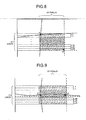
- FIGS. 8 and 9 are diagrams for explaining the line buffer 22 and the primary buffer of the pixel position conversion unit 41.
- the pixel position conversion unit 41 further includes a line buffer controller (an example of a line buffer control unit) 42 compared with the pixel position conversion unit 21 illustrated in FIG. 4 .
- the line buffer controller 42 forms a buffer memory control unit that determines lines to be stored in the line buffer 22 according to the position in the sub-scanning direction in the image data.
- the pixel position conversion unit 41 has a function to count the number of lines on the basis of the synchronizing signals such as Vsync_in, Hsync_in, and Href_in, and determines pixels in what lines to be stored in the line buffer 22 at what line in the image.
- the pixel of the point A illustrated in (c) of FIG. 2 is moved to the point A' located at +30 pixels in the X direction and -20 lines in the Y direction by the distortion of the image as described above.
- the pixel of the point C at the upper right end on the same line as the point A in the X direction is moved to the point C' located at -30 pixels in the X direction and -20 lines in the Y direction and the pixel of the point F on the Y axis on the same line is moved to the point F' moved by substantially zero pixel in the X direction and located at smaller than 20 lines in an absolute value in the minus direction in the Y direction.
- FIG. 9 illustrates an enlarged area around the point A illustrated in (c) of FIG. 2 .
- a total of 21 lines including a line in which the target pixel is included and 20 lines from the line in the minus direction are stored in the line buffer.
- L1 to L21 correspond to the above 21 lines.
- FIG. 9 illustrates the above situation (actually, the point G is a pixel above the X axis by a half pixel or a pixel below the X axis by a half pixel. In FIG. 9 , the point G is a pixel above the X axis by a half pixel.).
- the absolute value of the amount of movement is smaller than or equal to 30 pixels in the plus direction in the X direction and substantially zero in the Y direction.
- the amount of movement in the Y direction is not necessarily zero due to a manufacturing error and an individual difference of an actual lens and a relative position between the lens and the image capturing sensor.
- the amount of movement in the Y direction is unignorable in a camera device, which requires highly accurate distortion correction, such as a stereo camera device which performs a correlation calculation between images from a camera device including two or more image capturing elements and two or more optical systems. Therefore, the pixel position conversion unit 41 stores pixels of a total of 21 lines including a line in which the target pixel is included, 10 lines immediately above the line, and 10 lines immediately below the line into the line buffer. By doing so, it is possible to accurately perform the distortion correction even when the movement direction in the Y direction varies in the plus and minus directions in the same line.
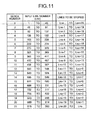
- FIGS. 10 and 11 illustrate correspondences between input lines and lines whose pixels are stored when an image is inputted from the image sensor 12.
- the input lines are divided into 20 blocks; in FIG. 11 , the input lines are divided into 21 blocks.
- an image of a total of 21 lines from the 940th line to the 960th line is required to output the 960th line.
- an area near the center of the image area near the 480th line
- the distortion in the sub-scanning direction is smaller than that in the ends of the image
- a distortion in the vertical direction may occur.
- the distortion can be sufficiently corrected if there is, for example, an image from the 471st line to the 491st line.
- the 960 line is equally divided into 20 blocks and lines to be stored in the line buffer are switched at the boundaries between the blocks.
- the lines to be stored are switched every 48 lines.
- lines from the (Lno)th line to the (Lno + 20)th line are stored in the line buffer. Specifically, at the first line, 21 lines from the first line to the 21st line are stored, and at the second line, 21 lines from the second line to the 22nd line are stored. Similarly, at the 48th line, 21 lines from the 48th line to the 68th line are stored.
- the next block is used, so that lines from the (Lno - 1)th line to the (Lno + 19)th line are stored in the line buffer.
- lines from the 48th line to the 68th line are stored. This is the same as the image data required to output the 48th line. Therefore, at the timing when the block is switched, the image stored in the line buffer does not change.
- 21 lines from the 49th line to the 69th line are stored. Thereafter, in the same manner as in the first block, lines are stored in the line buffer by shifting one line at a time.
- FIG. 10 illustrates an example in which the image is divided into 21 blocks. In this case, there is no operation in which two lines are shifted between the blocks.
- the total number of lines cannot be divided by the number of blocks, so that the fractional part of the number of input lines corresponding to each block needs to be rounded off, rounded down, or rounded up to set target input lines. Further, the number of input lines corresponding to each block varies, so that the switching timing between the blocks is somewhat complicated.
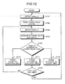
- FIG. 12 is a flowchart illustrating processing of the line buffer controller 42.
- the line buffer controller 42 includes a counter for counting the number of input lines.
- Step S101 When detecting an input of Vsync_in that indicates a head of one frame of an image (Step S101), the line buffer controller 42 resets a count value cnt of the counter to an initial value (here, 0) (Step S102).
- the line buffer controller 42 increments the count value of the counter by 1.
- the line buffer controller 42 checks the quotient of (count value -1)/48 (Step S105).
- the lines to be stored are switched every 48 input lines in each block. Therefore, it is possible to determine which block is currently processed by checking the quotient of (count value -1)/48. In practice, the quotient +1 is a block number.
- the line buffer controller 42 stores 21 lines from Lno to Lno + 20 in the line buffer 22 (Step S110).
- the quotient is 0 at the 48th line, so that it is possible to determine that the block number is block 1.
- the line buffer controller 42 stores 21 lines from Lno - 1 to Lno + 19 in the line buffer 22 (Step S111).
- the line buffer controller 42 selects 21 lines corresponding to each line and stored them in the line buffer.
- the line buffer controller 42 stores 21 lines of "Lno - 2 to Lno + 18" to "Lno -20 to Lno” in the line buffer 22 (Step S119) as illustrated in FIG. 10 .
- the line buffer controller 42 determines whether or not the input line is the last line (here, the 960th line) (Step S120).
- the line buffer controller 42 determines that the input line is not the last line and thus waits for an input of Hsync_in (Step S103) in order to input the next line.
- Step S120 Yes
- the line buffer controller 42 waits for an input of Vsync_in (Step S103) in order to input the next frame.
- the process after that is basically the same as the operation of the pixel position conversion unit 21.
- the capacity of the primary buffer can be small because the number of lines stored in the line buffer is smaller than that of the pixel position conversion unit 21.
- the primary buffer holds a total of 61 pixels in the horizontal direction including 30 pixels in the plus direction, 30 pixels in the minus direction, and a target pixel regarding the X direction and a total of 21 pixels in the vertical direction including 20 pixels in the minus direction and a target pixel regarding the Y direction.
- the primary buffer holds image data of 61 pixels ⁇ 21 lines of the image data stored in the line buffer.
- the primary buffer is actually formed by a flip-flop group or a memory resource (BRAM) or the like of a hardware macro when an FPGA or the like is used.
- BRAM memory resource
- the primary buffer is formed by the former, for example, if the bit depth of pixel is 12 bits, 61 ⁇ 21 flip-flops having a width of 12 bits are required, that is, 1,281 flip-flops are required. As a result, the number of flip-flops can be reduced to about half compared with a conventional technique.
- the interpolation process of the interpolator in the next stage is a bilinear method that requires 2 ⁇ 2 pixels, 2 ⁇ 21 BRAMs, that is, 42 BRAMs, are required. As a result, the number of BRAMs can be also reduced to about half compared with the pixel position conversion unit 21.
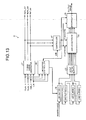
- FIG. 13 is a diagram for explaining a hardware configuration of a pixel position conversion unit 51 that can be applied to a camera device according to a second embodiment of the present invention.
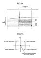
- FIG. 14 is a diagram for explaining a line buffer 22 and a primary buffer of the pixel position conversion unit 51.
- a controller 24 forms a distortion amount calculation unit that calculates the amount of distortion of image data for each pixel and the amount of distortion in the Y direction calculated by the controller 24 is inputted into a line buffer controller 52.
- the line buffer controller 52 controls in more detail the lines to be stored in the line buffer 22 than the first embodiment illustrated in FIG. 7 according to the direction of distortion and the amount of distortion in the Y direction calculated by the controller 24.
- the amount of movement of the point F in the Y direction is -5 lines
- the amount of movement in the Y direction on a line including the points A, C, and F is -5 to - 20 lines.
- the distortion can be corrected.
- the distortion can be corrected by the line buffer 22 of 16 lines.
- the line buffer controller 52 determines in more detail the lines to be stored in the line buffer 22 by using the direction of distortion (including the plus/minus directions) and the amount of distortion in the Y direction which are calculated by the controller 24, so that the memory resources of the line buffer 22 and the primary buffer can be reduced more than those in the first embodiment.
- the image capturing device since the image capturing device is configured as described above, the image capturing device includes a buffer memory control unit that determines a line to be stored in the buffer memory according to the position in the sub-scanning direction, so that it is possible to realize an accurate distortion correction using a small number of lines in the line buffer even when the plus/minus direction of the distortion varies in each quadrant or the plus/minus direction of the distortion varies in the sub-scanning direction on a certain line.
Landscapes
- Engineering & Computer Science (AREA)
- Multimedia (AREA)
- Signal Processing (AREA)
- Image Processing (AREA)
- Facsimile Scanning Arrangements (AREA)
- Image Input (AREA)
- Studio Devices (AREA)
- Cameras In General (AREA)
- Stereoscopic And Panoramic Photography (AREA)
Applications Claiming Priority (2)
| Application Number | Priority Date | Filing Date | Title |
|---|---|---|---|
| JP2012036080 | 2012-02-22 | ||
| JP2013008953A JP2013201753A (ja) | 2012-02-22 | 2013-01-22 | 撮像装置及び撮像方法 |
Publications (2)
| Publication Number | Publication Date |
|---|---|
| EP2632151A2 true EP2632151A2 (de) | 2013-08-28 |
| EP2632151A3 EP2632151A3 (de) | 2015-06-10 |
Family
ID=47912904
Family Applications (1)
| Application Number | Title | Priority Date | Filing Date |
|---|---|---|---|
| EP13156279.5A Withdrawn EP2632151A3 (de) | 2012-02-22 | 2013-02-22 | Bilderfassungsvorrichtung und Bilderfassungsverfahren |
Country Status (2)
| Country | Link |
|---|---|
| EP (1) | EP2632151A3 (de) |
| JP (1) | JP2013201753A (de) |
Cited By (1)
| Publication number | Priority date | Publication date | Assignee | Title |
|---|---|---|---|---|
| US11948225B2 (en) | 2020-09-18 | 2024-04-02 | Kabushiki Kaisha Toshiba | Image processing apparatus |
Citations (1)
| Publication number | Priority date | Publication date | Assignee | Title |
|---|---|---|---|---|
| JP2008236544A (ja) | 2007-03-22 | 2008-10-02 | Fujifilm Corp | 撮像装置および画像処理方法 |
Family Cites Families (5)
| Publication number | Priority date | Publication date | Assignee | Title |
|---|---|---|---|---|
| JP2004362069A (ja) * | 2003-06-02 | 2004-12-24 | Olympus Corp | 画像処理装置 |
| JP5553579B2 (ja) * | 2009-11-09 | 2014-07-16 | 三星電子株式会社 | デジタルカメラ、画像処理方法及びコンピュータプログラム |
| JP5607345B2 (ja) * | 2009-12-16 | 2014-10-15 | 三星電子株式会社 | 画像処理装置及び画像処理方法 |
| US8537244B2 (en) * | 2009-12-16 | 2013-09-17 | Samsung Electronics Co., Ltd. | Image processing apparatus and method, and computer-readable medium having stored thereon computer program for executing the method |
| JP2011205587A (ja) * | 2010-03-26 | 2011-10-13 | Olympus Corp | マルチバンドステレオ撮像装置 |
-
2013
- 2013-01-22 JP JP2013008953A patent/JP2013201753A/ja active Pending
- 2013-02-22 EP EP13156279.5A patent/EP2632151A3/de not_active Withdrawn
Patent Citations (1)
| Publication number | Priority date | Publication date | Assignee | Title |
|---|---|---|---|---|
| JP2008236544A (ja) | 2007-03-22 | 2008-10-02 | Fujifilm Corp | 撮像装置および画像処理方法 |
Cited By (1)
| Publication number | Priority date | Publication date | Assignee | Title |
|---|---|---|---|---|
| US11948225B2 (en) | 2020-09-18 | 2024-04-02 | Kabushiki Kaisha Toshiba | Image processing apparatus |
Also Published As
| Publication number | Publication date |
|---|---|
| JP2013201753A (ja) | 2013-10-03 |
| EP2632151A3 (de) | 2015-06-10 |
Similar Documents
| Publication | Publication Date | Title |
|---|---|---|
| KR101313686B1 (ko) | 화상처리장치 및 그 제어 방법 | |
| US10659746B2 (en) | Image processing device and image processing method | |
| JP2015049402A (ja) | 焦点ずれ量検出装置およびその制御方法、撮像装置 | |
| US20130120538A1 (en) | Stereo camera module | |
| JP2011061444A (ja) | 収差補正装置及び収差補正方法 | |
| JP4821704B2 (ja) | 画像歪み補正方法 | |
| JP6565326B2 (ja) | 撮像表示装置及びその制御方法 | |
| EP2632151A2 (de) | Bilderfassungsvorrichtung und Bilderfassungsverfahren | |
| JP6289243B2 (ja) | 像振れ補正装置及びその制御方法、プログラム、記憶媒体 | |
| JP2022181027A (ja) | 画像処理装置、画像処理方法、撮像装置、およびプログラム | |
| US7710469B2 (en) | Image acquisition apparatus | |
| JP5012875B2 (ja) | 高速動画像撮影装置、高速動画像撮影方法 | |
| US8780228B2 (en) | Image capture apparatus and control method thereof | |
| KR101854355B1 (ko) | 다중센서를 선택적으로 이용하는 영상보정 장치 | |
| US20030160885A1 (en) | AF evaluation value calculating device | |
| JP5351200B2 (ja) | 画像処理装置、画像処理システムおよび画像処理方法 | |
| JP2014219764A (ja) | 画像処理装置、画像処理方法およびプログラム | |
| JP2013190872A (ja) | 画像処理装置及び画像処理方法 | |
| JP2007079708A (ja) | 画像処理装置及び画像処理方法 | |
| JP2014154977A (ja) | 画像処理装置、画像処理方法、および撮像装置 | |
| KR101841744B1 (ko) | Cmos 이미지 센서를 집적한 스테레오 이미지 정합 시스템 및 방법 | |
| JP6649723B2 (ja) | 表示装置 | |
| JP6148568B2 (ja) | 固体撮像装置および映像信号補正プログラム | |
| JP5808197B2 (ja) | 映像処理装置及び映像処理方法 | |
| JP6091082B2 (ja) | 画像処理装置、画像処理方法、及び、プログラム |
Legal Events
| Date | Code | Title | Description |
|---|---|---|---|
| PUAI | Public reference made under article 153(3) epc to a published international application that has entered the european phase |
Free format text: ORIGINAL CODE: 0009012 |
|
| 17P | Request for examination filed |
Effective date: 20130222 |
|
| AK | Designated contracting states |
Kind code of ref document: A2 Designated state(s): AL AT BE BG CH CY CZ DE DK EE ES FI FR GB GR HR HU IE IS IT LI LT LU LV MC MK MT NL NO PL PT RO RS SE SI SK SM TR |
|
| AX | Request for extension of the european patent |
Extension state: BA ME |
|
| PUAL | Search report despatched |
Free format text: ORIGINAL CODE: 0009013 |
|
| AK | Designated contracting states |
Kind code of ref document: A3 Designated state(s): AL AT BE BG CH CY CZ DE DK EE ES FI FR GB GR HR HU IE IS IT LI LT LU LV MC MK MT NL NO PL PT RO RS SE SI SK SM TR |
|
| AX | Request for extension of the european patent |
Extension state: BA ME |
|
| RIC1 | Information provided on ipc code assigned before grant |
Ipc: H04N 5/357 20110101AFI20150507BHEP |
|
| 17Q | First examination report despatched |
Effective date: 20170220 |
|
| STAA | Information on the status of an ep patent application or granted ep patent |
Free format text: STATUS: THE APPLICATION IS DEEMED TO BE WITHDRAWN |
|
| 18D | Application deemed to be withdrawn |
Effective date: 20170704 |