EP2625724B1 - Optoelektronisches halbleiterbauelement und verfahren zu seiner herstellung - Google Patents
Optoelektronisches halbleiterbauelement und verfahren zu seiner herstellung Download PDFInfo
- Publication number
- EP2625724B1 EP2625724B1 EP11766989.5A EP11766989A EP2625724B1 EP 2625724 B1 EP2625724 B1 EP 2625724B1 EP 11766989 A EP11766989 A EP 11766989A EP 2625724 B1 EP2625724 B1 EP 2625724B1
- Authority
- EP
- European Patent Office
- Prior art keywords
- glass
- substrate
- phosphor
- semiconductor component
- optoelectronic semiconductor
- Prior art date
- Legal status (The legal status is an assumption and is not a legal conclusion. Google has not performed a legal analysis and makes no representation as to the accuracy of the status listed.)
- Active
Links
Images

Classifications
-
- H—ELECTRICITY
- H10—SEMICONDUCTOR DEVICES; ELECTRIC SOLID-STATE DEVICES NOT OTHERWISE PROVIDED FOR
- H10H—INORGANIC LIGHT-EMITTING SEMICONDUCTOR DEVICES HAVING POTENTIAL BARRIERS
- H10H20/00—Individual inorganic light-emitting semiconductor devices having potential barriers, e.g. light-emitting diodes [LED]
- H10H20/80—Constructional details
- H10H20/85—Packages
- H10H20/858—Means for heat extraction or cooling
- H10H20/8581—Means for heat extraction or cooling characterised by their material
-
- H—ELECTRICITY
- H10—SEMICONDUCTOR DEVICES; ELECTRIC SOLID-STATE DEVICES NOT OTHERWISE PROVIDED FOR
- H10H—INORGANIC LIGHT-EMITTING SEMICONDUCTOR DEVICES HAVING POTENTIAL BARRIERS
- H10H20/00—Individual inorganic light-emitting semiconductor devices having potential barriers, e.g. light-emitting diodes [LED]
- H10H20/80—Constructional details
- H10H20/85—Packages
-
- H—ELECTRICITY
- H10—SEMICONDUCTOR DEVICES; ELECTRIC SOLID-STATE DEVICES NOT OTHERWISE PROVIDED FOR
- H10H—INORGANIC LIGHT-EMITTING SEMICONDUCTOR DEVICES HAVING POTENTIAL BARRIERS
- H10H20/00—Individual inorganic light-emitting semiconductor devices having potential barriers, e.g. light-emitting diodes [LED]
- H10H20/80—Constructional details
- H10H20/85—Packages
- H10H20/851—Wavelength conversion means
-
- H—ELECTRICITY
- H10—SEMICONDUCTOR DEVICES; ELECTRIC SOLID-STATE DEVICES NOT OTHERWISE PROVIDED FOR
- H10H—INORGANIC LIGHT-EMITTING SEMICONDUCTOR DEVICES HAVING POTENTIAL BARRIERS
- H10H20/00—Individual inorganic light-emitting semiconductor devices having potential barriers, e.g. light-emitting diodes [LED]
- H10H20/80—Constructional details
- H10H20/85—Packages
- H10H20/851—Wavelength conversion means
- H10H20/8514—Wavelength conversion means characterised by their shape, e.g. plate or foil
-
- H—ELECTRICITY
- H10—SEMICONDUCTOR DEVICES; ELECTRIC SOLID-STATE DEVICES NOT OTHERWISE PROVIDED FOR
- H10H—INORGANIC LIGHT-EMITTING SEMICONDUCTOR DEVICES HAVING POTENTIAL BARRIERS
- H10H20/00—Individual inorganic light-emitting semiconductor devices having potential barriers, e.g. light-emitting diodes [LED]
- H10H20/80—Constructional details
- H10H20/85—Packages
- H10H20/851—Wavelength conversion means
- H10H20/8511—Wavelength conversion means characterised by their material, e.g. binder
-
- H—ELECTRICITY
- H10—SEMICONDUCTOR DEVICES; ELECTRIC SOLID-STATE DEVICES NOT OTHERWISE PROVIDED FOR
- H10H—INORGANIC LIGHT-EMITTING SEMICONDUCTOR DEVICES HAVING POTENTIAL BARRIERS
- H10H20/00—Individual inorganic light-emitting semiconductor devices having potential barriers, e.g. light-emitting diodes [LED]
- H10H20/80—Constructional details
- H10H20/85—Packages
- H10H20/858—Means for heat extraction or cooling
- H10H20/8583—Means for heat extraction or cooling not being in contact with the bodies
Definitions
- the invention is based on an optoelectronic semiconductor component according to the preamble of claim 1, in particular a conversion LED. It also describes an associated manufacturing method according to the preamble of claim 9.
- the US Pat. No. 5,998,925 discloses a typical white LED.
- the phosphor is suspended in silicone and then applied to the chip, usually it is screen printed.
- the layers are about 30 microns thick. Silicone has a poor thermal conductivity, which causes the phosphor to heat up more during operation and become inefficient.
- the conversion element is attached to the chip with an organic adhesive.
- the WO 2006/122524 describes a luminescence conversion LED using a phosphor embedded in glass.
- US 2009/001390 A1 (YAN XIANTAO [US] ET AL) describes a light emitting diode with Lumineszenzkonversions glass matrix.
- An object of the present invention is, in an optoelectronic semiconductor device according to the preamble of claim 1, an improved solution for the Specify problem of heat dissipation in the conversion element. Another object is to specify a manufacturing method for it.
- the present invention solves the following problem: improved efficiency and lifetime of the LED by increased heat dissipation of the conversion element by replacement of the organic material (plastic) by glass and ceramic or glass ceramic, which have better thermal conductivity and UV resistance.
- a modified approach of a separate conversion element which is structured is used: use of a thin transparent or translucent ceramic or glass ceramic foil as substrate or carrier material.
- the thickness of the carrier film is in the range of ⁇ 1 ⁇ m to ⁇ 100 ⁇ m, preferably ⁇ 3 ⁇ m to ⁇ 50 ⁇ m, in particular ⁇ 5 ⁇ m to ⁇ 20 ⁇ m.
- This film can, for. B. produced by doctor Blade method and then thermally sintered. Subsequently, a thin compact and relatively low-bubble glass layer is laminated to the film. The importance of a low-bubble layer lies in its reduced scattering effect.
- low-bubble means, in particular, that the proportion of bubbles in the glass layer is at most 10% by volume, preferably at most 5% by volume, particularly preferably at most 1% by volume. Due to the temperature control during production In the glass matrix, this parameter can be set specifically. The higher the temperature, the less bubbles the glass layer becomes. The sinking of the phosphor is carried out in comparison at significantly lower temperatures in order to avoid damage to the phosphor as possible.
- the thickness of the glass layer is ⁇ 200 ⁇ m, preferably ⁇ 100 ⁇ m, in particular ⁇ 50 ⁇ m, but at least as high as the largest phosphor particles.
- This layer can, for. B. by screen printing of glass powder with subsequent glazing or by applying molten glass are applied directly to the film.
- material for the substrate is preferably Al 2 O 3 , YAG, AlN, AlON, SiAlON or a glass ceramic.
- As a material for the glass layer is preferably a low-melting glass, preferably lead-free or lead poor, having a softening temperature ⁇ 500 ° C, preferably 350 to 480 ° C, such as in DE 10 2010 009 456.0 described.
- this system forms a laminate.
- a phosphor by z. B. screen printing or spraying applied to the glass layer of the laminate is then heated as far as possible (in particular, the temperature is at most at the so-called hemisphere point of the glass, in particular at least Tg of the glass, more preferably at least the softening temperature of the glass) that the glass softens only slightly and the phosphor sinks into the glass layer and is enclosed by it.
- the advantage of sinking is that only low temperatures are required and thus the phosphor is not damaged. In the case of the glass off DE 10 2010 009 456.0 this is a temperature of at most 350 ° C.
- Suitable luminescent substances are in principle all known phosphors suitable for LED conversion or mixtures of phosphors, in particular garnets, nitridosilicates, orthosilicates, sions, sialones, calsines, etc.
- Another example is the application of a powder mixture of glass powder and phosphor to the sintered film, the substrate.
- a powder mixture of glass powder and phosphor to the sintered film, the substrate.
- sinking in particular a temperature which corresponds at least to the pour point of the glass and preferably at most the refining temperature of the glass in order to produce a low-bubble layer, since the glass must be very low viscosity, so that the trapped air can escape and the phosphor particles also act to increase viscosity.
- B. vacuum during sintering necessary In the case of the glass off DE 10 2010 009 456.0 this would be at temperatures of at least 400 ° C.
- the substrate it is possible to choose the substrate as a very thin film of ceramic or glass ceramic and then to infiltrate with glass.
- the substrate in this case only slightly sintered, this is the Decreases sintering temperature compared to a "more compact" sintering or shortens the sintering time; that is, only chosen so high that the particles of the ceramic are fixed together and many pores remain, so a porous body is formed.
- the porosity is in the range between 30-70% by volume, preferably at least 50%.
- a thin, at least 1 .mu.m and at most 200 .mu.m thick glass layer is applied directly and then heated to a temperature which corresponds at least to the pour point of the glass, preferably at most the refining temperature of the glass, so that the glass is very thin and by capillary action into the porous film, which represents the substrate.
- the glass is preferably a low-melting glass, preferably lead-free or lead-poor, having a softening temperature of at most 500 ° C such as in DE 10 2010 009 456.0 described.
- the temperatures for infiltration in this case are at least 400 ° C, preferably at least 500 ° C.
- a glass excess can be selectively applied to the film so that a thin layer of glass remains on the surface of the film.
- the then applied to the substrate phosphor is allowed at relatively low temperatures of at least 50 ° C, preferably at higher temperatures, ie at a temperature which corresponds at most to the hemisphere point of the glass in the substrate, more precisely in the glass contained in the pores, sink.
- relatively low temperatures of at least 50 ° C, preferably at higher temperatures, ie at a temperature which corresponds at most to the hemisphere point of the glass in the substrate, more precisely in the glass contained in the pores, sink.
- this is a temperature of at most 350 ° C.
- the phosphor sinks into the surface structure of the glass-ceramic mixture of the substrate.
- the conversion element can be attached to the chip either with an inorganic adhesive such as a low melting glass or an inorganic sol-gel as well as with organic adhesive such as silicone or also an organic sol-gel. It can also be used as a "remote phosphor", ie away from the chip.
- an inorganic adhesive such as a low melting glass or an inorganic sol-gel as well as with organic adhesive such as silicone or also an organic sol-gel. It can also be used as a "remote phosphor", ie away from the chip.
- the glass used of the substrate, in particular of the laminate is low-melting and at the same time serves as an inorganic adhesive between the conversion element and the chip.
- a glass is for example in the DE 10 2010 009 456.0 described and allows sinking of the phosphor and a bonding of the chip and conversion element at temperatures ⁇ 350 ° C. The glass in this case faces the chip.
- the film may be coated on both sides with glass and possibly with phosphor on one or both sides.
- the application of the glass happens z. B. by immersion, so-called. Dipping, the film in the molten glass. Subsequently, the phosphor coating takes place and the sinking of the phosphor in the glass at low temperatures, possibly in two steps.
- the substrate in particular laminate, may also be a sandwich, i. H.
- the glass layer with the sunken phosphor is located between two foils, which are made of the same or different materials and are coated on one or both sides with glass.
- the glass material can be chosen differently.
- the glass is high refractive (preferably n> 1.8), in particular the refractive index of the glass is selected to be similar to the refractive index of the embedded phosphor component or components and similar to that of the ceramic / glass ceramic.
- the ceramic or glass ceramic foil may be facing or facing away from the chip.
- the ceramic also has a light-scattering effect.
- the latter depends u. a. from the grain size of the particles contained in the ceramic or glass ceramic and can sometimes be influenced by the temperature treatment.
- the particle size is typically ⁇ 60 ⁇ m, preferably ⁇ 40 ⁇ m, particularly preferably ⁇ 30 ⁇ m. It should be at least 1 nm, more preferably at least 5 nm, even better at least 10 nm, for many applications a minimum value of 100 nm is sufficient.
- a bundle of conversion elements in particular based on laminate, produced as a major part in one operation and only then cut into smaller parts, the actual conversion elements.
- the thickness of the glass layer with the sunken phosphor should preferably be ⁇ 200 ⁇ m, preferably ⁇ 100 ⁇ m, in particular ⁇ 50 ⁇ m.
- the thickness of the glass layer is at least as high as the largest phosphor particles of the phosphor powder used, in particular at least twice as thick.
- Suitable glass matrix are, for example, phosphate glasses and borate glasses, in particular alkali phosphate glasses, aluminum phosphate glasses, zinc phosphate glasses, phosphotellurite glasses, bismuth borate glasses, zinc borate glasses and zinc bismuth borate glasses.
- lead borate glasses are suitable in principle, they are not preferred because they are not RoHS compliant.
- the support film may consist of a ceramic such as Al 2 O 3 , YAG, AlN, AlON, SiAlON, etc., or a glass-ceramic.
- the thickness of the carrier film is preferably in the range ⁇ 100 ⁇ m, preferably ⁇ 50 ⁇ m, in particular ⁇ 20 ⁇ m. But it should be at least 1 micron, better 3 microns, preferably at least 5 microns thick.
- the crystals contained in the glass ceramic itself can be excited to fluorescence by exciting the primary emission of the chip and thus contribute to the conversion with.
- a well-known example is YAG: Ce.
- the ceramic film contains a phosphor such.
- B. YAG: Ce or it consists partially or completely of this.
- a thin low-bubble glass layer is laminated to the ceramic film, whereupon a separate phosphor is applied. This sinks by a subsequent slight warming in the glass.
- the applied separate phosphor can usually be another phosphor whose emission lies in a different spectral range than that of the yellow-emitting YAG: Ce.
- the separate phosphor is a red emitting phosphor which produces warm white light with a blue emitting chip and the yellow emitting ceramic. By choosing the proportion of the further phosphor, the color location of the LED can be controlled.
- an identical or similar phosphor as the phosphor already introduced in the ceramic of the substrate additionally in the glass layer is introduced, for example, to compensate for a chip-related Farbortschwankung (drift). It is also possible for a plurality of types of phosphor to be contained in the glassy layer of the conversion element. These do not necessarily have to be evenly distributed, they can also be introduced locally differently. Furthermore, oxidic particles such as Al 2 O 3 , TiO 2 , ZrO 2 may also be added to the phosphor as a scattering agent.
- two ceramics which already contain the phosphor are thinly coated with glass.
- the glassy layer of one of the two ceramic plates is then coated with phosphor, which sinks into this after a temperature treatment.
- Following the glassy surfaces of the two ceramic plates are placed on each other and glued together in a further temperature step.
- the color location of the two ceramic plates differs from that of the sunken phosphor.
- only one ceramic plate is thinly coated with glass and then glued at a temperature treatment with the other ceramic plate.
- the conversion element consists of a combination of glass and substrate, namely ceramic or glass ceramic, wherein a phosphor is embedded in glass.
- the glass matrix may u. U. simultaneously serve as an adhesive for the composite of chip and conversion element.
- the glass used should be chosen to be compact, i. melted and low in blisters.
- the substrate, whether ceramic or glass ceramic, can also serve as a light-scattering element and is at least translucent.
- the substrate, whether ceramic or glass ceramic can also contain or consist of phosphor itself.
- the optoelectronic semiconductor component may be an LED or else a laser.
- the invention relates to an optoelectronic semiconductor component according to the preamble of patent claim 1 and to a method for producing a conversion element for an optoelectronic semiconductor component according to the preamble of patent claim 9.
- FIG. 1 shows as a semiconductor device a conversion LED 1, which uses a chip 2 of the type InGaN as the primary radiation source. It has a housing 3 with a board 4, on which the chip sits, and a reflector 5. The chip is preceded by a conversion element 6, which partially converts the blue radiation by means of a phosphor, for example YAG: Ce, into longer-wave radiation.
- the conversion element 6 is platelet-shaped according to the prior art and has a silicone bed in which phosphor powder is dispersed. The electrical connections are not shown, they correspond to conventional technology.
- FIG. 2 shows a first non-inventive embodiment.
- a substrate 7 made of Al 2 O 3 is used as the conversion element 6, which is translucent and is shaped as a foil in the manner of a platelet.
- a thin glass layer 8 is applied, in the sense of a matrix. In this phosphor particles are distributed, which are sunk into the glass matrix and completely covered by this.
- Glass layer 8 and substrate 7 form a laminate, wherein the side of the substrate on which the glass matrix is applied, the chip 2 faces, or is also facing away.
- the conversion element is mounted by means of known adhesive on the chip (not shown).
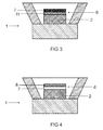
- FIG. 3 shows an inventive embodiment of an LED 1, in which the film of ceramic or glass ceramic, which acts as a substrate 7, is sintered only briefly at low temperature. That's why she has many open pores. The glass matrix fills these pores out. By using an excess of glass, a thin layer 11 of glass also remains on the surface of the substrate. The phosphor is dispersed in the glass matrix both in the region of the thin layer 11 and in the region of the pores.
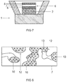
- FIG. 8 shows FIG. 8 in detail without layer 11. There, the substrate 7 is shown with open pores 12. Into the pores, the glass matrix 10 is sucked in. Phosphor grains 13 are dispersed in the glass matrix.
- FIG. 4 schematically shows a non-inventive embodiment of an LED 1, in which the substrate 7 via a conventional adhesive layer (not separately shown) with the chip 2 type InGaN blue (peak at about 440 to 450 nm) is connected.
- the glass matrix 8 with the phosphor immersed therein is fastened on the side of the substrate 7 facing away from the chip.
- the conventional adhesive layer is usually silicone. It is used when relatively temperature sensitive chips are used.
- an adhesive layer of high refractive index glass is more advantageous. Because then the heat dissipation is better and the light extraction is higher. This increases efficiency.
- an independent technical solution is to use the high refractive glasses presented alone as an adhesive (especially in the direction of the chip or the housing), that is without embedding a phosphor.
- the phosphor alone is introduced into the ceramic substrate or several phosphor-containing Ceramic substrates can be bonded together via such an adhesive.
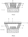
- FIG. 5 schematically shows a non-inventive embodiment of an LED 1, in which a double structure of the conversion element 6, 16 is used.
- a first layer 8 with glass matrix and first phosphor preferably a red-emitting phosphor such as a nitridosilicate M2Si5N8: Eu
- first substrate 7 which in turn is connected to a second glass matrix 8
- second Substrate 7 is connected.
- the glass matrix 8 acts in each case as an adhesive.
- Particularly suitable phosphors are YAG: Ce or another garnet, orthosilicate or sione, nitridosilicate, sialon, calsine, etc.
- FIG. 6 shows a non-inventive embodiment of an LED 1, which is a conversion element 6 spaced upstream of the chip 2.
- the side wall 5 of the housing which acts as a reflector, for example by the inner wall is suitably coated, at its end the conversion element 6.
- the glass matrix 8 acts as an adhesive to the side wall, the substrate 7 is remote from the chip.
- the conversion element 6 closes the opening of the reflector.
- FIG. 7 shows a non-inventive embodiment for an LED 1, in which a conversion element 6 sandwiched. It uses a UV emitting chip 2 with about 380 nm peak wavelength.
- a first glass matrix 8 adheres directly to the chip 2, in which a first phosphor is dispersed, for example a red, UV-excitable phosphor like the Calsin CaAlSiN3: Eu.
- a substrate 7 made of a mixture of YAG and YAG: Ce, which emits yellow.
- An additional blue emitting phosphor, such as BAM: Eu is dispersed in a second glass matrix 8, which is externally mounted in front of the substrate 7.
- Non-inventive embodiments of a converter for the conversion of the UV component into blue light are z.
- a non-inventive embodiment of a converter for the conversion of the UV component in yellow light is z.
- x and y are each in the range of 0.1 to 0.01.
- Non-inventive embodiments of a converter for the conversion of the UV component in red light are z.
Landscapes
- Led Device Packages (AREA)
Description
- Die Erfindung geht aus von einem optoelektronischen Halbleiterbauelement gemäß dem Oberbegriff des Anspruchs 1, insbesondere eine Konversions-LED. Sie beschreibt auch ein zugehöriges Herstellungsverfahren gemäß dem Oberbegriff des Anspruchs 9.
- Die
US 5 998 925 offenbart eine typische weiße LED. Dabei wird typisch der Leuchtstoff in Silikon suspendiert und dann auf den Chip aufgebracht, meist wird sie siebgedruckt. Die Schichten sind ca. 30 µm dick. Silikon besitzt eine schlechte Wärmeleitfähigkeit, die dazu führt, dass sich der Leuchtstoff im Betrieb stärker erwärmt und dadurch ineffizienter wird. Derzeit wird das Konversionselement mit einem organischen Kleber auf dem Chip befestigt. - Die
WO 2006/122524 beschreibt eine Lumineszenzkonversions-LED, die einen Leuchtstoff verwendet, der in Glas eingebettet ist. - Die
US 2009/001390 A1 (YAN XIANTAO [US] ET AL) beschreibt eine Leuchtdiode mit Lumineszenzkonversions-Glasmatrix. - Eine Aufgabe der vorliegenden Erfindung ist es, bei einem optoelektronisches Halbleiterbauelement gemäß dem Oberbegriff des Anspruchs 1 eine verbesserte Lösung für das Problem der Wärmeabfuhr beim Konversionselement anzugeben. Eine weitere Aufgabe ist es, dafür ein Herstellverfahren anzugeben.
- Diese Aufgabe wird gelöst durch die kennzeichnenden Merkmale der Ansprüche 1 und 9.
- Besonders vorteilhafte Ausgestaltungen finden sich in den abhängigen Ansprüchen.
- Die vorliegende Erfindung löst das folgende Problem: verbesserte Effizienz und Lebensdauer der LED durch stärkere Wärmeabfuhr des Konversionselements durch Ersatz des organischen Materials (Kunststoff) durch Glas und Keramik oder Glaskeramik, welche eine bessere Wärmeleitfähigkeit und UV-Beständigkeit besitzen.
- Beispielhaft wird ein modifizierter Ansatz eines separaten Konversionselements, das strukturiert ist, verwendet: Einsatz einer dünnen transparenten oder transluzenten Keramik- oder Glaskeramikfolie als Substrat oder Trägermaterial. Die Dicke der Trägerfolie liegt im Bereich ≥ 1 µm bis ≤ 100 µm, vorzugsweise ≥ 3 µm bis ≤ 50 µm, insbesondere ≥ 5 µm bis ≤ 20 µm. Diese Folie kann z. B. durch Doktor-Blade-Verfahren hergestellt und anschließend thermisch versintert werden. Im Anschluss wird auf die Folie eine dünne kompakte und relativ blasenarme Glasschicht laminiert. Die Bedeutung einer blasenarmen Schicht liegt in ihrer reduzierten Streuwirkung. Der Begriff blasenarm bedeutet insbesondere, dass der Anteil der Blasen in der Glasschicht höchstens 10 vol.-%, bevorzugt höchstens 5 vol.-%, besonders bevorzugt höchstens 1 vol.-% ausmacht. Durch die Temperaturführung bei der Herstellung der Glasmatrix kann dieser Parameter gezielt eingestellt werden. Je höher die Temperatur desto blasenärmer wird die Glasschicht. Das Einsinken des Leuchtstoffs wird im Vergleich dazu bei deutlich niedrigeren Temperaturen durchgeführt um eine Schädigung des Leuchtstoffs möglichst zu vermeiden.
- Je blasenärmer die Glasschicht, desto dünner kann die Glasschicht gewählt werden. Dies verbessert die Homogenität der Abstrahlung, also die Änderung des Farborts über den Winkel. Je geringer die Dicke der Glasschicht, desto mehr wird die unerwünschte seitliche Abstrahlung reduziert.
- Die Dicke der Glasschicht ist ≤ 200 µm, vorzugsweise ≤ 100 µm, insbesondere ≤ 50 µm, aber mindestens so hoch wie die größten Leuchtstoffpartikel. Diese Schicht kann z. B. durch Siebdruck von Glaspulver mit anschließender Verglasung oder durch Aufziehen von geschmolzenem Glas direkt auf die Folie aufgebracht werden. Als Material für das Substrat eignet sich bevorzugt Al2O3, YAG, AlN, AlON, SiAlON oder eine Glaskeramik. Als Material für die Glasschicht eignet sich bevorzugt ein niedrigschmelzendes Glas, vorzugsweise bleifrei oder bleiarm, mit einer Erweichungstemperatur < 500°C, bevorzugt 350 bis 480°C, wie beispielsweise in
DE 10 2010 009 456.0 beschrieben. Bevorzugt bildet dieses System ein Laminat. - Im Anschluss wird ein Leuchtstoff durch z. B. Siebdruck oder Sprühverfahren auf die Glasschicht des Laminats aufgebracht. Das mit Leuchtstoff beschichtete Laminat wird dann soweit erwärmt (insbesondere liegt dabei die Temperatur höchstens beim sog. Halbkugelpunkt des Glases, insbesondere bei mindestens Tg des Glases, besonders bevorzugt bei mindestens der Erweichungstemperatur des Glases), dass das Glas nur leicht erweicht und der Leuchtstoff in die Glasschicht einsinkt und davon umschlossen wird. Der Vorteil des Einsinkens ist, dass hierfür nur niedrige Temperaturen erforderlich sind und dadurch der Leuchtstoff nicht geschädigt wird. Im Falle des Glases aus
DE 10 2010 009 456.0 ist dies eine Temperatur von höchstens 350°C. Als Leuchtstoff eignen sich grundsätzlich alle bekannten für die LED-Konversion geeigneten Leuchtstoffe oder Mischungen von Leuchtstoffen wie insbesondere Granate, Nitridosilikate, Orthosilikate, Sione, Sialone, Calsine etc. - Ein weiteres Beispiel ist die Aufbringung einer Pulvermischung aus Glaspulver und Leuchtstoff auf die versinterte Folie, dem Substrat. Hierzu sind im Vergleich zum Einsinken aber deutlich höhere Temperaturen erforderlich, insbesondere eine Temperatur, die mindestens dem Fließpunkt des Glases und bevorzugt höchstens der Läutertemperatur des Glases entspricht, um eine blasenarme Schicht zu erzeugen, da dass Glas hierzu sehr niederviskos sein muss, so dass die eingeschlossene Luft entweichen kann und die Leuchtstoffpartikel außerdem viskositätserhöhend wirken. Eventuell sind Zusatzprozesse wie z. B. Vakuum während des Versinterns notwendig. Im Falle des Glases aus
DE 10 2010 009 456.0 wäre dies bei Temperaturen von mindestens 400°C. - Erfindungsgemäß ist es möglich, das Substrat als sehr dünne Folie aus Keramik oder Glaskeramik zu wählen und dann mit Glas zu infiltrieren. Im Vergleich zu beiden eingangs genannten Beispielen, muss das Substrat in diesem Fall nur leicht versintert werden, hierzu wird die Sintertemperatur gegenüber einem "kompakteren" Sintern erniedrigt oder die Sinterzeit verkürzt; d. h. nur so hoch gewählt, dass die Partikel der Keramik miteinander fixiert sind und viele Poren verbleiben, also ein poröser Körper entsteht. Die Porosität liegt im Bereich zwischen 30-70 Volumen-%, bevorzugt bei mindestens 50%. Im Anschluss wird eine dünne, mindestens 1 µm und höchstens 200 µm dicke Glasschicht direkt aufgebracht und dann auf eine Temperatur erwärmt, die mindestens dem Fließpunkt des Glases, bevorzugt höchstens der Läutertemperatur des Glases, entspricht, so dass das Glas sehr dünnflüssig wird und durch Kapillarwirkung in die poröse Folie, die das Substrat darstellt, gezogen wird. Dadurch wird das eigentliche Substrat gebildet. Bei dem Glas handelt es sich vorzugsweise um ein niedrigschmelzendes Glas, vorzugsweise bleifrei oder bleiarm, mit einer Erweichungstemperatur von höchstens 500°C wie beispielsweise in
DE 10 2010 009 456.0 beschrieben. Die Temperaturen zum Infiltrieren liegen in diesem Fall bei mindestens 400°C, vorzugsweise mindestens 500°C. - Dabei kann gezielt ein Glasüberschuss auf die Folie aufgebracht werden, damit auf der Oberfläche der Folie eine dünne Glasschicht verbleibt.
- Den dann auf das Substrat aufgebrachten Leuchtstoff lässt man bei relativ niedrigen Temperaturen von mindestens 50°C, bevorzugt bei höheren Temperaturen, d.h. bei einer Temperatur, die höchstens dem Halbkugelpunkt des Glases entspricht, in das Substrat, genauer in das in den Poren enthaltene Glas, einsinken. Im Falle des Glases aus
DE 10 2010 009 456.0 ist dies eine Temperatur von höchstens 350°C. - Bei einem Glasüberschuss verbleibt in einem ersten Ausführungsbeispiel auf der Oberfläche der Folie eine dünne Glasschicht, in die der Leuchtstoff einsinkt. In diesem Fall ist die Haftung wesentlich robuster als bei einem Laminat.
- Ist bei einem zweiten Ausführungsbeispiel ein Glasüberschuss an der Folienoberfläche nicht gegeben, sinkt der Leuchtstoff in die Oberflächenstruktur der Glas-Keramik-Mischung des Substrats ein.
- Das Konversionselement kann entweder mit einem anorganischen Kleber wie einem niedrigschmelzenden Glas oder einem anorganischen Sol-Gel als auch mit organischem Kleber wie Silikon oder auch einem organischen Sol-Gel auf dem Chip befestigt werden. Ebenfalls kann es als "remote phosphor", also mit Abstand zum Chip, eingesetzt werden.
- In einer besonderen Ausgestaltung ist das eingesetzte Glas des Substrats, insbesondere des Laminats, niedrigschmelzend und dient gleichzeitig als anorganischer Kleber zwischen Konversionselement und Chip. Ein derartiges Glas ist beispielsweise in der
DE 10 2010 009 456.0 beschrieben und ermöglicht ein Einsinken des Leuchtstoffs und ein Verkleben von Chip und Konversionselement bei Temperaturen ≤ 350°C. Das Glas ist in diesem Fall dem Chip zugewandt. - In einer weiteren Ausgestaltung kann die Folie beidseitig mit Glas und ggf. mit Leuchtstoff auf einer oder beiden Seiten beschichtet sein. Das Aufbringen des Glases geschieht z. B. durch Eintauchen, sog. Dippen, der Folie in die Glasschmelze. Anschließend erfolgt die Leuchtstoffbeschichtung sowie das Einsinken des Leuchtstoffs in das Glas bei niedrigen Temperaturen, ggf. in zwei Schritten.
- Das Substrat, insbesondere Laminat, kann auch ein Sandwich sein, d. h. die Glasschicht mit dem eingesunkenen Leuchtstoff befindet sich zwischen zwei Folien, die aus dem gleichen oder aus verschiedenen Materialien bestehen und ein- oder beidseitig mit Glas beschichtet sind. Das Glasmaterial kann dabei verschieden gewählt sein.
- Vorzugsweise ist das Glas hochbrechend (vorzugsweise n>1.8), insbesondere ist der Brechungsindex des Glases ähnlich dem Brechungsindex der eingebetteten Leuchtstoffkomponente oder der Leuchtstoffkomponenten und ähnlich dem der Keramik/Glaskeramik gewählt.
- Die Keramik- oder Glaskeramikfolie kann dem Chip zu- oder abgewandt sein. In letzterem Fall hat die Keramik auch eine lichtstreuende Wirkung. Letztere hängt u. a. von der Korngröße der in der Keramik oder Glaskeramik enthaltenen Partikel ab und kann mitunter durch die Temperaturbehandlung beeinflusst werden. Die Korngröße liegt typischerweise bei ≤ 60 µm, bevorzugt bei ≤ 40 µm, besonders bevorzug ≤ 30 µm. Sie sollte wenigstens 1 nm, besser wenigstens 5 nm, noch besser wenigstens 10 nm betragen, für viele Anwendungen ist ein Mindestwert von 100 nm ausreichend.
- Vorzugsweise wird ein Bündel von Konversionselementen, insbesondere auf Laminat-Basis, als größeres Teil in einem Arbeitsgang hergestellt und erst dann in kleinere Teile, den eigentlichen Konversionselementen, geschnitten.
- Die Dicke der Glasschicht mit dem eingesunkenen Leuchtstoff sollte bevorzugt ≤ 200 µm sein, vorzugsweise ≤ 100 µm, insbesondere ≤ 50 µm. Bevorzugt ist die Dicke der Glasschicht mindestens so hoch wie die größten Leuchtstoffpartikel des verwendeten Leuchtstoffpulvers, insbesondere mindestens doppelt so dick.
- Als Glasmatrix eignen sich beispielsweise Phosphatgläser und Boratgläser, insbesondere Alkaliphosphatgläser, Aluminiumphosphatgläser, Zinkphosphatgläser, Phospotelluritgläser, Bismuthboratgläser, Zinkboratgläser und Zink-Bismuth-Boratgläser.
- Darunter fallen Zusammensetzungen aus den Systemen:
R2O-ZnO-Al2O3-B2O3-P2O5 (R2O = Alkalioxid) ;
- R2O-TeO2-P2O5(R2O = Alkali- und/oder Silberoxid), auch in Verbindung mit ZnO und/oder Nb2O5 wie z.B. Ag2O-TeO2-P2O5 ZnO-Nb2O5;
- ZnO-Bi2O3-B2O3, auch in Verbindung mit SiO2 und/oder Alkali- und/oder Erdalkalioxid und/oder Al2O3 wie z.B. ZnO-Bi2O3-B2O3-SiO2 oder ZnO-Bi2O3-B2O3-BaO-SrO-SiO2;
- ZnO-B2O3, auch in Verbindung mit SiO2 und/oder Alkali- und/oder Erdalkalioxid und/oder Al2O3 wie z.B. ZnO-B2O3-SiO2;
- Bi2O3-B2O3, auch in Verbindung mit SiO2 und/oder Alkakli- und/oder Erdalkalioxid und/oder Al2O3 wie z.B. Bi2O3-B2O3-SiO2.
- Bleiboratgläser sind im Prinzip zwar geeignet, werden jedoch nicht bevorzugt, da sie nicht RoHS-konform sind.
- Die Trägerfolie kann aus einer Keramik wie z.B. Al2O3, YAG, AlN, AlON, SiAlON usw. oder einer Glaskeramik bestehen. Die Dicke der Trägerfolie liegt bevorzugt im Bereich ≤ 100 µm, vorzugsweise ≤ 50 µm, insbesondere ≤ 20 µm. Sie sollte aber mindestens 1 µm, besser 3 µm, bevorzugt mindestens 5 µm dick sein.
- In einer weiteren Ausführungsform können die in der Glaskeramik enthaltenen Kristalle selbst durch Anregung der primären Emission des Chips zur Fluoreszenz angeregt werden und so zur Konversion mit beitragen. Ein bekanntes Beispiel ist YAG:Ce.
- In einer besonders bevorzugten Ausgestaltung enthält die Keramikfolie einen Leuchtstoff wie z. B. YAG:Ce, bzw. sie besteht teilweise oder vollständig aus diesem. Im Anschluss wird auf die Keramikfolie eine dünne blasenarme Glasschicht laminiert, worauf ein separater Leuchtstoff aufgebracht wird. Dieser sinkt durch eine nachfolgende leichte Erwärmung in das Glas ein. Bei dem aufgebrachten separaten Leuchtstoff kann es sich in aller Regel um eine anderen Leuchtstoff handeln, dessen Emission in einem anderen Spektralbereich liegt als der des gelb emittierenden YAG:Ce. Z.B. ist der separate Leuchtstoff ein Rot emittierender Leuchtstoff, wodurch mit einem blau emittierenden Chip und der gelb emittierenden Keramik warmweißes Licht erzeugt wird. Durch Wahl des Anteil des weiteren Leuchtstoffs kann der Farbort der LED gesteuert werden.
- Auch ist es möglich, dass ein gleicher oder ähnlicher Leuchtstoff wie der in der Keramik des Substrats bereits eingebrachte Leuchtstoff zusätzlich in die Glasschicht eingebracht wird, um z.B. eine chipbedingte Farbortschwankung (Drift) auszugleichen. Es können auch mehrere Leuchtstoffsorten in der glasigen Schicht des Konversionselements enthalten sein. Diese müssen dabei nicht unbedingt gleichmäßig verteilt sein, sie können auch lokal verschieden eingebracht sein. Ferner können dem Leuchtstoff auch oxidische Partikel wie z.B. Al2O3, TiO2, ZrO2 als Streumittel zugesetzt sein.
- In einer weiteren Ausgestaltung werden zwei Keramiken, die den Leuchtstoff bereits beinhalten (Keramikkonverter), dünn mit Glas beschichtet. Die glasige Schicht eines der beiden Keramikplättchen wird dann mit Leuchtstoff beschichtet, der nach einer Temperaturbehandlung in diese einsinkt. Im Anschluss werden die glasigen Oberflächen der beiden Keramikplättchen aufeinander gelegt und in einem weiteren Temperaturschritt miteinander verklebt. In der Regel unterscheidet sich dabei der Farbort der beiden Keramikplättchen von dem des eingesunkenen Leuchtstoffes.
- In einer besonderen Ausgestaltung des Vorgängerbeispiels wird nur ein Keramikplättchen dünn mit Glas beschichtet und dann bei einer Temperaturbehandlung mit dem anderen Keramikplättchen verklebt.
- Ferner ist es möglich, die Keramikfolie als Substrat beidseitig dünn mit Glas zu beschichten, so dass auch beidseitig Leuchtstoff mit gleicher oder verschiedener Emission aufgebracht sein kann. Ähnliches ist auch mit einer Glaskeramik als Substrat möglich. Ausführungsformen, die aus Kombinationen der verschiedenen Varianten wie oben beschrieben bestehen, sind ebenfalls möglich.
- Wesentlich ist, daß das Konversionselement aus einer Kombination von Glas und Substrat, nämlich Keramik oder Glaskeramik, besteht, wobei ein Leuchtstoff in Glas eingebettet ist. Die Glasmatrix kann u. U. gleichzeitig als Kleber für den Verbund von Chip und Konversionselement dienen. Das verwendete Glas sollte kompakt gewählt sein, d.h. aufgeschmolzen und blasenarm. Das Substrat, ob Keramik oder Glaskeramik, kann auch als lichtstreuendes Element dienen und ist zumindest transluzent. Das Substrat, ob Keramik oder Glaskeramik, kann auch selbst Leuchtstoff enthalten oder aus diesem bestehen.
- Das optoelektronische Halbleiterbauelement kann eine LED oder auch ein Laser sein.
- Die Erfindung betrifft ein optoelektronisches Halbleiterbauelement nach dem Oberbegriff des Patentanspruchs 1 und ein Verfahren zur Herstellung eines Konversionselements für ein optoelektronisches Halbleiterbauelement nach dem Oberbegriff des Patentanspruchs 9.
- Im Folgenden soll die Erfindung anhand von mehreren Ausführungsbeispielen näher erläutert werden. Die Figuren zeigen:
- Figur 1
- eine Konversions-LED gemäß dem Stand der Technik;
- Figur 2
- eine LED mit neuartigem Konverterelement;
- Figur 3-7
- je ein weiteres Ausführungsbeispiel für eine LED mit neuartigem Konverterelement;
- Figur 8
- ein Substrat mit Poren und darin enthaltener Glasmatrix, die Leuchtstoffpartikel enthält.
-
Figur 1 zeigt als Halbleiterbauelement eine Konversions-LED 1, die als primäre Strahlungsquelle einen Chip 2 vom Typ InGaN verwendet. Sie hat ein Gehäuse 3 mit einem Board 4, auf dem der Chip sitzt, und einem Reflektor 5. Dem Chip ist ein Konversionselement 6 vorgeschaltet, das teilweise die blaue Strahlung mittels eines Leuchtstoffs, beispielweise YAG:Ce, in längerwellige Strahlung konvertiert. Das Konversionselement 6 ist gemäß dem Stand der Technik plättchenförmig und weist ein Silikonbett auf, in dem Leuchtstoffpulver dispergiert ist. Die elektrischen Anschlüsse sind nicht dargestellt, sie entsprechen üblicher Technik. -
Figur 2 zeigt ein erstes nicht-erfindungsgemäßes Ausführungsbeispiel. Dabei wird als Konversionselement 6 ein Substrat 7 aus Al2O3 verwendet, das transluzent ist und plättchenartig als Folie geformt ist. Auf das Substrat 7 ist eine dünne Glasschicht 8 aufgebracht, im Sinne einer Matrix. In dieser sind Leuchtstoffpartikel verteilt, die in die Glasmatrix eingesunken sind und von dieser vollständig bedeckt sind. Glasschicht 8 und Substrat 7 bilden ein Laminat, wobei die Seite des Substrats, auf der die Glasmatrix aufgetragen ist, dem Chip 2 zugewandt ist, oder auch abgewandt ist. Das Konversionselement ist mittels bekannter Kleber auf dem Chip angebracht (nicht dargestellt). -
Figur 3 zeigt ein erfindungsgemäßes Ausführungsbeispiel einer LED 1, bei der die Folie aus Keramik oder Glaskeramik, die als Substrat 7 wirkt, nur kurz bei niedriger Temperatur angesintert ist. Deshalb hat sie viele offenen Poren. Die Glasmatrix füllt diese Poren aus. Durch Verwendung eines Überschusses an Glas verbleibt außerdem eine dünne Schicht 11 aus Glas auf der Oberfläche des Substrats. Der Leuchtstoff ist in der Glasmatrix sowohl im Bereich der dünnen Schicht 11 als auch im Bereich der Poren dispergiert. Eine ähnliche Konfiguration zeigtFigur 8 im Detail ohne Schicht 11. Dort ist das Substrat 7 mit offenen Poren 12 gezeigt. In die Poren ist die Glasmatrix 10 eingesogen. In der Glasmatrix sind Leuchtstoffkörner 13 dispergiert. -
Figur 4 zeigt schematisch ein nichterfindungsgemäßes Ausführungsbeispiel einer LED 1, bei der das Substrat 7 über eine konventionelle Klebeschicht (nicht extra dargestellt) mit dem Chip 2 vom Typ InGaN, der blau emittiert (Peak bei etwa 440 bis 450 nm), verbunden ist. Die Glasmatrix 8 mit dem darin eingesunkenen Leuchtstoff ist auf der vom Chip abgewandten Seite des Substrats 7 befestigt. Die konventionelle Klebeschicht ist meist Silikon. Sie wird verwendet, wenn relativ temperaturempfindliche Chips verwendet werden. - Bei weniger temperaturempfindlichen Chips ist eine Klebeschicht aus hochbrechendem Glas vorteilhafter. Denn dann ist die Wärmeableitung besser und auch die Lichtauskopplung ist höher. Damit wird die Effizienz gesteigert.
- Aus diesem Grund ist eine eigenständige technische Lösung, die vorgestellten hochbrechenden Gläser allein als Kleber (insbesondere in Richtung zum Chip oder zum Gehäuse) zu verwenden, also ohne Einbettung eines Leuchtstoffs. In diesem Fall wird der Leuchtstoff allein in das keramische Substrat eingebracht bzw. mehrere Leuchtstoffhaltige keramische Substrate können über einen derartigen Kleber miteinander verbunden werden.
-
Figur 5 zeigt schematisch ein nicht-erfindungsgemäßes Ausführungsbeispiel einer LED 1, bei der eine doppelte Struktur des Konversionselements 6, 16 verwendet wird. Vom blau emittierenden Chip aus gesehen folgt auf eine erste Schicht 8 mit Glasmatrix und erstem Leuchtstoff, bevorzugt ein rot emittierender Leuchtstoff wie ein Nitridosilikat M2Si5N8:Eu, ein erstes Substrat 7, das wiederum mit einer zweiten Glasmatrix 8 verbunden ist, die wiederum mit einem zweiten Substrat 7 verbunden ist. Dabei wirkt die Glasmatrix 8 jeweils selbst als Kleber. - Geeignete Leuchtstoffe sind insbesondere YAG:Ce oder ein anderer Granat, Orthosilikat oder Sion, Nitridosilikat, Sialon, Calsin, etc..
-
Figur 6 zeigt ein nicht-erfindungsgemäßes Ausführungsbeispiel für eine LED 1, der ein Konversionselement 6 beabstandet vor den Chip 2 vorgeschaltet ist. Dabei trägt die Seitenwand 5 des Gehäuses, die als Reflektor wirkt, indem beispielsweise die Innenwand geeignet beschichtet ist, an ihrem Ende das Konversionselement 6. Wieder wirkt die Glasmatrix 8 auch als Kleber zur Seitenwand hin, das Substrat 7 ist vom Chip abgewandt. Das Konversionselement 6 verschließt die Öffnung des Reflektors. -
Figur 7 zeigt ein nicht-erfindungsgemäßes Ausführungsbeispiel für eine LED 1, bei der ein Konversionselement 6 sandwichartig aufgebaut. Es verwendet einen UV-emittierenden Chip 2 mit etwa 380 nm Peakwellenlänge. Eine erste Glasmatrix 8 klebt direkt auf dem Chip 2, in ihr ist ein erster Leuchtstoff dispergiert, beispielsweise ein roter, UV-anregbarer Leuchtstoff wie das Calsin CaAlSiN3:Eu. Vor der ersten Glasmatrix sitzt ein Substrat 7 aus einer Mischung von YAG und YAG:Ce, das gelb emittiert. Ein zusätzlicher blau emittierender Leuchtstoff wie BAM:Eu ist in einer zweiten Glasmatrix 8 dispergiert, die außen vor dem Substrat 7 angebracht ist. - Nicht-erfindungsgemäße Ausführungsbeispiele eines Konverters für die Konversion des UV-Anteils in blaues Licht sind z. B. hocheffiziente Leuchtstoffe vom Typ (Ba0.4Eu0.6) MgAl10O17, (Sr0,96Eu0,04)10 (PO4)6Cl2. Ein nicht-erfindungsgemäßes Ausführungsbeispiel eines Konverters für die Konversion des UV-Anteils in gelbes Licht ist z. B. (Sr1-x-yCexLiy)2Si5N8. Insbesondere liegt hier x und y jeweils im Bereich 0,1 bis 0,01. Besonders geeignet ist ein Leuchtstoff (Sr1-x-yCexLiy)2Si5N8, bei dem x=y. Nicht-erfindungsgemäße Ausführungsbeispiele eines Konverters für die Konversion des UV-Anteils in rotes Licht sind z. B. Nitridosilikate, Calsine oder Sione des Typs MSi2O2N2:Eu, die für sich genommen gut bekannt sind.
Claims (12)
- Optoelektronisches Halbleiterbauelement (1) mit einer Lichtquelle, einem Gehäuse und elektrischen Anschlüssen, wobei die Lichtquelle einen Chip (2) aufweist, der primäre Strahlung im UV oder Blauen emittiert, deren Peakwellenlänge insbesondere im Bereich 300 bis 490 nm liegt, wobei die primäre Strahlung teilweise oder vollständig durch ein davor angebrachtes Konversionselement in Strahlung anderer Wellenlänge umgewandelt wird, dadurch gekennzeichnet, dass das Konversionselement ein transluzentes oder transparentes Substrat (7) aufweist, das aus Keramik oder Glaskeramik gefertigt ist, wobei das Substrat mit einer Glasmatrix (10) beaufschlagt ist, in die ein Leuchtstoff (13) eingebettet ist, wobei das Substrat Poren (12) aufweist, in die die Glasmatrix zumindest teilweise eingebracht ist.
- Optoelektronisches Halbleiterbauelement nach Anspruch 1, dadurch gekennzeichnet, dass die Glasmatrix auf dem Substrat als Schicht aufgebracht ist.
- Optoelektronisches Halbleiterbauelement nach Anspruch 1, dadurch gekennzeichnet, dass das Substrat und die Glasmatrix ein Laminat bilden.
- Optoelektronisches Halbleiterbauelement nach Anspruch 1, dadurch gekennzeichnet, dass die Glasmatrix gleichzeitig als Kleber für einen Verbund von Chip und Konversionselement oder für einen Verbund zweier Konversionselemente dient.
- Optoelektronisches Halbleiterbauelement nach Anspruch 1, dadurch gekennzeichnet, dass die Glasmatrix blasenarm oder im wesentlichen frei von Blasen ist.
- Optoelektronisches Halbleiterbauelement nach Anspruch 1, dadurch gekennzeichnet, dass das Substrat selbst teilweise oder vollständig fluoreszierend ist.
- Optoelektronisches Halbleiterbauelement nach Anspruch 1, dadurch gekennzeichnet, dass das Substrat auf beiden Seiten mit einer Glasmatrix beaufschlagt ist.
- Optoelektronisches Halbleiterbauelement nach Anspruch 1, dadurch gekennzeichnet, dass das Konversionselement mittels eines Klebers auf dem Chip befestigt ist oder beabstandet vom Chip angebracht ist.
- Verfahren zur Herstellung eines Konversionselements für ein optoelektronisches Halbleiterbauelement (1) nach einem der vorhergehenden Ansprüche, dadurch gekennzeichnet, dass in einem ersten Schritt ein Substrat (7) bereitgestellt wird, das aus Keramik oder Glaskeramik hergestellt ist, dann in einem zweiten Schritt Glas auf das Substrat aufgetragen wird, insbesondere als Glaspulver oder geschmolzenes Glas, wobei entweder Leuchtstoff zusammen mit dem Glas aufgetragen wird, oder Leuchtstoff nachträglich in das Glas eingebracht wird, wobei im zweiten Schritt eine Glasmatrix (10) durch Infiltrieren erzeugt wird, wobei das Substrat vorher so gesintert worden ist, dass es große Poren (12) enthält, wobei das Glas so ausreichend dünnflüssig gemacht wird, dass es durch Kapillarwirkung in die Poren des Substrats hineingezogen wird.
- Verfahren nach Anspruch 9, dadurch gekennzeichnet, dass im zweiten Schritt eine Glasschicht laminiert wird, insbesondere entweder durch Siebdrucken von glasigem Pulver mit anschließender Verglasung oder durch Aufziehen von geschmolzenem Glas direkt auf das Substrat.
- Verfahren nach Anspruch 10, dadurch gekennzeichnet, dass der Leuchtstoff anschließend durch Siebdrucken oder ein Sprühverfahren auf die Glasschicht aufgebracht wird und dann das Konversionselement soweit erwärmt wird, dass das Glas leicht erwärmt wird, so dass der Leuchtstoff in das Glas einsinkt und davon umschlossen wird.
- Verfahren nach Anspruch 9, dadurch gekennzeichnet, dass im zweiten Schritt eine Glasschicht laminiert wird, die bereits mit Leuchtstoff versehen ist, insbesondere durch Siebdrucken von glasigem Pulver, das mit Leuchtstoffpulver vorher vermischt worden ist, mit anschließender Verglasung.
Applications Claiming Priority (2)
| Application Number | Priority Date | Filing Date | Title |
|---|---|---|---|
| DE102010042217A DE102010042217A1 (de) | 2010-10-08 | 2010-10-08 | Optoelektronisches Halbleiterbauelement und Verfahren zu seiner Herstellung |
| PCT/EP2011/067381 WO2012045772A1 (de) | 2010-10-08 | 2011-10-05 | Optoelektronisches halbleiterbauelement und verfahren zu seiner herstellung |
Publications (2)
| Publication Number | Publication Date |
|---|---|
| EP2625724A1 EP2625724A1 (de) | 2013-08-14 |
| EP2625724B1 true EP2625724B1 (de) | 2016-11-30 |
Family
ID=44764153
Family Applications (1)
| Application Number | Title | Priority Date | Filing Date |
|---|---|---|---|
| EP11766989.5A Active EP2625724B1 (de) | 2010-10-08 | 2011-10-05 | Optoelektronisches halbleiterbauelement und verfahren zu seiner herstellung |
Country Status (7)
| Country | Link |
|---|---|
| US (1) | US20130207151A1 (de) |
| EP (1) | EP2625724B1 (de) |
| JP (2) | JP2013539238A (de) |
| KR (1) | KR101845840B1 (de) |
| CN (1) | CN103155187B (de) |
| DE (1) | DE102010042217A1 (de) |
| WO (1) | WO2012045772A1 (de) |
Families Citing this family (21)
| Publication number | Priority date | Publication date | Assignee | Title |
|---|---|---|---|---|
| WO2013161683A1 (ja) | 2012-04-24 | 2013-10-31 | 株式会社光波 | 蛍光体及びその製造方法、並びに発光装置 |
| DE102012210083A1 (de) * | 2012-06-15 | 2013-12-19 | Osram Gmbh | Optoelektronisches halbleiterbauelement |
| KR101964418B1 (ko) * | 2012-07-02 | 2019-04-01 | 엘지이노텍 주식회사 | 형광체 조성물 및 이를 포함하는 조명 장치 |
| DE102012107290A1 (de) * | 2012-08-08 | 2014-02-13 | Osram Opto Semiconductors Gmbh | Optoelektronisches Halbleiterbauteil, Konversionsmittelplättchen und Verfahren zur Herstellung eines Konversionsmittelplättchens |
| DE102012107797A1 (de) * | 2012-08-23 | 2014-02-27 | Osram Opto Semiconductors Gmbh | Verfahren zur Herstellung eines Licht emittierenden Halbleiterbauelements und Licht emittierendes Halbleiterbauelement |
| DE102012108160A1 (de) * | 2012-09-03 | 2014-03-06 | Osram Opto Semiconductors Gmbh | Optoelektronisches Halbleiterbauelement und Verfahren zur Herstellung eines optoelektronischen Halbleiterbauelements |
| DE102012110668A1 (de) * | 2012-11-07 | 2014-05-08 | Osram Opto Semiconductors Gmbh | Konvertermaterial, Verfahren zur Herstellung eines Konvertermaterials und optoelektronisches Bauelement |
| DE102012220980A1 (de) | 2012-11-16 | 2014-05-22 | Osram Gmbh | Optoelektronisches halbleiterbauelement |
| CN111509112B (zh) * | 2013-07-08 | 2024-04-02 | 亮锐控股有限公司 | 波长转换的半导体发光器件 |
| CN103489857B (zh) * | 2013-09-06 | 2017-06-06 | 中山市天健照明电器有限公司 | 一种白光led发光装置 |
| KR102323289B1 (ko) * | 2014-01-07 | 2021-11-08 | 루미리즈 홀딩 비.브이. | 인광체 변환기를 갖는 비접착식 발광 디바이스 |
| JP2015142046A (ja) * | 2014-01-29 | 2015-08-03 | シャープ株式会社 | 波長変換部材、発光装置、および波長変換部材の製造方法 |
| JP6252982B2 (ja) * | 2014-02-06 | 2017-12-27 | 日本電気硝子株式会社 | ガラス部材及びその製造方法 |
| JP6575923B2 (ja) * | 2014-09-26 | 2019-09-18 | 日本電気硝子株式会社 | 波長変換部材及びそれを用いた発光装置 |
| JP2017188592A (ja) | 2016-04-06 | 2017-10-12 | 日亜化学工業株式会社 | 発光装置 |
| DE102017104134A1 (de) * | 2017-02-28 | 2018-08-30 | Osram Gmbh | Optoelektronisches Bauelement und Verfahren zur Herstellung eines optoelektronischen Bauelements |
| KR102462030B1 (ko) * | 2018-06-14 | 2022-11-01 | 인테벡, 인코포레이티드 | 멀티 칼라 절연 코팅 및 uv 잉크젯 프린팅 |
| US10475968B1 (en) | 2018-07-19 | 2019-11-12 | Osram Opto Semiconductors Gmbh | Optoelectronic component and a method for producing an optoelectronic component |
| EP3608959B1 (de) * | 2018-08-06 | 2023-11-15 | Nichia Corporation | Lichtemittierende vorrichtung und verfahren zu deren herstellung |
| JP6963720B2 (ja) | 2018-08-30 | 2021-11-10 | 日亜化学工業株式会社 | 発光装置 |
| WO2023072867A1 (en) * | 2021-10-29 | 2023-05-04 | Ams-Osram International Gmbh | Optoelectronic semiconductor chip, optoelectronic component and method for producing an optoelectronic semiconductor chip |
Family Cites Families (18)
| Publication number | Priority date | Publication date | Assignee | Title |
|---|---|---|---|---|
| TW383508B (en) | 1996-07-29 | 2000-03-01 | Nichia Kagaku Kogyo Kk | Light emitting device and display |
| US20030102473A1 (en) * | 2001-08-15 | 2003-06-05 | Motorola, Inc. | Structure and method for fabricating semiconductor structures and devices utilizing the formation of a compliant substrate |
| DE102004019802B4 (de) * | 2004-03-11 | 2007-01-25 | Schott Ag | Verwendung eines lumineszierenden Glases als Konversionsmedium zur Erzeugung von weißem Licht |
| US7553683B2 (en) * | 2004-06-09 | 2009-06-30 | Philips Lumiled Lighting Co., Llc | Method of forming pre-fabricated wavelength converting elements for semiconductor light emitting devices |
| US8324641B2 (en) * | 2007-06-29 | 2012-12-04 | Ledengin, Inc. | Matrix material including an embedded dispersion of beads for a light-emitting device |
| US8134292B2 (en) * | 2004-10-29 | 2012-03-13 | Ledengin, Inc. | Light emitting device with a thermal insulating and refractive index matching material |
| DE102005023134A1 (de) | 2005-05-19 | 2006-11-23 | Patent-Treuhand-Gesellschaft für elektrische Glühlampen mbH | Lumineszenzkonversions-LED |
| JP4765525B2 (ja) * | 2005-06-29 | 2011-09-07 | 日本電気硝子株式会社 | 発光色変換部材 |
| JP2007048864A (ja) * | 2005-08-09 | 2007-02-22 | Nippon Electric Glass Co Ltd | 蛍光体複合材料 |
| JP2007191702A (ja) * | 2005-12-22 | 2007-08-02 | Nippon Electric Glass Co Ltd | 発光色変換材料 |
| JP4969119B2 (ja) * | 2006-03-20 | 2012-07-04 | 日本碍子株式会社 | 発光ダイオード装置 |
| US8481977B2 (en) * | 2006-03-24 | 2013-07-09 | Goldeneye, Inc. | LED light source with thermally conductive luminescent matrix |
| JP4978886B2 (ja) * | 2006-06-14 | 2012-07-18 | 日本電気硝子株式会社 | 蛍光体複合材料及び蛍光体複合部材 |
| US20080121911A1 (en) * | 2006-11-28 | 2008-05-29 | Cree, Inc. | Optical preforms for solid state light emitting dice, and methods and systems for fabricating and assembling same |
| DE102007057812A1 (de) * | 2007-11-30 | 2009-06-25 | Schott Ag | Lichtemittierende Vorrichtung und Verfahren zu deren Herstellung sowie Lichtkonverter und dessen Verwendung |
| US8158247B2 (en) * | 2008-01-30 | 2012-04-17 | Los Alamos National Security, Llc | Porous light-emitting compositions |
| DE102008021666A1 (de) * | 2008-04-30 | 2009-11-05 | Ledon Lighting Jennersdorf Gmbh | Lichtemittierende Vorrichtung und Verfahren zur Herstellung einer lichtemittierenden Vorrichtung |
| DE102010009456A1 (de) | 2010-02-26 | 2011-09-01 | Osram Opto Semiconductors Gmbh | Strahlungsemittierendes Bauelement mit einem Halbleiterchip und einem Konversionselement und Verfahren zu dessen Herstellung |
-
2010
- 2010-10-08 DE DE102010042217A patent/DE102010042217A1/de not_active Withdrawn
-
2011
- 2011-10-05 WO PCT/EP2011/067381 patent/WO2012045772A1/de not_active Ceased
- 2011-10-05 US US13/878,249 patent/US20130207151A1/en not_active Abandoned
- 2011-10-05 CN CN201180048562.8A patent/CN103155187B/zh active Active
- 2011-10-05 EP EP11766989.5A patent/EP2625724B1/de active Active
- 2011-10-05 KR KR1020137011927A patent/KR101845840B1/ko active Active
- 2011-10-05 JP JP2013532182A patent/JP2013539238A/ja active Pending
-
2015
- 2015-03-10 JP JP2015047523A patent/JP6009020B2/ja not_active Expired - Fee Related
Also Published As
| Publication number | Publication date |
|---|---|
| CN103155187A (zh) | 2013-06-12 |
| DE102010042217A1 (de) | 2012-04-12 |
| JP2013539238A (ja) | 2013-10-17 |
| EP2625724A1 (de) | 2013-08-14 |
| KR20130114671A (ko) | 2013-10-17 |
| KR101845840B1 (ko) | 2018-04-06 |
| CN103155187B (zh) | 2016-12-07 |
| WO2012045772A1 (de) | 2012-04-12 |
| JP6009020B2 (ja) | 2016-10-19 |
| JP2015109483A (ja) | 2015-06-11 |
| US20130207151A1 (en) | 2013-08-15 |
Similar Documents
| Publication | Publication Date | Title |
|---|---|---|
| EP2625724A1 (de) | Optoelektronisches halbleiterbauelement und verfahren zu seiner herstellung | |
| DE10349038B4 (de) | Lichtquelle mit einer LED und einem Lumineszenzkonversionskörper und Verfahren zum Herstellen des Lumineszenzkonversionskörpers | |
| EP1501909B1 (de) | Wellenlängenkonvertierende reaktionsharzmasse und leuchtdiodenbauelement | |
| DE112015001180T5 (de) | Wellenlängenkonversionselement, lichtemittierende Halbleiterkomponente, die ein Wellenlängenkonversionselement umfasst, Verfahren zum Herstellen eines Wellenlängenkonversionselements und Verfahren zum Herstellen einer lichtemittierenden Halbleiterkomponente, die ein Wellenlängenkonversionselement umfasst | |
| WO2011104364A1 (de) | Strahlungsemittierendes bauelement mit einem halbleiterchip und einem konversionselement und verfahren zu dessen herstellung | |
| WO2013186365A1 (de) | Optoelektronisches halbleiterbauelement | |
| DE102013207308B4 (de) | Verfahren zum Herstellen einer optoelektronischen Baugruppe und optoelektronische Baugruppe | |
| DE112014005897B4 (de) | Konversionselement, Bauelement und Verfahren zur Herstellung eines Bauelements | |
| DE202009019173U1 (de) | Lichtemittierende Vorrichtung sowie Harzgehäuse und Harzformkörper | |
| WO2019179769A1 (de) | Optoelektronisches bauelement und verfahren zur herstellung eines optoelektronischen bauelements | |
| DE102012220980A1 (de) | Optoelektronisches halbleiterbauelement | |
| DE102011078689A1 (de) | Verfahren zur Herstellung eines Konversionselements und Konversionselement | |
| DE102013212247B4 (de) | Optoelektronisches Bauelement und Verfahren zu seiner Herstellung | |
| DE102018106655A1 (de) | Licht-emittierende Vorrichtung und Verfahren zu ihrer Herstellung | |
| DE102018123681A1 (de) | Trägersubstrat für elektrische, insbesondere elektronische Bauteile und Verfahren zum Herstellen eines Trägersubstrats | |
| DE112020005122T5 (de) | Leuchtstoffplatte, lichtemittierende Vorrichtung und Verfahren zur Herstellung einer Leuchtstoffplatte | |
| WO2024208667A1 (de) | Verfahren zur herstellung eines optoelektronischen bauelements und optoelektronisches bauelement | |
| DE102009010468A1 (de) | Strahlungsemittierendes Funktionsmaterial mit darauf angeordneten Lichtkonversionsstoff-Partikeln, Verfahren zu dessen Herstellung und optoelektronisches Bauelement, enthaltend ein derartiges Funktionsmaterial | |
| WO2011009737A1 (de) | Leuchtdiode mit einer keramischen abdeckung und verfahren zur herstellung dieser leuchtdiode | |
| DE112019003634T5 (de) | Optoelektronisches bauelement und das verfahren zur herstellung eines optoeklektronischen bauelements | |
| DE102018130526B4 (de) | Bauteil mit einem reflektierenden Gehäuse und Herstellungsverfahren für ein solches Bauteil | |
| WO2015107211A1 (de) | Verfahren zur herstellung einer lateral strukturierten phosphorschicht und optoelektronisches halbleiterbauteil mit einer solchen phosphorschicht | |
| DE102005012953B9 (de) | Verfahren zur Herstellung eines optoelektronischen Bauelements und optoelektronisches Bauelement | |
| WO2014191257A1 (de) | Anorganisches optisches element und verfahren zur herstellung eines anorganischen optischen elements | |
| DE102022132657A1 (de) | Lichtemittierende vorrichtung |
Legal Events
| Date | Code | Title | Description |
|---|---|---|---|
| PUAI | Public reference made under article 153(3) epc to a published international application that has entered the european phase |
Free format text: ORIGINAL CODE: 0009012 |
|
| 17P | Request for examination filed |
Effective date: 20130508 |
|
| AK | Designated contracting states |
Kind code of ref document: A1 Designated state(s): AL AT BE BG CH CY CZ DE DK EE ES FI FR GB GR HR HU IE IS IT LI LT LU LV MC MK MT NL NO PL PT RO RS SE SI SK SM TR |
|
| DAX | Request for extension of the european patent (deleted) | ||
| GRAP | Despatch of communication of intention to grant a patent |
Free format text: ORIGINAL CODE: EPIDOSNIGR1 |
|
| INTG | Intention to grant announced |
Effective date: 20160624 |
|
| RIC1 | Information provided on ipc code assigned before grant |
Ipc: H01L 33/50 20100101AFI20160614BHEP Ipc: H01L 33/64 20100101ALN20160614BHEP |
|
| GRAS | Grant fee paid |
Free format text: ORIGINAL CODE: EPIDOSNIGR3 |
|
| GRAA | (expected) grant |
Free format text: ORIGINAL CODE: 0009210 |
|
| AK | Designated contracting states |
Kind code of ref document: B1 Designated state(s): AL AT BE BG CH CY CZ DE DK EE ES FI FR GB GR HR HU IE IS IT LI LT LU LV MC MK MT NL NO PL PT RO RS SE SI SK SM TR |
|
| REG | Reference to a national code |
Ref country code: CH Ref legal event code: EP Ref country code: GB Ref legal event code: FG4D Free format text: NOT ENGLISH |
|
| REG | Reference to a national code |
Ref country code: AT Ref legal event code: REF Ref document number: 850551 Country of ref document: AT Kind code of ref document: T Effective date: 20161215 |
|
| REG | Reference to a national code |
Ref country code: IE Ref legal event code: FG4D Free format text: LANGUAGE OF EP DOCUMENT: GERMAN |
|
| RIN2 | Information on inventor provided after grant (corrected) |
Inventor name: KOTTER, STEFAN Inventor name: EBERHARDT, ANGELA Inventor name: SCHMIDT, REINHOLD Inventor name: HUETTINGER, ROLAND |
|
| REG | Reference to a national code |
Ref country code: DE Ref legal event code: R096 Ref document number: 502011011259 Country of ref document: DE |
|
| PG25 | Lapsed in a contracting state [announced via postgrant information from national office to epo] |
Ref country code: LV Free format text: LAPSE BECAUSE OF FAILURE TO SUBMIT A TRANSLATION OF THE DESCRIPTION OR TO PAY THE FEE WITHIN THE PRESCRIBED TIME-LIMIT Effective date: 20161130 |
|
| REG | Reference to a national code |
Ref country code: LT Ref legal event code: MG4D |
|
| PG25 | Lapsed in a contracting state [announced via postgrant information from national office to epo] |
Ref country code: GR Free format text: LAPSE BECAUSE OF FAILURE TO SUBMIT A TRANSLATION OF THE DESCRIPTION OR TO PAY THE FEE WITHIN THE PRESCRIBED TIME-LIMIT Effective date: 20170301 Ref country code: SE Free format text: LAPSE BECAUSE OF FAILURE TO SUBMIT A TRANSLATION OF THE DESCRIPTION OR TO PAY THE FEE WITHIN THE PRESCRIBED TIME-LIMIT Effective date: 20161130 Ref country code: NO Free format text: LAPSE BECAUSE OF FAILURE TO SUBMIT A TRANSLATION OF THE DESCRIPTION OR TO PAY THE FEE WITHIN THE PRESCRIBED TIME-LIMIT Effective date: 20170228 Ref country code: LT Free format text: LAPSE BECAUSE OF FAILURE TO SUBMIT A TRANSLATION OF THE DESCRIPTION OR TO PAY THE FEE WITHIN THE PRESCRIBED TIME-LIMIT Effective date: 20161130 |
|
| PG25 | Lapsed in a contracting state [announced via postgrant information from national office to epo] |
Ref country code: PL Free format text: LAPSE BECAUSE OF FAILURE TO SUBMIT A TRANSLATION OF THE DESCRIPTION OR TO PAY THE FEE WITHIN THE PRESCRIBED TIME-LIMIT Effective date: 20161130 Ref country code: ES Free format text: LAPSE BECAUSE OF FAILURE TO SUBMIT A TRANSLATION OF THE DESCRIPTION OR TO PAY THE FEE WITHIN THE PRESCRIBED TIME-LIMIT Effective date: 20161130 Ref country code: PT Free format text: LAPSE BECAUSE OF FAILURE TO SUBMIT A TRANSLATION OF THE DESCRIPTION OR TO PAY THE FEE WITHIN THE PRESCRIBED TIME-LIMIT Effective date: 20170330 Ref country code: FI Free format text: LAPSE BECAUSE OF FAILURE TO SUBMIT A TRANSLATION OF THE DESCRIPTION OR TO PAY THE FEE WITHIN THE PRESCRIBED TIME-LIMIT Effective date: 20161130 Ref country code: HR Free format text: LAPSE BECAUSE OF FAILURE TO SUBMIT A TRANSLATION OF THE DESCRIPTION OR TO PAY THE FEE WITHIN THE PRESCRIBED TIME-LIMIT Effective date: 20161130 Ref country code: RS Free format text: LAPSE BECAUSE OF FAILURE TO SUBMIT A TRANSLATION OF THE DESCRIPTION OR TO PAY THE FEE WITHIN THE PRESCRIBED TIME-LIMIT Effective date: 20161130 |
|
| PG25 | Lapsed in a contracting state [announced via postgrant information from national office to epo] |
Ref country code: NL Free format text: LAPSE BECAUSE OF FAILURE TO SUBMIT A TRANSLATION OF THE DESCRIPTION OR TO PAY THE FEE WITHIN THE PRESCRIBED TIME-LIMIT Effective date: 20161130 |
|
| PG25 | Lapsed in a contracting state [announced via postgrant information from national office to epo] |
Ref country code: CZ Free format text: LAPSE BECAUSE OF FAILURE TO SUBMIT A TRANSLATION OF THE DESCRIPTION OR TO PAY THE FEE WITHIN THE PRESCRIBED TIME-LIMIT Effective date: 20161130 Ref country code: SK Free format text: LAPSE BECAUSE OF FAILURE TO SUBMIT A TRANSLATION OF THE DESCRIPTION OR TO PAY THE FEE WITHIN THE PRESCRIBED TIME-LIMIT Effective date: 20161130 Ref country code: EE Free format text: LAPSE BECAUSE OF FAILURE TO SUBMIT A TRANSLATION OF THE DESCRIPTION OR TO PAY THE FEE WITHIN THE PRESCRIBED TIME-LIMIT Effective date: 20161130 Ref country code: DK Free format text: LAPSE BECAUSE OF FAILURE TO SUBMIT A TRANSLATION OF THE DESCRIPTION OR TO PAY THE FEE WITHIN THE PRESCRIBED TIME-LIMIT Effective date: 20161130 Ref country code: RO Free format text: LAPSE BECAUSE OF FAILURE TO SUBMIT A TRANSLATION OF THE DESCRIPTION OR TO PAY THE FEE WITHIN THE PRESCRIBED TIME-LIMIT Effective date: 20161130 |
|
| PG25 | Lapsed in a contracting state [announced via postgrant information from national office to epo] |
Ref country code: IT Free format text: LAPSE BECAUSE OF FAILURE TO SUBMIT A TRANSLATION OF THE DESCRIPTION OR TO PAY THE FEE WITHIN THE PRESCRIBED TIME-LIMIT Effective date: 20161130 Ref country code: BG Free format text: LAPSE BECAUSE OF FAILURE TO SUBMIT A TRANSLATION OF THE DESCRIPTION OR TO PAY THE FEE WITHIN THE PRESCRIBED TIME-LIMIT Effective date: 20170228 Ref country code: SM Free format text: LAPSE BECAUSE OF FAILURE TO SUBMIT A TRANSLATION OF THE DESCRIPTION OR TO PAY THE FEE WITHIN THE PRESCRIBED TIME-LIMIT Effective date: 20161130 |
|
| REG | Reference to a national code |
Ref country code: DE Ref legal event code: R097 Ref document number: 502011011259 Country of ref document: DE |
|
| PLBE | No opposition filed within time limit |
Free format text: ORIGINAL CODE: 0009261 |
|
| STAA | Information on the status of an ep patent application or granted ep patent |
Free format text: STATUS: NO OPPOSITION FILED WITHIN TIME LIMIT |
|
| 26N | No opposition filed |
Effective date: 20170831 |
|
| PG25 | Lapsed in a contracting state [announced via postgrant information from national office to epo] |
Ref country code: SI Free format text: LAPSE BECAUSE OF FAILURE TO SUBMIT A TRANSLATION OF THE DESCRIPTION OR TO PAY THE FEE WITHIN THE PRESCRIBED TIME-LIMIT Effective date: 20161130 |
|
| REG | Reference to a national code |
Ref country code: DE Ref legal event code: R081 Ref document number: 502011011259 Country of ref document: DE Owner name: OSRAM OPTO SEMICONDUCTORS GMBH, DE Free format text: FORMER OWNER: OSRAM GMBH, 80807 MUENCHEN, DE |
|
| PLAA | Information modified related to event that no opposition was filed |
Free format text: ORIGINAL CODE: 0009299DELT |
|
| PLBE | No opposition filed within time limit |
Free format text: ORIGINAL CODE: 0009261 |
|
| R26N | No opposition filed (corrected) |
Effective date: 20170831 |
|
| RAP2 | Party data changed (patent owner data changed or rights of a patent transferred) |
Owner name: OSRAM OPTO SEMICONDUCTORS GMBH |
|
| PG25 | Lapsed in a contracting state [announced via postgrant information from national office to epo] |
Ref country code: MC Free format text: LAPSE BECAUSE OF FAILURE TO SUBMIT A TRANSLATION OF THE DESCRIPTION OR TO PAY THE FEE WITHIN THE PRESCRIBED TIME-LIMIT Effective date: 20161130 |
|
| REG | Reference to a national code |
Ref country code: CH Ref legal event code: PL |
|
| GBPC | Gb: european patent ceased through non-payment of renewal fee |
Effective date: 20171005 |
|
| REG | Reference to a national code |
Ref country code: IE Ref legal event code: MM4A |
|
| REG | Reference to a national code |
Ref country code: FR Ref legal event code: ST Effective date: 20180629 |
|
| PG25 | Lapsed in a contracting state [announced via postgrant information from national office to epo] |
Ref country code: CH Free format text: LAPSE BECAUSE OF NON-PAYMENT OF DUE FEES Effective date: 20171031 Ref country code: GB Free format text: LAPSE BECAUSE OF NON-PAYMENT OF DUE FEES Effective date: 20171005 Ref country code: LU Free format text: LAPSE BECAUSE OF NON-PAYMENT OF DUE FEES Effective date: 20171005 Ref country code: LI Free format text: LAPSE BECAUSE OF NON-PAYMENT OF DUE FEES Effective date: 20171031 |
|
| REG | Reference to a national code |
Ref country code: BE Ref legal event code: MM Effective date: 20171031 |
|
| PG25 | Lapsed in a contracting state [announced via postgrant information from national office to epo] |
Ref country code: BE Free format text: LAPSE BECAUSE OF NON-PAYMENT OF DUE FEES Effective date: 20171031 Ref country code: FR Free format text: LAPSE BECAUSE OF NON-PAYMENT OF DUE FEES Effective date: 20171031 |
|
| PG25 | Lapsed in a contracting state [announced via postgrant information from national office to epo] |
Ref country code: MT Free format text: LAPSE BECAUSE OF FAILURE TO SUBMIT A TRANSLATION OF THE DESCRIPTION OR TO PAY THE FEE WITHIN THE PRESCRIBED TIME-LIMIT Effective date: 20161130 |
|
| PG25 | Lapsed in a contracting state [announced via postgrant information from national office to epo] |
Ref country code: IE Free format text: LAPSE BECAUSE OF NON-PAYMENT OF DUE FEES Effective date: 20171005 |
|
| REG | Reference to a national code |
Ref country code: AT Ref legal event code: MM01 Ref document number: 850551 Country of ref document: AT Kind code of ref document: T Effective date: 20171005 |
|
| PG25 | Lapsed in a contracting state [announced via postgrant information from national office to epo] |
Ref country code: AT Free format text: LAPSE BECAUSE OF NON-PAYMENT OF DUE FEES Effective date: 20171005 |
|
| PG25 | Lapsed in a contracting state [announced via postgrant information from national office to epo] |
Ref country code: HU Free format text: LAPSE BECAUSE OF FAILURE TO SUBMIT A TRANSLATION OF THE DESCRIPTION OR TO PAY THE FEE WITHIN THE PRESCRIBED TIME-LIMIT; INVALID AB INITIO Effective date: 20111005 |
|
| PG25 | Lapsed in a contracting state [announced via postgrant information from national office to epo] |
Ref country code: CY Free format text: LAPSE BECAUSE OF NON-PAYMENT OF DUE FEES Effective date: 20161130 |
|
| PG25 | Lapsed in a contracting state [announced via postgrant information from national office to epo] |
Ref country code: MK Free format text: LAPSE BECAUSE OF FAILURE TO SUBMIT A TRANSLATION OF THE DESCRIPTION OR TO PAY THE FEE WITHIN THE PRESCRIBED TIME-LIMIT Effective date: 20161130 |
|
| PG25 | Lapsed in a contracting state [announced via postgrant information from national office to epo] |
Ref country code: TR Free format text: LAPSE BECAUSE OF FAILURE TO SUBMIT A TRANSLATION OF THE DESCRIPTION OR TO PAY THE FEE WITHIN THE PRESCRIBED TIME-LIMIT Effective date: 20161130 |
|
| PG25 | Lapsed in a contracting state [announced via postgrant information from national office to epo] |
Ref country code: AL Free format text: LAPSE BECAUSE OF FAILURE TO SUBMIT A TRANSLATION OF THE DESCRIPTION OR TO PAY THE FEE WITHIN THE PRESCRIBED TIME-LIMIT Effective date: 20161130 Ref country code: IS Free format text: LAPSE BECAUSE OF FAILURE TO SUBMIT A TRANSLATION OF THE DESCRIPTION OR TO PAY THE FEE WITHIN THE PRESCRIBED TIME-LIMIT Effective date: 20170330 |
|
| P01 | Opt-out of the competence of the unified patent court (upc) registered |
Effective date: 20230825 |
|
| REG | Reference to a national code |
Ref country code: DE Ref legal event code: R079 Ref document number: 502011011259 Country of ref document: DE Free format text: PREVIOUS MAIN CLASS: H01L0033500000 Ipc: H10H0020851000 |
|
| PGFP | Annual fee paid to national office [announced via postgrant information from national office to epo] |
Ref country code: DE Payment date: 20251021 Year of fee payment: 15 |